EP0054471A2 - Halbleiterwiderstandselement - Google Patents
Halbleiterwiderstandselement Download PDFInfo
- Publication number
- EP0054471A2 EP0054471A2 EP81401930A EP81401930A EP0054471A2 EP 0054471 A2 EP0054471 A2 EP 0054471A2 EP 81401930 A EP81401930 A EP 81401930A EP 81401930 A EP81401930 A EP 81401930A EP 0054471 A2 EP0054471 A2 EP 0054471A2
- Authority
- EP
- European Patent Office
- Prior art keywords
- transistors
- resistance
- semiconductor
- voltage
- resistor element
- Prior art date
- Legal status (The legal status is an assumption and is not a legal conclusion. Google has not performed a legal analysis and makes no representation as to the accuracy of the status listed.)
- Granted
Links
Images


Classifications
-
- H—ELECTRICITY
- H10—SEMICONDUCTOR DEVICES; ELECTRIC SOLID-STATE DEVICES NOT OTHERWISE PROVIDED FOR
- H10D—INORGANIC ELECTRIC SEMICONDUCTOR DEVICES
- H10D1/00—Resistors, capacitors or inductors
- H10D1/40—Resistors
- H10D1/47—Resistors having no potential barriers
-
- G—PHYSICS
- G11—INFORMATION STORAGE
- G11C—STATIC STORES
- G11C11/00—Digital stores characterised by the use of particular electric or magnetic storage elements; Storage elements therefor
- G11C11/21—Digital stores characterised by the use of particular electric or magnetic storage elements; Storage elements therefor using electric elements
- G11C11/34—Digital stores characterised by the use of particular electric or magnetic storage elements; Storage elements therefor using electric elements using semiconductor devices
- G11C11/40—Digital stores characterised by the use of particular electric or magnetic storage elements; Storage elements therefor using electric elements using semiconductor devices using transistors
- G11C11/41—Digital stores characterised by the use of particular electric or magnetic storage elements; Storage elements therefor using electric elements using semiconductor devices using transistors forming static cells with positive feedback, i.e. cells not needing refreshing or charge regeneration, e.g. bistable multivibrator or Schmitt trigger
- G11C11/412—Digital stores characterised by the use of particular electric or magnetic storage elements; Storage elements therefor using electric elements using semiconductor devices using transistors forming static cells with positive feedback, i.e. cells not needing refreshing or charge regeneration, e.g. bistable multivibrator or Schmitt trigger using field-effect transistors only
-
- H—ELECTRICITY
- H10—SEMICONDUCTOR DEVICES; ELECTRIC SOLID-STATE DEVICES NOT OTHERWISE PROVIDED FOR
- H10D—INORGANIC ELECTRIC SEMICONDUCTOR DEVICES
- H10D1/00—Resistors, capacitors or inductors
- H10D1/40—Resistors
- H10D1/43—Resistors having PN junctions
-
- H—ELECTRICITY
- H10—SEMICONDUCTOR DEVICES; ELECTRIC SOLID-STATE DEVICES NOT OTHERWISE PROVIDED FOR
- H10D—INORGANIC ELECTRIC SEMICONDUCTOR DEVICES
- H10D48/00—Individual devices not covered by groups H10D1/00 - H10D44/00
- H10D48/387—Devices controllable only by the variation of applied heat
-
- H—ELECTRICITY
- H10—SEMICONDUCTOR DEVICES; ELECTRIC SOLID-STATE DEVICES NOT OTHERWISE PROVIDED FOR
- H10D—INORGANIC ELECTRIC SEMICONDUCTOR DEVICES
- H10D88/00—Three-dimensional [3D] integrated devices
-
- H—ELECTRICITY
- H10—SEMICONDUCTOR DEVICES; ELECTRIC SOLID-STATE DEVICES NOT OTHERWISE PROVIDED FOR
- H10B—ELECTRONIC MEMORY DEVICES
- H10B10/00—Static random access memory [SRAM] devices
- H10B10/15—Static random access memory [SRAM] devices comprising a resistor load element
Definitions
- the present invention relates to a semiconductor resistor element that can be suitably used as a load resistor for static memory cells.
- Static random access memories necessitate load resistors for supplying electric charge to assure static property.
- the load resistors constitute a memory cell together with a flip-flop circuit formed by a pair of transistors and in the flip-flop circuit one of the transistors is usually conductive and the other one.is nonconductive.
- the load resistors supply a current to render the transistors conductive or nonconductive, and also work to maintain the transistors conductive. To minimize the power consumption of memories, however, the resistors should have a high resistance.
- a high-resistance polycrystalline silicon film has more often been used as the load. This is disclosed, for example, in U.S. Patent specification No. 4,110,776.
- This silicon film exhibits a greatly varying resistance depending upon the concentration of impurities; a high resistance can be easily obtained if the concentration of impurities is decreased. The concentration of impurities can be easily and accurately adjusted by the ion implantation.
- the resistance of a polycrystalline silicon resistor has a very great temperature gradient. At an ordinary temperature, for example, the electric current per cell will be from 1 to 100 nA.
- the current increases by about ten times, i.e., the current of 10 to 1000 nA flows. This presents a serious problem when the memory has large capacities. If it is attempted to increase the load resistance such that the consumption of electric power remains sufficiently small even at high temperatures, the operation becomes defective at an ordinary temperature. For instance, the operation of the flip-flop circuit becomes slow, and it becomes difficult to sufficiently supply a leakage current across the source and drain of the transistor. Accordingly, the potential at the node changes, and it becomes impossible to maintain the transistors conductive or nonconductive.
- An object of the present invention is to provide a semiconductor resistor element which controls the value of resistance of a high-resistance film by utilizing the change of the electric field in which the high-resistance film is placed.
- Another object of the present invention is to provide a sembonductor resistor element which cancels . the value in resistance of a high-resistance film caused by the change in temperature.
- a semiconductor resistor element in which wirings are provided at both ends of a semiconductor film having a desired shape, a control electrode is provided on the semiconductor film between said both ends via an insulating film, and a control voltage is applied to said control electrode to control the resistance of the semiconductor film.
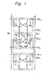
- FIG. 1 schematically illustrates a static RAM cell, in which WL 1 , WL2, ... denote word lines, BL 1 and BL 2 denote bit lines, and MCa, MCb, ... denote memory cells that are connected to intersecting points of the word lines and bit lines.
- Each memory cell consists of load resistors R 1 , R 2 , driving transistors Q 1' Q 2 , and transistors T 1 , T 2 for a transfer gate.
- V cc denotes a high potential level side of the power supply
- V ss denotes a low potential level side.
- the transistors Q 1 and Q 2 constitute a flip-flop circuit, together with the resistors R 1 and R 2 , and one of them is always conductive and the other one is nonconductive.
- the load resistors R 1 and R 2 work to supply power to render the transistors conductive or nonconductive, and to maintain the transistors conductive. From the standpoint of reducing the consumption of power by the memory, however, the load resistors should have a resistance as high as possible.
- memory cells which feature a reduced power requirement. For example, a power-supply current which had so far been required on the order of 50 to 100 mA has now been reduced to 10 to 20 mA when the memory is in the stand-by mode.
- the flow of current is limited when the peripheral circuits are under the stand-by condition in order to reduce the consumption of electric power.
- it is also important to reduce the consumption of electric power by the memory cells.
- the effort to reduce the consumption of power by the peripheral circuits becomes meaningless if a heavy current flows through the memory cells.
- the number of memory cells increases with the increase in the memory capacity, while the peripheral circuits are not so increased. It is, therefore, important to construct memory cells which consume less electric power.
- a polycrystalline silicon film is suited as a high-resistance load resistor for the memory cells.
- This silicon film exhibits a greatly varying resistance depending upon the concentration of impurities; a high resistance can be easily obtained if the concentration of impurities is decreased.
- the concentration of impurities can be easily and accurately adjusted by ion implantation.
- the resistance of a polycrystalline silicon film changes greatly depending upon the temperature. In other words, referring to Figure 2 in which the ordinate represents logarithmic values log R and the abcissa represents the temperature T, the resistance of the polycrystalline silicon film decreases nearly linearly. At an ordinary temperature, for example, the electric current per cell will be from 1 to 100 nA.
- the current increases by about ten times, i.e., the current of. 10 to 1000 nA flows. This presents a serious problem when the memory has large capacities. If it is attempted to increase the load resistance R such that the consumption of electric power remains sufficiently small even at high temperatures, the operation becomes defective at an ordinary temperature. For instance, the operation of the flip-flop circuit becomes slow, and it becomes difficult to sufficiently supply a leakage current across the source and drain of the transistor. Accordingly, the potential at the node changes, and it becomes impossible to render the transistors conductive or nonconductive.
- FIG. 3A An embodiment of the invention is illustrated in Figures 3A and 3B.
- reference numeral 10 denotes a silicon semiconductor substrate
- 12 denotes an insulating film composed of silicon dioxide (Si0 2 ) or the like
- 14 denotes a polycrystalline silicon film that serves as a resistor
- 14a and 14b denote electrodes to which lead wires 20a, 20b will be connected
- 16 denotes a thin insulating film composed of silicon dioxide or the like
- 18 denotes a control electrode mounted on the thin insulating film.
- the control electrode 18 is composed of polycrystalline silicon, but may also be composed of aluminum or the like.
- Figure 3B is a plan view showing the shapes of the electrode 18, the polycrystalline silicon film 14 and the the lead wires 20a, 20b.
- the polycrystalline silicon film 14 is formed through the ordinary steps for forming the transistors. That is, silicon is vaporized onto the insulating film 12 by the CVD method followed by the patterning to obtain a desired shape, and impurities are implanted to a desired concentration, in order to form the polycrystalline silicon film 14. As required, in this case, the concentration of impurities is increased in the portion of the electrodes 14a, 14b.
- the electrode portions serve as a source and a drain, respectively, and the portion therebetween serves as a channel, thereby forming an element such as a MOS transistor with the electrode 18 serving as gate electrode.
- the silicon film 14 is of the n-type, if a negative voltage is applied to the gate electrode 18, a depletion layer is formed in the channel portion and the resistance is increased. If the voltage is increased with the rise in temperature, the reduction of resistance of the silicon film that is caused by the rise in temperature is offset, whereby the resistance vs. temperature coefficient is decreased.
- Figure 4 illustrates a circuit which generates a voltage that will be applied to the control electrode 18.
- Qa through Q j denote MOS transistors that are connected in series between the power supply V cc and the ground; the drain and gate of each of the transistors are short-circuited, so that the transistors work as resistors.
- the transistors Q a through Q i have the same mutual conductance, but the transistor Q. J has a small mutual conductance and works as a leakage resistor.
- Symbols Q m and Q n denote MOS transistors that are connected in series between the positive power supply V cc and the negative power supply V BB , and that form an output stage of the circuit of Figure 4.
- the transistor Q m serves as a resistor with its drain and gate being short-circuited, and the transistor Q n receives the control voltage through the gate thereof, the control voltage being fed from an output terminal F of the transistor of the input stage.
- a connection point G between the transistor Q m and the transistor Q n serves as an output terminal of the circuit, and produces a voltage V 0 that will be applied to the control electrode 18.
- the circuit of Figure 4 receives the same temperature as the semiconductor resistor element shown in Figures 3A and 3B.
- the operation will be described below.
- the voltage V 1 at the point F becomes nearly equal to V cc - i.Vth, where i denotes the number of transistors Q a through Q i , and Vth denotes a threshold voltage of the transistors.
- the transistor Q n Upon receipt of the voltage V 1 , the transistor Q n assumes a given conductivity, and produces at the output terminal G the voltage V o that is obtained by dividing the voltage V cc - (-VBB).
- Figure 5 shows .voltages at the points F and G of Figure 4.
- the threshold voltage Vth of the transistors Q a through Q i decreases with the increase in ambient temperature, whereby the voltage V 1 increases, the conductivity of the transistor Q n increases, and the output voltage V o increases toward the negative side.
- the number of transistors Q a through Q i and the threshold voltage Vth are suitably adjusted, such that the voltage V o will offset the change in resistance of the semiconductor film 14 that is caused by the change in temperature.
- Figure 6 illustrates an example in which the above semiconductor element is incorporated in a memory cell.
- the same reference numerals as those of Figure 1 represent the same members as those of Figure 1, and reference numerals 22, 24 denote gate electrodes of the transistors Q 1 , Q 2 .
- the drain region and the source region (denoted by a, b, V SS ) of the transistors Q 1 , Q 2 extend on both sides of the gate electrodes 22, 24.
- the source and drain regions serve as so-called active regions surrounded by a field region on which is formed a thick insulating film.
- Reference numeral 18 denotes a wiring pattern for the control electrode.
- the wiring pattern is connected to the output terminal V 0 of Figure 5.
- Symbol x denotes the contacting portion.
- the present invention as illustrated in the foregoing, it is possible to obtain a resistor which has a high resistance and a small resistance vs. temperature coeffecient, and which is suited for use as a load resistor for static memory cells.
- the resistor of the present invention can be effectively used for LSI's.
- the semiconductor film may be composed of germanium (Ge) or gallium arsenide (GaAs).
- the circuit of Figure 4 may, of course, be formed in a portion of the chip on which are formed the memory cells, such that the circuit receives the same temperature.
Landscapes
- Engineering & Computer Science (AREA)
- Microelectronics & Electronic Packaging (AREA)
- Computer Hardware Design (AREA)
- Semiconductor Integrated Circuits (AREA)
- Semiconductor Memories (AREA)
- Static Random-Access Memory (AREA)
Applications Claiming Priority (2)
| Application Number | Priority Date | Filing Date | Title |
|---|---|---|---|
| JP55175358A JPS5799765A (en) | 1980-12-12 | 1980-12-12 | Semiconductor resistance element |
| JP175358/80 | 1980-12-12 |
Publications (3)
| Publication Number | Publication Date |
|---|---|
| EP0054471A2 true EP0054471A2 (de) | 1982-06-23 |
| EP0054471A3 EP0054471A3 (en) | 1984-07-18 |
| EP0054471B1 EP0054471B1 (de) | 1989-02-22 |
Family
ID=15994671
Family Applications (1)
| Application Number | Title | Priority Date | Filing Date |
|---|---|---|---|
| EP81401930A Expired EP0054471B1 (de) | 1980-12-12 | 1981-12-04 | Halbleiterwiderstandselement |
Country Status (4)
| Country | Link |
|---|---|
| US (1) | US4504743A (de) |
| EP (1) | EP0054471B1 (de) |
| JP (1) | JPS5799765A (de) |
| DE (1) | DE3176992D1 (de) |
Cited By (1)
| Publication number | Priority date | Publication date | Assignee | Title |
|---|---|---|---|---|
| US6218724B1 (en) * | 1995-10-24 | 2001-04-17 | Mitsubishi Denki Kabushiki Kaisha | Thin film transistor used in semiconductor memory for achieving reduction in power consumption |
Families Citing this family (10)
| Publication number | Priority date | Publication date | Assignee | Title |
|---|---|---|---|---|
| JPS57162181A (en) * | 1981-03-31 | 1982-10-05 | Fujitsu Ltd | Semiconductor memory device |
| JPS5898895A (ja) * | 1981-12-08 | 1983-06-11 | Toshiba Corp | 半導体集積回路 |
| JPS6422107A (en) * | 1987-07-17 | 1989-01-25 | Oki Electric Ind Co Ltd | Voltage level detecting circuit |
| US5208488A (en) * | 1989-03-03 | 1993-05-04 | Kabushiki Kaisha Toshiba | Potential detecting circuit |
| KR910007657B1 (ko) * | 1989-05-23 | 1991-09-30 | 삼성전자 주식회사 | 반도체 온도검출회로 |
| JP3217498B2 (ja) * | 1992-10-29 | 2001-10-09 | 富士通株式会社 | 半導体集積回路装置 |
| CA2093111C (en) * | 1993-03-31 | 1997-03-18 | Thomas W. Macelwee | High value resistive load for an integrated circuit |
| JP3318105B2 (ja) * | 1993-08-17 | 2002-08-26 | 三菱電機株式会社 | 起動回路 |
| JP3625474B1 (ja) * | 2004-04-05 | 2005-03-02 | 富士通テン株式会社 | 接点腐食防止回路 |
| JP4914904B2 (ja) * | 2009-02-03 | 2012-04-11 | 株式会社神鋼環境ソリューション | トロンメル式廃棄物選別装置及び廃棄物処理設備 |
Family Cites Families (10)
| Publication number | Priority date | Publication date | Assignee | Title |
|---|---|---|---|---|
| US3056100A (en) * | 1959-12-04 | 1962-09-25 | Bell Telephone Labor Inc | Temperature compensated field effect resistor |
| US3436689A (en) * | 1964-11-02 | 1969-04-01 | Us Navy | Field effect delay line |
| DE2232274C2 (de) * | 1972-06-30 | 1982-05-06 | Ibm Deutschland Gmbh, 7000 Stuttgart | Statischer Halbleiterspeicher mit Feldeffekttransistoren |
| GB1391959A (en) * | 1972-07-20 | 1975-04-23 | Ferranti Ltd | Semiconductor devices |
| JPS5321992B2 (de) * | 1973-10-17 | 1978-07-06 | ||
| US4164668A (en) * | 1977-05-12 | 1979-08-14 | International Business Machines Corporation | Method of correcting the voltage coefficient of resistors implanted or diffused in a semiconductor substrate |
| US4139785A (en) * | 1977-05-31 | 1979-02-13 | Texas Instruments Incorporated | Static memory cell with inverted field effect transistor |
| US4229753A (en) * | 1977-08-18 | 1980-10-21 | International Business Machines Corporation | Voltage compensation of temperature coefficient of resistance in an integrated circuit resistor |
| US4260911A (en) * | 1979-02-26 | 1981-04-07 | Precision Monolithics, Inc. | Temperature compensated switching circuit and method |
| US4272880A (en) * | 1979-04-20 | 1981-06-16 | Intel Corporation | MOS/SOS Process |
-
1980
- 1980-12-12 JP JP55175358A patent/JPS5799765A/ja active Pending
-
1981
- 1981-11-30 US US06/326,125 patent/US4504743A/en not_active Expired - Fee Related
- 1981-12-04 DE DE8181401930T patent/DE3176992D1/de not_active Expired
- 1981-12-04 EP EP81401930A patent/EP0054471B1/de not_active Expired
Cited By (1)
| Publication number | Priority date | Publication date | Assignee | Title |
|---|---|---|---|---|
| US6218724B1 (en) * | 1995-10-24 | 2001-04-17 | Mitsubishi Denki Kabushiki Kaisha | Thin film transistor used in semiconductor memory for achieving reduction in power consumption |
Also Published As
| Publication number | Publication date |
|---|---|
| EP0054471A3 (en) | 1984-07-18 |
| JPS5799765A (en) | 1982-06-21 |
| US4504743A (en) | 1985-03-12 |
| EP0054471B1 (de) | 1989-02-22 |
| DE3176992D1 (en) | 1989-03-30 |
Similar Documents
| Publication | Publication Date | Title |
|---|---|---|
| US5557231A (en) | Semiconductor device with improved substrate bias voltage generating circuit | |
| US5635731A (en) | SRAM cell with no PN junction between driver and load transistors and method of manufacturing the same | |
| US5135888A (en) | Field effect device with polycrystalline silicon channel | |
| US5187114A (en) | Method of making SRAM cell and structure with polycrystalline P-channel load devices | |
| US4297721A (en) | Extremely low current load device for integrated circuit | |
| US5049970A (en) | High resistive element | |
| US6479905B1 (en) | Full CMOS SRAM cell | |
| US4290185A (en) | Method of making an extremely low current load device for integrated circuit | |
| US6801449B2 (en) | Semiconductor memory device | |
| US4504743A (en) | Semiconductor resistor element | |
| KR940001122B1 (ko) | 반도체장치 및 그 제조방법 | |
| US4780751A (en) | Semiconductor integrated circuit device | |
| US4907059A (en) | Semiconductor bipolar-CMOS inverter | |
| US4384300A (en) | Negative resistance device | |
| US4251876A (en) | Extremely low current load device for integrated circuit | |
| EP0070744B1 (de) | Fieldeffekttransistor mit isoliertem Gate | |
| EP0078222A2 (de) | Bipolare Speicherzelle für integrierte Schaltungen | |
| KR100215851B1 (ko) | 반도체 소자의 구조 | |
| KR960010072B1 (ko) | 반도체 메모리장치 | |
| US4823179A (en) | Semiconductor memory device with flip-flop memory cells which include polycrystalline load resistors | |
| US5027186A (en) | Semiconductor device | |
| EP0111307A2 (de) | Integrierte Halbleiterschaltung mit begrabenem Widerstand | |
| US6218713B1 (en) | Logical circuit, flip-flop circuit and storage circuit with multivalued logic | |
| GB1597725A (en) | Integrated circuit memory | |
| KR0138319B1 (ko) | 스태틱 랜덤 억세스 메모리소자 및 그 제조방법 |
Legal Events
| Date | Code | Title | Description |
|---|---|---|---|
| PUAI | Public reference made under article 153(3) epc to a published international application that has entered the european phase |
Free format text: ORIGINAL CODE: 0009012 |
|
| AK | Designated contracting states |
Designated state(s): DE FR GB NL |
|
| PUAL | Search report despatched |
Free format text: ORIGINAL CODE: 0009013 |
|
| AK | Designated contracting states |
Designated state(s): DE FR GB NL |
|
| 17P | Request for examination filed |
Effective date: 19841207 |
|
| 17Q | First examination report despatched |
Effective date: 19860224 |
|
| GRAA | (expected) grant |
Free format text: ORIGINAL CODE: 0009210 |
|
| PGFP | Annual fee paid to national office [announced via postgrant information from national office to epo] |
Ref country code: FR Payment date: 19890206 Year of fee payment: 9 |
|
| AK | Designated contracting states |
Kind code of ref document: B1 Designated state(s): DE FR GB NL |
|
| PG25 | Lapsed in a contracting state [announced via postgrant information from national office to epo] |
Ref country code: NL Effective date: 19890222 |
|
| REF | Corresponds to: |
Ref document number: 3176992 Country of ref document: DE Date of ref document: 19890330 |
|
| ET | Fr: translation filed | ||
| NLV1 | Nl: lapsed or annulled due to failure to fulfill the requirements of art. 29p and 29m of the patents act | ||
| PG25 | Lapsed in a contracting state [announced via postgrant information from national office to epo] |
Ref country code: GB Effective date: 19891204 |
|
| PLBE | No opposition filed within time limit |
Free format text: ORIGINAL CODE: 0009261 |
|
| STAA | Information on the status of an ep patent application or granted ep patent |
Free format text: STATUS: NO OPPOSITION FILED WITHIN TIME LIMIT |
|
| 26N | No opposition filed | ||
| GBPC | Gb: european patent ceased through non-payment of renewal fee | ||
| PG25 | Lapsed in a contracting state [announced via postgrant information from national office to epo] |
Ref country code: DE Effective date: 19900901 |
|
| PG25 | Lapsed in a contracting state [announced via postgrant information from national office to epo] |
Ref country code: FR Effective date: 19910830 |
|
| REG | Reference to a national code |
Ref country code: FR Ref legal event code: ST |