EP0049127B1 - Bemusterungsverfahren und Verfahren zur Herstellung von elektronischen Vorrichtungen unter Verwendung des genannten Bemusterungsverfahrens - Google Patents
Bemusterungsverfahren und Verfahren zur Herstellung von elektronischen Vorrichtungen unter Verwendung des genannten Bemusterungsverfahrens Download PDFInfo
- Publication number
- EP0049127B1 EP0049127B1 EP81304436A EP81304436A EP0049127B1 EP 0049127 B1 EP0049127 B1 EP 0049127B1 EP 81304436 A EP81304436 A EP 81304436A EP 81304436 A EP81304436 A EP 81304436A EP 0049127 B1 EP0049127 B1 EP 0049127B1
- Authority
- EP
- European Patent Office
- Prior art keywords
- layer
- resin
- process according
- resist
- organosiloxane resin
- Prior art date
- Legal status (The legal status is an assumption and is not a legal conclusion. Google has not performed a legal analysis and makes no representation as to the accuracy of the status listed.)
- Expired
Links
Images


Classifications
-
- H—ELECTRICITY
- H01—ELECTRIC ELEMENTS
- H01L—SEMICONDUCTOR DEVICES NOT COVERED BY CLASS H10
- H01L21/00—Processes or apparatus adapted for the manufacture or treatment of semiconductor or solid state devices or of parts thereof
- H01L21/02—Manufacture or treatment of semiconductor devices or of parts thereof
- H01L21/02104—Forming layers
- H01L21/02107—Forming insulating materials on a substrate
- H01L21/02109—Forming insulating materials on a substrate characterised by the type of layer, e.g. type of material, porous/non-porous, pre-cursors, mixtures or laminates
- H01L21/02112—Forming insulating materials on a substrate characterised by the type of layer, e.g. type of material, porous/non-porous, pre-cursors, mixtures or laminates characterised by the material of the layer
- H01L21/02123—Forming insulating materials on a substrate characterised by the type of layer, e.g. type of material, porous/non-porous, pre-cursors, mixtures or laminates characterised by the material of the layer the material containing silicon
- H01L21/02126—Forming insulating materials on a substrate characterised by the type of layer, e.g. type of material, porous/non-porous, pre-cursors, mixtures or laminates characterised by the material of the layer the material containing silicon the material containing Si, O, and at least one of H, N, C, F, or other non-metal elements, e.g. SiOC, SiOC:H or SiONC
- H01L21/02137—Forming insulating materials on a substrate characterised by the type of layer, e.g. type of material, porous/non-porous, pre-cursors, mixtures or laminates characterised by the material of the layer the material containing silicon the material containing Si, O, and at least one of H, N, C, F, or other non-metal elements, e.g. SiOC, SiOC:H or SiONC the material comprising alkyl silsesquioxane, e.g. MSQ
-
- G—PHYSICS
- G03—PHOTOGRAPHY; CINEMATOGRAPHY; ANALOGOUS TECHNIQUES USING WAVES OTHER THAN OPTICAL WAVES; ELECTROGRAPHY; HOLOGRAPHY
- G03F—PHOTOMECHANICAL PRODUCTION OF TEXTURED OR PATTERNED SURFACES, e.g. FOR PRINTING, FOR PROCESSING OF SEMICONDUCTOR DEVICES; MATERIALS THEREFOR; ORIGINALS THEREFOR; APPARATUS SPECIALLY ADAPTED THEREFOR
- G03F7/00—Photomechanical, e.g. photolithographic, production of textured or patterned surfaces, e.g. printing surfaces; Materials therefor, e.g. comprising photoresists; Apparatus specially adapted therefor
- G03F7/004—Photosensitive materials
- G03F7/075—Silicon-containing compounds
- G03F7/0757—Macromolecular compounds containing Si-O, Si-C or Si-N bonds
-
- H—ELECTRICITY
- H01—ELECTRIC ELEMENTS
- H01L—SEMICONDUCTOR DEVICES NOT COVERED BY CLASS H10
- H01L21/00—Processes or apparatus adapted for the manufacture or treatment of semiconductor or solid state devices or of parts thereof
- H01L21/02—Manufacture or treatment of semiconductor devices or of parts thereof
- H01L21/02104—Forming layers
- H01L21/02107—Forming insulating materials on a substrate
- H01L21/02225—Forming insulating materials on a substrate characterised by the process for the formation of the insulating layer
- H01L21/0226—Forming insulating materials on a substrate characterised by the process for the formation of the insulating layer formation by a deposition process
- H01L21/02282—Forming insulating materials on a substrate characterised by the process for the formation of the insulating layer formation by a deposition process liquid deposition, e.g. spin-coating, sol-gel techniques, spray coating
-
- H—ELECTRICITY
- H01—ELECTRIC ELEMENTS
- H01L—SEMICONDUCTOR DEVICES NOT COVERED BY CLASS H10
- H01L21/00—Processes or apparatus adapted for the manufacture or treatment of semiconductor or solid state devices or of parts thereof
- H01L21/02—Manufacture or treatment of semiconductor devices or of parts thereof
- H01L21/02104—Forming layers
- H01L21/02107—Forming insulating materials on a substrate
- H01L21/02296—Forming insulating materials on a substrate characterised by the treatment performed before or after the formation of the layer
- H01L21/02318—Forming insulating materials on a substrate characterised by the treatment performed before or after the formation of the layer post-treatment
- H01L21/02345—Forming insulating materials on a substrate characterised by the treatment performed before or after the formation of the layer post-treatment treatment by exposure to radiation, e.g. visible light
- H01L21/02348—Forming insulating materials on a substrate characterised by the treatment performed before or after the formation of the layer post-treatment treatment by exposure to radiation, e.g. visible light treatment by exposure to UV light
-
- H—ELECTRICITY
- H01—ELECTRIC ELEMENTS
- H01L—SEMICONDUCTOR DEVICES NOT COVERED BY CLASS H10
- H01L21/00—Processes or apparatus adapted for the manufacture or treatment of semiconductor or solid state devices or of parts thereof
- H01L21/02—Manufacture or treatment of semiconductor devices or of parts thereof
- H01L21/02104—Forming layers
- H01L21/02107—Forming insulating materials on a substrate
- H01L21/02296—Forming insulating materials on a substrate characterised by the treatment performed before or after the formation of the layer
- H01L21/02318—Forming insulating materials on a substrate characterised by the treatment performed before or after the formation of the layer post-treatment
- H01L21/02345—Forming insulating materials on a substrate characterised by the treatment performed before or after the formation of the layer post-treatment treatment by exposure to radiation, e.g. visible light
- H01L21/02351—Forming insulating materials on a substrate characterised by the treatment performed before or after the formation of the layer post-treatment treatment by exposure to radiation, e.g. visible light treatment by exposure to corpuscular radiation, e.g. exposure to electrons, alpha-particles, protons or ions
-
- H—ELECTRICITY
- H01—ELECTRIC ELEMENTS
- H01L—SEMICONDUCTOR DEVICES NOT COVERED BY CLASS H10
- H01L21/00—Processes or apparatus adapted for the manufacture or treatment of semiconductor or solid state devices or of parts thereof
- H01L21/02—Manufacture or treatment of semiconductor devices or of parts thereof
- H01L21/04—Manufacture or treatment of semiconductor devices or of parts thereof the devices having at least one potential-jump barrier or surface barrier, e.g. PN junction, depletion layer or carrier concentration layer
- H01L21/18—Manufacture or treatment of semiconductor devices or of parts thereof the devices having at least one potential-jump barrier or surface barrier, e.g. PN junction, depletion layer or carrier concentration layer the devices having semiconductor bodies comprising elements of Group IV of the Periodic System or AIIIBV compounds with or without impurities, e.g. doping materials
- H01L21/30—Treatment of semiconductor bodies using processes or apparatus not provided for in groups H01L21/20 - H01L21/26
- H01L21/31—Treatment of semiconductor bodies using processes or apparatus not provided for in groups H01L21/20 - H01L21/26 to form insulating layers thereon, e.g. for masking or by using photolithographic techniques; After treatment of these layers; Selection of materials for these layers
- H01L21/312—Organic layers, e.g. photoresist
- H01L21/3121—Layers comprising organo-silicon compounds
- H01L21/3122—Layers comprising organo-silicon compounds layers comprising polysiloxane compounds
Definitions
- This invention relates to a process for producing electronic devices by using a specific energy- sensitive ladder type organo-siloxane resin.
- the ladder type organosiloxane resin used in this invention has such a specific property that when it is irradiated with energy rays such as light rays, X-rays, electron beams and ion beams, it is rendered insoluble in a specific solvent, and a film of the insolubilized resin has high insulating property and heat resistance. Accordingly, after this resin has been used as a material to be etched in the lithographic process, the resin can be used as an insulating layer as it is or after it is heat-treated.
- resin compositions having such a specific property that when they are irradiated with visible rays, ultraviolet rays, X-rays, electron beams, ion beams and the like, polymerization or decomposition occurs to render them insoluble or soluble in specific solvents.
- the lithographic process comprising selectively irradiating a thin layer formed of such resin composition (hereinafter referred to as "resist") with energy rays and selectively dissolving the soluble portion alone in a specific solvent to form a desirable pattern is used for the production of semiconductor devices and the like.
- resists are ordinarily poor in the heat resistance and are not completely chemically stable, and furthermore, they are not sufficiently satisfactory as insulating materials. Therefore, there is ordinarily adopted a method in which a pattern formed of such resist is used as a mask for etching an insulating or conductive material located below the mask of the resist and the resist is removed after completion of the etching operation. In other words, the resist is necessary only as a masking material for the selective etching step and it is not a material to be left as a part of the final product.
- a resist excellent in the heat resistance and insulating property and a resist layer formed by selectively irradiating this resist with energy rays and selectively removing the resist to form a desirable pattern can be used as an insulating layer as it is or after it is subjected to an additional simple treatment.
- Ladder type organosiloxane resins are described in U.S. Patent Specifications 3,162,614; 3,294,738 and 3,944,520, and Specification 3,162,614 specifically teaches that such resins may be used to coat metallic conductors to provide heat resistant insulation processing good electrical properties.
- these three U.S. Patent Specifications do not teach the use of a ladder type organosiloxane resin as a resist resin layer which is capable of being subjected to selective irradiation and development to form a layer having a desired pattern.
- a photo-resist layer as an intermediate insulation layer.
- a process for producing an electronic device in which a layer of a ladder type organo- siloxane resin, represented by the following general formula: where each of the R l 's, which may be the same or different, represents at least one member selected from alkyl groups having 1 to 6 carbon atoms and phenyl and halophenyl groups, each of R 2 and R 3 , which may be the same or different, is selected from alkoxy groups having 1 to 3 carbon atoms and a hydroxyl group each of R 4 and R s , which may be the same or different is selected from hydrogen and alkyl groups having 1 to 3 carbon atoms and n is a number giving a weight average molecular weight of approximately 1000 to 1,000,000 to the ladder type organosiloxane resin, is formed on a lower wiring layer formed on a substrate, and the resin layer is subjected to selective irradiation with energy rays and development treatment to form through holes in the resin layer, characterised in that an
- Lithographic resin compositions are ordinarily sensitive to energy rays such as electromagnetic waves and particle rays or contain sensitizers to these energy rays. This indicates that materials having a resist property are ordinarily poor in the heat resistance.
- the highest applicable temperature of a novolak type resist often used as the photoresist is about 150°C and the glass transition temperature of polymethyl methacrylate (PMMA) as a typical instance of the electron beam resist is 105°C.
- PMMA polymethyl methacrylate
- the ladder type organosiloxane resin of the above general formula [I] used in this invention has a heat resistance of at least 300°C. More specifically, the organosiloxane resin should not undergo heat distortion at a temperature higher than 300°C and should maintain a good adhesion to a substrate to be coated therewith and a top layer to be superposed thereon at such high temperature, and for example, the characteristics of the resin should not be changed at all. even when the resin is allowed to stand in steam maintained at 120°C and 2 atmospheres for scores of hours.
- a polymethylsilsesquioxane (having a weight average molecular weight of 37,000) represented by the following formula [III: is irradiated with electron beams through a mask having a line pattern having a line space of 2 ⁇ m and is then developed with xylene for about 1 minute.
- the resulting resist layer having a line pattern having a line space of 2 pm is exposed to a nitrogen atmosphere maintained at 450°C for 1 hour and then, the pattern precision is examined.
- the electron beam-irrdiated polymethyl- silsequioxane is not influenced by the temperature of 450°C, and it is confirmed that this resin has an excellent heat resistance.
- the side chain R when the side chain R, is a low- molecular-weight alkyl group such as a methyl group, the heating resistance of the resin is especially high, and when R, is a phenyl or halophenyl group, the heat resistance of the resin is relatively low.
- Specific examples of the side chain R are as follows.
- R 2 , R 3 , in the general formula [I] include, for example, hydroxy, methoxy, ethoxy, propoxy, methyl, ethyl and propyl groups
- R 4 and R 5 in the general formula [I] include, for example, hydrogen and methyl, ethyl and propyl groups.
- the ladder type organosiloxane resin of the above formula [I] used in this invention has a weight average molecular weight (Mw) of about 1,000 to about 1,000,000, preferably about 1,500 to about 200,000.
- the weight average molecular weight (Mw) referred to in the instant specification and the appended claims is one determined from the calibration curve prepared according to the gas permeation chromatography by using polystyrene as the reference sample. If the molecular weight is too low, the intended resist pattern can hardly be obtained. In contrast, if the molecular weight is too high,the solubility in a solvent becomes poor and the processability of the resins is reduced.
- the dispersivity i.e., molecular distribution
- the ratio Mw/ Mn of the weight average molecular weight Mw to the number average molecular weight Mn, of the ladder type organosiloxane resin of the above general formula [I] be small and as close to 1 as possible.
- the ratio Mw/Mn is in the range of from about 1.5 to about 4.
- the ladder type organosiloxane resin of the above general formula [I] may be applied in the form of a solution onto a semiconductor device substrate having formed thereon a metal wiring layer.
- Solvents used for the preparation of the coating solution include, for example, aromatic and aliphatic hydrocarbons such as toluene and cyclohexane, cellosolves such as methyl cellosolve acetate, the alcohols and ketones.
- the suitable concentration of the organosiloxane resin in the coating solution varies depending upon the molecular weight of the organosiloxane, the solvent and the intended electronic device, the concentration of the organosiloxane resin is usually in the range of from 4 to 50% by weight.
- the coating may be conducted by spin coating and other conventional coating techniques.
- the adhesion of the polyorganosilsesquioxane to a semiconductor device material is very good, and when the adhesion test was made on silicon (Si), silicon dioxide (Si0 2 ), phosphosilicate glass (PSG) and various electrode metals, it was found that the resin used in this invention has a good adhesion to each of these materials for electronic devices. Furthermore, when the resin was allowed to stand in steam maintained at 120°C and 2 atmospheres for 50 hours, it was found that no degradation of the characteristics took place.
- a resin composition was prepared by mixing 30 parts by volume of a polymethylsilsesquioxane of the above-mentioned structural formula [II] having a number average molecular weight Mn of 24,500, a weight average molecular weight Mw of 96,100 and a dispersivitiy Mw/Mn of 3.9 with 70 parts by volume of a 1:1 volume ratio mixed solvent of isophorone and toluene.
- the resin composition was spin-coated on a silicon (Si) semiconductor substrate (wafer) at a thickness of 1.0 pm and then pre-baked in a nitrogen (N 2 ) atmosphere maintained at 100°C for 1 hour.
- the coated resin was irradiated with electron beams at an acceleration voltage of 10 KeV through a line pattern of a width of 2 pm having a line space of 2 ⁇ m while varying the irradiation time and was then developed with xylene for 30 seconds and with methyl ethyl ketone for 1 minute.
- the irradiated resist film was post-baked in a nitrogen (N 2 ) atmosphere maintained at 120°C for 30 minutes and was then heated in a nitrogen (N 2 ) atmosphere maintained at 450°C for 1 hour. When it was examined by a scanning type electron microscope whether or not deformation of the pattern was caused by heating, no deformation was detected and it was confirmed that the resist film had an excellent heat resistance.
- a resist was prepared by mixing 30 parts by volume of a polymethylsilsesquioxane of the above-mentioned structural formula [II] having a number average molecular weight Mn of 24,500, a weight average molecular weight Mw of 96,100 and a dispersivity M/w/Mn of 3.9 with a 1:1 volume ratio mixed solvent of isophorone and toluene.
- the resist was spin-coated at a thickness of 1.0 um on a silicon wafer and pre-baked in a nitrogen (N 2 ) atmosphere maintained at 100°C for 1 hour.
- the resist was irradiated with proton (H * ) rays at an acceleration voltage of 100 KeV by using a mask having a line pattern of a width of 2 pm having a line space of 2 ⁇ m and was then developed by dipping it in xylene maintained at 20°C for 30 seconds.
- the irradiated resist film was post-baked in a nitrogen atmopshere maintained at 120°C for 30 minutes and then heated in a nitrogen (N 2 ) atmopshere maintained at 450°C for 1 hour.
- N 2 nitrogen
- MIBK methyl isobutyl ketone
- the irradiated resist film was post-baked in a nitrogen (N 2 ) atmosphere maintained at 120°C for 30 minutes and heated in a nitrogen (N 2 ) atmosphere maintained at 450°C for 1 hour.
- N 2 nitrogen
- N 2 nitrogen
- a resist was prepared by mixing 35 parts by volume of a polymethylphenylsilsesquioxane having a number average molecular weight Mn of 1,360, a weight average molecular weight Mw of 4,610 and a dispersivity Mw/Mn of 3.4 which was represented by the above general formula [I] wherein R 1 comprised of methyl (CH 3 ) and phenyl groups at a ratio of 2/1 and R 2 and R 3 stood for an ethoxy group and R 4 and R 5 stood for an ethyl group, with 65 parts by volume of a 1:1 volume ratio mixed solvent of monobutylcellosolve acetate and toluene.
- the resist was spin-coated at a thickness of 1 pm on a silicon (Si) wafer and pre-baked in a nitrogen (N 2 ) atmosphere maintained at 80°C for 30 minutes. Then, the resist was irradiated with electron beams at an acceleration voltage of 30 keV while changing the irradiation time and was then developed by dipping it in toluene maintained at 20°C for 1 minute. The developed resist was promptly dried in a nitrogen (N 2 ) atmosphere. It was confirmed that a resolving power of 1 ⁇ m/1 ⁇ m was obtained at this step. Thus, it was found that the composition of this Example can sufficiently function as a resist (negative type).
- the irradiated resist film was.post-baked in a nitrogen (N 2 ) atmosphere maintained at 120°C for 30 minutes and then heated in a nitrogen (N 2 ) atmosphere maintained at 450°C for 1 hour.
- N 2 nitrogen
- N 2 nitrogen
- a resist was prepared by mixing 35 parts by volume of a polyphenylsilsesquioxane having a number average molecular weight Mn of 1,170, a weight average molecular weight Mw of 2,100 and a dispersivity Mw/Mn of 1.8, which was represented by the above general formula [I] wherein R 1 was a phenyl group and R 2 and R 3 stood for a hydroxyl group and R 4 and R 5 stood for hydrogen, with 65 parts by volume of methyl isobutyl ketone (MIBK).
- MIBK methyl isobutyl ketone
- the so-formed resin composition was spin-coated in a thickness of 1 ⁇ m on a silicon (Si) wafer and the solvent was evaporated at 30°C under a reduced pressure of about 6 ⁇ 10 -3 Torr for 1 hour.
- the thickness of the film after drying was 0.94 ⁇ m.
- the resist film was irradiated with ultraviolet rays emitted from a 500-W xenon-mercury lamp by using a mask having a line pattern of a width of 2 ⁇ m having a line space of 2 pm which were arranged with spaces of 2 pm while changing the irradiation time.
- the irradiated resist film was developed by dipping it in xylene maintained at 20°C for 30 seconds. It was confirmed that a resolving power of 2 pm/2 pm was obtained at this step.
- the irradiated resist film was post-baked in a nitrogen (N 2 ) atmosphere maintained at 120°C for 30 minutes and then heated in a nitrogen (N 2 ) atmosphere maintained at 450°C for 1 hour.
- N 2 nitrogen
- the resist of this Example was excellent in the heat resistance.
- the weight average molecular weight was doubled in this Example, it was found that the necessary ultraviolet ray irradiation time was reduced to about 1/2.
- reference numeral 71 represents a silicon (Si) substrate including active elements such as transistors (not shown) and/or passive elements such as resistors and capacitors (not shown).
- the semiconductor substrate ordinarily comprises a p-type silicon substrate and an n-type silicon epitaxial layer formed on the p-type silicon substrate.
- Such bipolar type semiconductor integrated circuit device is prepared according to a conventional method. More specifically, a donor impurity such as arsenic (As) or antimony (Sb) is selectively doped at a high concentration into the surface of the p-type silicon substrate to form an n'-type doped layer. This selective doping of the donor impurity can be accomplished by a customary selective diffusion or ion implantation method. Then, an n-type silicon epitaxial layer is formed on the p-type silicon substrate including the above-mentioned n'-type doped layer formed thereon.
- a donor impurity such as arsenic (As) or antimony (Sb) is selectively doped at a high concentration into the surface of the p-type silicon substrate to form an n'-type doped layer.
- This selective doping of the donor impurity can be accomplished by a customary selective diffusion or ion implantation method.
- an n-type silicon epitaxial layer is formed on the p-
- This n-type epitaxial layer can be formed, for example, by the gas phase epitaxial growth process in which a phosphorus (p) compound such as phosphine (PH 3 ) and a silicon compound such as monosilane (SiH 4 ) are thermally decomposed.
- a phosphorus (p) compound such as phosphine (PH 3 )
- a silicon compound such as monosilane (SiH 4 ) are thermally decomposed.
- An acceptor impurity such as boron (B) is selectively doped from the surface of the n-type silicon epitaxial layer along a depth reaching the p-type silicon substrate to form a p-type isolation region.
- the epitaxial layer is divided in respective element- forming regions.
- the isolation region may also be formed from an insulating material such as a silicon dioxide film instead of doping of the acceptor impurity.
- an acceptor impurity is selectively doped from the surface of the n-type silicon epitaxial layer to form a p-type base region and/or a p-type resistor region.
- Boron (B) is usually employed as the acceptor impurity, and the acceptor impurity can be doped according to the selective diffusion or ion implantation method.
- the silicon dioxide film on the surface of the n-type epitaxial layer is used as a mask.
- a donor impurity is selectively doped at a high concentration into the p-type base region to form an n +- type emitter region, and simultaneously, this donor impurity is doped also in the surface of the n-type epitaxial layer outside the p-type base region to form an n +- type collector contact region.
- Arsenic (As) or phosphorus (P) is ordinarily used as the donor impurity.
- the doping is accomplished by the selective diffusion or ion implantation method.
- the silicon dioxide film formed on the surface of the n-type epitaxial layer is used as a mask.
- electrode-connecting holes are formed on the silicon dioxide film on the surface of the n-type epitaxial layer.
- Reference numeral 72 represents a silicon dioxide (Si0 2 ) layer having a thickness of about 600 nm formed on the surface of the silicon substrate by the thermal oxidation method or chemical vapor deposition method (CVD method), and reference numerals 73a and 73b represent a lower (first) electrode wiring layer of aluminum (Al) having a thickness of 1.0 ⁇ m, which is selectively disposed on the silicon dioxide (Si0 2 ) layer 72.
- This electrode wiring layer 73 is formed by vacuum deposition of aluminum (AI) and subsequent photo-etching.
- the aluminum electrode wiring layer 73 is connected to the desired regions of elements formed on the semiconductor layer or semiconductor substrate in the above-mentioned electrode-connecting windows (not shown) formed on the above-mentioned silicon dioxide layer 72.
- aluminum for the wiring layer may contain silicon (Si) in an amount of up to several percent.
- the vacuum-deposited aluminum layer is patterned by plasma etching using a positive type photo- resist, for example, OFPR manufactured and supplied by Tokyo Ohka K.K., as a mask and carbon tetrachloride (CCI 4 ) as an etchant gas.
- a positive type photo- resist for example, OFPR manufactured and supplied by Tokyo Ohka K.K., as a mask and carbon tetrachloride (CCI 4 ) as an etchant gas.
- CCI 4 carbon tetrachloride
- An ordinary parallel plate type plasma etching device may be used for this plasma etching treatment.
- a layer 74 of a resin composition comprising a polymethylsilsesquioxane of this invention is formed in a thickness of about 0.8 um to cover the exposed surface of the silicon dioxide (Si0 2 ) layer 72 and the lower wiring layer 73.
- the resin composition layer 74 comprises a polymethylsilsesquioxane resin having, for example, a weight average molecular weight Mw of 59,800, a number average molecular weight Mn of 34,100 and a dispersivity Mw/Mn of 1.75, and this layer 74 is formed by spin-coating the above resin composition at a rotation rate of 3,000 rpm to cover the exposed surface of the silicon dioxide (Si0 2 ) layer 72 and the lower wiring layer 73. Then, the resin composition layer 74 is heat-treated in a nitrogen (N 2 ) atmosphere at about 150°C for about 15 minutes.
- N 2 nitrogen
- the resin composition layer 74 is selectively irradiated with electron beams to effect the exposure treatment.
- the electron beam irradiation is carried out, for example, at an acceleration voltage of 20 KeV in an electron beam dose of 6x10⁻⁶ C/cm 2 .
- the effect of this irradiation is schematically indicated in Fig. 7C by the lines drawn across the layer 74.
- the irradiated resin composition layer 74 is dipped in xylene for 30 seconds and then in methyl ethyl ketone for 60 seconds to effect the development treatment, whereby holes 75 (layer- connecting through holes) are formed in the resin composition resin layer 74. This state is illustrated in Fig. 7C.
- the semiconductor substrate comprising the above-mentioned resin composition layer 74 is heat-treated in a nitrogen (N 2 ) atmosphere at 450°C for about 60 minutes to improve the compactness and heat resistance of the resin composition layer 74.
- an upper (second) wiring layer 76 is formed at a thickness of about 1.5 um to cover the surface of the resin composition layer 74 and the exposed surface of the electrode wiring layer 73a.
- This wiring layer 76 is formed by vacuum deposition of aluminum (Al) and subsequent photo-etching as well as the above-mentioned lower (first) wiring layer 73. This state is . illustrated in Fig. 7D.
- a layer 77 of a resin composition comprising a polymethylsilsesquioxane of this invention is formed at a thickness of about 1.5 um to cover the exposed portion of the above-mentioned first resin composition layer 74 and the upper wiring layer 76.
- the polymethylsilsesquioxane resin constituting this resin composition layer has a weight average molecular weight Mw of 59,800, a number average molecular weight Mn of 34,100 and a dispersivity Mw/Mn of 1.75, as well as the resin used for the resin composition layer 74.
- the resin composition is spin-coated to cover the exposed portion of the resin composition layer 74 and the upper wiring layer 76.
- the resin composition layer 77 is heat-treated in a nitrogen (N 2 ) atmosphere at about 150°C for about 15 minutes.
- the state of forming this resin composition layer 77 is illustrated in Fig. 7E.
- the resin composition layer 77 is selectively irradiated with electron beams to effect the exposure treatment.
- the effect of this irradiation is schematically illustrated in Fig. 7F by the lines drawn across the layer 77.
- the irradiated resin composition layer 77 is then subjected to the development treatment to form holes through which the wiring layer 76 is exposed to provide bonding pads.
- the holes through the layer 77 are not shown in Fig. 7F.
- the conditions adopted for the electron beam irradiation treatment and development treatment of the resin composition layer 77 are the same as those adopted for the above-mentioned resin composition layer 74.
- the semiconductor substrate comprising the so-formed resin composition layer 77 is heat-treated in a nitrogen (N 2 ) atmosphere at 450°C for about 60 minutes to improve the compactness and heat resistance of the resin composition layer 77.
- the resin composition layer 74 is used as the interlaminar insulating layer and the resin composition layer 77 is used as the surface protecting layer or passivating layer.
- Fig. 8 is a sectional partial view illustrating the bipolar type semiconductor integrated circuit device prepared through the steps illustrated in Figs. 7A through 7F.
- reference numerals 81, 82, 83, 84, 85, 86, 87, 88, 89, 90 and 91 represent a p-type silicon substrate, an n +- type buried layer, an n-type silicon expitaxial layer, a p-type isolation region, a p-type base region, an n'-type emitter region, an n +- type collector contact region, a silicon dioxide layer, a collector electrode, a base electrode and an emitter electrode, respectively.
- reference numeral 92 represents an interlaminar insulating layer composed of the resin composition of the present invention
- reference numeral 95 represents a surface protecting insulating layer composed of the resin composition of the present invention
- reference numerals 93 and 94 represent an upper wiring layer.
- each resin composition layer is distinguishable over a conventional insulating layer such as a silicon dioxide (Si0 2 ) film in that photo-resists need not be used independently for the respective layers. Accordingly, the step of patterning the resin composition layers can remarkably be simplified, and this simplification of the preparation process results in a great improvement of the manufacturing yield of the semiconductor device.
- an aluminum (Al) layer 76 is formed on the entire surface and then, a second resin composition layer is formed on the aluminum (Al) layer 76. Then, the second resin layer is subjected to the exposure and development treatment and optionally to the heat treatment, and the aluminum (Al) layer 76 is selectively etched by using the second resin layer as a mask to form an upper wiring layer. Then, a surface protecting layer composed of phosphosilicate glass (PSG) or the resin composition of this invention is formed on the entire surface.
- PSG phosphosilicate glass
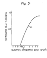
- these resin layers come to have such electric characteristics as a resistivity of about 10 15 Q-cm, a dielectric strength of 1.0 ⁇ 10 6 V/cm, a surface potential of about 10 10 cm- 2 and a dielectric constant of 2.5 to 3.5.
- line I indicates the relation between the treatment time and the percent non-defective in case of the semiconductor device which has as a final protecting layer the resin composition layer of this invention
- organosiloxane resin composition of this invention can be used as interlaminar insulating and surface protecting or passivating insulating layers of a semiconductor device.
- the layer has a thickness of from 0.8 to 2.0 pm.
- the organosiloxane resin composition is used as a surface protecting insulating layer, it is preferable that the layer has a thickness of from 1.0 to 4.0 ⁇ m.
- the organosiloxane resin of this invention after the organosiloxane resin of this invention has functioned as a lithographic resist, it can be used as an insulating layer as it is without removal or after it is subjected to a simple heat treatment at a low temperature, because it is excellent in the heat resistance. Therefore, if the patterning method of this invention using this organosiloxane resin is utilized for the manufacture of semiconductor devices, the manufacturing process can be simplified. Furthermore, since coating of the organosiloxane resin as the resist is accomplished by spin coating, the resulting resist layer is excellent in the evenness, and when an electrode metal or the like is vacuum-deposited on the resist layer, the risk of breaking of the wiring layer is remarkably reduced and the reliability is highly improved.
- Example 6 the fabrication of a bipolar type semiconductor integrated circuit element has been illustrated with reference to Figs. 7A through 7B. It is to be understood, however, that the present invention is not limited thereto but can be applied to the fabrication of discrete semiconductor elements as well as MIS (metal insulator semiconductor) type semiconductor integrated circuit elements.
- MIS metal insulator semiconductor
Claims (10)

auf einer unteren Verdrahtungsschicht gebildet ist, die auf einem Substrat gebildet ist, und die Harzschicht einer selektiven Bestrahlung mit Energiestrahlen und einer Entwicklungsbehandlung ausgesetzt wird, um Durchgangslöcher in der Harzschicht zu bilden, dadurch gekennzeichnet, daß eine obere Verdrahtungsschicht in den genannten Durchgangslöchern so gebildet wird, daß die obere Verdrahtungsschicht mit der genannten unteren Verdrahtungsschicht verbunden ist, und auf der Oberfläche der Organosiloxan-Harzschicht ausgedehnt wird, welche eine isolierende Schicht zwischen oberer und unterer Verdrahtungsschicht bildet.
Applications Claiming Priority (2)
| Application Number | Priority Date | Filing Date | Title |
|---|---|---|---|
| JP134542/80 | 1980-09-27 | ||
| JP55134542A JPS5760330A (en) | 1980-09-27 | 1980-09-27 | Resin composition |
Publications (2)
| Publication Number | Publication Date |
|---|---|
| EP0049127A1 EP0049127A1 (de) | 1982-04-07 |
| EP0049127B1 true EP0049127B1 (de) | 1986-01-15 |
Family
ID=15130746
Family Applications (1)
| Application Number | Title | Priority Date | Filing Date |
|---|---|---|---|
| EP81304436A Expired EP0049127B1 (de) | 1980-09-27 | 1981-09-25 | Bemusterungsverfahren und Verfahren zur Herstellung von elektronischen Vorrichtungen unter Verwendung des genannten Bemusterungsverfahrens |
Country Status (4)
| Country | Link |
|---|---|
| US (1) | US4600685A (de) |
| EP (1) | EP0049127B1 (de) |
| JP (1) | JPS5760330A (de) |
| DE (1) | DE3173512D1 (de) |
Families Citing this family (55)
| Publication number | Priority date | Publication date | Assignee | Title |
|---|---|---|---|---|
| CA1204527A (en) * | 1982-08-13 | 1986-05-13 | Theodore F. Retajczyk, Jr. | Polymeric films for electronic circuits |
| US4510173A (en) * | 1983-04-25 | 1985-04-09 | Kabushiki Kaisha Toshiba | Method for forming flattened film |
| EP0130599B1 (de) * | 1983-06-29 | 1988-08-10 | Fuji Photo Film Co., Ltd. | Photolösungsfähige Zusammensetzung |
| JPS60117242A (ja) * | 1983-11-29 | 1985-06-24 | Fujitsu Ltd | 微細パタ−ン形成材料 |
| EP0163538B1 (de) * | 1984-05-30 | 1989-11-23 | Fujitsu Limited | Bilderzeugendes Material, Herstellung und Anwendung desselben |
| JPS60254036A (ja) * | 1984-05-30 | 1985-12-14 | Fujitsu Ltd | パタ−ン形成方法 |
| JPS60254132A (ja) * | 1984-05-31 | 1985-12-14 | Fujitsu Ltd | パタ−ン形成材料 |
| JPS6129153A (ja) * | 1984-07-20 | 1986-02-10 | Fujitsu Ltd | 凹凸基板の平坦化方法 |
| US4670299A (en) * | 1984-11-01 | 1987-06-02 | Fujitsu Limited | Preparation of lower alkyl polysilsesquioxane and formation of insulating layer of silylated polymer on electronic circuit board |
| JPS61144639A (ja) * | 1984-12-19 | 1986-07-02 | Hitachi Ltd | 放射線感応性組成物及びそれを用いたパタ−ン形成法 |
| JPS61201430A (ja) * | 1985-03-04 | 1986-09-06 | Fujitsu Ltd | 半導体装置用シリコ−ン樹脂膜及びその形成方法 |
| EP0215069B1 (de) * | 1985-03-07 | 1991-04-10 | Hughes Aircraft Company | Polysiloxanschutzlack für ionen- und elektronenstrahl-lithographie |
| EP0204963B1 (de) * | 1985-05-10 | 1993-01-13 | Hitachi, Ltd. | Verwendung von in alkalische Milieu löslichen Silsesquioxanpolymeren in einem Resist zur Herstellung von electronischen Teilen |
| US4663414A (en) * | 1985-05-14 | 1987-05-05 | Stauffer Chemical Company | Phospho-boro-silanol interlayer dielectric films and preparation |
| JP2607870B2 (ja) * | 1985-07-26 | 1997-05-07 | 富士写真フイルム株式会社 | 画像形成方法 |
| DE3760030D1 (en) * | 1986-02-07 | 1989-02-02 | Nippon Telegraph & Telephone | Photosensitive and high energy beam sensitive resin composition containing substituted polysiloxane |
| US4782009A (en) * | 1987-04-03 | 1988-11-01 | General Electric Company | Method of coating and imaging photopatternable silicone polyamic acid |
| US4855199A (en) * | 1987-04-03 | 1989-08-08 | General Electric Company | Photopatterned product of silicone polyamic acid on a transparent substrate |
| US4801507A (en) * | 1987-07-02 | 1989-01-31 | Akzo American Inc. | Arylsiloxane/silicate compositions useful as interlayer dielectric films |
| US4758620A (en) * | 1987-07-02 | 1988-07-19 | Akzo America Inc. | Blend of solvent and arylsiloxane interlayer dielectric materials |
| US4765866A (en) * | 1987-07-02 | 1988-08-23 | Akzo America Inc. | Energy ray curing of arylsiloxane/silicate compositions and subsequent etching thereof |
| US5057396A (en) * | 1988-09-22 | 1991-10-15 | Tosoh Corporation | Photosensitive material having a silicon-containing polymer |
| US5089303A (en) * | 1989-04-24 | 1992-02-18 | Akzo America Inc. | Blend of solvent and photocurable arylsiloxane materials |
| US5106658A (en) * | 1989-04-24 | 1992-04-21 | Akzo Nv | Hardness improvement of film containing arylsiloxane and organosilicate |
| US5118742A (en) * | 1989-04-24 | 1992-06-02 | Akzo Nv | Blend of silicate and photocurable arylsiloxane materials |
| US5059512A (en) * | 1989-10-10 | 1991-10-22 | International Business Machines Corporation | Ultraviolet light sensitive photoinitiator compositions, use thereof and radiation sensitive compositions |
| US5110711A (en) * | 1989-10-10 | 1992-05-05 | International Business Machines Corporation | Method for forming a pattern |
| US5098816A (en) * | 1989-10-10 | 1992-03-24 | International Business Machines Corporation | Method for forming a pattern of a photoresist |
| US5024969A (en) * | 1990-02-23 | 1991-06-18 | Reche John J | Hybrid circuit structure fabrication methods using high energy electron beam curing |
| EP0464614B1 (de) * | 1990-06-25 | 1999-09-29 | Matsushita Electronics Corporation | Licht- oder strahlungsempfindliche Zusammensetzung |
| JPH04233732A (ja) * | 1990-08-16 | 1992-08-21 | Motorola Inc | 半導体の製造工程で使用するスピン・オン誘電体 |
| US5093225A (en) * | 1990-09-14 | 1992-03-03 | Gte Laboratories Incorporated | Processing method for fabricating electrical contacts to mesa structures in semiconductor devices |
| US5312684A (en) * | 1991-05-02 | 1994-05-17 | Dow Corning Corporation | Threshold switching device |
| JPH05197304A (ja) * | 1992-01-20 | 1993-08-06 | Hitachi Ltd | 溶着部材 |
| JP2934353B2 (ja) * | 1992-06-24 | 1999-08-16 | 三菱電機株式会社 | 半導体装置およびその製造方法 |
| US5397741A (en) * | 1993-03-29 | 1995-03-14 | International Business Machines Corporation | Process for metallized vias in polyimide |
| TW434458B (en) * | 1995-04-04 | 2001-05-16 | Shinetsu Chemical Co | Chemically amplified positive resist compositions |
| MY113904A (en) * | 1995-05-08 | 2002-06-29 | Electron Vision Corp | Method for curing spin-on-glass film utilizing electron beam radiation |
| US6607991B1 (en) | 1995-05-08 | 2003-08-19 | Electron Vision Corporation | Method for curing spin-on dielectric films utilizing electron beam radiation |
| JP2697680B2 (ja) * | 1995-05-31 | 1998-01-14 | 日本電気株式会社 | 珪素含有高分子化合物および感光性樹脂組成物 |
| US6157079A (en) * | 1997-11-10 | 2000-12-05 | Citizen Watch Co., Ltd | Semiconductor device with a bump including a bump electrode film covering a projecting photoresist |
| JP3543669B2 (ja) * | 1999-03-31 | 2004-07-14 | 信越化学工業株式会社 | 絶縁膜形成用塗布液及び絶縁膜の形成方法 |
| KR100804873B1 (ko) * | 1999-06-10 | 2008-02-20 | 얼라이드시그날 인코퍼레이티드 | 포토리소그래피용 sog 반사방지 코팅 |
| KR20000063142A (ko) * | 2000-02-17 | 2000-11-06 | 이응찬 | 폴리오르가노실세스키옥산 제조용 출발물질,폴리오르가노실세스키옥산 및 폴리오르가노실세스키옥산제조방법 |
| US6368400B1 (en) * | 2000-07-17 | 2002-04-09 | Honeywell International | Absorbing compounds for spin-on-glass anti-reflective coatings for photolithography |
| US6653045B2 (en) * | 2001-02-16 | 2003-11-25 | International Business Machines Corporation | Radiation sensitive silicon-containing negative resists and use thereof |
| AU2003216067A1 (en) * | 2002-01-17 | 2003-09-02 | Silecs Oy | Poly(organosiloxane) materials and methods for hybrid organic-inorganic dielectrics for integrated circuit applications |
| US8053159B2 (en) | 2003-11-18 | 2011-11-08 | Honeywell International Inc. | Antireflective coatings for via fill and photolithography applications and methods of preparation thereof |
| US7659050B2 (en) * | 2005-06-07 | 2010-02-09 | International Business Machines Corporation | High resolution silicon-containing resist |
| US20070212886A1 (en) * | 2006-03-13 | 2007-09-13 | Dong Seon Uh | Organosilane polymers, hardmask compositions including the same and methods of producing semiconductor devices using organosilane hardmask compositions |
| US8642246B2 (en) | 2007-02-26 | 2014-02-04 | Honeywell International Inc. | Compositions, coatings and films for tri-layer patterning applications and methods of preparation thereof |
| US8557877B2 (en) | 2009-06-10 | 2013-10-15 | Honeywell International Inc. | Anti-reflective coatings for optically transparent substrates |
| KR101249798B1 (ko) * | 2010-08-18 | 2013-04-03 | 한국과학기술연구원 | 선택적으로 구조가 제어된 폴리실세스퀴옥산의 제조방법 및 이로부터 제조된 폴리실세스퀴옥산 |
| US8864898B2 (en) | 2011-05-31 | 2014-10-21 | Honeywell International Inc. | Coating formulations for optical elements |
| WO2016167892A1 (en) | 2015-04-13 | 2016-10-20 | Honeywell International Inc. | Polysiloxane formulations and coatings for optoelectronic applications |
Citations (3)
| Publication number | Priority date | Publication date | Assignee | Title |
|---|---|---|---|---|
| US3162614A (en) * | 1962-02-23 | 1964-12-22 | Gen Electric | Process for making benzene-soluble phenyl silsesquioxane |
| US3294738A (en) * | 1963-12-23 | 1966-12-27 | Gen Electric | Method for making arylsilsesquioxane ladder polymers |
| US4209356A (en) * | 1978-10-18 | 1980-06-24 | General Electric Company | Selective etching of polymeric materials embodying silicones via reactor plasmas |
Family Cites Families (6)
| Publication number | Priority date | Publication date | Assignee | Title |
|---|---|---|---|---|
| US162017A (en) * | 1875-04-13 | Improvement in door-bolts | ||
| NL290390A (de) * | 1962-03-29 | |||
| US4041190A (en) * | 1971-06-29 | 1977-08-09 | Thomson-Csf | Method for producing a silica mask on a semiconductor substrate |
| US3944520A (en) * | 1974-04-18 | 1976-03-16 | Andrianov Kuzma A | Cyclolinear polyorganosiloxanes and method for preparing same |
| US4209358A (en) * | 1978-12-04 | 1980-06-24 | Western Electric Company, Incorporated | Method of fabricating a microelectronic device utilizing unfilled epoxy adhesive |
| US4349609A (en) * | 1979-06-21 | 1982-09-14 | Fujitsu Limited | Electronic device having multilayer wiring structure |
-
1980
- 1980-09-27 JP JP55134542A patent/JPS5760330A/ja active Granted
-
1981
- 1981-09-25 DE DE8181304436T patent/DE3173512D1/de not_active Expired
- 1981-09-25 EP EP81304436A patent/EP0049127B1/de not_active Expired
-
1985
- 1985-05-29 US US06/738,891 patent/US4600685A/en not_active Expired - Lifetime
Patent Citations (3)
| Publication number | Priority date | Publication date | Assignee | Title |
|---|---|---|---|---|
| US3162614A (en) * | 1962-02-23 | 1964-12-22 | Gen Electric | Process for making benzene-soluble phenyl silsesquioxane |
| US3294738A (en) * | 1963-12-23 | 1966-12-27 | Gen Electric | Method for making arylsilsesquioxane ladder polymers |
| US4209356A (en) * | 1978-10-18 | 1980-06-24 | General Electric Company | Selective etching of polymeric materials embodying silicones via reactor plasmas |
Also Published As
| Publication number | Publication date |
|---|---|
| JPS5760330A (en) | 1982-04-12 |
| EP0049127A1 (de) | 1982-04-07 |
| DE3173512D1 (en) | 1986-02-27 |
| JPS6360374B2 (de) | 1988-11-24 |
| US4600685A (en) | 1986-07-15 |
Similar Documents
| Publication | Publication Date | Title |
|---|---|---|
| EP0049127B1 (de) | Bemusterungsverfahren und Verfahren zur Herstellung von elektronischen Vorrichtungen unter Verwendung des genannten Bemusterungsverfahrens | |
| US4657843A (en) | Use of polysilsesquioxane without hydroxyl group for forming mask | |
| EP0167854B1 (de) | Zusammensetzung für die Zwischenschicht eines aus drei Schichten bestehenden Photoresistsystems und Verfahren zur Herstellung eines Resistbildes | |
| US6589862B2 (en) | Process of using siloxane dielectric films in the integration of organic dielectric films in electronic devices | |
| JP4133968B2 (ja) | 反射防止ハードマスク組成物とそれを用いた半導体デバイスの製造方法 | |
| EP0970519B1 (de) | Integration von niedrig-k polymeren in dielektrischen zwischenschichten unter verwendung von kontrollierten elektronenstrahlen | |
| US6831005B1 (en) | Electron beam process during damascene processing | |
| EP0130338B1 (de) | Schutzschichtstruktur, Verfahren zur Herstellung und Bilderzeugung | |
| EP0432905B1 (de) | Polysilphenylensiloxan, Verfahren zu deren Herstellung, Resistmasse und Halbleitervorrichtungen | |
| US6489030B1 (en) | Low dielectric constant films used as copper diffusion barrier | |
| KR100453312B1 (ko) | 불소함유실리콘네트워크폴리머,그의절연막및그를이용한전자장치 | |
| EP0067067B1 (de) | Trocken entwickelbare negativ arbeitende Resistzusammensetzung | |
| US6693355B1 (en) | Method of manufacturing a semiconductor device with an air gap formed using a photosensitive material | |
| JP3132885B2 (ja) | レジスト組成物及びそれを用いるパターン形成方法 | |
| JPH06291273A (ja) | 半導体集積回路の製造方法 | |
| JP3633987B2 (ja) | 放射線感応性樹脂組成物及び酸化シリコン膜形成方法 | |
| WO1986000425A1 (en) | Adhesion promoter and process for plasma oxide surfaces | |
| JPS6256956A (ja) | 耐熱性絶縁パタ−ンの製造方法 | |
| JP3249718B2 (ja) | フッ素含有シリコンネットワークポリマとその絶縁膜およびその製法 | |
| EP0680081A2 (de) | Verfahren zur Bildung dünner Schichten und elektronischer Vorrichtung mit dünnen Schichten | |
| JPH04184444A (ja) | 感光性耐熱樹脂組成物と半導体装置の製造方法 | |
| JPS60140734A (ja) | 多層配線構造体およびその製造方法 | |
| JPH06267937A (ja) | ケイ酸ガラス薄膜の形成方法 |
Legal Events
| Date | Code | Title | Description |
|---|---|---|---|
| PUAI | Public reference made under article 153(3) epc to a published international application that has entered the european phase |
Free format text: ORIGINAL CODE: 0009012 |
|
| AK | Designated contracting states |
Designated state(s): DE FR GB NL |
|
| 17P | Request for examination filed |
Effective date: 19820614 |
|
| GRAA | (expected) grant |
Free format text: ORIGINAL CODE: 0009210 |
|
| AK | Designated contracting states |
Designated state(s): DE FR GB NL |
|
| ET | Fr: translation filed | ||
| REF | Corresponds to: |
Ref document number: 3173512 Country of ref document: DE Date of ref document: 19860227 |
|
| PLBE | No opposition filed within time limit |
Free format text: ORIGINAL CODE: 0009261 |
|
| STAA | Information on the status of an ep patent application or granted ep patent |
Free format text: STATUS: NO OPPOSITION FILED WITHIN TIME LIMIT |
|
| 26N | No opposition filed | ||
| PGFP | Annual fee paid to national office [announced via postgrant information from national office to epo] |
Ref country code: FR Payment date: 19990909 Year of fee payment: 19 |
|
| PGFP | Annual fee paid to national office [announced via postgrant information from national office to epo] |
Ref country code: GB Payment date: 19990922 Year of fee payment: 19 |
|
| PGFP | Annual fee paid to national office [announced via postgrant information from national office to epo] |
Ref country code: DE Payment date: 19990927 Year of fee payment: 19 |
|
| PGFP | Annual fee paid to national office [announced via postgrant information from national office to epo] |
Ref country code: NL Payment date: 19990930 Year of fee payment: 19 |
|
| PG25 | Lapsed in a contracting state [announced via postgrant information from national office to epo] |
Ref country code: GB Free format text: LAPSE BECAUSE OF NON-PAYMENT OF DUE FEES Effective date: 20000925 |
|
| PG25 | Lapsed in a contracting state [announced via postgrant information from national office to epo] |
Ref country code: NL Free format text: LAPSE BECAUSE OF NON-PAYMENT OF DUE FEES Effective date: 20010401 |
|
| GBPC | Gb: european patent ceased through non-payment of renewal fee |
Effective date: 20000925 |
|
| PG25 | Lapsed in a contracting state [announced via postgrant information from national office to epo] |
Ref country code: FR Free format text: LAPSE BECAUSE OF NON-PAYMENT OF DUE FEES Effective date: 20010531 |
|
| NLV4 | Nl: lapsed or anulled due to non-payment of the annual fee |
Effective date: 20010401 |
|
| PG25 | Lapsed in a contracting state [announced via postgrant information from national office to epo] |
Ref country code: DE Free format text: LAPSE BECAUSE OF NON-PAYMENT OF DUE FEES Effective date: 20010601 |
|
| REG | Reference to a national code |
Ref country code: FR Ref legal event code: ST |