EP0032015A2 - Kundenprogrammierbare Vorrichtung mit Testbits - Google Patents
Kundenprogrammierbare Vorrichtung mit Testbits Download PDFInfo
- Publication number
- EP0032015A2 EP0032015A2 EP80304531A EP80304531A EP0032015A2 EP 0032015 A2 EP0032015 A2 EP 0032015A2 EP 80304531 A EP80304531 A EP 80304531A EP 80304531 A EP80304531 A EP 80304531A EP 0032015 A2 EP0032015 A2 EP 0032015A2
- Authority
- EP
- European Patent Office
- Prior art keywords
- test
- rows
- row
- bit
- word
- Prior art date
- Legal status (The legal status is an assumption and is not a legal conclusion. Google has not performed a legal analysis and makes no representation as to the accuracy of the status listed.)
- Granted
Links
Images


Classifications
-
- G—PHYSICS
- G11—INFORMATION STORAGE
- G11C—STATIC STORES
- G11C29/00—Checking stores for correct operation ; Subsequent repair; Testing stores during standby or offline operation
- G11C29/02—Detection or location of defective auxiliary circuits, e.g. defective refresh counters
-
- G—PHYSICS
- G11—INFORMATION STORAGE
- G11C—STATIC STORES
- G11C29/00—Checking stores for correct operation ; Subsequent repair; Testing stores during standby or offline operation
- G11C29/04—Detection or location of defective memory elements, e.g. cell constructio details, timing of test signals
- G11C29/08—Functional testing, e.g. testing during refresh, power-on self testing [POST] or distributed testing
- G11C29/12—Built-in arrangements for testing, e.g. built-in self testing [BIST] or interconnection details
- G11C29/18—Address generation devices; Devices for accessing memories, e.g. details of addressing circuits
- G11C29/24—Accessing extra cells, e.g. dummy cells or redundant cells
-
- G—PHYSICS
- G11—INFORMATION STORAGE
- G11C—STATIC STORES
- G11C29/00—Checking stores for correct operation ; Subsequent repair; Testing stores during standby or offline operation
- G11C29/52—Protection of memory contents; Detection of errors in memory contents
Definitions
- the present invention relates generally to field programmable devices, and more particularly to field programmable devices such as ROM's (Read Only Memories), PROM's (Programmable Read Only Memories), FPLA's (Field Programmable Logic Arrays) and the like, capable of being subjected to functional tests before information is written therein.
- ROM's Read Only Memories
- PROM's Programmable Read Only Memories
- FPLA's Field Programmable Logic Arrays
- field programmable devices such as PROM's and ROM's, that is, memory devices capable of having information written therein on the spot, all memory cells within the memory device, before write-in of information, are in a "0" (low) or "1" (high) state, and hence tests cannot be performed to detect whether a memory cell selected is in a normal or abnormal state.
- One example of a conventional memory device of the above type comprises X and Y address inverters , an X-decoder driver, a Y-decoder, a memory cell part, a multiplexer, and an output circuit.
- X and Y address inverters X and Y address inverters
- an X-decoder driver a Y-decoder
- a memory cell part a multiplexer
- an output circuit for example
- Variationsof word line capacity cause change in rise-up characteristics of a word line and in read-out time. Such changes'are generally of small amounts, but since field programmable devices, especially high-speed Schottky-type PROM's and the like, have a fast average access time of 20 nsec in the 4-kilobit class, even the slightest change can become a problem.
- Word line capacity is affected by manufacturing processes, and thus, computation of word line capacity by calculation is difficult, and preferably actual measurements should be made.
- the write-in ratio of the test bit row and test word are both 50% , and hence the device is capable of being subjected to a speed check relating to a 50% write-in ratio, but incapable of being subjected to speed checks in remaining parts or for other write-in ratios. Therefore, when a user performs a 100% write-in (this is done quite often), access time can be much higher than the nominal value indicated by a 50 % write-in check.
- a field programmable device comprising a memory cell part having a plurality of test bit rows provided along bit lines of the memory cell part and/or a plurality of test word rows provided along word lines of the memory cell part, characterised in that at least one of the test bit and/or test word rows is written-in with a different write-in ratio from that of the other test bit and/or test word row or rows.
- An embodiment of the present invention can provide a field programmable device in which the above described problems have been overcome.
- An embodiment of the present invention provides a field programmable device in which a plurality of test bit rows are provided along bit lines and/or a plurality of test word rows are provided along word lines in a memory cell part of the device, in which at least one of the above rows hasLwrite-in ratio different from that of the other rows.
- An embodiment of the present invention can provide for the performance of complete tests.on DC and AC characteristics of the field programmable device before the shipment of the device.
- Transistors TR 1 are transistors in output stages of decoder driver 11, which are connected to corresponding word lines l 1 , l 2 , whereas Transistors TR 2 represent memory cells not yet having information written therein.
- Diodes D 1 represent diodes formed when transistor emitter and base junctions are short circuited, to show memory cells having written-in information "1" (high).
- FIGS. 3A to 3C are, respectively, an equivalent circuit diagram of the memory cell part not yet having written information therein, and respective cross-sectional diagrams of the memory cell part respectively taken along broken lines I and II of FIG. 3A.
- an n-type semiconductor layer 20 which is to provide the functions of a collector, is epitaxially grown on a p -type silicon semiconductor base 19.
- a plurality of p +- type regions 21 which are to be the bases, are formed on top of the n-type semiconductor layer 20, and n type regions 22 are formed on top of the p + type regions 21.
- the word lines l 1 and f 2 are formed by the n +- type regions 23 embedded below the n-type layer 20, while the bit lines b 1 to b 3 are provided by metal wirings 24 formed on the surface.
- Layers 25 are insulative membranes, + and p -type isolation regions 26 separate the different word lines.
- FIG.4 is a diagram illustrative of the memory cell part of FIG. 2.
- all the memory cells of the memory cell part 14 are in a state in which information is not written in the cells , but information is written selectively in test bits and the test words.
- the cells in which information is written are shown by the cross-hatched squares, and the remaining (un-written) cells are shown un- by / marked squares..
- the reason for the necessity to selectively write in the information "0" and "1" will now be described.
- the selection of the memory cells is performed by the Y-address inverter 12, Y-decoder 13, and multiplexer 15 in relation to the bit line side, and performed by the X-address inverter 10 , and X-decoder driver 11 in relation to the word line side.
- the latter concerning the word line side, will be described along with FIGS. 5 and 6-which outline circuits for the word line side.
- the address inverter 10 comprises a plurality of rows each having two inverters connected in series, namely , I1 and I 2 , I 3 and I4, and so on.
- the decoder driver 11 comprises a plurality of rows each having a NAND-gate, namely , NG 1 , NG 2 , and so on. Respective address signal bits A 0 , A 1 , A 2 Vietnamese of an address signal are applied to respective input terminals of the rows having two series connected inverters. Accordingly, inverted and non-inverted signals, namely, A 0 , A 0 , A 1 , A 1 ,..., can be obtained.
- a decoder driver 11 corresponding to the two-bit address signal bits A 0 and A 1 is shown in Figure 5 for this example in which the selection from four word lines is performed by using two bits; however, if an address signal has five address signal bits, namely A 0 through A4, word line selection from 2 5 , or thirty-two word lines is possible, and in this case, ten inverters, I 1 to I 10 , and thirty-two NAND-gates are required.
- FIG.6 further illustrates/selection system on the word line side and including a portion of the memory cell part 14.
- memory cells M 11 , M 12' ....M 21 , M 22 , ... are respectively provided at each of the intersection points between the word lines l 1 ,l 2 , ... and bit lines b1, b 2 ,...
- the address signal bit A0of the address signal is shown.
- the memory cells of a PROM are constructed of fuses or p-n junctions ; in this example the latter is indicated, and the write-in of information is effected by destroying the junction between the base and emitter of an npn-transistor.
- the write-in of information is performed by the user, and the write-in of information is not performed before shipment of the devices by the manufacturer .
- the above current which flows toward the NAND-gate through the bit line and word line upon generation of a low-level output by the NAND-gate, as described above, does not flow upon addressing. Accordingly, it is impossible (for the manufacturer, before write in) to detect whether a desired word line has actually been selected or not, or whether a problem such as a break in the wiring exists or not.
- the selection of a word line can be successfully performed only when the address inverters, decoder driver, and their wiring are normal, and therefore, even though assumptions can be made in relation to non-selection of a word line due to abnormalities, it is impossible to detect the whereabouts of the cause.
- Test bits can be provided in the memory cell part to overcome the above problem. If it is assumed that the memory cells M 11 , M 12' .... of FIG. 6 are for test bits inserted in an additional (test) bit line of the memory cell part, and that a code"1,0,1,0, " are written in these test bits, a current flows and the line l 1 is selected when the address signal bit A 0 is "0", and, no current flows and the line l 2 is selected when the address signal bit A O is "1" . Accordingly, it can be assumed that the inverter I 1 , NAND-gate NG 1 and their wiring are normal when current flows and does not flow as expected.
- the resultant overall output state is the same when the inverter I I is in a fixed "1" state and the inverter I 2 is in a normal state, as when the inverter I 1 is in a fixed "1” state and the inverter I 2 is in a fixed "0” state.
- the result is the same when the inverter I1 is in a fixed "0” state and the inverter 1 2 is in a normal state, as when the inverter I 1 is in a fixed "0” state and the inverter 1 2 is in a fixed "1” state.
- Table 1 there are seven possible output state combinations, as shown in Table 1.
- cases (1) to (7) in Table 1 the only normal state obtained is in case (1), and all the other cases (2) through (7) are abnormal states (cases (2) and (3) are partially normal and partially abnormal, and thus abnormal considered as a whole).
- the object is to detect the above abnormal cases by use of the test bits, but differences occur according to the contents stored in the test bits, as shown in Table 2.
- FIG. 7 shows that test bits b 11 and b 21 , corresponding to the above memory cells M 11 and M 21 , are respectively "0" and “1” as described above, and that succeeding test bits b 31 and b 41 should contain the inverse code of that formed by the test bits b11 and b 21 , namely "1" and "0", respectively.
- the next succeeding test bits b 51' b 61' b 71 and b 81 should contain the inverse code of that formed by the test bits b 11 , b 21' b 31' and b 41 , namely, "1,0,0,1".
- the rest of the code can be obtained as shown in FIG. 7, and the same code pattern should be inserted into the test word TW 1 to perform the above described valid judgements (see FIG.2).
- the address inverters as well as the decoder driver can be checked for normal or abnormal states.
- only thecurrent absorbing capacity of half the decoder drivers can be checked, since the other half of the decoders are connected to bits containing the information "0" (This is because the code pattern contains the same number of "O"s and "l"s).
- the write-in/information is performed by selecting a word line, and applying a large voltage on the bit line to pass a large current of about 200 mA through the bit line, memory cell, word line, and NAND-gate.
- this large current cannot be passed through the NAND-gates connected to the test bits in an OFF state, and the current absorbing capacity of the NAND-gates cannot be checked.
- the object of the above stated invention in the United States Patent Application No.95782 was to compensate for the above described problems.
- an additional bit line and an additional word line were provided and a test bit row TB 2 and test word row TW 2 were connected to these additional lines.
- the information written-in into these test bit cells were made to be the inverse of those written-in into the first test bit line and first test word line, namely, "1,0,0,1,0, etc.
- the contents written-in into the test bit pairs mentioned are the same, but the actual physical geographical test bit arrangement in the memory cell part is changed so that the stored contents of those test bits are the inverse of those of their neighbouring test bits (in the same test bit line), namely, "0,1,0,1,0, 1 ." or "1,0,1,0,1 ... " . .
- FIGS. 8A and 8B illustrate the above described test bit arrangement for a two-bit address signal and four word lines.
- FIG. 8A shows the case where the code "0,1,1,0” is stored in the test bits (i.e. in actual physical consecutive test bits in a test bit line)
- FIG. 8B shows a case where the code "0,1,0,1" is stored in the test bits (i.e. in actual physically consecutive test bits in a test bit line).
- test bits b 11 , b 21' b 31' and b 41 selected by the two -bit address signals "00" , "01", “10", and “11” are written-in with the information "0,1,1,0", respectively,- but the actual physical geographical arrangement of bits in the memory cell part in the case shown by FIG. 8B is "0,1,0,1" .
- the circuit of FIG. 8B processes address signal bits differently. Accordingly, by the arrangement shown in FIG. 8B, a different result is . obtained when a short-circuit exists between neighbouring wires of a word line, as opposed to that of a normal state, and the abnormality can be detected immediately.
- FIGS. 9A and 9B respectively show test bit arrangements for six-bit address signal and sixty-four memory cells.
- FIG. 9A shows a test bit arrangement including a countermeasure against short-circuits in the wiring, while the arrangement of FIG. 9B does not.
- the cross-hatched squares (bits) indicate bits containing the information "1"
- the unmarked squares (bits) indicate bits containing the information "0" .
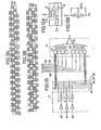
- FIG. 10 A detection circuit for detecting the defect in the multiplexer is shown in FIG. 10.
- the memory cell part 14 of FIG. 1 is divided into a plurality of memory cell groups, and a system is used in which each of the memory cell groups are selectively connected to the output circuit 16 by use of a multiplexer 15 connected between the output circuit 16 and the memory cell groups.
- this multiplexer 15 also needs to be tested as to whether it is normally operational or not.
- a test word can be provided which generates an output representing the output of each of the memory cell groups, and an output can be obtained by switching over these outputs by a switching signal.
- G 1 to G 8 are AND-gates
- G 9 is an OR-gate constructing the multiplexer 15.
- Output circuits of each of the memory cell groups are designated by g 1 through g 82 and selection signals bits for selecting the AND-gates G1 to G 8 are designated by A6 through A 8 .
- there are eight memory cell groups that is, there are eight AND-gates, and hence the output of one of the AND-gates is selected to be high ("1") by the selection signal formed by the three selection signal bits A 6 through A 8 .
- Abnormalities can be checked by setting a test word to contain "0,1,1,0,1,0,0,1" and considering a possibility of breaks in the wiring, it is desirable to set the physical arrangement of the test word row to contain "9,1,0,1, ".
- FIGS. 11A and 11B A memory cell having no information written-in, can be shown as in FIGS. 11A and 11B, where FIG. 11B is an equivalent circuit diagram of the memory cell shown in FIG. 11A.
- FIGS. 12A and 12B a memory cell having information written-in, can be shown as in FIGS. 12A and 12B, where FIG. 12B is an equivalent circuit diagram of the memory cell shown in FIG. 12B.
- FIG. 12B is an equivalent circuit diagram of the memory cell shown in FIG. 12B.
- the memory cell having information written-in only has the capacitance C 2 since a conductive channel CH is formed between the emitter E and base B by destroying the emitter-base junction as shown in FIG. 12A.
- This junction capacitance C 2 between the base B and collector C is forward-biased, and therefore, usually does not introduce a problem.
- this capacitance does introduce a problem in this case for the following reasons.
- a pnp-type transistor is formed by the base B, collector C (the collector region n and the buried layer n + b), and the base plate 19, and a current flows through this pnp-type transistor upon selection, as can be clearly seen from the diagram of FIG. 12A.
- the base current of pnp-type transistor is cut-off , and the pnp-type transistor accordingly is turned OFF.
- a charge due to the current which has been flowing remains, and thus, until this charge disappears, the word line voltage does not rise to the high ("1").level of non-selection.
- the above capacitance C 2 is much larger than the capacitance of a non-written cell (approximately equal to the capacitance C 1 ). Accordingly, the capacity of a word line or bit line may become larger than that provided for by test bit lines TB 1 and TB 2 or test word line TW 1 and TW 2 having a 50% write-in ratio. That is, in the case of a pn-junction type PROM, the word ' line or bit line having a 100% write-in ratio has the heaviest load, and when the AC characteristics of the memory device including its internal peripheral circuits is not tested (checked) under such conditions before its shipment, the access time of the memory device under maximum load cannot be guaranteed.
- FIG. 13 A type of sectional diagram of a memory cell part of an embodiment of a field programmable device of the present invention is shown in FIG. 13.
- the point of difference between the present embodiment shown in FIG. 13 from the device shown in FIG. 4 lies on the fact that, in FIG. 13, a third test word TW 3 having a write-in ratio of 100 % has been added (the cross-hatched squares represent the written-in bits).
- the test word TW 3 is, for example, formed by short-circuiting the emitter-base junctions of all the memory cells in the word line l 4 shown in FIG. 2, to convert them into the equivalent of diodes D 1 .
- FIG. 14A shows a more detailed equivalent circuit diagram of a memory cell as illustrated above, and FIG. 14B shows a cross-sectional diagram of the memory cell.
- FIG. 14B those parts that are the same as those corresponding parts in FIGS. 3A and 3B are designated by the like reference numbers.
- a junction capacitance C o (capacitance C 0 is larger than the above described capacitance C 1 ) is formed between the n-type semiconductor layer 20 and the p -type semiconductor substrate 19 in the reverse-biased state, and this capacitance C o acts as a load by the formation of a conducting channel CH.
- the capacitance of the written-in cells becomes larger than that of the non-written cells, and the load as seen from the peripheral circuit side differs according to the write-in ratio.
- a test word line TW 3 having a maximum load is provided, to guarantee the AC characteristics or the access time of the field programmable device being shipped, by obtaining the slowest access time by the test performed under selection of this additional test word TW 3 .
- the test words TW 1 and TW 2 are also provided, of course, and thus the DC characteristic on the word line side is also fully guaranteed. The same is true on the bit line side, but to describe this would simply repeat the description above, and will be omitted.
- These test cells for measuring the access time of the memory device can be provided on the test bit side, or on the test word side, or on both the test word and test bit sides.
- the code pattern written-in onto the test word TW 3 does not necessarily have to be of a 100% write-in ratio, that is, some bits may be non-written cells. Furthermore, it is also possible to assume (or estimate or evaluate) a slowest access time, by providing two rows of test bits or test words having different write-in ratios between 0% and 100%, and measuring their access time. In this case, one of the test bit or test word rows for performing the DC tests can be used as one of the above test bit and test word rows. Even more, according to the type of memory device being used, it is necessary in some cases to set the code pattern of the test word TW 3 to a pattern in which the bits (cells) are all zeros (or nearly all zeros).
- FIGS 15A and 15B show a ROM (or EAROM) having memory cells made out of amorphous semiconductor (chalcogenied glass).
- the cells have "1" states as in the pn-junction type, but in the case of a fuse type device, the memories (for shipping) must all contain the reverse of the above namely "0 " s as shown in FIGS. 16A and 16B.
- FIGS . 15B and 16B those parts that are the same as those corresponding parts in FIGS. 3A and 3B are designated by the like reference numerals, and their description will be omitted.
- a chalcogenied glass layer 27 and a metal electrode 28 are inserted between the metal electrode (bit line) 24 and the anode 21 of the diode D 1 to provide a bias voltage at the electrodes 24 and 28 .
- write-in is performed. Accordingly, these type of memory cells are of the same type as the pn-junction type cells. However,-- the cell shown in FIGS. 16A and 16B.performs the write-in by passing an overcurrent to melt and break a fuse 29. This is of an opposite type to that of the above two examples, and comprises a maximum capacitance in the word line (or bit line) having 100% non-written cells and the capacitance is minimum for the 100% written-in word line (or bit line).
- a field programmable device embodying this invention comprises a memory cell part, provided with a plurality of test bit rows provided along bit lines of the memory cell part and/or a plurality of test word rows provided along word lines of the memory cell part. At least one of the rows of the test bit and/or test word rows is written-in with a differing write-in ratio as those of the other best bit and/or test word rows.
Landscapes
- For Increasing The Reliability Of Semiconductor Memories (AREA)
- Read Only Memory (AREA)
- Techniques For Improving Reliability Of Storages (AREA)
- Semiconductor Memories (AREA)
Applications Claiming Priority (2)
| Application Number | Priority Date | Filing Date | Title |
|---|---|---|---|
| JP164333/79 | 1979-12-18 | ||
| JP16433379A JPS5693189A (en) | 1979-12-18 | 1979-12-18 | Field programable element |
Publications (3)
| Publication Number | Publication Date |
|---|---|
| EP0032015A2 true EP0032015A2 (de) | 1981-07-15 |
| EP0032015A3 EP0032015A3 (en) | 1981-08-05 |
| EP0032015B1 EP0032015B1 (de) | 1990-02-28 |
Family
ID=15791172
Family Applications (1)
| Application Number | Title | Priority Date | Filing Date |
|---|---|---|---|
| EP80304531A Expired - Lifetime EP0032015B1 (de) | 1979-12-18 | 1980-12-16 | Kundenprogrammierbare Vorrichtung mit Testbits |
Country Status (6)
| Country | Link |
|---|---|
| US (1) | US4429388A (de) |
| EP (1) | EP0032015B1 (de) |
| JP (1) | JPS5693189A (de) |
| CA (1) | CA1177956A (de) |
| DE (1) | DE3072171D1 (de) |
| IE (1) | IE55516B1 (de) |
Cited By (5)
| Publication number | Priority date | Publication date | Assignee | Title |
|---|---|---|---|---|
| DE3414740A1 (de) * | 1983-04-22 | 1984-10-25 | Hitachi Microcomputer Engineering Ltd., Tokio/Tokyo | Speichervorrichtung |
| EP0214914A3 (en) * | 1985-09-09 | 1989-05-03 | Fujitsu Limited | Test method for detecting faulty memory cells in a programmable semiconductor device |
| EP0300455A3 (en) * | 1987-07-21 | 1990-05-02 | Fujitsu Limited | Programmable device and method of testing programmable device |
| WO1994007211A3 (en) * | 1992-09-21 | 1994-05-26 | Latent defect handling in eeprom devices | |
| FR2771840A1 (fr) * | 1997-11-28 | 1999-06-04 | Sgs Thomson Microelectronics | Memoire rom testable en consommation statique |
Families Citing this family (13)
| Publication number | Priority date | Publication date | Assignee | Title |
|---|---|---|---|---|
| DE3220302C2 (de) * | 1982-05-28 | 1984-03-15 | Siemens AG, 1000 Berlin und 8000 München | Programmierbare Logikanordnung in ECL-Technik |
| JPH073865B2 (ja) * | 1984-08-07 | 1995-01-18 | 富士通株式会社 | 半導体集積回路及び半導体集積回路の試験方法 |
| JPS61230700A (ja) * | 1985-04-05 | 1986-10-14 | Nec Corp | プログラマブル・リ−ド・オンリ−・メモリ |
| JPS63276794A (ja) * | 1987-05-07 | 1988-11-15 | Mitsubishi Electric Corp | 半導体記憶装置 |
| US5315553A (en) * | 1991-06-10 | 1994-05-24 | Texas Instruments Incorporated | Memory circuit test system using separate ROM having test values stored therein |
| US5357471A (en) * | 1992-03-20 | 1994-10-18 | National Semiconductor Corporation | Fault locator architecture and method for memories |
| US5495486A (en) * | 1992-08-11 | 1996-02-27 | Crosscheck Technology, Inc. | Method and apparatus for testing integrated circuits |
| JPH09507945A (ja) * | 1994-11-09 | 1997-08-12 | フィリップス エレクトロニクス ネムローゼ フェンノートシャップ | メモリアドレスデコーダと誤り許容メモリアドレスデコーダをテストする方法 |
| JP3248497B2 (ja) * | 1998-10-29 | 2002-01-21 | 日本電気株式会社 | 半導体記憶装置 |
| US6341091B1 (en) * | 2000-11-06 | 2002-01-22 | Texas Instruments Incorporated | Method and system for testing a bit cell in a memory array |
| US6407953B1 (en) | 2001-02-02 | 2002-06-18 | Matrix Semiconductor, Inc. | Memory array organization and related test method particularly well suited for integrated circuits having write-once memory arrays |
| ATE449412T1 (de) * | 2001-06-29 | 2009-12-15 | Nxp Bv | Nichtflüchtiger speicher und beschleunigtes testverfahren für zugehörigen adressendekodierer durch zugefügte modifizierte dummy-speicherzellen |
| US6597609B2 (en) * | 2001-08-30 | 2003-07-22 | Micron Technology, Inc. | Non-volatile memory with test rows for disturb detection |
Family Cites Families (11)
| Publication number | Priority date | Publication date | Assignee | Title |
|---|---|---|---|---|
| US3063636A (en) | 1959-07-06 | 1962-11-13 | Ibm | Matrix arithmetic system with input and output error checking circuits |
| US3221310A (en) | 1960-07-11 | 1965-11-30 | Honeywell Inc | Parity bit indicator |
| US3420991A (en) * | 1965-04-29 | 1969-01-07 | Rca Corp | Error detection system |
| US3633016A (en) | 1970-03-04 | 1972-01-04 | Digital General Corp | Apparatus and method for testing electrical systems having a plurality of terminals |
| US3995215A (en) | 1974-06-26 | 1976-11-30 | International Business Machines Corporation | Test technique for semiconductor memory array |
| US3944800A (en) | 1975-08-04 | 1976-03-16 | Bell Telephone Laboratories, Incorporated | Memory diagnostic arrangement |
| US4176258A (en) | 1978-05-01 | 1979-11-27 | Intel Corporation | Method and circuit for checking integrated circuit chips |
| JPS5914838B2 (ja) | 1978-11-25 | 1984-04-06 | 富士通株式会社 | フィ−ルドプログラマブル素子 |
| DE2966682D1 (en) * | 1978-11-25 | 1984-03-22 | Fujitsu Ltd | Programmable memory device provided with test means |
| JPS5585264A (en) | 1978-12-23 | 1980-06-27 | Toshiba Corp | Function test evaluation device for integrated circuit |
| US4253059A (en) | 1979-05-14 | 1981-02-24 | Fairchild Camera & Instrument Corp. | EPROM Reliability test circuit |
-
1979
- 1979-12-18 JP JP16433379A patent/JPS5693189A/ja active Granted
-
1980
- 1980-12-08 US US06/214,210 patent/US4429388A/en not_active Expired - Lifetime
- 1980-12-16 EP EP80304531A patent/EP0032015B1/de not_active Expired - Lifetime
- 1980-12-16 DE DE8080304531T patent/DE3072171D1/de not_active Expired - Lifetime
- 1980-12-16 IE IE2647/80A patent/IE55516B1/en not_active IP Right Cessation
- 1980-12-17 CA CA000367004A patent/CA1177956A/en not_active Expired
Cited By (8)
| Publication number | Priority date | Publication date | Assignee | Title |
|---|---|---|---|---|
| DE3414740A1 (de) * | 1983-04-22 | 1984-10-25 | Hitachi Microcomputer Engineering Ltd., Tokio/Tokyo | Speichervorrichtung |
| US4628510A (en) * | 1983-04-22 | 1986-12-09 | Hitachi, Ltd. | Memory device |
| EP0214914A3 (en) * | 1985-09-09 | 1989-05-03 | Fujitsu Limited | Test method for detecting faulty memory cells in a programmable semiconductor device |
| EP0300455A3 (en) * | 1987-07-21 | 1990-05-02 | Fujitsu Limited | Programmable device and method of testing programmable device |
| WO1994007211A3 (en) * | 1992-09-21 | 1994-05-26 | Latent defect handling in eeprom devices | |
| US5428621A (en) * | 1992-09-21 | 1995-06-27 | Sundisk Corporation | Latent defect handling in EEPROM devices |
| US5659550A (en) * | 1992-09-21 | 1997-08-19 | Sandisk Corporation | Latent defect handling in EEPROM devices |
| FR2771840A1 (fr) * | 1997-11-28 | 1999-06-04 | Sgs Thomson Microelectronics | Memoire rom testable en consommation statique |
Also Published As
| Publication number | Publication date |
|---|---|
| JPS5693189A (en) | 1981-07-28 |
| EP0032015A3 (en) | 1981-08-05 |
| JPS6330720B2 (de) | 1988-06-20 |
| EP0032015B1 (de) | 1990-02-28 |
| DE3072171D1 (de) | 1990-04-05 |
| IE802647L (en) | 1981-06-18 |
| IE55516B1 (en) | 1990-10-10 |
| US4429388A (en) | 1984-01-31 |
| CA1177956A (en) | 1984-11-13 |
Similar Documents
| Publication | Publication Date | Title |
|---|---|---|
| EP0032015A2 (de) | Kundenprogrammierbare Vorrichtung mit Testbits | |
| KR910003147B1 (ko) | 반도체집적회로와 그 시험방법 | |
| US5181205A (en) | Short circuit detector circuit for memory arrays | |
| US4459694A (en) | Field programmable device with circuitry for detecting poor insulation between adjacent word lines | |
| EP0399535A2 (de) | Speicherschaltung mit redundanter Speicherzellenmatrix zum Ersetzen fehlerhafter Zellen | |
| US4267583A (en) | Memory test device with write and pseudo write signals | |
| JP3530574B2 (ja) | 半導体記憶装置 | |
| US4320507A (en) | Field programmable device having test provisions for fault detection | |
| EP0121394A2 (de) | Statisches Halbleiterspeichergerät mit eingebauten Redundanzspeicherzellen | |
| US4587638A (en) | Semiconductor memory device | |
| US4586170A (en) | Semiconductor memory redundant element identification circuit | |
| US4792923A (en) | Bipolar semiconductor memory device with double word lines structure | |
| EP0050008A2 (de) | Halbleiteranlage | |
| JP3265129B2 (ja) | 不揮発性半導体記憶装置のセル特性測定回路 | |
| EP0018192A1 (de) | Programmierbare, mit Adressierschaltungen versehene, bipolare Festwertspeichervorrichtung | |
| US5058070A (en) | High speed memory with row redundancy | |
| US10141035B1 (en) | Memory cell with a read selection transistor and a program selection transistor | |
| US4862459A (en) | Test method for detecting faulty memory cell of a programmable device | |
| US6886117B2 (en) | Field repairable embedded memory in system-on-a-chip | |
| JP2803453B2 (ja) | 半導体メモリ装置 | |
| KR850000440B1 (ko) | 피일드 프로그래머블 소자 | |
| US6392940B2 (en) | Semiconductor memory circuit | |
| KR0165500B1 (ko) | 스태틱 랜덤 억세스 메모리 장치의 결함 셀 선별 회로 | |
| JPS59919B2 (ja) | 半導体記憶装置 | |
| JPS6330719B2 (de) |
Legal Events
| Date | Code | Title | Description |
|---|---|---|---|
| PUAI | Public reference made under article 153(3) epc to a published international application that has entered the european phase |
Free format text: ORIGINAL CODE: 0009012 |
|
| PUAL | Search report despatched |
Free format text: ORIGINAL CODE: 0009013 |
|
| AK | Designated contracting states |
Designated state(s): AT BE CH DE FR GB IT LU NL SE |
|
| AK | Designated contracting states |
Designated state(s): AT BE CH DE FR GB IT LU NL SE |
|
| 17P | Request for examination filed |
Effective date: 19810903 |
|
| RBV | Designated contracting states (corrected) |
Designated state(s): DE FR GB NL |
|
| GRAA | (expected) grant |
Free format text: ORIGINAL CODE: 0009210 |
|
| AK | Designated contracting states |
Kind code of ref document: B1 Designated state(s): DE FR GB NL |
|
| ET | Fr: translation filed | ||
| REF | Corresponds to: |
Ref document number: 3072171 Country of ref document: DE Date of ref document: 19900405 |
|
| PLBE | No opposition filed within time limit |
Free format text: ORIGINAL CODE: 0009261 |
|
| STAA | Information on the status of an ep patent application or granted ep patent |
Free format text: STATUS: NO OPPOSITION FILED WITHIN TIME LIMIT |
|
| 26N | No opposition filed | ||
| PGFP | Annual fee paid to national office [announced via postgrant information from national office to epo] |
Ref country code: GB Payment date: 19930917 Year of fee payment: 14 |
|
| PGFP | Annual fee paid to national office [announced via postgrant information from national office to epo] |
Ref country code: FR Payment date: 19931230 Year of fee payment: 14 |
|
| PGFP | Annual fee paid to national office [announced via postgrant information from national office to epo] |
Ref country code: NL Payment date: 19931231 Year of fee payment: 14 |
|
| PGFP | Annual fee paid to national office [announced via postgrant information from national office to epo] |
Ref country code: DE Payment date: 19940224 Year of fee payment: 14 |
|
| PG25 | Lapsed in a contracting state [announced via postgrant information from national office to epo] |
Ref country code: GB Effective date: 19941216 |
|
| PG25 | Lapsed in a contracting state [announced via postgrant information from national office to epo] |
Ref country code: NL Effective date: 19950701 |
|
| GBPC | Gb: european patent ceased through non-payment of renewal fee |
Effective date: 19941216 |
|
| PG25 | Lapsed in a contracting state [announced via postgrant information from national office to epo] |
Ref country code: FR Effective date: 19950831 |
|
| NLV4 | Nl: lapsed or anulled due to non-payment of the annual fee |
Effective date: 19950701 |
|
| PG25 | Lapsed in a contracting state [announced via postgrant information from national office to epo] |
Ref country code: DE Effective date: 19950901 |
|
| REG | Reference to a national code |
Ref country code: FR Ref legal event code: ST |
|
| APAH | Appeal reference modified |
Free format text: ORIGINAL CODE: EPIDOSCREFNO |