EP0031659B1 - Halbleiterspeichervorrichtung mit einer Speichermatrixfläche und mehreren Randschaltungen - Google Patents
Halbleiterspeichervorrichtung mit einer Speichermatrixfläche und mehreren Randschaltungen Download PDFInfo
- Publication number
- EP0031659B1 EP0031659B1 EP80304461A EP80304461A EP0031659B1 EP 0031659 B1 EP0031659 B1 EP 0031659B1 EP 80304461 A EP80304461 A EP 80304461A EP 80304461 A EP80304461 A EP 80304461A EP 0031659 B1 EP0031659 B1 EP 0031659B1
- Authority
- EP
- European Patent Office
- Prior art keywords
- line pairs
- lines
- peripheral circuits
- memory
- bit
- Prior art date
- Legal status (The legal status is an assumption and is not a legal conclusion. Google has not performed a legal analysis and makes no representation as to the accuracy of the status listed.)
- Expired
Links
Images
Classifications
-
- G—PHYSICS
- G11—INFORMATION STORAGE
- G11C—STATIC STORES
- G11C7/00—Arrangements for writing information into, or reading information out from, a digital store
- G11C7/18—Bit line organisation; Bit line lay-out
-
- G—PHYSICS
- G11—INFORMATION STORAGE
- G11C—STATIC STORES
- G11C11/00—Digital stores characterised by the use of particular electric or magnetic storage elements; Storage elements therefor
- G11C11/21—Digital stores characterised by the use of particular electric or magnetic storage elements; Storage elements therefor using electric elements
- G11C11/34—Digital stores characterised by the use of particular electric or magnetic storage elements; Storage elements therefor using electric elements using semiconductor devices
- G11C11/40—Digital stores characterised by the use of particular electric or magnetic storage elements; Storage elements therefor using electric elements using semiconductor devices using transistors
- G11C11/401—Digital stores characterised by the use of particular electric or magnetic storage elements; Storage elements therefor using electric elements using semiconductor devices using transistors forming cells needing refreshing or charge regeneration, i.e. dynamic cells
- G11C11/4063—Auxiliary circuits, e.g. for addressing, decoding, driving, writing, sensing or timing
-
- G—PHYSICS
- G11—INFORMATION STORAGE
- G11C—STATIC STORES
- G11C5/00—Details of stores covered by group G11C11/00
- G11C5/02—Disposition of storage elements, e.g. in the form of a matrix array
- G11C5/025—Geometric lay-out considerations of storage- and peripheral-blocks in a semiconductor storage device
Definitions
- the present invention relates to a semiconductor memory device, and is concerned for example with the disposition of peripheral circuit blocks in a semiconductor memory having a high density memory matrix, and more particularly for instance with the layout of sense amplifiers connected to bit lines of the memory.
- a large scale integrated memory device with a bit line width of 1 ⁇ m and an inter-line interval of 1 um can be produced.
- a peripheral circuit block for example providing address decoders to be connected to word lines or providing sense amplifiers to be connected to bit lines, cannot be accommodated within that minimum size of 1 ⁇ m x 1 pm because such a peripheral circuit block includes a large number of elements.
- a sense amplifier is about 30 pm in width and bit line width is several microns.
- peripheral circuits such as sense amplifiers
- sense amplifiers in a line crossing the productions of respective bit lines serving the memory cells of such a memory matrix. That is, considering a plurality of parallel bit lines extending from .a memory matrix it is impossible to arrange sufficient sense amplifiers to serve all the bit lines in a row or line perpendicular to the bit lines within the space between first and last bit lines.
- US ⁇ A ⁇ 4 099 162 discloses an arrangement in which two output amplifiers are arranged one partly behind and beyond the other in relation to a decoder circuit for two decoder lines which are respectively connected to the amplifiers.
- the width of an output amplifier can thus exceed the decoder grid size. Connecting wiring to the output amplifier further from the decoder circuit passes around the side of the nearer output amplifier.
- a semiconductor memory device having a memory matrix area in which memory cells are provided at intersections of row and column wiring lines or wiring line pairs, and a plurality of peripheral circuits connected to row or column wiring lines or line pairs, characterised in that the peripheral circuits connected to a predetermined number of adjacent wiring lines or line pairs are arranged one after another when considered in a direction parallel to the lines or line pairs, in such a manner that the peripheral circuits of the plurality are arranged in ranks, and each peripheral circuit of the plurality has a width corresponding to half the distance between the first and last of 2m adjacent lines or line pairs, a first m peripheral circuits being arranged one after another (considered in a direction parallel to the lines or line pairs) within the distance of a first m adjacent lines or line pairs, on one side of the memory matrix area, and a second m peripheral circuits being arranged one after another (considered in a direction parallel to the lines or line pairs) within .
- the first m peripheral circuits being connected to the second m adjacent lines or line pairs which are extended to run alongside the first m peripheral circuits
- the second m peripheral circuits being connected to the first m adjacent lines or line pairs which are extended to run alongside the second m peripheral circuits.
- An embodiment of the present invention can provide a semiconductor memory system in which high integration density is realised by facilitating the connections betwen X and Y direction wirings of a highly integrated memory matrix and peripheral circuits of peripheral circuit blocks.
- An embodiment of the present invention can provide a semiconductor memory system in which the problem relating to layout which results from a large difference between the density of wirings in X and Y directions of a highly integrated memory matrix and the density of peripheral circuits in peripheral circuit blocks connected to the respective wirings is solved, and in which high integration density is provided through effective use of area.
- An embodiment of the present invention can provide a semiconductor memory system in which area is used effectively as a result of facilitation of connections between word lines and/or bit lines of a highly integrated memory matrix and decoder circuits for selecting between such lines.
- An embodiment of the present invention can provide a highly integrated dynamic random access memory in which the difficulty in making connections between bit lines of a memory matrix in which memory cells each comprise one transistor and one capacitor are arranged in the form of a matrix with high density, and sense amplifiers connected to the bit lines, which difficulty results from a large difference in size between bit lines and sense amplifiers is overcome, and ineffective use of the area for connections is eliminated.
- An embodiment of the present invention can be provided in which memory matrix area having a large number of wirings or wiring pairs crossing in row and column directions and having memory cells arranged at intersections, has the following characteristics: a plurality of peripheral circuit blocks which are to be connected to a predetermined number of adjacent wirings or wiring pairs are sequentially arranged one block after another in the same direction as the wirings or wiring pairs to which they are to be connected in such a manner that at least some of the peripheral circuit blocks are arranged in files or ranks and wirings or wiring pairs extended from the memory matrix region are connected to the peripheral circuit blocks.
- Recent semiconductor memory systems are more advanced in the achievement of high integration density for memory cell matrixes because memory cells provided at the intersections of word lines which extend in a row direction, and bit lines which extend in a column direction have been reduced in size by a variety of methods.
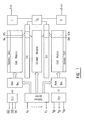
- Figure 1 is a block diagram illustrating a conventional semiconductor memory system; in particular Figure 1 outlines the overall structure of a dynamic RAM comprising memory cells each of which is composed of one transistor and one capacitor.
- SUP is a power supply circuit which receives a variety of power source voltages V DD , V ss , V BB from circuits external of the RAM and supplies them to the circuits internal of the RAM.
- CLG is the internal clock generator which receives a row address signal RAS, a column select signal CAS and a write enable signal WE from external circuits and supplies predetermined clock signals to internal circuits.
- sense amplifiers SA and column decoders connected to bit line pairs Bn, Bn' and Bm, Bm' etc., and row decoders connected to word lines, which word lines extend in a direction perpendicular to that of the bit line pairs, are arranged.
- a sense amplifier senses the content of the cell by comparing a bit line Bn connected to the cell and another bit line Bn' connected to a dummy cell. Thereby data is read as output information D out from an output buffer 0 via an input-output circuit I/O. Namely, sense amplifiers are provided in correspondence to respective bit line pairs.
- D in represents input information which can be input to a memory cell via input buffer and input-output circuit I/O.
- the memory cell matrix is improved to offer higher integration density by further reducing memory cell size.
- the dimensions of the bit line pairs and the sense amplifiers are not equal, and as indicated in Figure 1, sense amplifiers arranged in a line cannot be accommodated within the lateral extent of the memory cell matrix area as seen in the Figure. Therefore, the portions of the bit lines which extend for connection with the sense amplifiers spread out in the form of a fan, resulting in inefficient use of area. This contradicts the purpose of realisation of high integration density.
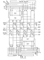
- Figure 2 is a schematic diagram showing parts of a memory system embodying the present invention.
- B 1 , B 1 ' to B 4 , 8 4 ' are bit line pairs
- SA1 to SA4 are sense amplifiers.
- WD1 and WD2 are word lines
- DWD and DWD' are dummy word lines
- DCP and DCP' are signal lines for discharging dummy cells.
- the bit line pairs are connected to bus lines via gate transistors, e.g. T1, T1' and T2, T2', which are turned ON and OFF under control of column decoders.
- V DD and V ss are high level and low level power supply lines respectively
- PC indicates a precharge signal line
- ⁇ 1 indicates an interrupt signal line
- ⁇ 2 indicates a latch signal line. Such lines are connected to each sense amplifier.
- the bus lines are connected to input-output circuits I/O, MA, via transistor pairs which are turned ON and OFF under the control of a signal IO, I/O.
- each memory cell consists of a transistor and a capacitor.
- Each dummy cell consists of a transistor, capacitor, and a discharging transistor.
- bit line pairs 8 1 , B 1 ' to B 4 , 8 4 ' are led out to opposite sides of the memory matrix, two bit line pairs being led out to each side, while two sense amplifiers SA1, SA2 are arranged on one side of the memory matrix and another two sense amplifiers SA3, SA4 are arranged on the other side of the memory matrix, along the direction of bit line pairs 8 1 , B 1 '; B 2 , 8 2 '; and B 3 , B 3 '; 8 4 , 8 4 '.
- each sense amplifier SA1 to SA4 is equal to the width of two bit line pairs, and the portions of bit lines which extend to those sense amplifiers are arranged so as to pass the sides of the sense amplifiers. That is, the bit line portions extending to amplifier SA3, for example, pass to the side of amplifier SA4, which is nearer to the memory matrix.
- the sense amplifiers SA1, SA2 are formed in an area on a side of the memory matrix into which the bit line pairs B 3 , B 3 ' and B 4 , B 4 ' are not led, while the sense amplifiers SA3, SA4 are formed in an area on a side of the memory matrix into which the bit line pairs 8 1 , 8 1 ' and B 2 , 8 2 ' are not led, and the portions of the bit line pairs B 3 , B 3 ' and B z , 8 2 ' for example, leading to sense amplifiers are connected to the sense amplifiers and pass to the side of the sense amplifiers SA1, SA4 and do not cross the sense amplifiers SA1, SA4.
- the number of bit line pairs and the number of sense amplifiers can be determined in general as follows.
- a value of m is obtained such that the width of m pairs of bit lines is approximately equal to the width of one sense amplifier, many bit line pairs are divided into blocks each consisting of 2m bit line pairs each, 2m sense amplifiers are provided for each block with m sense amplifiers to one side of the memory matrix in the bit line direction, and m sense amplifiers to the other side of the memory matrix, the m sense amplifiers on opposite sides of the memory matrix being disposed within a width equal to m bit line pairs.
- the arrangement as shown in Figure 2 can be obtained by establishing required connections.
- the embodiment described above is adapted to a memory system of the folded bit line type, where bit line pairs are provided in parallel (the lines of the pair run alongside one another).
- the present invention has been explained on the basis of its application to the relationship between bit line pairs and sense amplifiers.
- the present invention can naturally be adapted for application to the relationship between word lines or word line pairs, or bit lines or bit line pairs and decoder circuits, such as row or column decoders and between word lines or word line pairs or bit lines or bit line pairs and any other peripheral circuits, such as word decoder circuits for selecting and driving word lines or word line pairs, connected thereto.
- the present invention has the advantage that the word lines or bit lines of a highly integrated memory matrix and peripheral circuits in a peripheral circuit block such as an address decoder, sense amplifiers etc. can be connected without complicating the overall structure and with efficient use of area.
- An embodiment of the present invention relates to a semiconductor memory system having a memory matrix area wherein many word lines and bit lines cross mutually in row and column directions and memory cells are arranged at the intersections of the word lines and bit lines with high integration density.
- a plurality of peripheral circuit blocks which are connected to a plurality of adjacent word lines and bit lines, for example, blocks providing sense amplifiers and decoder circuits, are sequentially arranged in files against the direction of the bit lines or word lines, respectively. Thereby, connections between the word lines or bit lines and peripheral circuits can be made without complicating the structure, and with effective use of areas.
- the present invention provides a semiconductor memory device providing the memory matrix area comprising plurality of wirings or wiring pairs crossed in both row and column directions and the memory cells arranged in the intersection thereof, wherein a plurality of peripheral circuit blocks connected to the adjacent plurality of wirings or wiring pairs in the predetermined number are sequentially arranged in the same direction as said wiring in such a manner that at least a pair of said peripheral circuit block is arranged in files, and said wirings extended from said memory matrix area are connected to said peripheral circuit blocks.
Landscapes
- Engineering & Computer Science (AREA)
- Microelectronics & Electronic Packaging (AREA)
- Computer Hardware Design (AREA)
- Dram (AREA)
- Semiconductor Memories (AREA)
Claims (6)
Applications Claiming Priority (2)
| Application Number | Priority Date | Filing Date | Title |
|---|---|---|---|
| JP16207979A JPS5683891A (en) | 1979-12-13 | 1979-12-13 | Semiconductor storage device |
| JP162079/79 | 1979-12-13 |
Related Child Applications (1)
| Application Number | Title | Priority Date | Filing Date |
|---|---|---|---|
| EP85101832.5 Division-Into | 1980-12-11 |
Publications (3)
| Publication Number | Publication Date |
|---|---|
| EP0031659A2 EP0031659A2 (de) | 1981-07-08 |
| EP0031659A3 EP0031659A3 (en) | 1981-07-15 |
| EP0031659B1 true EP0031659B1 (de) | 1986-05-14 |
Family
ID=15747680
Family Applications (2)
| Application Number | Title | Priority Date | Filing Date |
|---|---|---|---|
| EP85101832A Expired - Lifetime EP0155521B1 (de) | 1979-12-13 | 1980-12-11 | Halbleiterspeicheranordnung |
| EP80304461A Expired EP0031659B1 (de) | 1979-12-13 | 1980-12-11 | Halbleiterspeichervorrichtung mit einer Speichermatrixfläche und mehreren Randschaltungen |
Family Applications Before (1)
| Application Number | Title | Priority Date | Filing Date |
|---|---|---|---|
| EP85101832A Expired - Lifetime EP0155521B1 (de) | 1979-12-13 | 1980-12-11 | Halbleiterspeicheranordnung |
Country Status (4)
| Country | Link |
|---|---|
| US (1) | US4418399A (de) |
| EP (2) | EP0155521B1 (de) |
| JP (1) | JPS5683891A (de) |
| DE (2) | DE3072204T2 (de) |
Families Citing this family (15)
| Publication number | Priority date | Publication date | Assignee | Title |
|---|---|---|---|---|
| JPS6059677B2 (ja) * | 1981-08-19 | 1985-12-26 | 富士通株式会社 | 半導体記憶装置 |
| US4750154A (en) * | 1984-07-10 | 1988-06-07 | Prime Computer, Inc. | Memory alignment system and method |
| BR8503161A (pt) * | 1984-07-31 | 1986-03-25 | Int Standard Electric Corp | Metodo para investigar uma matriz de associacao |
| US4979145A (en) * | 1986-05-01 | 1990-12-18 | Motorola, Inc. | Structure and method for improving high speed data rate in a DRAM |
| JPH088304B2 (ja) * | 1987-08-19 | 1996-01-29 | 富士通株式会社 | 半導体集積回路装置及びその設計方法 |
| US5016216A (en) * | 1988-10-17 | 1991-05-14 | Waferscale Integration, Inc. | Decoder for a floating gate memory |
| JPH0775116B2 (ja) * | 1988-12-20 | 1995-08-09 | 三菱電機株式会社 | 半導体記憶装置 |
| JPH081946B2 (ja) * | 1990-01-26 | 1996-01-10 | 株式会社東芝 | 半導体集積回路 |
| JP2982920B2 (ja) * | 1990-07-10 | 1999-11-29 | 三菱電機株式会社 | 半導体記憶装置 |
| JPH0562461A (ja) * | 1991-04-09 | 1993-03-12 | Mitsubishi Electric Corp | 半導体記憶装置 |
| KR940007639B1 (ko) * | 1991-07-23 | 1994-08-22 | 삼성전자 주식회사 | 분할된 입출력 라인을 갖는 데이타 전송회로 |
| JP3183541B2 (ja) * | 1991-10-22 | 2001-07-09 | シャープ株式会社 | 半導体記憶装置 |
| JPH08172169A (ja) * | 1994-12-16 | 1996-07-02 | Toshiba Microelectron Corp | 半導体記憶装置 |
| JPH10303387A (ja) * | 1997-04-28 | 1998-11-13 | Mitsubishi Electric Corp | 半導体記憶装置 |
| DE602005006791D1 (de) * | 2005-07-28 | 2008-06-26 | St Microelectronics Srl | Halbleiterspeicher und sein Seitenpufferspeicher mit verbessertem Layout |
Family Cites Families (13)
| Publication number | Priority date | Publication date | Assignee | Title |
|---|---|---|---|---|
| US3814846A (en) * | 1972-01-20 | 1974-06-04 | Reticon Corp | High density photodetection array |
| US3909808A (en) * | 1974-12-23 | 1975-09-30 | Ibm | Minimum pitch mosfet decoder circuit configuration |
| JPS5539073B2 (de) * | 1974-12-25 | 1980-10-08 | ||
| JPS51113545A (en) * | 1975-03-31 | 1976-10-06 | Hitachi Ltd | Memory |
| DE2557165C3 (de) * | 1975-12-18 | 1979-01-18 | Siemens Ag, 1000 Berlin Und 8000 Muenchen | Decoderschaltung und ihre Anordnung zur Integrierung auf einem Halbleiterbaustein |
| US4156938A (en) * | 1975-12-29 | 1979-05-29 | Mostek Corporation | MOSFET Memory chip with single decoder and bi-level interconnect lines |
| US4045783A (en) * | 1976-04-12 | 1977-08-30 | Standard Microsystems Corporation | Mos one transistor cell ram having divided and balanced bit lines, coupled by regenerative flip-flop sense amplifiers, and balanced access circuitry |
| JPS5349969A (en) * | 1976-10-18 | 1978-05-06 | Hitachi Ltd | Semiconductor memory unit |
| DE2647394C2 (de) * | 1976-10-20 | 1978-11-16 | Siemens Ag, 1000 Berlin Und 8000 Muenchen | MOS-Halbleiterspeicherbaustein |
| DE2746336A1 (de) * | 1977-10-14 | 1979-04-19 | Siemens Ag | Dynamischer halbleiterspeicher mit einer matrix aus ein-transistor-speicherzellen |
| US4160275A (en) * | 1978-04-03 | 1979-07-03 | International Business Machines Corporation | Accessing arrangement for memories with small cells |
| DE2919166C2 (de) * | 1978-05-12 | 1986-01-02 | Nippon Electric Co., Ltd., Tokio/Tokyo | Speichervorrichtung |
| JPS5542344A (en) * | 1978-09-21 | 1980-03-25 | Toshiba Corp | Mos type dynamic memory unit |
-
1979
- 1979-12-13 JP JP16207979A patent/JPS5683891A/ja active Granted
-
1980
- 1980-12-11 EP EP85101832A patent/EP0155521B1/de not_active Expired - Lifetime
- 1980-12-11 DE DE8585101832T patent/DE3072204T2/de not_active Expired - Fee Related
- 1980-12-11 DE DE8080304461T patent/DE3071607D1/de not_active Expired
- 1980-12-11 EP EP80304461A patent/EP0031659B1/de not_active Expired
- 1980-12-15 US US06/216,674 patent/US4418399A/en not_active Expired - Lifetime
Also Published As
| Publication number | Publication date |
|---|---|
| JPS5683891A (en) | 1981-07-08 |
| DE3071607D1 (en) | 1986-06-19 |
| EP0031659A3 (en) | 1981-07-15 |
| EP0155521A3 (en) | 1988-12-14 |
| US4418399A (en) | 1983-11-29 |
| EP0155521B1 (de) | 1992-11-11 |
| DE3072204T2 (de) | 1993-03-25 |
| EP0155521A2 (de) | 1985-09-25 |
| JPS6155198B2 (de) | 1986-11-26 |
| DE3072204D1 (de) | 1992-12-17 |
| EP0031659A2 (de) | 1981-07-08 |
Similar Documents
| Publication | Publication Date | Title |
|---|---|---|
| EP0031659B1 (de) | Halbleiterspeichervorrichtung mit einer Speichermatrixfläche und mehreren Randschaltungen | |
| EP0170052B1 (de) | Halbleiterschaltungsanordnung in Hauptscheibentechnik | |
| US6404661B2 (en) | Semiconductor storage device having arrangement for controlling activation of sense amplifiers | |
| EP0096359A2 (de) | Halbleiterspeicheranordnung | |
| KR100240538B1 (ko) | 반도체 기억 장치 | |
| KR970067852A (ko) | 반도체 집적회로장치 | |
| EP0225499A2 (de) | Saat- und Stichverfahren zu integrierten Feldanordnungen | |
| JPH0772991B2 (ja) | 半導体記憶装置 | |
| US5263002A (en) | Semiconductor memory device and its topography | |
| US6448602B1 (en) | Semiconductor memory device with improved arrangement of memory blocks and peripheral circuits | |
| US4779227A (en) | Semiconductor memory device | |
| CA1232354A (en) | Semiconductor memory | |
| US5671188A (en) | Random access memory having selective intra-bank fast activation of sense amplifiers | |
| KR920010632A (ko) | 반도체 메모리 디바이스 | |
| US6678204B2 (en) | Semiconductor memory device with high-speed operation and methods of using and designing thereof | |
| US5579264A (en) | Distributed signal drivers in arrayable devices | |
| KR0140213Y1 (ko) | 반도체 기억장치 | |
| US5535153A (en) | Semiconductor device | |
| US5375097A (en) | Segmented bus architecture for improving speed in integrated circuit memories | |
| US6458644B1 (en) | Data bus architecture for integrated circuit devices having embedded dynamic random access memory (DRAM) with a large aspect ratio providing reduced capacitance and power requirements | |
| JPS59217290A (ja) | 半導体メモリ | |
| JP3469074B2 (ja) | 半導体メモリ装置 | |
| JPH06259968A (ja) | 半導体記憶装置 | |
| JPH036596B2 (de) | ||
| JP3020614B2 (ja) | 半導体記憶装置 |
Legal Events
| Date | Code | Title | Description |
|---|---|---|---|
| PUAI | Public reference made under article 153(3) epc to a published international application that has entered the european phase |
Free format text: ORIGINAL CODE: 0009012 |
|
| PUAL | Search report despatched |
Free format text: ORIGINAL CODE: 0009013 |
|
| AK | Designated contracting states |
Designated state(s): AT BE CH DE FR GB IT LU NL SE |
|
| AK | Designated contracting states |
Designated state(s): DE FR GB NL |
|
| RBV | Designated contracting states (corrected) |
Designated state(s): DE FR GB NL |
|
| 17P | Request for examination filed |
Effective date: 19810909 |
|
| RBV | Designated contracting states (corrected) |
Designated state(s): DE FR GB |
|
| GRAA | (expected) grant |
Free format text: ORIGINAL CODE: 0009210 |
|
| STAA | Information on the status of an ep patent application or granted ep patent |
Free format text: STATUS: THE PATENT HAS BEEN GRANTED |
|
| AK | Designated contracting states |
Kind code of ref document: B1 Designated state(s): DE FR GB |
|
| REF | Corresponds to: |
Ref document number: 3071607 Country of ref document: DE Date of ref document: 19860619 |
|
| ET | Fr: translation filed | ||
| PLBE | No opposition filed within time limit |
Free format text: ORIGINAL CODE: 0009261 |
|
| 26N | No opposition filed | ||
| PGFP | Annual fee paid to national office [announced via postgrant information from national office to epo] |
Ref country code: FR Payment date: 19981209 Year of fee payment: 19 |
|
| PGFP | Annual fee paid to national office [announced via postgrant information from national office to epo] |
Ref country code: GB Payment date: 19981211 Year of fee payment: 19 |
|
| PGFP | Annual fee paid to national office [announced via postgrant information from national office to epo] |
Ref country code: DE Payment date: 19981221 Year of fee payment: 19 |
|
| PG25 | Lapsed in a contracting state [announced via postgrant information from national office to epo] |
Ref country code: GB Free format text: LAPSE BECAUSE OF NON-PAYMENT OF DUE FEES Effective date: 19991211 |
|
| GBPC | Gb: european patent ceased through non-payment of renewal fee |
Effective date: 19991211 |
|
| PG25 | Lapsed in a contracting state [announced via postgrant information from national office to epo] |
Ref country code: FR Free format text: LAPSE BECAUSE OF NON-PAYMENT OF DUE FEES Effective date: 20000831 |
|
| PG25 | Lapsed in a contracting state [announced via postgrant information from national office to epo] |
Ref country code: DE Free format text: LAPSE BECAUSE OF NON-PAYMENT OF DUE FEES Effective date: 20001003 |
|
| REG | Reference to a national code |
Ref country code: FR Ref legal event code: ST |