EP0020995A1 - Procédé et circuit sélection et de décharge des capacités de lignes de bit d'une mémoire MTL à semi-conducteurs à haute intégration - Google Patents
Procédé et circuit sélection et de décharge des capacités de lignes de bit d'une mémoire MTL à semi-conducteurs à haute intégration Download PDFInfo
- Publication number
- EP0020995A1 EP0020995A1 EP80102653A EP80102653A EP0020995A1 EP 0020995 A1 EP0020995 A1 EP 0020995A1 EP 80102653 A EP80102653 A EP 80102653A EP 80102653 A EP80102653 A EP 80102653A EP 0020995 A1 EP0020995 A1 EP 0020995A1
- Authority
- EP
- European Patent Office
- Prior art keywords
- read
- memory cells
- bit line
- write
- discharge
- Prior art date
- Legal status (The legal status is an assumption and is not a legal conclusion. Google has not performed a legal analysis and makes no representation as to the accuracy of the status listed.)
- Granted
Links
Images


Classifications
-
- G—PHYSICS
- G11—INFORMATION STORAGE
- G11C—STATIC STORES
- G11C11/00—Digital stores characterised by the use of particular electric or magnetic storage elements; Storage elements therefor
- G11C11/21—Digital stores characterised by the use of particular electric or magnetic storage elements; Storage elements therefor using electric elements
- G11C11/34—Digital stores characterised by the use of particular electric or magnetic storage elements; Storage elements therefor using electric elements using semiconductor devices
- G11C11/40—Digital stores characterised by the use of particular electric or magnetic storage elements; Storage elements therefor using electric elements using semiconductor devices using transistors
- G11C11/41—Digital stores characterised by the use of particular electric or magnetic storage elements; Storage elements therefor using electric elements using semiconductor devices using transistors forming static cells with positive feedback, i.e. cells not needing refreshing or charge regeneration, e.g. bistable multivibrator or Schmitt trigger
- G11C11/411—Digital stores characterised by the use of particular electric or magnetic storage elements; Storage elements therefor using electric elements using semiconductor devices using transistors forming static cells with positive feedback, i.e. cells not needing refreshing or charge regeneration, e.g. bistable multivibrator or Schmitt trigger using bipolar transistors only
- G11C11/4113—Digital stores characterised by the use of particular electric or magnetic storage elements; Storage elements therefor using electric elements using semiconductor devices using transistors forming static cells with positive feedback, i.e. cells not needing refreshing or charge regeneration, e.g. bistable multivibrator or Schmitt trigger using bipolar transistors only with at least one cell access to base or collector of at least one of said transistors, e.g. via access diodes, access transistors
-
- G—PHYSICS
- G11—INFORMATION STORAGE
- G11C—STATIC STORES
- G11C11/00—Digital stores characterised by the use of particular electric or magnetic storage elements; Storage elements therefor
- G11C11/21—Digital stores characterised by the use of particular electric or magnetic storage elements; Storage elements therefor using electric elements
- G11C11/34—Digital stores characterised by the use of particular electric or magnetic storage elements; Storage elements therefor using electric elements using semiconductor devices
- G11C11/40—Digital stores characterised by the use of particular electric or magnetic storage elements; Storage elements therefor using electric elements using semiconductor devices using transistors
- G11C11/401—Digital stores characterised by the use of particular electric or magnetic storage elements; Storage elements therefor using electric elements using semiconductor devices using transistors forming cells needing refreshing or charge regeneration, i.e. dynamic cells
- G11C11/402—Digital stores characterised by the use of particular electric or magnetic storage elements; Storage elements therefor using electric elements using semiconductor devices using transistors forming cells needing refreshing or charge regeneration, i.e. dynamic cells with charge regeneration individual to each memory cell, i.e. internal refresh
- G11C11/4023—Digital stores characterised by the use of particular electric or magnetic storage elements; Storage elements therefor using electric elements using semiconductor devices using transistors forming cells needing refreshing or charge regeneration, i.e. dynamic cells with charge regeneration individual to each memory cell, i.e. internal refresh using field effect transistors
-
- G—PHYSICS
- G11—INFORMATION STORAGE
- G11C—STATIC STORES
- G11C11/00—Digital stores characterised by the use of particular electric or magnetic storage elements; Storage elements therefor
- G11C11/21—Digital stores characterised by the use of particular electric or magnetic storage elements; Storage elements therefor using electric elements
- G11C11/34—Digital stores characterised by the use of particular electric or magnetic storage elements; Storage elements therefor using electric elements using semiconductor devices
- G11C11/40—Digital stores characterised by the use of particular electric or magnetic storage elements; Storage elements therefor using electric elements using semiconductor devices using transistors
- G11C11/41—Digital stores characterised by the use of particular electric or magnetic storage elements; Storage elements therefor using electric elements using semiconductor devices using transistors forming static cells with positive feedback, i.e. cells not needing refreshing or charge regeneration, e.g. bistable multivibrator or Schmitt trigger
- G11C11/413—Auxiliary circuits, e.g. for addressing, decoding, driving, writing, sensing, timing or power reduction
- G11C11/414—Auxiliary circuits, e.g. for addressing, decoding, driving, writing, sensing, timing or power reduction for memory cells of the bipolar type
- G11C11/416—Read-write [R-W] circuits
Definitions
- the invention relates to a method according to the preamble of claim 1 and a circuit arrangement for performing the method.
- bipolar transistors are characterized by short switching times and are particularly suitable for the construction of extremely highly integrated memories and logic circuit groups.
- Memories that are constructed with memory cells made of bipolar transistors that have an MTL-like structure require the reloading of bit data and / or control line capacities in order to select a memory cell.
- the voltage swing of the bit lines corresponds approximately to the voltage swing of the selected word lines.
- the capacitive discharge currents are dissipated to ground via the memory cells of the selected word line and via the word line driver.
- this has the disadvantage that the area requirement of the driver circuits, the electrical power loss for each driver and the delay time in the selection of the word line become disproportionately large, so that the advantages of the MTL structure used thereby become again would be destroyed.
- the circuit arrangement mentioned is characterized in that the bit lines within the memory matrix are connected to a discharge line, which in turn is connected to a discharge circuit, and that the discharge circuit and all word and / or bit line switching transistors for control via lines are connected to a control or control logic , which is controlled with the selection signal of the memory chip.
- the number of components required in the peripheral circuits of such a memory is still very high.
- the read signal supplied is dependent on the direct current supplied by the read / write amplifier.
- the invention is therefore based on the object, a Ver drive to read and / or write to create an integrated semiconductor memory, the memory cells are designed in particular in MTL technology, which are arranged at crossing points of word and bit lines and are selected via drivers and decoders, the higher and steeper read and write signal with a reduction in the components in the read and write circuits and a reduction in the required control lines, and to create a circuit arrangement for carrying out the method.
- the advantage of the method according to the invention is the substantial improvement of the read signal, which is characterized by a significantly higher slope and absolute size.
- the number of components in the read / write circuit associated with each pair of bit lines is significantly reduced since no components are required to provide a sense and / or write direct current.
- the number of drive lines for the components within the read / write circuit is reduced significantly.
- Interfering injection currents due to the isolation between selected and unselected cells are significantly reduced because the new circuit works with lower currents.
- the tension level on the read / write and bit lines the new read / write circuit is extremely uncritical, since the two transistors still available for writing never turn on inversely, due to the fact that they are blocked by Schottky diodes.
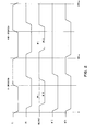
- the circuit diagram shown in FIG. 1 represents a section of a memory level in integrated technology.
- the new read / write amplifier is shown in the lower part of the circuit arrangement. It consists of the two Schottky-clamped transistors T46 and T49 with the Schottky collector contacts S46 and S49.
- the base of transistor T46 is connected to a line WT1 which is common to all read / write amplifiers of a memory level and the base of transistor T49 is connected to a line WTO which is also common to all read / write amplifiers of a memory level .
- the bases of the two transistors T46 and T49 are connected via a common line to a bit selection line BS, which is connected to the base of one bit switch T51 via two Schottky diodes D50 and D51 connected in series.
- This transistor T51 which represents the bit switch for the bit line BL1
- the transistor T50 is connected to the bit line BL1
- the transistor T50 to the bit line BLO
- the other electrode is both connected to a bit reference line BRL at the memory level.
- the bases of both transistors T50 and T51 are supplied with a current via a resistor R50, which is connected to a further reference line BRBL, which keeps these transistors saturated during the idle period.
- word lines WL are present in FIG. 1 for each memory cell CO, 1, ..., of which, however, only the word lines WLO and WL1 for the memory cells CO and C1 are shown in this circuit diagram.
- a known differential amplifier not shown, is connected to the bit lines BLO and BL1 for sensing the stored information and is common to all cells within a bit line pair BLO, BL1.
- the task of the Schottky diodes D50, D51 and the resistor R50 is to prepare and set the rest and operating potentials during the individual memory operations in a known manner.
- the currents for the bit lines BLO and BL1 are supplied via the transistors T50 and T51 serving as bit line switches. These two transistors T50 and T51 are operated inversely and deeply saturated, which ensures that the bit line potentials VBLO and VBL1 differ from each other only by a small amount (typically 3 mV for a stored bit pattern under the most critical conditions).
- the word line potentials VWLO, VWL1, ..., VWL (N-1) are VBE (typically 600 mV) below the bit line potential.
- the memory cell CLO shown in FIG. 1 is to be selected for subsequent reading.
- the bit-side selection of the memory cell CO takes place by pulling down the potential on the line BS (see time diagram according to FIG. 2).
- the two transistors T50 and T51 serving as bit line switches are switched off and the quiescent current is interrupted.
- the memory cell CO in FIG. 1 is selected on the word side by lowering the potential on the word line WLO.
- a charge .DELTA.Q flows in a pulsed manner into the two input capacitances CEOO and CE01, as a result of which the injector voltages of the selected memory cell CO increase. Analyzes in practical tests showed that with a word line swing of recharging the injector capacity with an increase in injector voltages results.
- the discharge currents injected from the injector capacities CEOO and CE01 to the inner cell nodes cause the capacitors CCOO and CC01 to be charged.
- the base-emitter voltage of both NPN transistors T02 and T03 increases.
- the transistor T02 the voltage reaches a value of approximately 400 mV for a short time, starting from approximately 20 mV, after which it drops again very quickly when the base-emitter Capacitance CC01 of transistor T03 is charged to such an extent that the discharge current increases the side of the memory cell CO which is in the off state can be taken over.
- the read signal results from the different degradation of the charges on the side of the memory cell CO that is in the off state and that in the on state.
- the discharge current on the side in the off state is the collector current of the NPN transistor T03 in the on state. This discharge is very quick.
- On the side in the on state corresponds to that of the base current of the NPN transistor T03 in the on state. This is lower than the collector current by the current gain ⁇ u.
- the part of ⁇ Q which is not discharged by the base current remains as a storage charge in the PNP transistor TO1 on the side which is in the on state. This part falls with the storage time constant T S, which is typically 30 ns.
- the larger charge on the side in the on state corresponds to a higher injector voltage.
- one of the two transistors T46 or T49 present in the read / write circuit is activated, i.e. put in the on state.
- the bit line BLO is discharged when the transistor T46 is turned on and the bit line BLO is discharged when the transistor T49 is in the on state.
- the charge Q is formed on the respective input capacitance of the memory cell CO connected to the bit line BLO or BL1, as when reading when the word line potential VWLO is lowered. If, at this point in time, the transistor that was previously in the on state can no longer take over the current flowing into the collector because the PNP transistor integrated with it no longer supplies a base current, the memory cell topples over to the other state, ie The desired binary zero or binary one is entered.
- driver and decoder circuits on the bit and word sides of the memory, respectively, are neither shown nor described because they are well known in the art and are not necessary to explain the present invention.
Landscapes
- Engineering & Computer Science (AREA)
- Microelectronics & Electronic Packaging (AREA)
- Computer Hardware Design (AREA)
- Static Random-Access Memory (AREA)
Applications Claiming Priority (2)
| Application Number | Priority Date | Filing Date | Title |
|---|---|---|---|
| DE2926050 | 1979-06-28 | ||
| DE2926050A DE2926050C2 (de) | 1979-06-28 | 1979-06-28 | Verfahren und Schaltungsanordnung zum Lesen Und/oder Schreiben eines integrierten Halbleiterspeichers mit Speicherzellen in MTL-Technik |
Publications (2)
| Publication Number | Publication Date |
|---|---|
| EP0020995A1 true EP0020995A1 (fr) | 1981-01-07 |
| EP0020995B1 EP0020995B1 (fr) | 1983-06-15 |
Family
ID=6074350
Family Applications (1)
| Application Number | Title | Priority Date | Filing Date |
|---|---|---|---|
| EP80102653A Expired EP0020995B1 (fr) | 1979-06-28 | 1980-05-13 | Procédé et circuit sélection et de décharge des capacités de lignes de bit d'une mémoire MTL à semi-conducteurs à haute intégration |
Country Status (5)
| Country | Link |
|---|---|
| US (1) | US4330853A (fr) |
| EP (1) | EP0020995B1 (fr) |
| JP (1) | JPS5824875B2 (fr) |
| DE (2) | DE2926050C2 (fr) |
| IT (1) | IT1174672B (fr) |
Cited By (3)
| Publication number | Priority date | Publication date | Assignee | Title |
|---|---|---|---|---|
| EP0031462A2 (fr) * | 1979-12-27 | 1981-07-08 | International Business Machines Corporation | Système de détection différentielle de charge pour un dispositif à 4 composants formant une cellule de mémoire MTL |
| EP0069227A2 (fr) * | 1981-07-06 | 1983-01-12 | International Business Machines Corporation | Mémoire semi-conductrice intégrée et méthode d'accès et de lecture |
| EP0078335A1 (fr) * | 1981-10-30 | 1983-05-11 | Ibm Deutschland Gmbh | Procédé de lecture d'une mémoire à semi-conducteurs |
Families Citing this family (8)
| Publication number | Priority date | Publication date | Assignee | Title |
|---|---|---|---|---|
| US4601016A (en) * | 1983-06-24 | 1986-07-15 | Honeywell Inc. | Semiconductor memory cell |
| US4578779A (en) * | 1984-06-25 | 1986-03-25 | International Business Machines Corporation | Voltage mode operation scheme for bipolar arrays |
| US4598390A (en) * | 1984-06-25 | 1986-07-01 | International Business Machines Corporation | Random access memory RAM employing complementary transistor switch (CTS) memory cells |
| US4596002A (en) * | 1984-06-25 | 1986-06-17 | International Business Machines Corporation | Random access memory RAM employing complementary transistor switch (CTS) memory cells |
| US4752913A (en) * | 1986-04-30 | 1988-06-21 | International Business Machines Corporation | Random access memory employing complementary transistor switch (CTS) memory cells |
| EP0246371B1 (fr) * | 1986-05-22 | 1991-01-09 | International Business Machines Corporation | Circuit de sortie pour logique intégrée à injection |
| US4763026A (en) * | 1987-04-09 | 1988-08-09 | National Semiconductor Corporation | Sense amplifier for single-ended data sensing |
| US5526319A (en) * | 1995-01-31 | 1996-06-11 | International Business Machines Corporation | Memory with adiabatically switched bit lines |
Citations (11)
| Publication number | Priority date | Publication date | Assignee | Title |
|---|---|---|---|---|
| US3540010A (en) * | 1968-08-27 | 1970-11-10 | Bell Telephone Labor Inc | Diode-coupled semiconductive memory |
| US3541531A (en) * | 1967-02-07 | 1970-11-17 | Bell Telephone Labor Inc | Semiconductive memory array wherein operating power is supplied via information paths |
| US3688264A (en) * | 1970-09-18 | 1972-08-29 | Rca Corp | Operation of field-effect transistor circuits having substantial distributed capacitance |
| US3736574A (en) * | 1971-12-30 | 1973-05-29 | Ibm | Pseudo-hierarchy memory system |
| US3786442A (en) * | 1972-02-24 | 1974-01-15 | Cogar Corp | Rapid recovery circuit for capacitively loaded bit lines |
| US3900838A (en) * | 1973-02-27 | 1975-08-19 | Ibm | Hybrid storage circuit |
| US4070656A (en) * | 1975-12-17 | 1978-01-24 | International Business Machines Corporation | Read/write speed up circuit for integrated data memories |
| US4090255A (en) * | 1975-03-15 | 1978-05-16 | International Business Machines Corporation | Circuit arrangement for operating a semiconductor memory system |
| US4112511A (en) * | 1977-09-13 | 1978-09-05 | Signetics Corporation | Four transistor static bipolar memory cell using merged transistors |
| EP0004871A1 (fr) * | 1978-04-19 | 1979-10-31 | International Business Machines Corporation | Dispositif semi-conducteur intégré monolithiquement avec au moins une structure I2L, cellule de mémoire utilisant un tel dispositif et matrice de mémoire utilisant une telle cellule de mémoire |
| EP0013302A1 (fr) * | 1978-12-22 | 1980-07-23 | International Business Machines Corporation | Procédé et circuit de commande d'une mémoire intégrée à semi-conducteurs |
Family Cites Families (12)
| Publication number | Priority date | Publication date | Assignee | Title |
|---|---|---|---|---|
| US3815106A (en) * | 1972-05-11 | 1974-06-04 | S Wiedmann | Flip-flop memory cell arrangement |
| US3668264A (en) * | 1969-07-15 | 1972-06-06 | Union Oil Co | Production of alkylbenzenes |
| US3643231A (en) * | 1970-04-20 | 1972-02-15 | Ibm | Monolithic associative memory cell |
| DE2021824C3 (de) * | 1970-05-05 | 1980-08-14 | Ibm Deutschland Gmbh, 7000 Stuttgart | Monolithische Halbleiterschaltung |
| US3816758A (en) * | 1971-04-14 | 1974-06-11 | Ibm | Digital logic circuit |
| US3816748A (en) * | 1972-04-28 | 1974-06-11 | Alpha Ind Inc | Ion accelerator employing crossed-field selector |
| US3786422A (en) * | 1973-01-31 | 1974-01-15 | Rel Reeves Inc | System for determination of deviations of a vehicle from a prescribed route |
| US3866531A (en) * | 1973-10-12 | 1975-02-18 | Sperry Rand Corp | Apparatus for controlling the movement of crop material in a roll forming machine |
| GB1494481A (en) * | 1973-12-21 | 1977-12-07 | Mullard Ltd | Electrical circuits comprising master/slave bistable arrangements |
| US4032902A (en) * | 1975-10-30 | 1977-06-28 | Fairchild Camera And Instrument Corporation | An improved semiconductor memory cell circuit and structure |
| US4021786A (en) * | 1975-10-30 | 1977-05-03 | Fairchild Camera And Instrument Corporation | Memory cell circuit and semiconductor structure therefore |
| JPS53117341A (en) * | 1977-03-24 | 1978-10-13 | Toshiba Corp | Semiconductor memory |
-
1979
- 1979-06-28 DE DE2926050A patent/DE2926050C2/de not_active Expired
-
1980
- 1980-04-03 US US06/136,859 patent/US4330853A/en not_active Expired - Lifetime
- 1980-05-09 JP JP55060778A patent/JPS5824875B2/ja not_active Expired
- 1980-05-13 DE DE8080102653T patent/DE3063756D1/de not_active Expired
- 1980-05-13 EP EP80102653A patent/EP0020995B1/fr not_active Expired
- 1980-06-06 IT IT22604/80A patent/IT1174672B/it active
Patent Citations (11)
| Publication number | Priority date | Publication date | Assignee | Title |
|---|---|---|---|---|
| US3541531A (en) * | 1967-02-07 | 1970-11-17 | Bell Telephone Labor Inc | Semiconductive memory array wherein operating power is supplied via information paths |
| US3540010A (en) * | 1968-08-27 | 1970-11-10 | Bell Telephone Labor Inc | Diode-coupled semiconductive memory |
| US3688264A (en) * | 1970-09-18 | 1972-08-29 | Rca Corp | Operation of field-effect transistor circuits having substantial distributed capacitance |
| US3736574A (en) * | 1971-12-30 | 1973-05-29 | Ibm | Pseudo-hierarchy memory system |
| US3786442A (en) * | 1972-02-24 | 1974-01-15 | Cogar Corp | Rapid recovery circuit for capacitively loaded bit lines |
| US3900838A (en) * | 1973-02-27 | 1975-08-19 | Ibm | Hybrid storage circuit |
| US4090255A (en) * | 1975-03-15 | 1978-05-16 | International Business Machines Corporation | Circuit arrangement for operating a semiconductor memory system |
| US4070656A (en) * | 1975-12-17 | 1978-01-24 | International Business Machines Corporation | Read/write speed up circuit for integrated data memories |
| US4112511A (en) * | 1977-09-13 | 1978-09-05 | Signetics Corporation | Four transistor static bipolar memory cell using merged transistors |
| EP0004871A1 (fr) * | 1978-04-19 | 1979-10-31 | International Business Machines Corporation | Dispositif semi-conducteur intégré monolithiquement avec au moins une structure I2L, cellule de mémoire utilisant un tel dispositif et matrice de mémoire utilisant une telle cellule de mémoire |
| EP0013302A1 (fr) * | 1978-12-22 | 1980-07-23 | International Business Machines Corporation | Procédé et circuit de commande d'une mémoire intégrée à semi-conducteurs |
Non-Patent Citations (6)
| Title |
|---|
| ELECTRONICS, Band 47, Nr. 9, 2. Mai 1974, Seiten 110-114 New York, U.S.A. GERSBACH: "Current Steering Simplifies and Shrinks 1k Bipolar RAM" * Seiten 112-114, Abschnitt: "A slightly different bit drive"; Figuren 1, 3, 4 * & US - A - 3 736 574 (I.B.M.). * |
| I.B.M. TECHNICAL DISCLOSURE BULLETIN, Band 21, Nr. 1, Juni 1978, Seiten 231-232 Armonk, U.S.A. WIEDMANN: "MTL Storage Cell". * |
| IBM TECHNICAL DISCLOSURE BULLETIN, Band 13, Nr. 6, November 1970, Seiten 1705-1706 Armonk, U.S.A. WIEDMANN et al.: "Restore Circuitry for Bit/Sense System" * Seiten 1705-1706 * * |
| IEEE JOURNAL OF SOLID-STATE CIRCUITS, Band SC13, Nr. 5, Oktober 1978, Seiten 656-663 New York, U.S.A. KAWARADA et al.: "A Fast 7.5 ns Access 1K-Bit RAM for Cache-Memory Systems" * Seiten 659-660, Abschnitt: "F. Error-Write Suppression and Bit Line Clamping"; Figuren 5-9 * * |
| IEEE JOURNAL OF SOLID-STATE CIRCUITS, Band SC2, Nr. 4, Dezember 1967, Seiten 196-201 New York, U.S.A. IWERSEN: "Beam-Lead Sealed-Junction Semiconductor Memory with Minimal Cell Complexity" & US - A - 3 541 531 (BELL). * |
| IEEE JOURNAL OF SOLID-STATE CIRCUITS, Band SC6, Nr. 5, Oktober 1971, Seiten 297-300 New York, U.S.A. HENN: "Bipolar Dynamic Memory Cell". * |
Cited By (5)
| Publication number | Priority date | Publication date | Assignee | Title |
|---|---|---|---|---|
| EP0031462A2 (fr) * | 1979-12-27 | 1981-07-08 | International Business Machines Corporation | Système de détection différentielle de charge pour un dispositif à 4 composants formant une cellule de mémoire MTL |
| EP0031462A3 (en) * | 1979-12-27 | 1981-08-05 | International Business Machines Corporation | Differential charge sensing system for an integrated memory using dual-capacitance cells coupled to two bit lines |
| EP0069227A2 (fr) * | 1981-07-06 | 1983-01-12 | International Business Machines Corporation | Mémoire semi-conductrice intégrée et méthode d'accès et de lecture |
| EP0069227A3 (en) * | 1981-07-06 | 1985-04-03 | International Business Machines Corporation | Integrated semiconductor memory and method for accessing and reading |
| EP0078335A1 (fr) * | 1981-10-30 | 1983-05-11 | Ibm Deutschland Gmbh | Procédé de lecture d'une mémoire à semi-conducteurs |
Also Published As
| Publication number | Publication date |
|---|---|
| DE2926050B1 (de) | 1981-01-08 |
| IT1174672B (it) | 1987-07-01 |
| DE3063756D1 (en) | 1983-07-21 |
| DE2926050C2 (de) | 1981-10-01 |
| EP0020995B1 (fr) | 1983-06-15 |
| US4330853A (en) | 1982-05-18 |
| IT8022604A0 (it) | 1980-06-06 |
| JPS567291A (en) | 1981-01-24 |
| JPS5824875B2 (ja) | 1983-05-24 |
Similar Documents
| Publication | Publication Date | Title |
|---|---|---|
| DE2659248C3 (de) | Dynamischer Speicher mit wahlfreiem Zugriff | |
| DE2556831C2 (de) | Matrixspeicher und Verfahren zu seinem Betrieb | |
| DE1499843B2 (de) | Anordnung mit mindestens einer Speicherzelle mit mehreren Transistoren | |
| DE2707456C3 (fr) | ||
| EP0020995B1 (fr) | Procédé et circuit sélection et de décharge des capacités de lignes de bit d'une mémoire MTL à semi-conducteurs à haute intégration | |
| DE2610881C2 (de) | Schneller Assoziativ-Speicher | |
| EP0013302B1 (fr) | Procédé et circuit de commande d'une mémoire intégrée à semi-conducteurs | |
| DE2429771A1 (de) | Speichermatrix mit steuerbaren vierschichthalbleitern | |
| DE3038641A1 (de) | Halbleiter-speicherschaltung | |
| DE2302137B2 (de) | Leseschaltung zum zerstörungsfreien Auslesen dynamischer Ladungs-Speicherzellen | |
| EP0078335B1 (fr) | Procédé de lecture d'une mémoire à semi-conducteurs | |
| DE3305427C2 (de) | Bipolarer Halbleiterspeicher | |
| EP0021143B1 (fr) | Procédé et circuit de sélection et de décharge des capacités de lignes de bit d'une mémoire à haute intégration à semi-conducteurs | |
| EP0031001B1 (fr) | Procédé pour l'amplification capacitive d'un signal de lecture dans une mémoire à semiconducteur intégrée avec des cellules de mémoire à technique MTL | |
| DE2152706B2 (de) | Monolithischer integrierter halbleiterspeicher fuer binaere daten | |
| DE2556833A1 (de) | Verfahren und schaltungsanordnung zum betreiben eines halbleiterspeichers | |
| EP0022930B1 (fr) | Circuit de recharge pour mémoire à semi-conducteurs | |
| EP0003030A2 (fr) | Cellule de mémoire dynamique bipolaire | |
| DE3938638A1 (de) | Halbleiterspeichereinrichtung mit einem verbesserten leseverstaerker vom stromtyp mit hoher betriebsgeschwindigkeit und verfahren zu dessen betreibung | |
| DE1774948B2 (de) | Wortorganisierter speicher | |
| DE1499843C (de) | Anordnung mit mindestens einer Spei cherzelle mit mehreren Transistoren | |
| DE2348065C3 (de) | Bipolarer Transistorspeicher mit kapazitiver Speicherung | |
| DE2002708C3 (de) | Speicheranordnung mit bistabilen Kippschaltungen | |
| DE1499857C (de) | Lese Treiber Schaltung für einen Datenspeicher | |
| DE3226923C1 (de) | Schaltungsanordnung zur Aufladung der Bitleitungen in einem statischen MOS-Speicher |
Legal Events
| Date | Code | Title | Description |
|---|---|---|---|
| PUAI | Public reference made under article 153(3) epc to a published international application that has entered the european phase |
Free format text: ORIGINAL CODE: 0009012 |
|
| AK | Designated contracting states |
Designated state(s): DE FR GB NL SE |
|
| 17P | Request for examination filed |
Effective date: 19810312 |
|
| GRAA | (expected) grant |
Free format text: ORIGINAL CODE: 0009210 |
|
| AK | Designated contracting states |
Designated state(s): DE FR GB NL SE |
|
| PG25 | Lapsed in a contracting state [announced via postgrant information from national office to epo] |
Ref country code: NL Effective date: 19830615 |
|
| REF | Corresponds to: |
Ref document number: 3063756 Country of ref document: DE Date of ref document: 19830721 |
|
| ET | Fr: translation filed | ||
| NLV1 | Nl: lapsed or annulled due to failure to fulfill the requirements of art. 29p and 29m of the patents act | ||
| PLBE | No opposition filed within time limit |
Free format text: ORIGINAL CODE: 0009261 |
|
| STAA | Information on the status of an ep patent application or granted ep patent |
Free format text: STATUS: NO OPPOSITION FILED WITHIN TIME LIMIT |
|
| PGFP | Annual fee paid to national office [announced via postgrant information from national office to epo] |
Ref country code: SE Payment date: 19840630 Year of fee payment: 5 |
|
| 26N | No opposition filed | ||
| PG25 | Lapsed in a contracting state [announced via postgrant information from national office to epo] |
Ref country code: SE Effective date: 19860514 |
|
| PGFP | Annual fee paid to national office [announced via postgrant information from national office to epo] |
Ref country code: GB Payment date: 19900404 Year of fee payment: 11 |
|
| PGFP | Annual fee paid to national office [announced via postgrant information from national office to epo] |
Ref country code: DE Payment date: 19900529 Year of fee payment: 11 |
|
| PGFP | Annual fee paid to national office [announced via postgrant information from national office to epo] |
Ref country code: FR Payment date: 19910430 Year of fee payment: 12 |
|
| PG25 | Lapsed in a contracting state [announced via postgrant information from national office to epo] |
Ref country code: GB Effective date: 19910513 |
|
| GBPC | Gb: european patent ceased through non-payment of renewal fee | ||
| PG25 | Lapsed in a contracting state [announced via postgrant information from national office to epo] |
Ref country code: DE Effective date: 19920303 |
|
| PG25 | Lapsed in a contracting state [announced via postgrant information from national office to epo] |
Ref country code: FR Effective date: 19930129 |
|
| REG | Reference to a national code |
Ref country code: FR Ref legal event code: ST |
|
| EUG | Se: european patent has lapsed |
Ref document number: 80102653.5 Effective date: 19870225 |