EP0016629B1 - System and method for restoring image signal levels and setting signal gain for image-viewing devices - Google Patents
System and method for restoring image signal levels and setting signal gain for image-viewing devices Download PDFInfo
- Publication number
- EP0016629B1 EP0016629B1 EP80300824A EP80300824A EP0016629B1 EP 0016629 B1 EP0016629 B1 EP 0016629B1 EP 80300824 A EP80300824 A EP 80300824A EP 80300824 A EP80300824 A EP 80300824A EP 0016629 B1 EP0016629 B1 EP 0016629B1
- Authority
- EP
- European Patent Office
- Prior art keywords
- signals
- video signals
- dark
- level
- output
- Prior art date
- Legal status (The legal status is an assumption and is not a legal conclusion. Google has not performed a legal analysis and makes no representation as to the accuracy of the status listed.)
- Expired
Links
- 238000000034 method Methods 0.000 title claims description 9
- 238000012546 transfer Methods 0.000 claims description 17
- 239000000872 buffer Substances 0.000 claims description 12
- 230000003321 amplification Effects 0.000 claims description 2
- 230000005669 field effect Effects 0.000 claims description 2
- 238000003199 nucleic acid amplification method Methods 0.000 claims description 2
- 230000003139 buffering effect Effects 0.000 claims 1
- 239000003607 modifier Substances 0.000 claims 1
- 238000001444 catalytic combustion detection Methods 0.000 description 54
- 230000010354 integration Effects 0.000 description 11
- 238000012545 processing Methods 0.000 description 5
- 230000004913 activation Effects 0.000 description 3
- 238000003384 imaging method Methods 0.000 description 3
- 230000008859 change Effects 0.000 description 2
- XUIMIQQOPSSXEZ-UHFFFAOYSA-N Silicon Chemical compound [Si] XUIMIQQOPSSXEZ-UHFFFAOYSA-N 0.000 description 1
- 230000004308 accommodation Effects 0.000 description 1
- 230000004075 alteration Effects 0.000 description 1
- 239000013078 crystal Substances 0.000 description 1
- 238000013461 design Methods 0.000 description 1
- 230000008569 process Effects 0.000 description 1
- 230000004044 response Effects 0.000 description 1
- 239000004065 semiconductor Substances 0.000 description 1
- 229910052710 silicon Inorganic materials 0.000 description 1
- 239000010703 silicon Substances 0.000 description 1
- 238000012360 testing method Methods 0.000 description 1
- 238000011144 upstream manufacturing Methods 0.000 description 1
Images


Classifications
-
- H—ELECTRICITY
- H04—ELECTRIC COMMUNICATION TECHNIQUE
- H04N—PICTORIAL COMMUNICATION, e.g. TELEVISION
- H04N25/00—Circuitry of solid-state image sensors [SSIS]; Control thereof
-
- H—ELECTRICITY
- H04—ELECTRIC COMMUNICATION TECHNIQUE
- H04N—PICTORIAL COMMUNICATION, e.g. TELEVISION
- H04N25/00—Circuitry of solid-state image sensors [SSIS]; Control thereof
- H04N25/60—Noise processing, e.g. detecting, correcting, reducing or removing noise
- H04N25/67—Noise processing, e.g. detecting, correcting, reducing or removing noise applied to fixed-pattern noise, e.g. non-uniformity of response
- H04N25/671—Noise processing, e.g. detecting, correcting, reducing or removing noise applied to fixed-pattern noise, e.g. non-uniformity of response for non-uniformity detection or correction
-
- H—ELECTRICITY
- H04—ELECTRIC COMMUNICATION TECHNIQUE
- H04N—PICTORIAL COMMUNICATION, e.g. TELEVISION
- H04N25/00—Circuitry of solid-state image sensors [SSIS]; Control thereof
- H04N25/70—SSIS architectures; Circuits associated therewith
- H04N25/701—Line sensors
Definitions
- This invention relates to a system and method for restoring image signal levels and setting signal gain for image-viewing devices in response to prevailing operating conditions.
- the output signals produced by the CCDs include an image potential proportional to the intensity of the image portion viewed by the array photo-sensitive elements and a potential, referred to as an offset potential, attributable to the inherent operating characteristics of the CCD (cf. GB-A-1526801
- the CCD includes an output register for receiving the signals pending output from the CCD and clock means for driving the register to output the signals from the register. To restore the image signal output by the CCD to a true or absolute value, the offset potential derived from the CCD must be removed from the image signals.
- operating systems utilizing CCDs are normally designed for a fixed image signal gain.
- the signal gain may also vary from one CCD to another, and may even vary for the same CCD for different integration rates.
- a system is optimized for a specific CCD operating at a specific speed, of having to redesign or recalibrate the system to accommodate a change in gain because of changes in CCD operating speed or because of replacement of one CCD with another.
- the present invention aims at improved techniques for reducing the output signals by their actual offset potentials to leave pure image signals, and at correcting the amplitude of the output signals to compensate for the actual gain factor to provide image signals at a preset level.
- GB-A-1526801 discloses a CCD offset and gain potential adjustment method in which white light saturation and total darkness exposure cycles are used to generate the reference potentials over the whole area of the CCD.
- the techniques employed by the present invention involve the external generation of the reference signals which are then injected into the CCD during the imaging process. These reference signals are then passed on to enable continuous updating of the adjustment factors. Accordingly, there is provided means for generating 'dark' and 'light' level non-image signals in the output register with a plurality of image signals; means for separating the dark and light signals from the image signals output from the output register; processing means for determining from the dark and light signals an offset potential and a signal gain factor required to bring the image signals to a preset signal level; signal-restoring means for removing the offset potential from succeeding image signals to restore succeeding image signals to a substantially absolute signal level; and gain-correcting means for adjusting the potential level of succeeding image signals in accordance with the gain factor to provide image signals at the preset signal level.
- the invention further relates to the method of image signal restoration and gain control for an image viewing device, having plural discrete photosensitive elements for generating image signals representative of the intensity of the image viewed by the elements, and a shift register for receiving the image signals, having the steps of: generating preset dark and light level signals to the shift register with each preset block of image signals, clocking the shift register to transfer the block of image signals together with the dark and light level signals serially along the shift register to the shift register output, separating the dark and light level signals from the block of image signals as the signals are output from the shift register, determining from the dark and light level signals the restoration potential required to restore the image signals to an absolute signal level and the gain factor required to produce an image signal output at a predetermined potential level, removing the restoration potential from the next successive block of image signals to restore the image signals to an absolute signal level, and multiplying the image signals by the gain factor to provide image signals at the predetermined potential level.
- the system 10 serves to restore the image signal output of an image viewing device, exemplified herein by charge coupled device 15 (commonly referred to as a CCD), to an absolute level. Further, to provide for a uniform image signal output level whatever the image viewing device used, or whatever the integration period, automatic gain adjustment of the image signal output is provided.
- CCD charge coupled device 15
- charge-coupled image viewing device such as Fairchild Corp. CCD 121-H is described herein, other image viewing devices, as for example a Rudicon Inc. Charge Coupled Photo Diode Device CCPD-1728, may be used instead.
- CCD 15 (Fig. 1) includes a succession or array 11 of photosensitive elements 12 on the narrow center portion of silicon chip 13.
- Array 11 is flanked on either side by rows 14, 16 of transfer gates 21.
- Shift registers 18, 20 which comprise parallel input/serial output analog registers, are disposed on either side of the rows 14, 16 of transfer gates.
- Each transfer gate 21 consists of an electronic switch such as a field-effect transistor (FET), through which the output of the individual photosensitive element 12 is coupled to individual phase gate 23 of shift registers 18, 20.
- FET field-effect transistor
- the total number of transfer gates in each row 14, 16 is equal to one half the total number of photosensitive elements 12 with alternate, i.e. odd-numbered photosensitive elements (12-1, 12-3, ...) coupled through row 14 of transfer gates to shift register 18 and even-numbered photosensitive elements (12-2, 12-4, ...) coupled through row 16 of transfer gates to shift register 20.
- the total number of phase gates 23 in shift registers 18, 20 is equal to the number of photosensitive elements 12 that comprise array 11.
- only alternate shift register phase gates are coupled to photo- sensitive elements 12.
- an image signal is transferred to phase gates 23-1, 23-3, 23-5,... of shift register 18 and to phase gates 23-2, 23-4, ... of shift register 20.
- CCDs 15 serve, in an imaging system of the type shown in U.S. Patent No. 4,122,352 for example, to convert the graphical image of an original document to a series of electronic image signals or 'pixels'.
- photosensitive elements 12 comprise charge coupled cells as in CCD 15
- exposure to the illuminated document generates a charge proportional to the luminous energy reflected from the original document.
- Exposure is taken over a preset time interval (Ti, Ti' in Figure 2), termed integration time.
- the charges in the cells are transferred en masse to phase gates 23 of shift registers 18, 20 by switches 21 of transfer gate rows 14, 16.
- switches 21 of transfer gate row 14 are enabled by application of clock enabling pulse 02 to transfer the charges (i.e., image signals) from the odd-numbered cells to shift register 18 following which switches 21 of transfer gate row 16 are enabled by application of clock enabling pulse 03 to transfer the charges from the even numbered cells to shift register 20.
- clock enabling pulse 02 to transfer the charges (i.e., image signals) from the odd-numbered cells to shift register 18 following which switches 21 of transfer gate row 16 are enabled by application of clock enabling pulse 03 to transfer the charges from the even numbered cells to shift register 20.
- the integration times, Ti, Ti' are taken between the leading edges of successive transfer clock pulses 02, 03 for the odd-and even-numbered cells respectively.
- a uniform initial charge, termed offset potential or offset signal herein is provided in shift registers 18, 20.
- a bias Vc is input to gates 67, 68 of CCD 15 from a suitable voltage source, exemplified herein by battery 25.
- the output signals from gate 28 are clocked into holding diode 30 of CCD output amplifier section 31.
- Output amplifier section 31 of CCD 10 includes a current amplifying circuit having cascaded FET pairs 32, 33. Each image signal, which is temporarily held on diode 30, appears at CCD output terminal 35, following amplification by amplifier section 31.
- Activation of FET 37 couples holding diode 30 to a suitable voltage source via line 38 to clear diode 30 for the next image output signal.
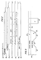
- a typical image signal output 49 from CCD 15 is there- shown.
- Portion 50 of the image signal 49 comprises the offset signal which is derived from the voltage bias Vc.
- Offset signal 50 has its origin in the non-image bearing phase gates of shift registers 18, 20, while introduction of the charges on cells 12 to the remaining phase gates of registers 18, 20 provides the signal 51 proportional to the intensity of the image viewed.
- offset signal 50 and image signal 51 are combined to provide the image signal 49.
- Areas 52, 52' exemplify a dark image area and a light image area respectively. Signals of this type may result for example, in the case where the original document comprises a series of dark lines with light-colored spaces therebetween.
- dark (D) and light (L) signals 54, 55 are dark (D) and light (L) signals 54, 55 respectively.
- signals 54, 55 result from generation of predetermined test or calibration signals in CCD 15.
- the image signals output by CCD 15 include an offset component.
- the offset component To restore the image signals to a true or absolute image signal level, i.e., one without an offset component, the offset component must be removed.
- the system gain be constant whatever the CCD used or the integration rate selected.
- Signal gain can vary from CCD to CCD, and with different integration rates.
- the image signals are modified by the application of a compensating gain factor derived from the instantaneous operating characteristics of the CCD in use.
- light signal (L) is derived from a suitable potential source, exemplified herein by battery 60.
- Output lead 61 of battery 60 is tapped by light signal input lead 65 between resistor pair 62, 63.
- battery 60 and resistor pair 62, 63 are chosen to provide the desired voltage level or potential for the light signal (L).
- Input lead 65 is coupled through a suitable switch such as FET 66 to auxiliary signal input gates 67, 68 of registers 18, 20.
- FET 66 is actuated periodically for a predetermined number of clock pulses, (e.g. 16) to input a series of light signals (L) to CCD registers 18, 20.
- Dark signal (D) is conveniently obtained by clocking registers 18, 20 a predetermined number of times (e.g. 16) beyond the last image signal. Inasmuch as no intervening exposure takes place, the signal produced in registers 18, 20 has a potential representative of the internal potential of CCD 15, i.e. the CCD offset signal.
- clock pulses 0g successively actuate FET 66 to input a series of light signals (L) the level of which is established by battery/resistor combination 60, 62, 63, to shift registers 18, 20.
- blocks 81, 82 of dark and light signals (D, L) are each 16 pulses wide.
- the stream of signals output by CCD 15, which are understood to be made up of a relatively large block of image signals (e.g. 1,728 pixels) followed by the relatively small (e.g. 16 pixels each) blocks 81, 82 of dark and light signals (D, L) are input to Analog-to-Digital (hereinafter A/D) converter 84 where the analog signals are converted to digital signals.
- A/D converter is a TRW Model TDC 10145 converter.
- Digital image signals from converter 84 are input to serial in/parallel out buffer 85.
- One suitable buffer is buffer Model No. 74S195 by TRW, Inc.
- buffer 85 need only be wide enough to handle the dark (D) and light (L) signals.
- buffer 85 may comprise a 32 bit buffer. It will be understood that the image signals, which precede the dark (D) and light (L) signals pass through buffer 85 and are discarded.
- Block 81 of dark signals (D) and block 82 of light signals (L) in buffer 85 are input to microprocessor MPU 86 through data bus 83.
- Microprocessor 86 which may comprise an Intel Model 8080 MPU by Intel Corp., averages the block of dark signals (D) in accordance with the following function: where,
- V(OFF) is the instantaneous average voltage offset signal (i.e. 50 in Figure 3)
- V D1 V D2 , ... V DN are the voltage levels of the individual dark signals that comprise block 81.
- the offset signal V(OFF) determined is output by MPU 86 via lead 87 to Digital-to-Analog (D/A herein) converter 88.
- MPU 86 averages the block of light signals (L) in accordance with the following function:
- VL (AVG) is the instantaneous average light signal
- V (OFF) and light signal VL (AVG) MPU 86 determines the instantaneous gain multiplicand K in accordance with the following relationship:
- VT represents the ideal voltage level output.
- Gain multiplicand K is output by MPU 86 via lead 89 to D/A converter 90.
- D/A converters 88, 90 may comprise Model DAC-08 converters made by Signets, Inc.
- D/A converters 88, 90 provide the analog equivalent of the offset signal V (OFF) and gain multiplicand K.
- the output of D/A converters 88, 90 are input to subtractor 92 and multiplier 94 respectively.
- One suitable subtractor is National Semi-Conductor Model 0032 Differential Amplifier while a suitable multiplier is Motorola Model 1595 Multiplier.
- Each succeeding line of signals output by CCD 15 is input via A/D converter 84 to buffer 85 where the dark (D) and light (L) level signals are processed by MPU 86 in the manner described heretofore. As fresh signals enter buffer 85, the previous blocks 81, 82 of dark (D) and light (L) level signals are discarded.
- Image signals in the output of CCD 15 are also placed on data output bus 100 which carries the image signals to subtractor 92 for processing.
- the offset signal V (OFF) as determined for the preceding line of image signals by MPU 86, is subtracted from the image signals thereby restoring the image signals to an absolute or substantially-absolute signal level.
- Image signals from subtractor 92 are input to multiplier 94 where the image signals are multiplied by the multiplicand factor K as determined by MPU 86 for the preceding line of image signals. This sets the image signal output level to assure a level commensurate with the ideal output level Vt in accommodation of the particular CCD being used and the existing integration time.
- the image signals are output by multiplier 94 for further processing and/or use.
- FET control gate 103 serves to limit the signal input to data bus 100 to image signals and exclude other signals, particularly dark and light signals (D, L).
- Clock pulse 07 actuates gate 103 in unison with the image signal output of CCD 15 to transfer image signals into bus 100. However, actuation of gate 103 is terminated following the last image signal to preclude passage of dark and light signals (D, L) into output bus 100.
- FETs 66, 103 may comprise Signetics Model No. SD5001 FETs.
- blocks 81, 82 of dark (D) and light (L) signals are generated with each line of image signals
- other relationships as for example, generating dark and light signals at the start of each page with calibration of CCD 15 once per page, may be envisioned.
- dark signals (D) may be derived from a source other than CCD bias source 25, that the potential levels of both the dark and light signals may comprise any suitable potential, and that the order in which dark and light signals are generated may be reversed.
- multiplier 94 is disclosed herein as being downstream of subtractor 92, the positions may be reversed. In that circumstance, suitable compensation must be made for the change in processing locations of the image signals as will be understood.
Landscapes
- Engineering & Computer Science (AREA)
- Multimedia (AREA)
- Signal Processing (AREA)
- Transforming Light Signals Into Electric Signals (AREA)
- Picture Signal Circuits (AREA)
- Facsimile Image Signal Circuits (AREA)
Applications Claiming Priority (2)
| Application Number | Priority Date | Filing Date | Title |
|---|---|---|---|
| US06/023,570 US4216503A (en) | 1979-03-26 | 1979-03-26 | Signal restoration and gain control for image viewing devices |
| US23570 | 1998-02-13 |
Publications (3)
| Publication Number | Publication Date |
|---|---|
| EP0016629A2 EP0016629A2 (en) | 1980-10-01 |
| EP0016629A3 EP0016629A3 (en) | 1980-10-15 |
| EP0016629B1 true EP0016629B1 (en) | 1984-03-14 |
Family
ID=21815913
Family Applications (1)
| Application Number | Title | Priority Date | Filing Date |
|---|---|---|---|
| EP80300824A Expired EP0016629B1 (en) | 1979-03-26 | 1980-03-19 | System and method for restoring image signal levels and setting signal gain for image-viewing devices |
Country Status (5)
| Country | Link |
|---|---|
| US (1) | US4216503A (cg-RX-API-DMAC7.html) |
| EP (1) | EP0016629B1 (cg-RX-API-DMAC7.html) |
| JP (1) | JPS55130276A (cg-RX-API-DMAC7.html) |
| CA (1) | CA1132244A (cg-RX-API-DMAC7.html) |
| DE (1) | DE3066908D1 (cg-RX-API-DMAC7.html) |
Families Citing this family (79)
| Publication number | Priority date | Publication date | Assignee | Title |
|---|---|---|---|---|
| JPS5650668A (en) * | 1979-09-29 | 1981-05-07 | Sharp Corp | Correcting system for reading output |
| US4351004A (en) * | 1980-01-31 | 1982-09-21 | Texas Instruments Incorporated | CCD Imager |
| US4345148A (en) * | 1980-10-06 | 1982-08-17 | Hughes Aircraft Company | Automatic responsivity control for a CCD imager |
| US4865427A (en) * | 1981-01-12 | 1989-09-12 | Massachusetts Institute Of Technology | Spatial light modulator |
| US4696533A (en) * | 1981-01-12 | 1987-09-29 | Massachusetts Institute Of Technology | Spatial light modulator |
| EP0060149B1 (en) * | 1981-01-14 | 1984-11-21 | Morton Nadler | Image scanning method and device |
| US4396938A (en) * | 1981-07-23 | 1983-08-02 | Rca Corporation | Controlled ram signal processor |
| US4408231A (en) * | 1981-07-31 | 1983-10-04 | International Business Machines Corporation | Method and apparatus for calibrating a linear array scanning system |
| US4635126A (en) * | 1981-12-18 | 1987-01-06 | Canon Kabushiki Kaisha | Image pick-up system |
| US4554460A (en) * | 1982-07-02 | 1985-11-19 | Kollmorgen Technologies Corp. | Photodetector automatic adaptive sensitivity system |
| US4525741A (en) * | 1982-11-03 | 1985-06-25 | Ncr Corporation | Self-adjusting video camera |
| DE3408108A1 (de) * | 1983-03-06 | 1984-09-06 | Canon K.K., Tokio/Tokyo | Bildaufbereitungseinrichtung |
| US4745466A (en) * | 1983-03-06 | 1988-05-17 | Canon Kabushiki Kaisha | Digital color image processing apparatus with color masking processing unit addressed by a plurality of multi-bit color component signals using various combinations of the bits of the signals |
| US4578711A (en) * | 1983-12-28 | 1986-03-25 | International Business Machines (Ibm) | Video data signal digitization and correction system |
| US4590505A (en) * | 1984-01-10 | 1986-05-20 | The United States Of America As Represented By The Secretary Of The Air Force | Three dimensional optical receiver having programmable gain sensor stages |
| US4584610A (en) * | 1984-02-16 | 1986-04-22 | Olympus Optical Co., Ltd. | Electronic photographing apparatus |
| JPS60189372A (ja) * | 1984-03-08 | 1985-09-26 | Dainippon Screen Mfg Co Ltd | 画像入力装置 |
| US4555732A (en) * | 1984-03-22 | 1985-11-26 | Xerox Corporation | Image sensor correction system |
| US4636980A (en) * | 1984-07-25 | 1987-01-13 | Westinghouse Electric Corp. | Three dimensional optical receiver having programmable gain control |
| JPS6153868A (ja) * | 1984-08-24 | 1986-03-17 | Dainippon Screen Mfg Co Ltd | 画像走査信号処理におけるキャリブレーション装置 |
| GB8506050D0 (en) * | 1985-03-08 | 1985-04-11 | Crosfield Electronics Ltd | Operating ccd arrays |
| DE3671689D1 (de) * | 1985-09-04 | 1990-07-05 | Philips Nv | Kamera zur aufzeichnung von fernseh- und kinobildern oder fotografien. |
| US5737016A (en) * | 1985-11-15 | 1998-04-07 | Canon Kabushiki Kaisha | Solid state image pickup apparatus for reducing noise |
| US4914519A (en) * | 1986-09-19 | 1990-04-03 | Canon Kabushiki Kaisha | Apparatus for eliminating noise in a solid-state image pickup device |
| JPH084127B2 (ja) * | 1986-09-30 | 1996-01-17 | キヤノン株式会社 | 光電変換装置 |
| US5771070A (en) * | 1985-11-15 | 1998-06-23 | Canon Kabushiki Kaisha | Solid state image pickup apparatus removing noise from the photoelectric converted signal |
| GB8606200D0 (en) * | 1986-03-13 | 1986-04-16 | Crosfield Electronics Ltd | Operating radiation sensors |
| JPS62293384A (ja) * | 1986-06-11 | 1987-12-19 | Toshiba Corp | 画像入力装置 |
| US4991127A (en) * | 1986-08-28 | 1991-02-05 | Hughes Aircraft Company | Offset and gain correction system for image data processing |
| US4862286A (en) * | 1986-11-14 | 1989-08-29 | Canon Kabushiki Kaisha | Image reading apparatus which adjusts image signals to improve signal balance |
| US5121230A (en) * | 1987-01-19 | 1992-06-09 | Canon Kabushiki Kaisha | Image reading apparatus having adjusting circuits for matching the level of and compensating for fluctuation among a plurality of sensing elements |
| DE3723508C1 (de) * | 1987-07-16 | 1988-11-03 | Fraunhofer Ges Forschung | Schaltungsanordnung zur Grauwertkorrektur von Videosignalen |
| US4920428A (en) * | 1988-07-08 | 1990-04-24 | Xerox Corporation | Offset, gain and bad pixel correction in electronic scanning arrays |
| US4903144A (en) * | 1988-10-27 | 1990-02-20 | Eastman Kodak Company | Automatic D.C. offset control for image scanners |
| US5267053A (en) * | 1988-10-27 | 1993-11-30 | Eastman Kodak Company | Automatic reference control for image scanners |
| JPH02164184A (ja) * | 1988-12-19 | 1990-06-25 | Toshiba Corp | X線診断装置 |
| JPH0693768B2 (ja) * | 1988-12-27 | 1994-11-16 | 日本電気株式会社 | 撮像信号処理装置 |
| US5008739A (en) * | 1989-02-13 | 1991-04-16 | Eastman Kodak Company | Real-time digital processor for producing full resolution color signals from a multi-color image sensor |
| US4979042A (en) * | 1989-05-30 | 1990-12-18 | Eastman Kodak Company | Apparatus for correcting shading effects in video images |
| US4970598A (en) * | 1989-05-30 | 1990-11-13 | Eastman Kodak Company | Method for correcting shading effects in video images |
| JP2787710B2 (ja) * | 1989-06-07 | 1998-08-20 | 株式会社ニコン | 光電変換装置の信号補正装置 |
| US4984085A (en) * | 1989-08-03 | 1991-01-08 | Allen-Bradley Company, Inc. | Image processor with dark current compensation |
| US5065443A (en) * | 1989-12-04 | 1991-11-12 | Allen-Bradley Company, Inc. | Image processor with illumination variation compensation |
| US5214518A (en) * | 1989-12-22 | 1993-05-25 | Fuji Xerox Co., Ltd. | Multiple value image input equipment |
| DE69126895T2 (de) * | 1990-01-25 | 1997-11-20 | Hewlett Packard Co | Verfahren und Vorrichtung zur Ausstattung eines Dokumentenlesers mit Sensorkompensation |
| DE69116905T2 (de) * | 1990-03-13 | 1996-06-13 | Sony Corp., Tokio/Tokyo | Schattierungseffektenkorrekturvorrichtung |
| US5086343A (en) * | 1990-05-11 | 1992-02-04 | Eastman Kodak Company | Method and apparatus for compensating for sensitivity variations in the output of a solid state image sensor |
| US5047863A (en) * | 1990-05-24 | 1991-09-10 | Polaroid Corporation | Defect correction apparatus for solid state imaging devices including inoperative pixel detection |
| US5047861A (en) * | 1990-07-31 | 1991-09-10 | Eastman Kodak Company | Method and apparatus for pixel non-uniformity correction |
| EP0553286A4 (en) * | 1990-10-15 | 1993-11-03 | The Gerber Scientific Instrument Company | A large area digital scanner |
| US5204761A (en) * | 1991-03-18 | 1993-04-20 | Xerox Corporation | Pixel by pixel offset and gain correction in analog data from scanning arrays |
| JPH04365264A (ja) * | 1991-06-12 | 1992-12-17 | Ricoh Co Ltd | 原稿読取装置 |
| US5157500A (en) * | 1991-09-30 | 1992-10-20 | Xerox Corporation | Amplifier-return-driven CCD offset control for scanning arrays |
| US5153421A (en) * | 1991-11-04 | 1992-10-06 | Xerox Corporation | Architecture for analog and digital image sensor arrays |
| JP2725508B2 (ja) * | 1991-12-30 | 1998-03-11 | 日本電気株式会社 | 多素子光センサ装置 |
| US5361140A (en) * | 1992-02-18 | 1994-11-01 | Neopath, Inc. | Method and apparatus for dynamic correction of microscopic image signals |
| DE69318885T2 (de) * | 1992-05-04 | 1999-01-21 | Agfa-Gevaert N.V., Mortsel | Automatische Verschiebung und Verstärkungssteuerung für einen Dokumentenabtaster |
| DE69316569T2 (de) * | 1992-12-23 | 1998-08-20 | Eastman Kodak Co | Automatischer Abgleich der Kanalverstärkung und -abweichung für Videokameras mit Multikanalsensoren |
| JP3297946B2 (ja) * | 1993-03-23 | 2002-07-02 | ソニー株式会社 | 電荷転送装置 |
| US5519441A (en) * | 1993-07-01 | 1996-05-21 | Xerox Corporation | Apparatus and method for correcting offset and gain drift present during communication of data |
| JP3318905B2 (ja) * | 1993-12-03 | 2002-08-26 | ソニー株式会社 | 電荷転送装置 |
| JP3525500B2 (ja) * | 1994-07-26 | 2004-05-10 | ミノルタ株式会社 | 固体撮像装置 |
| US6038038A (en) * | 1994-08-24 | 2000-03-14 | Xerox Corporation | Method for determining offset and gain correction for a light sensitive sensor |
| US5563723A (en) * | 1994-08-31 | 1996-10-08 | Eastman Kodak Company | Method of calibration of image scanner signal processing circuits |
| US5621217A (en) * | 1995-09-28 | 1997-04-15 | Xerox Corporation | Apparatus and method for calibrating a digital scanner |
| FR2743144B1 (fr) * | 1995-12-28 | 1998-01-30 | Sagem | Procede de determination d'une energie lumineuse mesuree par un capteur |
| JP3774499B2 (ja) | 1996-01-24 | 2006-05-17 | キヤノン株式会社 | 光電変換装置 |
| DE19605938B4 (de) * | 1996-02-17 | 2004-09-16 | Fachhochschule Wiesbaden | Bildabtaster |
| US7173656B1 (en) * | 1997-12-03 | 2007-02-06 | Intel Corporation | Method and apparatus for processing digital pixel output signals |
| US6327047B1 (en) * | 1999-01-22 | 2001-12-04 | Electronics For Imaging, Inc. | Automatic scanner calibration |
| US6900448B1 (en) * | 2000-07-31 | 2005-05-31 | Hewlett-Packard Development Company L.P. | Method and system for dynamic scanner calibration |
| US7149002B2 (en) * | 2000-12-21 | 2006-12-12 | Hewlett-Packard Development Company, L.P. | Scanner including calibration target |
| US7050098B2 (en) * | 2001-03-29 | 2006-05-23 | Canon Kabushiki Kaisha | Signal processing apparatus and method, and image sensing apparatus having a plurality of image sensing regions per image frame |
| US7333423B2 (en) * | 2004-03-31 | 2008-02-19 | Intel Corporation | Transceiver with calibrated I and Q paths and methods for deconvolved calibration |
| US8076925B2 (en) * | 2009-10-28 | 2011-12-13 | Optisense Network, Inc. | Optical sensor assembly for installation on a current carrying cable |
| US9134344B2 (en) | 2009-10-28 | 2015-09-15 | Gridview Optical Solutions, Llc. | Optical sensor assembly for installation on a current carrying cable |
| US8395372B2 (en) * | 2009-10-28 | 2013-03-12 | Optisense Network, Llc | Method for measuring current in an electric power distribution system |
| US9535097B2 (en) | 2012-07-19 | 2017-01-03 | Gridview Optical Solutions, Llc. | Electro-optic current sensor with high dynamic range and accuracy |
| US9146358B2 (en) | 2013-07-16 | 2015-09-29 | Gridview Optical Solutions, Llc | Collimator holder for electro-optical sensor |
Family Cites Families (8)
| Publication number | Priority date | Publication date | Assignee | Title |
|---|---|---|---|---|
| GB1391452A (en) * | 1971-04-21 | 1975-04-23 | Image Analysing Computers Ltd | Method and circuit arrangement for amplitude correction of a video signal obtained by line scanning |
| US3962681A (en) * | 1972-06-19 | 1976-06-08 | Recognition Equipment Incorporated | Page width optical character processing method and system |
| US3800079A (en) * | 1972-12-18 | 1974-03-26 | Ibm | Compensation for a scanning system |
| US3800078A (en) * | 1972-12-18 | 1974-03-26 | Ibm | Digitally compensated scanning system |
| GB1526801A (en) * | 1976-01-08 | 1978-10-04 | British Broadcasting Corp | Compensating interference from solid state image sensing devices |
| US4065788A (en) * | 1976-02-09 | 1977-12-27 | Mcdonnell Douglas Corporation | Realtime image processor |
| US4074320A (en) * | 1976-12-13 | 1978-02-14 | Bell Telephone Laboratories, Incorporated | High quality light emitting diode array imaging system |
| US4129853A (en) * | 1977-09-26 | 1978-12-12 | International Business Machines Corporation | Method and apparatus for producing compensated signals for individual light sensors arranged in a predetermined relation |
-
1979
- 1979-03-26 US US06/023,570 patent/US4216503A/en not_active Expired - Lifetime
-
1980
- 1980-01-14 CA CA343,642A patent/CA1132244A/en not_active Expired
- 1980-03-04 JP JP2725780A patent/JPS55130276A/ja active Granted
- 1980-03-19 EP EP80300824A patent/EP0016629B1/en not_active Expired
- 1980-03-19 DE DE8080300824T patent/DE3066908D1/de not_active Expired
Also Published As
| Publication number | Publication date |
|---|---|
| US4216503A (en) | 1980-08-05 |
| DE3066908D1 (en) | 1984-04-19 |
| EP0016629A2 (en) | 1980-10-01 |
| JPS6342906B2 (cg-RX-API-DMAC7.html) | 1988-08-26 |
| EP0016629A3 (en) | 1980-10-15 |
| JPS55130276A (en) | 1980-10-08 |
| CA1132244A (en) | 1982-09-21 |
Similar Documents
| Publication | Publication Date | Title |
|---|---|---|
| EP0016629B1 (en) | System and method for restoring image signal levels and setting signal gain for image-viewing devices | |
| US5153421A (en) | Architecture for analog and digital image sensor arrays | |
| EP1968307B1 (en) | Image sensing apparatus and image sensing system | |
| JPS60214173A (ja) | イメージセンサ用オフセット補正装置 | |
| US5654755A (en) | System for determining a video offset from dark photosensors in an image sensor array | |
| US4620236A (en) | Image picture reading device | |
| EP0185498B1 (en) | Imaging sensing and processing apparatus and method | |
| EP0292253B1 (en) | Contact-type image scanner | |
| JPH10136273A (ja) | Ccdセンサのs/n比改善方法 | |
| EP0397669B1 (en) | Input scanner | |
| EP0984625A1 (en) | Photoelectric transducer and solid-state image pickup device | |
| EP0185487B1 (en) | Electronic image scanner with colour matrix image enhancement | |
| JPS59106149A (ja) | Ccdイメ−ジヤ | |
| US6201617B1 (en) | Image sensing device | |
| JPH09298647A (ja) | リニアイメージセンサのオフセットレベル補正方法およびその装置 | |
| JP2004112645A (ja) | 画像読取装置 | |
| US6853402B2 (en) | Combined multiplexing and offset correction for an image sensor array | |
| JP4192111B2 (ja) | 画像入力装置 | |
| US4754153A (en) | Operating radiation sensors to avoid transfer loss | |
| US4864407A (en) | Pick up device having pick up elements arranged in a predetermined pattern and smear component reduction varying independence upon the position of a pick up element in the pattern | |
| JPH023232B2 (cg-RX-API-DMAC7.html) | ||
| US4675744A (en) | Scanning system | |
| EP0659014B1 (en) | Solid state image sensing device and charge transfer method thereof | |
| JP3157526B2 (ja) | 電荷結合素子のmtf補正方法及び画像読み取り装置 | |
| US20030147111A1 (en) | Arrangement and method for correcting different transfer characteristic curves for segmented image sensors (CCDs) |
Legal Events
| Date | Code | Title | Description |
|---|---|---|---|
| PUAI | Public reference made under article 153(3) epc to a published international application that has entered the european phase |
Free format text: ORIGINAL CODE: 0009012 |
|
| PUAL | Search report despatched |
Free format text: ORIGINAL CODE: 0009013 |
|
| AK | Designated contracting states |
Designated state(s): DE FR GB NL |
|
| AK | Designated contracting states |
Designated state(s): DE FR GB NL |
|
| 17P | Request for examination filed |
Effective date: 19810119 |
|
| GRAA | (expected) grant |
Free format text: ORIGINAL CODE: 0009210 |
|
| AK | Designated contracting states |
Designated state(s): DE FR GB NL |
|
| REF | Corresponds to: |
Ref document number: 3066908 Country of ref document: DE Date of ref document: 19840419 |
|
| ET | Fr: translation filed | ||
| PGFP | Annual fee paid to national office [announced via postgrant information from national office to epo] |
Ref country code: DE Payment date: 19840427 Year of fee payment: 5 |
|
| PLBE | No opposition filed within time limit |
Free format text: ORIGINAL CODE: 0009261 |
|
| STAA | Information on the status of an ep patent application or granted ep patent |
Free format text: STATUS: NO OPPOSITION FILED WITHIN TIME LIMIT |
|
| 26N | No opposition filed | ||
| PG25 | Lapsed in a contracting state [announced via postgrant information from national office to epo] |
Ref country code: GB Effective date: 19890319 |
|
| GBPC | Gb: european patent ceased through non-payment of renewal fee | ||
| PG25 | Lapsed in a contracting state [announced via postgrant information from national office to epo] |
Ref country code: DE Effective date: 19891201 |
|
| PGFP | Annual fee paid to national office [announced via postgrant information from national office to epo] |
Ref country code: FR Payment date: 19970313 Year of fee payment: 18 |
|
| PGFP | Annual fee paid to national office [announced via postgrant information from national office to epo] |
Ref country code: NL Payment date: 19970331 Year of fee payment: 18 |
|
| PG25 | Lapsed in a contracting state [announced via postgrant information from national office to epo] |
Ref country code: FR Free format text: THE PATENT HAS BEEN ANNULLED BY A DECISION OF A NATIONAL AUTHORITY Effective date: 19980331 |
|
| PG25 | Lapsed in a contracting state [announced via postgrant information from national office to epo] |
Ref country code: NL Free format text: LAPSE BECAUSE OF NON-PAYMENT OF DUE FEES Effective date: 19981001 |
|
| NLV4 | Nl: lapsed or anulled due to non-payment of the annual fee |
Effective date: 19981001 |
|
| REG | Reference to a national code |
Ref country code: FR Ref legal event code: ST |