EP0009862B1 - Programmable mode of operation select by reset and data processor using this select - Google Patents
Programmable mode of operation select by reset and data processor using this select Download PDFInfo
- Publication number
- EP0009862B1 EP0009862B1 EP19790301475 EP79301475A EP0009862B1 EP 0009862 B1 EP0009862 B1 EP 0009862B1 EP 19790301475 EP19790301475 EP 19790301475 EP 79301475 A EP79301475 A EP 79301475A EP 0009862 B1 EP0009862 B1 EP 0009862B1
- Authority
- EP
- European Patent Office
- Prior art keywords
- coupled
- terminal
- mosfet
- circuitry
- signal
- Prior art date
- Legal status (The legal status is an assumption and is not a legal conclusion. Google has not performed a legal analysis and makes no representation as to the accuracy of the status listed.)
- Expired
Links
Images


Classifications
-
- G—PHYSICS
- G06—COMPUTING OR CALCULATING; COUNTING
- G06F—ELECTRIC DIGITAL DATA PROCESSING
- G06F1/00—Details not covered by groups G06F3/00 - G06F13/00 and G06F21/00
- G06F1/24—Resetting means
Definitions
- This invention relates generally to a data processor and more particularly to circuitry for selecting the mode of operation for a data processor.
- One prior art approach for providing various configurations of the input-output circuitry for a data processor is to provide a plurality of mask options which vary the integrated circuit metal interconnections during processing such that a particular metal mask is used to provide an integrated circuit data processor of the desired configuration.
- this approach results in higher costs for processing, testing, and inventory control since each mask option results in a unique integrated circuit.
- Another prior art approach is to make the configuration of the processor device software programmable such that instructions are stored in a program memory which must be executed by the processor to achieve the desired configuration of the input-output circuitry for the data processor device.
- this approach increases the number of storage locations required for the program memory.
- a third prior art approach is to hardware-program the mode of operation by providing separate program selection inputs to the data processor for configuring the input-output circuit. This approach is also costly in that additional package pins are required for the integrated circuit device in order to determine the mode of operation.
- a data processor of the type which includes storage elements for storing digital information, the data processor including reset circuitry for receiving a reset signal, the reset circuitry being responsive to the reset signal for causing the storage elements to store predetermined digital information and for initiating execution of instructions stored in a memory, the data processor also including input-output circuitry having at least one terminal for transmitting at least one digital signal, the at least one digital signal having first and second logic states characterized by:
- a circuit adapted for implementation within an integrated circuit data processor and suitable for selecting a mode of operation for the data processor, including
- a first terminal for receiving a reset signal, the reset signal having a voltage ranging between a first and a second voltage level
- reset circuitry coupled to the first terminal and responsive to the reset signal for generating a control signal when the reset signal voltage reaches a first predetermined voltage, the control signal being operative to initialize the data processor; characterized by:
- a circuit adapted for implementation within an integrated circuit data processor, the circuit including a reset terminal for receiving a reset signal, circuitry responsive to the reset signal for causing initialization of the data processor, one or more input-output terminals which are generally used to transmit digital information to and from the data processor but receive one or more mode selection signals when the data processor is being reset, a level detector responsive to the reset signal which generates an output signal when the reset voltage reaches a predetermined level, and storage circuitry adapted for storing the one or more mode selection signals when the level detector generates the output signal.
- level shifting circuitry which shifts the voltage level of the mode selection signal such that the mode selection signal may be generated by either connecting a diode between the input-output terminal and the reset terminal for causing a mode selection signal to assume a first logic state or omitting the diode and causing the mode selection signal to assume the second logic state.
- Fig. 1 is a circuit schematic of circuitry associated with an input-output terminal of a data processor including conventional input- output circuitry within dashed block 2 and mode selection circuitry within dashed block 4.
- Input- output terminal 6 is coupled to node 8
- node 8 is coupled to node 10 by resistor 12.
- MOSFET device 14 has its drain coupled to node 10 while the gate and source are coupled to ground potential. Since the operation of MOSFETs (metal-oxide-semiconductor field- effect transistors) is well-known by those skilled in the art, it will not be described in further detail herein. For an explanation of the operation of MOSFETs, see “Physics and Technology of Semiconductor Devices" by A. S.
- MOSFET device 14 serves as an input protection device so as to prevent the potential at node 10 from becoming so negative as to cause damage to other devices within the circuit.
- Node 10 is coupled to the input of inverter 16 which has an output coupled to one terminal of MOSFET device 18.
- the gate terminal of MOSFET 18 is coupled to control signal R102 such that MOSFET 18 is conductive when control signal R102 is at a high level.
- a third terminal of MOSFET 18 is coupled to the input of inverter 20.
- the output of inverter 20 is coupled to PDBO conductor 22 by MOSFET 24.
- the gate terminal of MOSFET 24 is coupled to conductor 26 which conducts a control signal R102 such that MOSFET 24 is conductive when R102 is at a high level.
- Conductor 22 corresponds to the least significant bit of a data bus within the data processor in the preferred embodiment of the invention.
- PDBO conductor 22 may be used to transfer digital information between input/output circuitry block 2 and working registers (not shown) within the data processor.
- control signal R102 is initially at a high level while control signal R102 is initially at a low level.
- the signal received by input/output pin 6 is coupled to the input of inverter 16 by resistor 12, and the inverted output signal is coupled to the input of inverter 20 by MOSFET 18.
- control signal R102 switches to a low level while control signal R102 switches to a high level such that MOSFET 18 turns off while MOSFET 24 becomes conductive.
- the inverted signal initially coupled to the input of inverter 20 by MOSFET 18 is dynamically stored on the input of inverter 20 after MOSFET 18 is turned off.
- the output of inverter 20 is then coupled by MOSFET 24 to PDBO conductor 22 in order to complete the transfer of the digital information to the internal data bus.
- PDBO conductor 22 is also coupled to the input of inverter 28 by MOSFET 30.
- the gate terminal of MOSFET 30 is coupled to conductor 32 which conducts control signals WP2 such that MOSFET 30 is conductive when WP2 is at a high level.
- the output of inverter 28 is coupled to node 34 by MOSFET 36 and is also coupled to node 38 by MOSFET 40.
- the gate terminal of MOSFET 36 is coupled to conductor 42 which conducts control signal W102 such that MOSFET 36 is conductive when W102 is at a high level.
- the gate terminal of MOSFET 40 is coupled to conductor 44 which conducts control signal DDR2 such that MOSFET 40 is conductive when DDR2 is at a high level.
- Node 34 is coupled to the input of inverter 46 which has an output coupled to the input of inverter 48 and to a first input of NOR gate 50.
- the output of inverter 48 is coupled to node 34 by MOSFET 52 which has its gate terminal coupled to positive supply voltage V DD .
- Inverter 46, inverter 48, and MOSFET 52 form a feedback latching circuit.
- Node 38 is coupled to a first input of NOR gate 54 while the second input of gate 54 is coupled to conductor 56 which conducts control signal RESET.
- the output of gate 54 is coupled to the input of inverter 58 which has an output coupled to node 60.
- Node 60 is coupled to node 38 by MOSFET 62 which has a gate terminal coupled to the positive supply voltage V DD .
- NOR gate 54, inverter 58, and MOSFET 62 form a feedback latching circuit which may be a portion of a data direction register as will be explained later.
- Node 60 is coupled to the second input of gate 50 and is also coupled to a first input of NOR gate 64.
- the output of gate 50 is coupled to the second input of gate 64 and to the gate terminal of MOSFET 66.
- MOSFET 66 The source of MOSFET 66 is coupled to ground potential while the drain of MOSFET 66 is coupled to node 8.
- the output of gate 64 is coupled to the gate terminal of enhancement mode MOSFET 68 which has its drain terminal coupled to the positive supply voltage V DD and its source coupled to node 8.
- a depletion mode MOSFET 70 has a drain terminal coupled to the positive supply voltage V DD while its gate and source terminals are coupled to node 8.
- MOSFET 66 and MOSFET 68 are turned off such that node 8 is allowed to appear as a high impedance.
- node 60 is at a high level or logic "1"
- gate 64 and gate 50 both output a low level such that MOSFET devices 66 and 68 are cut off.
- the RESET control signal coupled to conductor 56 assumes a logic 1" " level which causes the data direction register latch formed by gates 54, 58 and MOSFET 62 to store a logic "1" on node 60.
- the data direction register must be caused to store a logic "0" on node 60. This may be accomplished by providing a logic "1" level on conductor 22 and enabling MOSFET 30 and MOSFET 40 by causing control signal WP2 and control signal DDR2 to be at a high level.
- the logic state of input/output pin 6 is determined by the logic state stored by the latch formed by gates 46, 48 and MOSFET 52. The logic state on PDBO conductor 22 will be copied into the latch by enabling MOSFETs 30 and 36 by forcing control signal WP2 and W102 to a high level.
- the decoder circuitry for generating the various control signals is conventional and will not be described herein.
- Node 10 is also coupled to enhancement mode MOSFET 72 within dashed block 4.
- the drain of MOSFET 72 is coupled to the positive supply voltage V DD and the source is coupled to node 74.
- Node 74 is coupled to the input of inverter 76 and is also coupled to the drain of MOSFET 78.
- the source of MOSFET 78 is coupled to ground potential while the gate terminal is coupled to conductor 80 which conducts a bias voltage which will be later discussed with reference to Fig. 2.
- MOSFET 72 acts as a level shifter or source-follower while MOSFET 78 acts as a current source.
- inverter 76 is coupled to the input of inverter 82.
- the output of inverter 82 is coupled to node 84 by MOSFET 86.
- the gate terminal of MOSFET 86 is coupled to conductor 88 which conducts a control signal V MODL which will be later discussed with reference to Fig. 2.
- Node 84 is coupled to the input of inverter 90, and the output of inverter 90 is coupled to the input of inverter 92.
- the output of inverter 92 is coupled to node 94, and node 94 is coupled to node 84 by feedback MOSFET 96.
- MOSFET 96 The gate terminal of MOSFET 96 is coupled to the positive supply voltage V DD such that inverter 90, inverter 92, and MOSFET 96 form a feedback latching circuit.
- the logic state stored by the latching circuit can be initialized by causing control signal V MODL to be a high level such that MOSFET 86 is made conductive. At such time, the voltage at input/output pin 6 will determine the logic state stored by the latching circuit.
- the mode programming latch register formed by inverter 90, inverter 92 and MOSFET 96 is initialized when the data processor is reset. Shown in Fig. 1 is RESET input pin 98 and a diode 100 having its anode coupled to input/output pin 6 and its cathode coupled to RESET pin 98. Diode 100 would be included if it is desired to store a logic "0" in the mode programming latch register. In this event, when RESET pin 98 goes to a low level in order to reset the data processor, then diode 100 pulls pin 6 to within .7 volt of a low logic level.
- Level shifting MOSFET 72 translates the voltage on pin 6 by one MOSFET threshold drop to a more negative voltage such that the input of inverter 76 recognizes the voltage on pin 6 as a low level. If it is desired for the mode programming latch register to latch a logic "1" level, then diode 100 is omitted and depletion mode pullup MOSFET 70 establishes a high level on pin 6.
- the output of mode programming latch register node 94 is coupled to decoder circuitry for controlling the configuration of the data processor circuit. Also, the output of mode programming latch register node 94 is coupled to PDB5 conductor 102 by MOSFET 104 such that the status of the mode programming latch register can be accessed by the internal data bus of the data processor. The gate terminal of MOSFET 104 is coupled to conductor 26 such that MOSFET 104 is conductive when control signal R102 is at a high level.
- circuitry for generating a reset signal to initialize the data processor is shown within block 106.
- circuitry is shown for generating the control signal V MODL already referred to within Fig. 1.
- bias circuitry is shown for generating various bias points.
- RESET input pin 98 is coupled to node 112 by input resistor 114.
- Node 112 is coupled to the gate and source terminals of enhancement mode MOSFET 116 which has its drain terminal coupled to the positive supply voltage V DD .
- Node 112 is also coupled to the drain terminal of enhancement mode MOSFET 118 which has its gate and source terminals coupled to ground potential.
- MOSFETs 116 and. 118 are input protection devices and serve to limit the magnitude of the voltage on node 112 so as to protect other MOSFET devices coupled to this node.
- Node 112 is coupled to the gate terminal of MOSFET 120 which has its drain terminal coupled to node 122 and its source terminal coupled to node 124.
- Node 124 is coupled to the source terminal of depletion mode MOSFET 126 and to the drain terminal of MOSFET 128.
- MOSFET 128 has its gate terminal coupled to the positive supply voltage V DD and its source terminal coupled to ground potential such that MOSFET 128 functions as a current source.
- MOSFET 126 has its drain coupled to the positive supply voltage V DD and its gate terminal coupled to node 122.
- Node 122 is also coupled to the source and gate terminals of depletion mode MOSFET 130 which has its drain terminal coupled to the source terminal of enhancement mode MOSFET 132.
- MOSFET 132 The gate and drain terminals of MOSFET 132 are coupled to the positive supply voltage V DD .
- MOSFET 120 and 126 form a differential amplifier connected as a Schmidt trigger circuit.
- the voltage on the gate terminal of MOSFET 126 varies as the drain current from MOSFET 128 is switched between MOSFET 120 and MOSFET 126 so as to provide hysteresis.
- Node 122 is also coupled to the input of inverter 134, which has an output coupled to the input of inverter 136.
- the output of inverter 136 is coupled to terminal 137 by conductor 138.
- Terminal 137 may be coupled to synchronization circuitry (not shown) such that the asynchronous reset signal provided by terminal 137 may by sychronized with clock signals generated within the data processor to provide a synchronized RESET signal.
- the synchronized RESET signal may then be used to clear the registers within the data processor and to initiate execution of instruction stored in the program memory.
- the synchronized RESET signal may also be used to initialize the data direction register which controls input/output circuitry.
- Node 112 is also coupled to the gate terminal of MOSFET 140 within dashed block 108.
- the source terminal of MOSFET 140 is coupled to the source terminal of MOSFET 142 and to the drain terminal of MOSFET 144.
- the gate terminal of MOSFET 144 is coupled to conductor 80 which provides a first bias voltage VRBIAS.
- the source of MOSFET 144 is coupled to ground potential such that MOSFET 144 functions as a current source.
- the gate terminal of MOSFET 142 is coupled to conductor 146 which provides a second bias voltage.
- MOSFET 140 and MOSFET 142 function as a differential comparator circuit for comparing the voltage on node 112 to the bias voltage provided by conductor 146.
- MOSFET 140 is coupled to the source terminal of enhancement mode MOSFET 148 which has its gate and drain terminals coupled to the positive supply voltage V DD such that MOSFET 148 functions as a load impedance.
- the drain of MOSFET 140 is also coupled to the gate terminal of MOSFET 150.
- the drain terminal of MOSFET 142 is coupled to the source terminal of enhancement mode MOSFET 152 which has its gate and drain terminals coupled to the positive supply voltage V DD .
- the drain terminal of MOSFET 142 is also coupled to the gate terminal of MOSFET 154.
- MOSFET 154 has its drain terminal coupled to the positive supply voltage V DD , and its source terminal is coupled to the gate and drain terminals of MOSFET 156 as well as to the gate terminal of MOSFET 158.
- MOSFET 156 and the source terminal of MOSFET 158 are coupled to ground potential such that MOSFET 156 and MOSFET 158 form a current mirror arrangement.
- the drain terminal of MOSFET 158 is coupled to the source of MOSFET 150 and to the input of inverter 160.
- the drain of MOSFET 150 is coupled to the positive supply voltage V DD .
- the output of inverter 160 is coupled to the input of inverter 162, and the output of inverter 162 is coupled to conductor 88 for providing the control signal V MODL .
- MOSFET 164 has its gate and drain terminals coupled to the positive supply voltage V oo , while the source terminal of MOSFET 164 is coupled to the gate and drain terminals of MOSFET 166.
- the source of MOSFET 166 is coupled to conductor 80 for providing bias voltage V RBIAS .
- the source of MOSFET 166 is also coupled to the gate and drain terminals of MOSFET 168, and the source of MOSFET 168 is coupled to conductor 146 for providing a second bias voltage.
- the source of MOSFET 168 is also coupled to the gate and drain terminals of MOSFET 170 and the source of MOSFET 170 is coupled to ground potential.
- the comparator circuit or level detector shown within dashed block 108 functions in the following manner. If the voltage on RESET pin 98 is less than the bias voltage provided by conductor 146, then MOSFET 140 will be non-conductive, while the drain terminal of MOSFET 142 will conduct the current provided by MOSFET 144. The current conducted by MOSFET 142 pulls the source of MOSFET 152 to a low level, thereby cutting off MOSFET 154. The source terminal of MOSFET 148 pulls the gate of MOSFET 150 to a high level, thereby allowing MOSFET 150 to conduct. Since MOSFET 154 is non-conductive, no bias current is provided to MOSFET 156, and MOSFET 158 is non-conductive.
- the input to inverter 160 is a high level.
- MOSFET 140 is conductive and MOSFET 142 is non-conductive.
- MOSFET 150 is pulled down to a low level, while the gate terminal of MOSFET 154 is pulled up to a high level.
- MOSFET 156 is made conductive by the current supplied by MOSFET 154, and MOSFET 158 is made conductive by the gate to source voltage developed across MOSFET 156.
- the input to inverter 160 is now a low level.
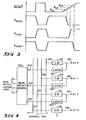
- timing waveforms are shown for the voltage at the RESET input pin as well as voltages for other points in the circuit.
- Two cases are shown for the RESET input voltage.
- an input pulse with relatively fast rising and falling edges is shown which may correspond to the voltage produced by the output of a TTL (transistor-transistor logic) logic circuit.
- a slowly rising input voltage is shown which may correspond to the voltage produced on the RESET input pin when this input pin is coupled to the positive supply voltage V oo by an appropriate RC network.
- Such a connection might be desired to automatically reset the data processor whenever the data processor is initially coupled to the power supply voltage.
- the Schmidt trigger circuit shown within dashed block 106 will switch when the input voltage reaches a predetermined voltage.
- this predetermined voltage (V RR ) is roughly 3.3 volts in the preferred embodiment.
- the waveform labeled V RESET in Fig. 3 shows the voltage provided by terminal 137 in the Schmidt trigger circuitry of Fig. 2, and it will be noted that this voltage switches to a low level when the RESET input voltage reaches the V RR .
- the input/output circuitry associated with pin 6 (Fig. 1) is forced to be in the input mode. However, once the RESET input voltage surpasses V RR ,.
- the software instructions executed by the data processor may change the input/output circuitry associated with pin 6 to select the output mode of operation.
- the level detector circuit within dashed block 108 of Fig. 2 functions to latch the mode programming latch register prior to the time that the data processor reset signal V RESET . switches to a low level.
- the waveform labelled V MODL shows the voltage produced on conductor 88 by the level detector circuitry within dashed block 108 in Fig. 2.
- the bias voltage provided by conductor 146 is selected such that V MODL switches to a low level when the RESET input voltage reaches voltage V RL which, in the preferred embodiment, is roughly 1 volt.
- V MOOL switches to a low level
- the input to the mode programming latch register is disabled such that the mode of operation is selected before the restart software routine can alter input/output pin 6 to assume the output mode of operation.
- one method of programming input/output pin 6 to be a low level during mode selection is to connect a diode from pin 6 to the RESET input pin 98.
- This' feature imposes the constraint that the mode programming latch register must latch the low logic level on pin 6 before the RESET input voltage rises sufficiently positive to make the voltage on pin 6 approach a high logic level.
- the waveform labeled V PGM in Fig. 3 corresponds to the voltage output by inverter 82 in Fig. 1 assuming that a diode has been connected as suggested, in this case, the level shifting circuitry formed by MOSFET 72 and MOSFET 78 in Fig.
- V PGM voltage does not switch to a high level until the RESET input voltage has reached V ⁇ which, in the preferred embodiment, is roughly 2.8 volts. Since V MODL switches to a low level prior to the time that V PGM switches to a high level, the mole programming latch register properly latches a low logic level.
- Fig. 4 is a block diagram illustrating an application of the preferred embodiment of the invention.
- a plurality of input/output circuit blocks 172, 174, 176, and 178 are coupled to a plurality of input/output terminals 180, 182, 184, and 186 respectively.
- Input/output blocks 172, 174, 176, and 178 are coupled to conductors 188, 190, 192 and 194, respectively, which form an internal digital bus within the data processor.
- Three mode programming latches 196, 198, and 200 are coupled to terminals 180, 182, and 184 in order to form a three bit mode programming latch register.
- the output of the mode programming latch register is coupled to a mode select decode block 202 by conductors 204, 206 and 208.
- Mode select decode block 202 decodes one of eight possible modes of operation and generates a plurality of control signals for configuring the data processor into the selected mode.
- mode select decode block 202 may also be used to control various other functions within a data processor such as modifying the instruction set of a data processor by controlling the decoding of instructions in the data processor instruction register.
Landscapes
- Engineering & Computer Science (AREA)
- Theoretical Computer Science (AREA)
- Physics & Mathematics (AREA)
- General Engineering & Computer Science (AREA)
- General Physics & Mathematics (AREA)
- Microcomputers (AREA)
- Executing Machine-Instructions (AREA)
- Logic Circuits (AREA)
Applications Claiming Priority (2)
| Application Number | Priority Date | Filing Date | Title |
|---|---|---|---|
| US93972178A | 1978-09-05 | 1978-09-05 | |
| US939721 | 1978-09-05 |
Publications (2)
| Publication Number | Publication Date |
|---|---|
| EP0009862A1 EP0009862A1 (en) | 1980-04-16 |
| EP0009862B1 true EP0009862B1 (en) | 1982-09-15 |
Family
ID=25473606
Family Applications (1)
| Application Number | Title | Priority Date | Filing Date |
|---|---|---|---|
| EP19790301475 Expired EP0009862B1 (en) | 1978-09-05 | 1979-07-25 | Programmable mode of operation select by reset and data processor using this select |
Country Status (3)
| Country | Link |
|---|---|
| EP (1) | EP0009862B1 (enExample) |
| JP (1) | JPS5537691A (enExample) |
| DE (1) | DE2963676D1 (enExample) |
Families Citing this family (17)
| Publication number | Priority date | Publication date | Assignee | Title |
|---|---|---|---|---|
| JPS5724006A (en) * | 1980-07-17 | 1982-02-08 | Sony Corp | Integrated circuit |
| JPS57174755A (en) * | 1981-04-21 | 1982-10-27 | Toshiba Corp | 1-chip microprocessor |
| JPS57203140A (en) * | 1981-06-09 | 1982-12-13 | Mitsubishi Electric Corp | Microcomputer device |
| JPS581221A (ja) * | 1981-06-26 | 1983-01-06 | Sony Corp | マイクロコンピユ−タ |
| JPS58201154A (ja) * | 1982-05-19 | 1983-11-22 | Nissan Motor Co Ltd | アンチスキッド制御装置用マイクロコンピュータのモード監視制御装置 |
| JPS5953440U (ja) * | 1982-09-30 | 1984-04-07 | 日本電気ホームエレクトロニクス株式会社 | マイクロコンピユ−タのモ−ド変更回路 |
| JPS5974434U (ja) * | 1982-11-05 | 1984-05-21 | パイオニア株式会社 | マイクロコンピユ−タの電源供給回路 |
| US4628480A (en) * | 1983-10-07 | 1986-12-09 | United Technologies Automotive, Inc. | Arrangement for optimized utilization of I/O pins |
| JPS60237561A (ja) * | 1984-05-09 | 1985-11-26 | Ascii Corp | 複合機能cpuにおけるシステム構成指示方式 |
| JPH0687242B2 (ja) * | 1985-08-06 | 1994-11-02 | シャープ株式会社 | 文章処理装置 |
| JPS62195537A (ja) * | 1986-02-22 | 1987-08-28 | Sumitomo Rubber Ind Ltd | ゴム製作業手袋用摩耗試験装置 |
| JPS6383852A (ja) * | 1986-09-29 | 1988-04-14 | Matsushita Electric Ind Co Ltd | 半導体集積回路の動作モ−ド制御回路 |
| JPH02249619A (ja) * | 1989-03-23 | 1990-10-05 | Niigata Eng Co Ltd | 射出成形機の制御装置 |
| JPH0387837A (ja) * | 1989-08-31 | 1991-04-12 | Fuji Photo Film Co Ltd | 感光材料処理装置 |
| JPH03184824A (ja) * | 1989-12-15 | 1991-08-12 | Sumitomo Heavy Ind Ltd | 射出成形機に用いられる異常データロギング装置 |
| FR2657181A1 (fr) * | 1990-01-12 | 1991-07-19 | Neiman Sa | Procede et dispositif pour associer a la reception d'impulsions de reinitialisation par un microprocesseur l'acces a des sous-programmes differents. |
| DE19647181A1 (de) | 1996-11-14 | 1998-05-20 | Siemens Ag | Zur Abarbeitung von Softwareprogrammen ausgelegte integrierte Schaltung |
Family Cites Families (4)
| Publication number | Priority date | Publication date | Assignee | Title |
|---|---|---|---|---|
| US3512133A (en) * | 1967-03-27 | 1970-05-12 | Burroughs Corp | Digital data transmission system having means for automatically switching the status of input-output control units |
| US3898623A (en) * | 1973-06-05 | 1975-08-05 | Ibm | Suspension and restart of input/output operations |
| DE2400244A1 (de) * | 1974-01-04 | 1975-07-17 | Hartmut Pagel | Urlader-einrichtung |
| US3950654A (en) * | 1974-11-14 | 1976-04-13 | American Microsystems, Inc. | Power-on initializing circuit for a calculator system |
-
1979
- 1979-07-25 EP EP19790301475 patent/EP0009862B1/en not_active Expired
- 1979-07-25 DE DE7979301475T patent/DE2963676D1/de not_active Expired
- 1979-08-24 JP JP10856679A patent/JPS5537691A/ja active Granted
Also Published As
| Publication number | Publication date |
|---|---|
| EP0009862A1 (en) | 1980-04-16 |
| DE2963676D1 (en) | 1982-11-04 |
| JPS5537691A (en) | 1980-03-15 |
| JPS6318221B2 (enExample) | 1988-04-18 |
Similar Documents
| Publication | Publication Date | Title |
|---|---|---|
| EP0009862B1 (en) | Programmable mode of operation select by reset and data processor using this select | |
| US4432049A (en) | Programmable mode select by reset | |
| US6809546B2 (en) | On-chip termination apparatus in semiconductor integrated circuit, and method for controlling the same | |
| US5224070A (en) | Apparatus for determining the conditions of programming circuitry used with flash EEPROM memory | |
| EP0212997B1 (en) | Semiconductor integrated circuit adapted to carry out a test operation | |
| EP0162932B1 (en) | Data processing system with output switching circuit | |
| US5739715A (en) | Digital signal driver circuit having a high slew rate | |
| JP4041461B2 (ja) | スリープ・モード中の信号状態および漏れ電流の制御 | |
| US5994922A (en) | Output buffer, semiconductor integrated circuit having output buffer and driving ability adjusting method for output buffer | |
| US4777623A (en) | Semiconductor memory device having initialization transistor | |
| US4218750A (en) | Incrementer with common precharge enable and carry-in signal | |
| US4504926A (en) | Mode setting control system | |
| US4670714A (en) | Programmable output polarity device | |
| US6762632B1 (en) | Reset driver circuits and methods | |
| JP2001127805A (ja) | 終端回路 | |
| EP0862183B1 (en) | Voltage level shifter device, particularly for a non-volatile memory | |
| US4274017A (en) | Cascode polarity hold latch having integrated set/reset capability | |
| US20040255208A1 (en) | Intergrated circuit with low current consumption having a one wire communication interface | |
| US4581549A (en) | CMIS chip-select circuit | |
| EP0777328A2 (en) | Bus driver failure detection systems | |
| US4587665A (en) | Binary counter having buffer and coincidence circuits for the switched bistable stages thereof | |
| EP0808022B1 (en) | Latch circuit operating in synchronization with clock signals | |
| US5053642A (en) | Bus circuit and operating method thereof | |
| US6198319B1 (en) | Power-on circuit built in IC | |
| US5208487A (en) | RS flip-flop |
Legal Events
| Date | Code | Title | Description |
|---|---|---|---|
| PUAI | Public reference made under article 153(3) epc to a published international application that has entered the european phase |
Free format text: ORIGINAL CODE: 0009012 |
|
| AK | Designated contracting states |
Designated state(s): DE FR GB |
|
| 17P | Request for examination filed | ||
| GRAA | (expected) grant |
Free format text: ORIGINAL CODE: 0009210 |
|
| AK | Designated contracting states |
Designated state(s): DE FR GB |
|
| REF | Corresponds to: |
Ref document number: 2963676 Country of ref document: DE Date of ref document: 19821104 |
|
| REG | Reference to a national code |
Ref country code: FR Ref legal event code: ST |
|
| REG | Reference to a national code |
Ref country code: FR Ref legal event code: AR |
|
| REG | Reference to a national code |
Ref country code: FR Ref legal event code: BR |
|
| PGFP | Annual fee paid to national office [announced via postgrant information from national office to epo] |
Ref country code: GB Payment date: 19980630 Year of fee payment: 20 |
|
| PGFP | Annual fee paid to national office [announced via postgrant information from national office to epo] |
Ref country code: FR Payment date: 19980707 Year of fee payment: 20 |
|
| PGFP | Annual fee paid to national office [announced via postgrant information from national office to epo] |
Ref country code: DE Payment date: 19980727 Year of fee payment: 20 |
|
| PG25 | Lapsed in a contracting state [announced via postgrant information from national office to epo] |
Ref country code: GB Free format text: LAPSE BECAUSE OF NON-PAYMENT OF DUE FEES Effective date: 19990724 |
|
| REG | Reference to a national code |
Ref country code: GB Ref legal event code: PE20 Effective date: 19990724 |
|
| PLBE | No opposition filed within time limit |
Free format text: ORIGINAL CODE: 0009261 |
|
| STAA | Information on the status of an ep patent application or granted ep patent |
Free format text: STATUS: NO OPPOSITION FILED WITHIN TIME LIMIT |