CN1926674A - 具有减小应力的凸起设计的半导体器件 - Google Patents
具有减小应力的凸起设计的半导体器件 Download PDFInfo
- Publication number
- CN1926674A CN1926674A CNA2004800178066A CN200480017806A CN1926674A CN 1926674 A CN1926674 A CN 1926674A CN A2004800178066 A CNA2004800178066 A CN A2004800178066A CN 200480017806 A CN200480017806 A CN 200480017806A CN 1926674 A CN1926674 A CN 1926674A
- Authority
- CN
- China
- Prior art keywords
- horizontal expansion
- layer
- redistribution conductor
- passivation layer
- partly
- Prior art date
- Legal status (The legal status is an assumption and is not a legal conclusion. Google has not performed a legal analysis and makes no representation as to the accuracy of the status listed.)
- Pending
Links
Images


Classifications
-
- H—ELECTRICITY
- H01—ELECTRIC ELEMENTS
- H01L—SEMICONDUCTOR DEVICES NOT COVERED BY CLASS H10
- H01L24/00—Arrangements for connecting or disconnecting semiconductor or solid-state bodies; Methods or apparatus related thereto
- H01L24/01—Means for bonding being attached to, or being formed on, the surface to be connected, e.g. chip-to-package, die-attach, "first-level" interconnects; Manufacturing methods related thereto
- H01L24/10—Bump connectors ; Manufacturing methods related thereto
- H01L24/15—Structure, shape, material or disposition of the bump connectors after the connecting process
- H01L24/16—Structure, shape, material or disposition of the bump connectors after the connecting process of an individual bump connector
-
- H—ELECTRICITY
- H01—ELECTRIC ELEMENTS
- H01L—SEMICONDUCTOR DEVICES NOT COVERED BY CLASS H10
- H01L23/00—Details of semiconductor or other solid state devices
- H01L23/48—Arrangements for conducting electric current to or from the solid state body in operation, e.g. leads, terminal arrangements ; Selection of materials therefor
-
- H—ELECTRICITY
- H01—ELECTRIC ELEMENTS
- H01L—SEMICONDUCTOR DEVICES NOT COVERED BY CLASS H10
- H01L24/00—Arrangements for connecting or disconnecting semiconductor or solid-state bodies; Methods or apparatus related thereto
- H01L24/01—Means for bonding being attached to, or being formed on, the surface to be connected, e.g. chip-to-package, die-attach, "first-level" interconnects; Manufacturing methods related thereto
- H01L24/02—Bonding areas ; Manufacturing methods related thereto
- H01L24/03—Manufacturing methods
-
- H—ELECTRICITY
- H01—ELECTRIC ELEMENTS
- H01L—SEMICONDUCTOR DEVICES NOT COVERED BY CLASS H10
- H01L24/00—Arrangements for connecting or disconnecting semiconductor or solid-state bodies; Methods or apparatus related thereto
- H01L24/01—Means for bonding being attached to, or being formed on, the surface to be connected, e.g. chip-to-package, die-attach, "first-level" interconnects; Manufacturing methods related thereto
- H01L24/02—Bonding areas ; Manufacturing methods related thereto
- H01L24/04—Structure, shape, material or disposition of the bonding areas prior to the connecting process
- H01L24/05—Structure, shape, material or disposition of the bonding areas prior to the connecting process of an individual bonding area
-
- H—ELECTRICITY
- H01—ELECTRIC ELEMENTS
- H01L—SEMICONDUCTOR DEVICES NOT COVERED BY CLASS H10
- H01L24/00—Arrangements for connecting or disconnecting semiconductor or solid-state bodies; Methods or apparatus related thereto
- H01L24/01—Means for bonding being attached to, or being formed on, the surface to be connected, e.g. chip-to-package, die-attach, "first-level" interconnects; Manufacturing methods related thereto
- H01L24/02—Bonding areas ; Manufacturing methods related thereto
- H01L24/07—Structure, shape, material or disposition of the bonding areas after the connecting process
- H01L24/08—Structure, shape, material or disposition of the bonding areas after the connecting process of an individual bonding area
-
- H—ELECTRICITY
- H01—ELECTRIC ELEMENTS
- H01L—SEMICONDUCTOR DEVICES NOT COVERED BY CLASS H10
- H01L2224/00—Indexing scheme for arrangements for connecting or disconnecting semiconductor or solid-state bodies and methods related thereto as covered by H01L24/00
- H01L2224/01—Means for bonding being attached to, or being formed on, the surface to be connected, e.g. chip-to-package, die-attach, "first-level" interconnects; Manufacturing methods related thereto
- H01L2224/02—Bonding areas; Manufacturing methods related thereto
- H01L2224/023—Redistribution layers [RDL] for bonding areas
- H01L2224/0231—Manufacturing methods of the redistribution layers
-
- H—ELECTRICITY
- H01—ELECTRIC ELEMENTS
- H01L—SEMICONDUCTOR DEVICES NOT COVERED BY CLASS H10
- H01L2224/00—Indexing scheme for arrangements for connecting or disconnecting semiconductor or solid-state bodies and methods related thereto as covered by H01L24/00
- H01L2224/01—Means for bonding being attached to, or being formed on, the surface to be connected, e.g. chip-to-package, die-attach, "first-level" interconnects; Manufacturing methods related thereto
- H01L2224/02—Bonding areas; Manufacturing methods related thereto
- H01L2224/023—Redistribution layers [RDL] for bonding areas
- H01L2224/0233—Structure of the redistribution layers
- H01L2224/02335—Free-standing redistribution layers
-
- H—ELECTRICITY
- H01—ELECTRIC ELEMENTS
- H01L—SEMICONDUCTOR DEVICES NOT COVERED BY CLASS H10
- H01L2224/00—Indexing scheme for arrangements for connecting or disconnecting semiconductor or solid-state bodies and methods related thereto as covered by H01L24/00
- H01L2224/01—Means for bonding being attached to, or being formed on, the surface to be connected, e.g. chip-to-package, die-attach, "first-level" interconnects; Manufacturing methods related thereto
- H01L2224/02—Bonding areas; Manufacturing methods related thereto
- H01L2224/023—Redistribution layers [RDL] for bonding areas
- H01L2224/0235—Shape of the redistribution layers
-
- H—ELECTRICITY
- H01—ELECTRIC ELEMENTS
- H01L—SEMICONDUCTOR DEVICES NOT COVERED BY CLASS H10
- H01L2224/00—Indexing scheme for arrangements for connecting or disconnecting semiconductor or solid-state bodies and methods related thereto as covered by H01L24/00
- H01L2224/01—Means for bonding being attached to, or being formed on, the surface to be connected, e.g. chip-to-package, die-attach, "first-level" interconnects; Manufacturing methods related thereto
- H01L2224/02—Bonding areas; Manufacturing methods related thereto
- H01L2224/04—Structure, shape, material or disposition of the bonding areas prior to the connecting process
- H01L2224/0401—Bonding areas specifically adapted for bump connectors, e.g. under bump metallisation [UBM]
-
- H—ELECTRICITY
- H01—ELECTRIC ELEMENTS
- H01L—SEMICONDUCTOR DEVICES NOT COVERED BY CLASS H10
- H01L2224/00—Indexing scheme for arrangements for connecting or disconnecting semiconductor or solid-state bodies and methods related thereto as covered by H01L24/00
- H01L2224/01—Means for bonding being attached to, or being formed on, the surface to be connected, e.g. chip-to-package, die-attach, "first-level" interconnects; Manufacturing methods related thereto
- H01L2224/02—Bonding areas; Manufacturing methods related thereto
- H01L2224/04—Structure, shape, material or disposition of the bonding areas prior to the connecting process
- H01L2224/05—Structure, shape, material or disposition of the bonding areas prior to the connecting process of an individual bonding area
- H01L2224/05001—Internal layers
- H01L2224/05005—Structure
- H01L2224/05008—Bonding area integrally formed with a redistribution layer on the semiconductor or solid-state body, e.g.
-
- H—ELECTRICITY
- H01—ELECTRIC ELEMENTS
- H01L—SEMICONDUCTOR DEVICES NOT COVERED BY CLASS H10
- H01L2224/00—Indexing scheme for arrangements for connecting or disconnecting semiconductor or solid-state bodies and methods related thereto as covered by H01L24/00
- H01L2224/01—Means for bonding being attached to, or being formed on, the surface to be connected, e.g. chip-to-package, die-attach, "first-level" interconnects; Manufacturing methods related thereto
- H01L2224/02—Bonding areas; Manufacturing methods related thereto
- H01L2224/04—Structure, shape, material or disposition of the bonding areas prior to the connecting process
- H01L2224/05—Structure, shape, material or disposition of the bonding areas prior to the connecting process of an individual bonding area
- H01L2224/0554—External layer
- H01L2224/05541—Structure
- H01L2224/05548—Bonding area integrally formed with a redistribution layer on the semiconductor or solid-state body
-
- H—ELECTRICITY
- H01—ELECTRIC ELEMENTS
- H01L—SEMICONDUCTOR DEVICES NOT COVERED BY CLASS H10
- H01L2224/00—Indexing scheme for arrangements for connecting or disconnecting semiconductor or solid-state bodies and methods related thereto as covered by H01L24/00
- H01L2224/01—Means for bonding being attached to, or being formed on, the surface to be connected, e.g. chip-to-package, die-attach, "first-level" interconnects; Manufacturing methods related thereto
- H01L2224/02—Bonding areas; Manufacturing methods related thereto
- H01L2224/04—Structure, shape, material or disposition of the bonding areas prior to the connecting process
- H01L2224/05—Structure, shape, material or disposition of the bonding areas prior to the connecting process of an individual bonding area
- H01L2224/0554—External layer
- H01L2224/0556—Disposition
- H01L2224/05569—Disposition the external layer being disposed on a redistribution layer on the semiconductor or solid-state body
-
- H—ELECTRICITY
- H01—ELECTRIC ELEMENTS
- H01L—SEMICONDUCTOR DEVICES NOT COVERED BY CLASS H10
- H01L2224/00—Indexing scheme for arrangements for connecting or disconnecting semiconductor or solid-state bodies and methods related thereto as covered by H01L24/00
- H01L2224/01—Means for bonding being attached to, or being formed on, the surface to be connected, e.g. chip-to-package, die-attach, "first-level" interconnects; Manufacturing methods related thereto
- H01L2224/02—Bonding areas; Manufacturing methods related thereto
- H01L2224/07—Structure, shape, material or disposition of the bonding areas after the connecting process
- H01L2224/08—Structure, shape, material or disposition of the bonding areas after the connecting process of an individual bonding area
- H01L2224/081—Disposition
-
- H—ELECTRICITY
- H01—ELECTRIC ELEMENTS
- H01L—SEMICONDUCTOR DEVICES NOT COVERED BY CLASS H10
- H01L2224/00—Indexing scheme for arrangements for connecting or disconnecting semiconductor or solid-state bodies and methods related thereto as covered by H01L24/00
- H01L2224/01—Means for bonding being attached to, or being formed on, the surface to be connected, e.g. chip-to-package, die-attach, "first-level" interconnects; Manufacturing methods related thereto
- H01L2224/10—Bump connectors; Manufacturing methods related thereto
- H01L2224/11—Manufacturing methods
- H01L2224/1147—Manufacturing methods using a lift-off mask
-
- H—ELECTRICITY
- H01—ELECTRIC ELEMENTS
- H01L—SEMICONDUCTOR DEVICES NOT COVERED BY CLASS H10
- H01L2224/00—Indexing scheme for arrangements for connecting or disconnecting semiconductor or solid-state bodies and methods related thereto as covered by H01L24/00
- H01L2224/01—Means for bonding being attached to, or being formed on, the surface to be connected, e.g. chip-to-package, die-attach, "first-level" interconnects; Manufacturing methods related thereto
- H01L2224/10—Bump connectors; Manufacturing methods related thereto
- H01L2224/12—Structure, shape, material or disposition of the bump connectors prior to the connecting process
- H01L2224/13—Structure, shape, material or disposition of the bump connectors prior to the connecting process of an individual bump connector
- H01L2224/13001—Core members of the bump connector
- H01L2224/1302—Disposition
- H01L2224/13026—Disposition relative to the bonding area, e.g. bond pad, of the semiconductor or solid-state body
- H01L2224/13027—Disposition relative to the bonding area, e.g. bond pad, of the semiconductor or solid-state body the bump connector being offset with respect to the bonding area, e.g. bond pad
-
- H—ELECTRICITY
- H01—ELECTRIC ELEMENTS
- H01L—SEMICONDUCTOR DEVICES NOT COVERED BY CLASS H10
- H01L2224/00—Indexing scheme for arrangements for connecting or disconnecting semiconductor or solid-state bodies and methods related thereto as covered by H01L24/00
- H01L2224/01—Means for bonding being attached to, or being formed on, the surface to be connected, e.g. chip-to-package, die-attach, "first-level" interconnects; Manufacturing methods related thereto
- H01L2224/10—Bump connectors; Manufacturing methods related thereto
- H01L2224/12—Structure, shape, material or disposition of the bump connectors prior to the connecting process
- H01L2224/13—Structure, shape, material or disposition of the bump connectors prior to the connecting process of an individual bump connector
- H01L2224/13001—Core members of the bump connector
- H01L2224/13099—Material
-
- H—ELECTRICITY
- H01—ELECTRIC ELEMENTS
- H01L—SEMICONDUCTOR DEVICES NOT COVERED BY CLASS H10
- H01L23/00—Details of semiconductor or other solid state devices
- H01L23/28—Encapsulations, e.g. encapsulating layers, coatings, e.g. for protection
- H01L23/31—Encapsulations, e.g. encapsulating layers, coatings, e.g. for protection characterised by the arrangement or shape
- H01L23/3107—Encapsulations, e.g. encapsulating layers, coatings, e.g. for protection characterised by the arrangement or shape the device being completely enclosed
- H01L23/3114—Encapsulations, e.g. encapsulating layers, coatings, e.g. for protection characterised by the arrangement or shape the device being completely enclosed the device being a chip scale package, e.g. CSP
-
- H—ELECTRICITY
- H01—ELECTRIC ELEMENTS
- H01L—SEMICONDUCTOR DEVICES NOT COVERED BY CLASS H10
- H01L24/00—Arrangements for connecting or disconnecting semiconductor or solid-state bodies; Methods or apparatus related thereto
- H01L24/01—Means for bonding being attached to, or being formed on, the surface to be connected, e.g. chip-to-package, die-attach, "first-level" interconnects; Manufacturing methods related thereto
- H01L24/10—Bump connectors ; Manufacturing methods related thereto
- H01L24/11—Manufacturing methods
-
- H—ELECTRICITY
- H01—ELECTRIC ELEMENTS
- H01L—SEMICONDUCTOR DEVICES NOT COVERED BY CLASS H10
- H01L24/00—Arrangements for connecting or disconnecting semiconductor or solid-state bodies; Methods or apparatus related thereto
- H01L24/01—Means for bonding being attached to, or being formed on, the surface to be connected, e.g. chip-to-package, die-attach, "first-level" interconnects; Manufacturing methods related thereto
- H01L24/10—Bump connectors ; Manufacturing methods related thereto
- H01L24/12—Structure, shape, material or disposition of the bump connectors prior to the connecting process
- H01L24/13—Structure, shape, material or disposition of the bump connectors prior to the connecting process of an individual bump connector
-
- H—ELECTRICITY
- H01—ELECTRIC ELEMENTS
- H01L—SEMICONDUCTOR DEVICES NOT COVERED BY CLASS H10
- H01L2924/00—Indexing scheme for arrangements or methods for connecting or disconnecting semiconductor or solid-state bodies as covered by H01L24/00
- H01L2924/01—Chemical elements
- H01L2924/01005—Boron [B]
-
- H—ELECTRICITY
- H01—ELECTRIC ELEMENTS
- H01L—SEMICONDUCTOR DEVICES NOT COVERED BY CLASS H10
- H01L2924/00—Indexing scheme for arrangements or methods for connecting or disconnecting semiconductor or solid-state bodies as covered by H01L24/00
- H01L2924/01—Chemical elements
- H01L2924/01006—Carbon [C]
-
- H—ELECTRICITY
- H01—ELECTRIC ELEMENTS
- H01L—SEMICONDUCTOR DEVICES NOT COVERED BY CLASS H10
- H01L2924/00—Indexing scheme for arrangements or methods for connecting or disconnecting semiconductor or solid-state bodies as covered by H01L24/00
- H01L2924/01—Chemical elements
- H01L2924/01013—Aluminum [Al]
-
- H—ELECTRICITY
- H01—ELECTRIC ELEMENTS
- H01L—SEMICONDUCTOR DEVICES NOT COVERED BY CLASS H10
- H01L2924/00—Indexing scheme for arrangements or methods for connecting or disconnecting semiconductor or solid-state bodies as covered by H01L24/00
- H01L2924/01—Chemical elements
- H01L2924/01015—Phosphorus [P]
-
- H—ELECTRICITY
- H01—ELECTRIC ELEMENTS
- H01L—SEMICONDUCTOR DEVICES NOT COVERED BY CLASS H10
- H01L2924/00—Indexing scheme for arrangements or methods for connecting or disconnecting semiconductor or solid-state bodies as covered by H01L24/00
- H01L2924/01—Chemical elements
- H01L2924/01022—Titanium [Ti]
-
- H—ELECTRICITY
- H01—ELECTRIC ELEMENTS
- H01L—SEMICONDUCTOR DEVICES NOT COVERED BY CLASS H10
- H01L2924/00—Indexing scheme for arrangements or methods for connecting or disconnecting semiconductor or solid-state bodies as covered by H01L24/00
- H01L2924/01—Chemical elements
- H01L2924/01029—Copper [Cu]
-
- H—ELECTRICITY
- H01—ELECTRIC ELEMENTS
- H01L—SEMICONDUCTOR DEVICES NOT COVERED BY CLASS H10
- H01L2924/00—Indexing scheme for arrangements or methods for connecting or disconnecting semiconductor or solid-state bodies as covered by H01L24/00
- H01L2924/01—Chemical elements
- H01L2924/01033—Arsenic [As]
-
- H—ELECTRICITY
- H01—ELECTRIC ELEMENTS
- H01L—SEMICONDUCTOR DEVICES NOT COVERED BY CLASS H10
- H01L2924/00—Indexing scheme for arrangements or methods for connecting or disconnecting semiconductor or solid-state bodies as covered by H01L24/00
- H01L2924/01—Chemical elements
- H01L2924/01039—Yttrium [Y]
-
- H—ELECTRICITY
- H01—ELECTRIC ELEMENTS
- H01L—SEMICONDUCTOR DEVICES NOT COVERED BY CLASS H10
- H01L2924/00—Indexing scheme for arrangements or methods for connecting or disconnecting semiconductor or solid-state bodies as covered by H01L24/00
- H01L2924/01—Chemical elements
- H01L2924/01057—Lanthanum [La]
-
- H—ELECTRICITY
- H01—ELECTRIC ELEMENTS
- H01L—SEMICONDUCTOR DEVICES NOT COVERED BY CLASS H10
- H01L2924/00—Indexing scheme for arrangements or methods for connecting or disconnecting semiconductor or solid-state bodies as covered by H01L24/00
- H01L2924/01—Chemical elements
- H01L2924/01074—Tungsten [W]
-
- H—ELECTRICITY
- H01—ELECTRIC ELEMENTS
- H01L—SEMICONDUCTOR DEVICES NOT COVERED BY CLASS H10
- H01L2924/00—Indexing scheme for arrangements or methods for connecting or disconnecting semiconductor or solid-state bodies as covered by H01L24/00
- H01L2924/01—Chemical elements
- H01L2924/01078—Platinum [Pt]
-
- H—ELECTRICITY
- H01—ELECTRIC ELEMENTS
- H01L—SEMICONDUCTOR DEVICES NOT COVERED BY CLASS H10
- H01L2924/00—Indexing scheme for arrangements or methods for connecting or disconnecting semiconductor or solid-state bodies as covered by H01L24/00
- H01L2924/01—Chemical elements
- H01L2924/01082—Lead [Pb]
-
- H—ELECTRICITY
- H01—ELECTRIC ELEMENTS
- H01L—SEMICONDUCTOR DEVICES NOT COVERED BY CLASS H10
- H01L2924/00—Indexing scheme for arrangements or methods for connecting or disconnecting semiconductor or solid-state bodies as covered by H01L24/00
- H01L2924/013—Alloys
- H01L2924/0132—Binary Alloys
- H01L2924/01322—Eutectic Alloys, i.e. obtained by a liquid transforming into two solid phases
-
- H—ELECTRICITY
- H01—ELECTRIC ELEMENTS
- H01L—SEMICONDUCTOR DEVICES NOT COVERED BY CLASS H10
- H01L2924/00—Indexing scheme for arrangements or methods for connecting or disconnecting semiconductor or solid-state bodies as covered by H01L24/00
- H01L2924/013—Alloys
- H01L2924/014—Solder alloys
-
- H—ELECTRICITY
- H01—ELECTRIC ELEMENTS
- H01L—SEMICONDUCTOR DEVICES NOT COVERED BY CLASS H10
- H01L2924/00—Indexing scheme for arrangements or methods for connecting or disconnecting semiconductor or solid-state bodies as covered by H01L24/00
- H01L2924/10—Details of semiconductor or other solid state devices to be connected
- H01L2924/11—Device type
- H01L2924/14—Integrated circuits
Landscapes
- Engineering & Computer Science (AREA)
- Computer Hardware Design (AREA)
- Microelectronics & Electronic Packaging (AREA)
- Power Engineering (AREA)
- Manufacturing & Machinery (AREA)
- Physics & Mathematics (AREA)
- Condensed Matter Physics & Semiconductors (AREA)
- General Physics & Mathematics (AREA)
- Internal Circuitry In Semiconductor Integrated Circuit Devices (AREA)
- Wire Bonding (AREA)
Abstract
提供一种半导体器件(51)。器件(51)包括其上具有接触焊盘(61)的管芯(53),具有与接触焊盘(61)电性连接的基部部分(64)和横向延伸部分(63)的再分配导体(59),与再分配导体(59)电性连接的凸起的触点(65),和设置在再分配导体(59)的横向延伸部分(63)和管芯(53)之间的钝化层(57)。优选地,再分配导体(59)是旋绕的且适合于在足够的应力下从钝化层(57)剥离或分层,以使得其能够相对于钝化层(57)和基部部分(64)移位,以减小衬底(69)和管芯(53)之间的机械应力。适应小的CTE失配应变而没有损坏的凸起和盘绕的再分配导体(59)使得DCA倒装芯片是可靠的,而不需要未充满的或附加的组件处理。
Description
技术领域
本发明一般涉及一种凸起的半导体部件,且更具体地涉及一种安装有再分配电路且适合于晶片级BGA封装的凸起的半导体部件。
背景技术
半导体部件如管芯、芯片级封装、球栅阵列(BGA)和晶片通常包括金属凸起形式的端子触点。安装有这种触点的部件经常称作“凸起的”部件。
图1说明现有技术倒装芯片半导体封装的一种类型。该封装10包括半导体管芯12和在管芯12电路侧上的凸起的触点14的阵列。该凸起的触点14允许封装10表面安装到衬底,例如印刷电路板(PCB)。通常,凸起的触点14由焊料制成,其允许使用焊料回流处理将封装10接合到衬底。
含在封装10中的管芯12包括一组接触焊盘20,其与凸起的触点14电性连接。管芯12还包括内部导体22,其与接触焊盘20电性连接,且具有可形成于管芯12上或中的各种半导体器件和集成电路。管芯12还含有第一钝化层16、第二钝化层24和第二钝化层38。通常,第一钝化层是诸如等离子体氮氧化物(PON)之类的材料,而第二和第三钝化层为苯并环丁烯(BCB)。提供了一个或多个穿过钝化层24和16的开口26,以允许再分配导体36(以下更详细地讨论)物理上与接触焊盘20接触。
为了清楚起见,这里应注意到,PON层通常淀积为两个分离的层:一层是等离子体氧化物,而另一层是等离子体氮化物。由于第二层的淀积不需要任何中间插入的处理步骤,因此这里将其处理为单个的钝化层。相反,每一个BCB层的淀积都需要中间插入光步骤;因此,将这些层处理为分立的层,即使它们的化学组成相似或是甚至相同。
再分配导体36形成于第二钝化层24的表面上。通常溅射再分配导体36至小于1μm的厚度,且与接触焊盘20和凸起触点14电性连接。第三钝化层38覆盖再分配导体36。可使用再分配导体,例如,将来自位于管芯周边的标准引线接触焊盘20的信号再分配到区域阵列(例如,球栅阵列(BGA))的焊盘。如图1中所示,再分配导体36通常要求每个凸起触点14都具有凸块下层金属(UBM)以便于将凸起触点14接合至再分配导体36。
在倒装芯片管芯被贴附到PCB或其它衬底上的半导体器件中,在将管芯连接至衬底的整个连接上,都存在相当大数量的应力。该应力部分地由在管芯和衬底之间的热膨胀系数(CTE)的差别而产生,结果是当管芯和衬底暴露于热循环时,变化的应力和张力量被施加到连接区域。随着时间的过去,这些应力可导致机械和/或电性连接损坏。因此,在一些倒装芯片应用中,在第三钝化层38和衬底之间配置附加的未充满的材料已经成为常用方法。该附加的未充满材料通常具有在第三钝化层和衬底的CTE系数之间的某一个CTE系数,因此附加的未充满材料可以对第三钝化层和衬底之间的较大的CTE应力差起缓冲作用,从而降低或消除焊料疲劳断裂。
如图1中示出的器件中,第二和第三钝化层为刚性的,并且用以机械地加强再分配导体且将其夹紧在适当的位置。因此,在这种类型的器件中相当大数量的CTE应力差由焊料触点14以及第二钝化层24和第三钝化层38产生。事实上,在这种类型的器件中,再分配导体通常过于薄以致不能经受它们自身产生的大数量的应力,并且如果受到较大应力的话,则容易分离,由此导致电性损坏。虽然使用三个钝化层在从机械加强再分配导体方面来说是有利的,但是其也具有一些缺点。例如,附加第三钝化层增加了器件的复杂性和制造成本,同时也使得再制造器件或在再分配导体上进行电性探测更加困难。
因此,在现有技术中需要安装有再分配导体的管芯,其中再分配导体适合于倒装芯片应用,且不需要第三钝化层或未充满材料。在现有技术中还需要安装有可减少CTE应力差的再分配导体的管芯。通过这里公开的以及以下描述的方法和器件,将满足这些和其它的需要。
发明内容
在一个方面,提供一种器件,包括(a)半导体管芯或其上具有接触焊盘的其它衬底,(b)具有与接触焊盘电性连接的基部部分并具有回旋状的、横向延伸部分的再分配导体,和(c)设置于横向延伸部分和管芯之间的钝化层(通常为有机的),并且其中横向延伸部分优选形成与钝化层的易分离的接合。该器件也可包括与再分配导体电性连接的凸起的触点。横向延伸部分可以是蜿蜒形的或形状类似于正弦波,并且从基部向凸起的触点延伸中优选地至少一次地改变方向,更优选地至少两次,并且最优选至少三次改变方向。横向延伸部分具有至少约3微米的平均最小厚度,优选在约8至约16微米的范围内,且更优选在约10至约14微米的范围内,这是沿着穿过横向延伸部分的中心并与横向延伸部分成直角延伸的轴而测量的。该器件还可包括与所述凸起的触点接触的PCB衬底,在这种情况下,PCB衬底优选通过空隙而不是未充满来与再分配导体相分离。该器件还优选包括设置在再分配导体横向延伸部分的表面上的去湿剂。该去湿剂用以防止焊料将超出凸起接触区域的再分配导体润湿,从而将焊料凸起限定在直接在凸起焊焊盘上方的区域,其中去湿剂优选地具有足够导电性以便于允许导体探测,并且通常厚度为约200nm。该去湿剂可以是但不限于在电镀再分配导体金属中用作籽晶金属的一种或多种材料(如,TiW)。
在另一方面,提供一种器件,包括(a)具有接触焊盘的半导体衬底衬底(其可以是如晶片或管芯),(b)钝化层,(c)再分配导体,其具有与管芯触点电性连接的基部部分和在钝化层上方延伸的横向延伸部分,和(d)设置于钝化层和横向延伸部分之间的脱离层。该器件还可包括凸起的触点,其在接触焊盘处与再分配导体电性和机械的连接(在一些实施例中,该凸起的触点可选地与UBM相接触,所述UBM在凸起接触焊盘处与再分配导体电性和机械的接触)。该钝化层优选设置在再分配导体的横向延伸部分和半导体衬底衬底之间。金属凸起和金属化的再分配导体的机械强度大于金属化的再分配导体与钝化层的粘附力,钝化层通常为聚酰亚胺或BCB。因此,尽管在晶片处理、探测、切割成片和从头到尾的装配期间,在钝化层和金属化的再分配导体之间的粘附力足够保持完整性,但是在足够高的应力下,再分配导体将与下部的钝化层分离。在没有任何外部钝化层夹紧再分配导体的情况下,再分配导体能够足够地移动以衬底减小来自衬底的应力。再分配导体的横向延伸部分形成与钝化层的易分离的接合,且优选终止于在接触焊盘基部上的一端。横向延伸部分的宽度等于或大于其厚度以提供机械强度,同时其足够窄以使得可以在不发生线断裂的情况下分离。该横向延伸部分连接至与再分配导体材料相同的凸起焊盘,并且优选地与再分配导体厚度相同,,所述再分配导体形成焊料凸起点用于贴附到再分配导体。在再分配导体自下部钝化层分离之后,其蜿蜒形管设计允许其伸长和压缩以容许焊料凸起和凸起焊盘移动。
在另一方面,提供一种用于制造半导体器件的方法,其包括步骤(a)提供具有接触焊盘的半导体衬底,(b)在衬底上方形成钝化层(且优选为两个钝化层,如包括氧化物/氮化物的第一钝化层和包括聚酰亚胺或BCB的第二钝化层)并将钝化层图案化以使得暴露出至少部分接触焊盘,和(c)形成具有基部部分的再分配导体,其中基部部分与接触焊盘电性连接并具有旋绕的、在钝化层上方延伸的横向延伸部分,其中横向延伸部分形成与钝化层的易分离的接合。该方法还可包括在钝化层上方形成脱离层的步骤,且脱离层可设置在再分配导体和钝化层之间。该脱离层可包括TiW或其它合适的材料,所述其它合适的材料在足够的应力下允许再分配导体自钝化层分离,以便于在连接至再分配导体的焊料连接上减小张力。再分配导体优选以如下方式形成:通过在第一钝化层上方淀积金属化层、在所述金属化层上方淀积和第二钝化层并对其进行图案化、以及将再分配导体的材料电镀到金属化层的暴露部分上。优选将再分配导体的材料电镀至至少约3微米的最小厚度,这是沿着穿过横向延伸部分的中心且与横向延伸部分成直角延伸的轴所测量的。
在另一方面,提供一种用于制造半导体器件的方法。根据该方法,提供具有接触焊盘的半导体衬底。在衬底上方淀积第一钝化层并将其图案化,以使得暴露出至少部分接触焊盘,并且在第一钝化层上方淀积金属化层。然后,在金属化层上方淀积第二钝化层并将其图案化,以使得在接触焊盘附近暴露出至少部分金属化层。然后将再分配导体电镀到金属化层的暴露部分,以使得再分配导体具有与接触焊盘电性连接的基部部分和横向延伸部分。横向延伸部分优选具有至少约3微米的平均最小厚度,这是沿着穿过横向延伸部分的中心并与横向延伸部分成直角延伸的轴所测量的。更优选地,横向延伸部分具有在约8至约16微米范围内的平均最小厚度,且更优选在约10至约14微米范围内,这是沿着穿过横向延伸部分的中心且与横向延伸部分成直角延伸的轴所测量的。该横向延伸部分优选地图案化为旋绕的或蜿蜒形的形状。横向延伸部分通常连接到焊料连接并优选适合于通过自第二钝化层分层来降低施加到焊料连接的应力。例如,这可以通过下述方式实现:在使得第二钝化层和金属化层之间制作足够易分离的接合,以使得当将足够的应力施加到焊料连接上时,横向延伸部分从第二钝化层分离。优选地,再分配导体包括铜,金属化层包括第一层TiW和第二层铜,以及第二钝化层包括聚酰亚胺。再分配导体优选与至少一个焊料连接接触,在这种情况下,将用于焊料的去湿剂淀积到再分配导体的一部分,所述再分配导体的部分不与至少一个焊料连接相接触。金属化层和去湿剂都优选地包括TiW。
下面将更详细地描述这些和其它方面。
附图说明
图1示出了安装有再分配导体的现有技术半导体器件的截面图;
图2是根据这里的教导制造的凸起的半导体管芯的简化截面图;
图3是根据这里的教导制造的再分配导体的顶视图;
图4-8是根据这里的教导用于制造凸起的半导体管芯的方法的截面图;
图9是在图4-8中示出的处理步骤之后出现的凸起的半导体管芯的透视图;
图10-14是根据这里的教导用于制造凸起的管芯的方法的截面图;
图15是示出根据这里的教导制得的再分配导体能够进行的分层以减小应力的截面图。
具体实施方式
现在已经发现,上面描述的需要通过如下方式满足:为凸起的半导体器件配备再分配导体,所述再分配导体能够从下面的钝化层脱离或分层,并具有可挠性,以缓解CTE应力差,并且该再分配导体足够厚以便于能够经受这种挠曲,而不会发生电性损坏。下面更详细的描述这种再分配导体。
图2示出了根据这里的教导制造的凸起的半导体器件51的一个例子。为了便于说明,在某些方面放大了器件的部件和尺寸并精简成单个平面,并且将优选为大体上为蜿蜒形状(见图3)的再分配导体59简单描述为直的导体以允许在二维截面图中了解器件。然而,本领域技术人员将意识到,在真实的器件中,这些部件可具有与附图提出的那些不同的尺寸,而且这些部件也不必在器件的任一个单个的平面截面图中找到。在图9中描述了用于根据这里的教导制造的凸起的半导体器件的实际布局的一个可能实施例。
图2的器件51包括管芯53,管芯53安装有内部导体55并具有设置于在管芯表面上的第一钝化层56和第二钝化层57。第一钝化层56优选地是向管芯提供耐湿性和耐擦伤性的硬涂层,且可包括等离子体氮氧化物(PON),氧化物如SiOx,或硼磷硅酸玻璃(BPSG)。第二钝化层57优选地是可以防止机械应力使第一钝化层破裂的共形膜。第二钝化层优选包括聚酰亚胺,但也可包括苯并环丁烯(BCB)。
再分配导体59被支撑于管芯的表面上,且与包括TiW层72和铜层74的金属化脱离层71物理和电性接触。优选包括铜的再分配导体包括在第二钝化层57的一部分上方延伸的横向延伸部分63和与接触焊盘61电性接触的基部部分64。再分配导体59还与一个或多个凸起的触点65电性接触。在描述的具体的器件中,来自PCB板69的应力不足以导致第二钝化层57与再分配导体脱离。
在某些实施例中,再分配导体59可包括用于各个凸起触点65的凸块下层金属(UBM)(未示出)以便于凸起触点与其接合。然而,由于焊料凸起触点65可以直接与再分配导体59相贴附,因此不必要使用UBM。在描述的具体实施例中,凸起触点65形成了再分配导体59和相邻的PCB板69的接触焊盘67之间的焊料连接。
可以通过将铜或另一种合适的金属电化学淀积到金属化层71上,来形成再分配导体59。由于将金属化层71用作管芯53和再分配导体59之间的扩散阻挡,且由于金属化层71形成了与钝化层57的易分离接合,因此使用金属化层71是有利的。因此,如图15中所示,当再分配导体受到足够的应力时,可能会发生再分配导体59和金属化层71与第二钝化层57部分地脱离或分层。如以下更详细地说明的,该脱离或分层能使半导体器件缓解自CTE差产生的应力,而不会对器件的焊料连接或对再分配导体、内部导体或半导体器件造成损坏。
在这里公开的方法的实际操作中,鉴于TiW的电性和物理特性,因此使用TiW作为金属化材料是尤其有利的。尤其,TiW具有恰当的导电性并由此便于电镀再分配电路,其后,其保留在再分配导体下方以用作阻挡金属和用作脱离层。而且,由于其通过最常使用的焊料而耐湿,因此其也可淀积于(通常以约200nm的厚度)再分配导体上方以用作焊料掩模。若没有使用焊料掩模,则在回流期间,某些焊料倾向于润湿再分配导体的整个表面。由于这里描述的器件通常不需要在再分配导体上方的任何钝化层,所以TiW的导电性也意味着当将其用作焊料掩模时,可以在任一点处沿着再分配导体表面进行电路的电性探测。相反,在再分配导体上方利用第三钝化层的现有技术器件中(如图1中示出的),必须在钝化层中提供特定的开口以容许探测。而且,TiW与铝接合焊盘和在第一钝化层56中的应用的多种材料之间都具有卓越的粘附力。另一方面,如果将聚酰亚胺用作第二钝化层,则在TiW和第二钝化层之间的接合将是相对不牢固的,由此允许在应力下脱离再分配导体,如这里所描述的,以便于实现应力降低。
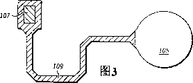
图3是根据这里的教导制造的再分配导体109的顶视图。再分配导体109沿着旋绕的路径从内部接触焊盘107行进到凸起触点105。优选地示出为凸起触点105的焊盘是圆形的,且形成球形焊料球的基部(例如,见图9)。
由于再分配导体是旋绕的,因此其具有固有可挠性,非常像盘绕的听筒软线,允许其伸长、扭曲和其它的吸收应变,而不会发生导致电性功能损失的铜引线断开。事实上,已经发现,与由相同材料制造并具有相似尺寸的非旋绕导体相比,使用旋绕的再分配导体改善导体应变的能力要多出6倍。
再分配导体109所沿的旋绕路径可以是蜿蜒形、正弦形、S-形或不规则形,或可通过曲线和具有角度的段(angled segment)的各种组合来描述。例如,曲线可由连接到一起的很多线段组成以接近弧度。为了简化设计,可以将三个线段连接到一起以实现90o弯曲。优选地,再分配导体不含有尖锐的(如90o)弯曲,而是利用较大数量的更多的钝角的弯曲以共同实现相同的效果,这是由于其减少了在尖锐的拐角处发生的应力集中点。因此,弯曲具有通常在约115o至约155o范围内的角度,优选在约125o至约145o范围内,且更优选在约130o至约140o的范围内。最优选地,弯曲具有约135o的角度。
如上面提出的,再分配导体可直接生长于具有如TiW/Cu的金属化层的聚酰亚胺层上,其与下部(通常为聚酰亚胺)钝化层形成易分离的接合。在超高应力下,超过了金属化脱离层和钝化层之间的剥离力,因此再分配导体可从聚酰亚胺层得以脱离。这种脱离为旋绕的再分配导体提供了移动的灵活性,且由此允许再分配导体移位,因而缓解了在仍贴附的剩余再分配导体之上的应力。当应力超出剥离力时,出现了其它再分配导体的分层。分层一直持续,直到在管芯上的残留应力降低到剥离力以下的水平。再分配导体通常在截面上足够厚以使得其具有足够的机械强度,以避免在这种脱离之前或之后断裂。再分配层的厚度也赋予其更多的耐侵蚀性。相反,在图1中所示的那些现有技术的再分配导体中,导体通常厚度小于1微米,且不能通过其自身支撑任何巨大数量的应力或张力。事实上,为了提供侵蚀保护和提高机械完整性的目的,现有技术中普遍使用在再分配导体上方的第三钝化层。
根据这里的教导制造的再分配导体的厚度是可变的。然而,优选地,再分配导体足够厚(例如,至少约3微米厚,这是横跨其最薄的尺寸所测量的),以使该厚度可经受很大数量的应力和张力,并可耐侵蚀。虽然根据这里的教导制造的再分配导体的可能厚度不存在具体的上限限制,但是在某一点之后,从增长的厚度获得的一些机械上的益处被增长的成本和处理时间抵消了。因此,根据这里的教导制造的再分配导体在厚度上优选在约5至约20微米的范围内,更优选在约8至约16微米的范围内,和最优选在约10至约14微米的范围内,这是沿着穿过横向延伸部分的中心并与横向延伸部分成直角延伸的轴所测量的。
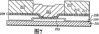
这里描述的再分配导体可通过多个不同的制造方法来实现。一种可能的方法在图4-8中说明。参考图4,提供其上具有接触焊盘203的管芯201。在一个实施例中,接触焊盘由铝或铝合金形成。该接触焊盘通常是集成半导体器件的顶部内部导体。将聚酰亚胺206和等离子体氮氧化物(PON)钝化层204设置在管芯上方和部分接触焊盘上方。然后,对钝化层图案化并曝光,由此经由开口207暴露出部分接触焊盘。然后,如图5中示出的将金属化层209溅射到获得的制品上。金属化层209包括两层:导电脱离层211和导电籽晶层213。在优选实施例中,脱离层包括TiW,而导电籽晶层包括铜。
然后,将旋涂光刻胶层217淀积在该结构上方。然后,图案化光刻胶,曝光并显影,以限定暴露出部分金属化层的开口219。暴露的金属化层部分在接触焊盘和部分钝化层上方延伸。
如图7中所示,在形成开口之后,将用于形成再分配导体221的金属(优选为铜)电镀到金属化层209的暴露部分上。如图8中所示,然后剥去光刻胶,和用适当的蚀刻移除暴露的金属化层209。例如,如果金属化层209包括TiW的导电脱离层211和铜的导电籽晶层213,则可使用喷雾酸工具,或可选地,在搅拌槽中,用亚氯酸盐或过硫酸铜蚀刻剂来移除导电籽晶层213,并可用热过氧化氢溶液来移除导电脱离层211。优选地,导电脱离层211和导电籽晶层213足够薄,以使只在短暂的暴露于这些蚀刻剂之后,就移除了这些层的暴露部分。而且,与导电脱离层211和导电籽晶层213相比,优选的是再分配导体221足够厚,以使得经过用于移除这些层的暴露部分的蚀刻剂之后基本不改变其尺寸。如在图10中描述的,蚀刻导电脱离层211和导电籽晶层213可导致在再分配导体221和凸起触点231下部的轻微数量的内切(undercutting)(见图10)。
图9是示出图8的再分配导体221的透视图,且因此示出在完成了图4-8中描述的步骤之后,器件呈现出怎样的样子。如这里可看见的,再分配导体221始于接触焊盘203和终止于凸起触点231,以旋绕形式延伸通过最终的聚酰亚胺钝化层206的表面。
用于完成器件的剩下的处理步骤在图10-14中描述。图10描述了器件在沿着图9的CURVE 10-10取得的截面中的样子,其沿着旋绕的再分配导体221的中心点,从紧随在接触焊盘203之后的点至凸起触点231。为了简化说明,将截面平坦化成单个平面,且器件的某些元件的尺寸已经减小了。
如图10中所示,处理进行到目前,器件包括其上具有铝接触焊盘203的管芯201。将聚酰亚胺206和等离子体氮氧化物(PON)204钝化层设置于管芯上方和部分接触焊盘203上方,和将包括TiW层211和铜层213的金属化层部分209设置于聚酰亚胺层206上方。
如图11中所示,然后将附加金属化层部分210溅射到管芯上方。尽管也可以使用其它的材料和数量的层,但是优选地,附加金属化层部分210包括TiW层215和Cu层217。然后,淀积光刻胶层222,如图12中所示。该光刻胶足够厚(通常约15微米的厚度)以涂覆在再分配导体221上方。如图12中所示,然后对光刻胶曝光,显影并烘焙以暴露出凸起触点231附近的一部分再分配导体。然后通过使用光刻胶作为蚀刻掩模蚀刻金属,将TiW层215和Cu层217从暴露的一部分再分配导体处除去。然后剥去光刻胶,如图13中所示。
然后,可使用例如可以是亚氯酸盐或过硫酸铜蚀刻剂的清洗剂以准备进行再分配导体221的凸起的模板制造。如图14中所示,清洗剂完全地移除了在TiW层215上方的薄Cu层217(见图13)。然后用O2,等离子体或通过其它的方式对获得的结构进行清洗,以移除由前述的处理步骤遗留的残留物。然后可将常规的焊料凸起金属,如可用为焊膏的共晶SnPb或合适的无铅焊料,用在模板凸起制造操作中,以将焊料凸起制造于凸起触点231上。在随后的回流期间,焊料219润湿暴露的一部分再分配导体231,但是不润湿由TiW层215覆盖的部分再分配导体221。焊料219直接在再分配导体221上形成球形的凸起,如图14中所示。
图10-14中描述的方法允许使用再分配导体而不必使用第三钝化层作为焊料掩模,这是由于,如上所述,TiW层用作了焊料掩模。而且,TiW层薄且形成再分配导体的整体部分,且能够由此沿着再分配导体移动和扭曲而不断裂。
图14中示出的器件具有多个优点,其中的一些已经提及了。最值得注意的,虽然现有技术器件通常需要使用未充满的材料或附加钝化层以容许在倒装芯片组件中的CTE应力差,但是由于这里描述的器件可以通过经历轻微的脱离和移动来实现CTE应力差减小以减小应力,因此这里这些器件不需要使用未充满的材料,。在图15中说明了这个效果。因此,当根据这里的教导制造的器件贴附到在PCB241或其它的安装衬底上的接合焊盘243上时,通过存在于TiW层211和聚酰亚胺钝化电介质206之间的易分离连接处的分层,就可以缓解PCB和管芯之间的CTE应力差,这是由于两层之间的较弱的连接引起了该连接相对不牢固。因此,如图15中所示,在应力下,再分配导体221从聚酰亚胺表面206剥离。由于聚酰亚胺钝化层206具有钝化的表面,因此分层并不改变在管芯201中的任一个器件的电学特性。而且,由于再分配导体221较厚,因此再分配导体221相对坚固,并且且其蜿蜒形状允许其表现得与可以伸长或缩短但并不造成机械或电性损坏的蛇形管相类似。
这里提供的管芯安装有具有独特设计以允许其经受CTE应力差的再分配导体,因此该管芯不需要使用未充满材料。设计再分配导体以使得其能从管芯表面分离并能够伸长或缩短,以容许管芯和PCB衬底之间的CTE应力差。
本发明上面的描述是说明性的,且不意指为限定性的。由此,将意识到,可以对上述的实施例作出各种添加、替换和修改,而不超出本发明的范围。例如,优选再分配导体是旋绕的,这是由于这样做可以获得同样能够减小应力的更紧凑的配置。然而,本领域技术人员将意识到通过使用足够长度的线性再分配导体也可以实现相类似的效果,其中再分配导体可拆卸地贴附到下部钝化层,如这里描述的。因此,本发明的范围只是参考附加的权利要求来构建。
Claims (40)
1.一种器件,包括:
半导体衬底,其上具有接触焊盘;
再分配导体,其具有与接触焊盘电连接的基部部分,并具有横向延伸部分;和
设置在所述横向延伸部分和所述衬底之间的钝化层;
其中所述横向延伸部分形成与钝化层的易分离接合。
2.如权利要求1的器件,其中横向延伸部分是旋绕的。
3.如权利要求1的器件,其中横向延伸部分终止于凸起的触点,且其中横向延伸部分在从基部部分向凸起的触点行进中,至少两次改变方向。
4.如权利要求1的器件,其中横向延伸部分终止于凸起的触点,且其中横向延伸部分在从基部部分向凸起的触点行进中,至少三次改变方向。
5.如权利要求1的器件,其中横向延伸部分实质上是蜿蜒形状。
6.如权利要求1的器件,其中横向延伸部分包括以约115o至约155o范围内的角度连接在一起的多个线段。
7.如权利要求1的器件,其中横向延伸部分包括以约125o至约145o范围内的角度连接在一起的多个线段。
8.如权利要求1的器件,其中横向延伸部分具有至少约3微米的平均最小厚度,这是沿着穿过横向延伸部分的中心并与横向延伸部分成直角延伸的轴所测量的。
9.如权利要求1的器件,其中横向延伸部分具有至少约8至约16微米范围内的平均最小厚度,这是沿着穿过横向延伸部分的中心并与横向延伸部分成直角延伸的轴所测量的。
10.如权利要求1的器件,还包括形成于焊料凸起,所述焊料凸起形成在与所述基部部分相对的再分配导体的端部附近,并与该端部电性连接的。
11.如权利要求1的器件,还包括与再分配导体电性连接的凸起的触点,和与所述的凸起的触点接触的PCB衬底。
12.如权利要求11的器件,其中PCB衬底通过开口空间与再分配导体相分离。
13.如权利要求1的器件,还包括设置在横向延伸部分和钝化层之间的脱离层。
14.如权利要求13的器件,其中脱离层包括TiW。
15.一种器件,包括:
具有接触焊盘的半导体衬底;
钝化层;
再分配导体,其具有与接触焊盘电性连接的基部部分和在所述的钝化层上方延伸的横向延伸部分;和
设置在所述钝化层和所述横向延伸部分的脱离层。
16.如权利要求15的器件,其中所述的脱离层包括TiW。
17.如权利要求16的器件,其中再分配导体包括铜。
18.如权利要求15的器件,还包括形成于与基部部分相对的再分配导体的端部附近并与其电性连接的焊料凸起。
19.如权利要求18的器件,其中再分配导体提供有在所述焊料凸起附近的焊料掩模。
20.如权利要求18的器件,还包括与所述焊料凸起接触的安装衬底,并且其中安装衬底通过开口空间与再分配导体相分离。
21.如权利要求15的器件,其中横向延伸部分具有至少约3微米的平均最小厚度,这是沿着穿过横向延伸部分的中心且与横向延伸部分成直角延伸的轴所测量的。
22.如权利要求15的器件,其中横向延伸部分具有在约8至约16微米范围内的平均最小厚度,这是通过穿过横向延伸部分的中心并与横向延伸部分成直角延伸的轴所测量的。
23.一种用于制造半导体器件的方法,包括以下步骤:
提供具有接触焊盘的半导体衬底;
在衬底上方形成钝化层,并对该钝化层进行图案化以暴露出至少部分接触焊盘;和
形成再分配导体,所述再分配导体具有与接触焊盘电性连接的基部部分,并具有旋绕的、在钝化层上方延伸的横向延伸部分;
其中横向延伸部分形成与钝化层的易分离接合。
24.如权利要求23的方法,还包括在钝化层上方形成脱离层的步骤。
25.如权利要求24的方法,其中脱离层设置在再分配导体和钝化层之间。
26.如权利要求24的方法,其中脱离层包括TiW。
27.如权利要求23的方法,其中再分配导体由以下步骤形成:
在钝化层上方淀积金属化层;
在金属化层上方淀积并图案化光刻胶层,以暴露出部分金属化层;和
将再分配导体材料电镀到暴露出的部分金属化层上。
28.如权利要求27的方法,其中将再分配导体的材料电镀为至少约3微米的最小厚度,这是沿着穿过横向延伸部分的中心并与横向延伸部分成直角延伸的轴所测量的。
29.一种用于制造半导体器件的方法,包括以下步骤:
提供具有接触焊盘的半导体衬底;
在衬底上方淀积钝化层并图案化钝化层,以暴露出至少部分接触焊盘;
在钝化层上方淀积金属化层;
在金属化层上方淀积光刻胶层,并图案化光刻胶层,以暴露出在接触焊盘附近的至少部分金属化层;和
将再分配导体电镀到金属化层的暴露部分上,以使得再分配导体具有与接触焊盘电性连接的基部部分和横向延伸部分。
30.如权利要求29的方法,其中再分配导体具有至少约3微米的平均最小厚度,这是沿着穿过横向延伸部分的中心并与横向延伸部分成直角延伸的轴所测量的。
31.如权利要求29的方法,其中图案化光刻胶层以使得横向延伸部分是旋绕的。
32.如权利要求29的方法,其中金属化层形成与钝化层的易分离接合。
33.如权利要求29的方法,其中图案化光刻胶层,以使得横向延伸部分实质上为蜿蜒形状。
34.如权利要求29的方法,其中横向延伸部分具有在约8至约16微米范围内的最小平均厚度,这是沿着穿过横向延伸部分中心并与横向延伸部分成直角延伸的轴所测量的。
35.如权利要求29的方法,还包括形成焊料凸起的步骤,所述焊料凸起电性连接至与基部部分相对的再分配导体的端部附近的再分配导体。
36.如权利要求29的方法,其中横向延伸部分连接至焊料连接,且适合于通过从第一钝化层分层降低施加到焊料连接的应力。
37.如权利要求29的方法,其中横向延伸部分连接至焊料连接,且其中在钝化层和金属化层之间的接合足够易分离,以使得当将足够的应力施加到焊料连接时,横向延伸部分与钝化层分离。
38.如权利要求29的方法,其中再分配导体包括铜,其中金属化层包括第一TiW层和第二铜层,且其中钝化层包括聚酰亚胺。
39.如权利要求29的方法,还包括在部分再分配导体上方淀积去湿剂的步骤。
40.如权利要求39的方法,其中金属化层和去湿剂都包括TiW。
Applications Claiming Priority (2)
| Application Number | Priority Date | Filing Date | Title |
|---|---|---|---|
| US10/631,102 | 2003-07-31 | ||
| US10/631,102 US6790759B1 (en) | 2003-07-31 | 2003-07-31 | Semiconductor device with strain relieving bump design |
Publications (1)
| Publication Number | Publication Date |
|---|---|
| CN1926674A true CN1926674A (zh) | 2007-03-07 |
Family
ID=32927915
Family Applications (1)
| Application Number | Title | Priority Date | Filing Date |
|---|---|---|---|
| CNA2004800178066A Pending CN1926674A (zh) | 2003-07-31 | 2004-07-13 | 具有减小应力的凸起设计的半导体器件 |
Country Status (6)
| Country | Link |
|---|---|
| US (2) | US6790759B1 (zh) |
| JP (1) | JP2007502530A (zh) |
| KR (1) | KR101106832B1 (zh) |
| CN (1) | CN1926674A (zh) |
| TW (1) | TWI354362B (zh) |
| WO (1) | WO2005013319A2 (zh) |
Cited By (5)
| Publication number | Priority date | Publication date | Assignee | Title |
|---|---|---|---|---|
| US8059914B2 (en) | 2006-11-28 | 2011-11-15 | Shenzhen Mindray Bio-Medical Electronics Co., Ltd. | Method and apparatus for preprocessing ultrasound imaging |
| CN101969053B (zh) * | 2008-05-16 | 2012-12-26 | 精材科技股份有限公司 | 半导体装置及其制造方法 |
| CN102842547A (zh) * | 2011-06-24 | 2012-12-26 | 台湾积体电路制造股份有限公司 | 用于改善布线和减小封装应力的接合焊盘设计 |
| CN105097564A (zh) * | 2014-05-12 | 2015-11-25 | 中芯国际集成电路制造(上海)有限公司 | 芯片封装结构的处理方法 |
| CN108369935A (zh) * | 2015-11-27 | 2018-08-03 | 追踪有限公司 | 具有薄的焊料阻止层的电元器件和用于制造的方法 |
Families Citing this family (44)
| Publication number | Priority date | Publication date | Assignee | Title |
|---|---|---|---|---|
| US7115998B2 (en) * | 2002-08-29 | 2006-10-03 | Micron Technology, Inc. | Multi-component integrated circuit contacts |
| US20040222511A1 (en) * | 2002-10-15 | 2004-11-11 | Silicon Laboratories, Inc. | Method and apparatus for electromagnetic shielding of a circuit element |
| US7141883B2 (en) * | 2002-10-15 | 2006-11-28 | Silicon Laboratories Inc. | Integrated circuit package configuration incorporating shielded circuit element structure |
| JP3678239B2 (ja) * | 2003-06-30 | 2005-08-03 | セイコーエプソン株式会社 | 半導体装置及びその製造方法、回路基板並びに電子機器 |
| TWI260078B (en) * | 2003-08-21 | 2006-08-11 | Advanced Semiconductor Eng | Chip structure |
| US7425759B1 (en) * | 2003-11-20 | 2008-09-16 | Bridge Semiconductor Corporation | Semiconductor chip assembly with bumped terminal and filler |
| DE102004035080A1 (de) * | 2004-05-27 | 2005-12-29 | Infineon Technologies Ag | Anordnung zur Verringerung des elektrischen Übersprechens auf einem Chip |
| US7423346B2 (en) * | 2004-09-09 | 2008-09-09 | Megica Corporation | Post passivation interconnection process and structures |
| US7812441B2 (en) | 2004-10-21 | 2010-10-12 | Siliconix Technology C.V. | Schottky diode with improved surge capability |
| US7394158B2 (en) * | 2004-10-21 | 2008-07-01 | Siliconix Technology C.V. | Solderable top metal for SiC device |
| US7834376B2 (en) | 2005-03-04 | 2010-11-16 | Siliconix Technology C. V. | Power semiconductor switch |
| US9419092B2 (en) * | 2005-03-04 | 2016-08-16 | Vishay-Siliconix | Termination for SiC trench devices |
| JP2006303452A (ja) * | 2005-03-25 | 2006-11-02 | Sanyo Electric Co Ltd | 半導体装置及びその製造方法 |
| US20060264021A1 (en) * | 2005-05-17 | 2006-11-23 | Intel Corporation | Offset solder bump method and apparatus |
| US7319043B2 (en) * | 2005-09-26 | 2008-01-15 | Advanced Chip Engineering Technology Inc. | Method and system of trace pull test |
| US7501924B2 (en) * | 2005-09-30 | 2009-03-10 | Silicon Laboratories Inc. | Self-shielding inductor |
| US8368165B2 (en) * | 2005-10-20 | 2013-02-05 | Siliconix Technology C. V. | Silicon carbide Schottky diode |
| DE102005055402A1 (de) * | 2005-11-17 | 2007-05-31 | Infineon Technologies Ag | Verfahren zur Herstellung einer Umverdrahtung auf Substraten/einem Wafer |
| US7831434B2 (en) * | 2006-01-20 | 2010-11-09 | Microsoft Corporation | Complex-transform channel coding with extended-band frequency coding |
| JP2007258438A (ja) * | 2006-03-23 | 2007-10-04 | Fujitsu Ltd | 半導体装置及びその製造方法 |
| US20070246805A1 (en) * | 2006-04-25 | 2007-10-25 | Ligang Zhang | Multi-die inductor |
| EP2047514A4 (en) | 2006-07-31 | 2010-12-01 | Vishay Siliconix | MOLYBDENUM BARRIER METAL FOR SIC SCHOTTKY DIODE AND METHOD FOR MANUFACTURING THE SAME |
| JP4354469B2 (ja) * | 2006-08-11 | 2009-10-28 | シャープ株式会社 | 半導体装置および半導体装置の製造方法 |
| US7524731B2 (en) * | 2006-09-29 | 2009-04-28 | Freescale Semiconductor, Inc. | Process of forming an electronic device including an inductor |
| US7834449B2 (en) * | 2007-04-30 | 2010-11-16 | Broadcom Corporation | Highly reliable low cost structure for wafer-level ball grid array packaging |
| TWI364804B (en) * | 2007-11-14 | 2012-05-21 | Ind Tech Res Inst | Wafer level sensor package structure and method therefor |
| US9345148B2 (en) * | 2008-03-25 | 2016-05-17 | Stats Chippac, Ltd. | Semiconductor device and method of forming flipchip interconnection structure with bump on partial pad |
| US7759137B2 (en) * | 2008-03-25 | 2010-07-20 | Stats Chippac, Ltd. | Flip chip interconnection structure with bump on partial pad and method thereof |
| US8809182B2 (en) | 2008-05-01 | 2014-08-19 | International Business Machines Corporation | Pad cushion structure and method of fabrication for Pb-free C4 integrated circuit chip joining |
| TWI450371B (zh) * | 2008-05-16 | 2014-08-21 | Xintec Inc | 半導體裝置及其製造方法 |
| US9165841B2 (en) * | 2008-09-19 | 2015-10-20 | Intel Corporation | System and process for fabricating semiconductor packages |
| US9164404B2 (en) | 2008-09-19 | 2015-10-20 | Intel Corporation | System and process for fabricating semiconductor packages |
| DE102008042824B4 (de) * | 2008-10-14 | 2022-01-27 | Robert Bosch Gmbh | Elektrischer Leiter und Verfahren zur Herstellung eines elektrischen Leiters |
| US7938016B2 (en) * | 2009-03-20 | 2011-05-10 | Freescale Semiconductor, Inc. | Multiple layer strain gauge |
| TWI367697B (en) * | 2009-08-17 | 2012-07-01 | Nan Ya Printed Circuit Board | Printed circuit board and fabrication method thereof |
| US8227333B2 (en) * | 2010-11-17 | 2012-07-24 | International Business Machines Corporation | Ni plating of a BLM edge for Pb-free C4 undercut control |
| US8648664B2 (en) | 2011-09-30 | 2014-02-11 | Silicon Laboratories Inc. | Mutual inductance circuits |
| US8847369B2 (en) * | 2012-07-20 | 2014-09-30 | Taiwan Semiconductor Manufacturing Company, Ltd. | Packaging structures and methods for semiconductor devices |
| US9609752B1 (en) * | 2013-03-15 | 2017-03-28 | Lockheed Martin Corporation | Interconnect structure configured to control solder flow and method of manufacturing of same |
| US9668352B2 (en) | 2013-03-15 | 2017-05-30 | Sumitomo Electric Printed Circuits, Inc. | Method of embedding a pre-assembled unit including a device into a flexible printed circuit and corresponding assembly |
| US8998454B2 (en) | 2013-03-15 | 2015-04-07 | Sumitomo Electric Printed Circuits, Inc. | Flexible electronic assembly and method of manufacturing the same |
| CN106233460A (zh) * | 2014-03-10 | 2016-12-14 | 德卡技术股份有限公司 | 包括加厚的再分布层的半导体器件及其制造方法 |
| TWI646877B (zh) * | 2018-03-12 | 2019-01-01 | Chipbond Technology Corporation | 軟性電路基板之佈線結構 |
| US11728308B2 (en) | 2021-04-26 | 2023-08-15 | Nxp B.V. | Semiconductor device under bump structure and method therefor |
Family Cites Families (8)
| Publication number | Priority date | Publication date | Assignee | Title |
|---|---|---|---|---|
| US5989936A (en) * | 1994-07-07 | 1999-11-23 | Tessera, Inc. | Microelectronic assembly fabrication with terminal formation from a conductive layer |
| US5518964A (en) * | 1994-07-07 | 1996-05-21 | Tessera, Inc. | Microelectronic mounting with multiple lead deformation and bonding |
| US5876859A (en) * | 1994-11-10 | 1999-03-02 | Vlt Corporation | Direct metal bonding |
| US6405429B1 (en) * | 1999-08-26 | 2002-06-18 | Honeywell Inc. | Microbeam assembly and associated method for integrated circuit interconnection to substrates |
| TW436933B (en) * | 1999-12-30 | 2001-05-28 | Taiwan Semiconductor Mfg | Method for defining a pattern |
| JP2001244372A (ja) * | 2000-03-01 | 2001-09-07 | Seiko Epson Corp | 半導体装置およびその製造方法 |
| US6362087B1 (en) * | 2000-05-05 | 2002-03-26 | Aptos Corporation | Method for fabricating a microelectronic fabrication having formed therein a redistribution structure |
| US6743660B2 (en) * | 2002-01-12 | 2004-06-01 | Taiwan Semiconductor Manufacturing Co., Ltd | Method of making a wafer level chip scale package |
-
2003
- 2003-07-31 US US10/631,102 patent/US6790759B1/en not_active Expired - Lifetime
-
2004
- 2004-07-13 KR KR1020067002029A patent/KR101106832B1/ko not_active IP Right Cessation
- 2004-07-13 CN CNA2004800178066A patent/CN1926674A/zh active Pending
- 2004-07-13 WO PCT/US2004/022433 patent/WO2005013319A2/en active Application Filing
- 2004-07-13 JP JP2006521868A patent/JP2007502530A/ja active Pending
- 2004-07-30 US US10/909,124 patent/US7208841B2/en not_active Expired - Fee Related
- 2004-07-30 TW TW093122939A patent/TWI354362B/zh not_active IP Right Cessation
Cited By (7)
| Publication number | Priority date | Publication date | Assignee | Title |
|---|---|---|---|---|
| US8059914B2 (en) | 2006-11-28 | 2011-11-15 | Shenzhen Mindray Bio-Medical Electronics Co., Ltd. | Method and apparatus for preprocessing ultrasound imaging |
| CN101969053B (zh) * | 2008-05-16 | 2012-12-26 | 精材科技股份有限公司 | 半导体装置及其制造方法 |
| CN102842547A (zh) * | 2011-06-24 | 2012-12-26 | 台湾积体电路制造股份有限公司 | 用于改善布线和减小封装应力的接合焊盘设计 |
| CN102842547B (zh) * | 2011-06-24 | 2016-02-24 | 台湾积体电路制造股份有限公司 | 用于改善布线和减小封装应力的接合焊盘设计 |
| CN105097564A (zh) * | 2014-05-12 | 2015-11-25 | 中芯国际集成电路制造(上海)有限公司 | 芯片封装结构的处理方法 |
| CN105097564B (zh) * | 2014-05-12 | 2018-03-30 | 中芯国际集成电路制造(上海)有限公司 | 芯片封装结构的处理方法 |
| CN108369935A (zh) * | 2015-11-27 | 2018-08-03 | 追踪有限公司 | 具有薄的焊料阻止层的电元器件和用于制造的方法 |
Also Published As
| Publication number | Publication date |
|---|---|
| US7208841B2 (en) | 2007-04-24 |
| KR20060054382A (ko) | 2006-05-22 |
| US20050023680A1 (en) | 2005-02-03 |
| US6790759B1 (en) | 2004-09-14 |
| WO2005013319A3 (en) | 2006-09-08 |
| TWI354362B (en) | 2011-12-11 |
| WO2005013319A2 (en) | 2005-02-10 |
| TW200518308A (en) | 2005-06-01 |
| KR101106832B1 (ko) | 2012-01-19 |
| JP2007502530A (ja) | 2007-02-08 |
Similar Documents
| Publication | Publication Date | Title |
|---|---|---|
| CN1926674A (zh) | 具有减小应力的凸起设计的半导体器件 | |
| US10269750B2 (en) | Methods and apparatus of packaging semiconductor devices | |
| US6818545B2 (en) | Low fabrication cost, fine pitch and high reliability solder bump | |
| US7579694B2 (en) | Electronic devices including offset conductive bumps | |
| US5736456A (en) | Method of forming conductive bumps on die for flip chip applications | |
| KR100918129B1 (ko) | 본드 패드를 갖는 상호 결선 구조체 및 본드 패드 상의범프 사이트 형성 방법 | |
| US7132750B2 (en) | Semiconductor component having conductors with wire bondable metalization layers | |
| US20080050909A1 (en) | Top layers of metal for high performance IC's | |
| US20020185721A1 (en) | Chip size package having concave pattern in the bump pad area of redistribution patterns and method for manufacturing the same | |
| US20040040855A1 (en) | Method for low-cost redistribution and under-bump metallization for flip-chip and wafer-level BGA silicon device packages | |
| US8294264B2 (en) | Radiate under-bump metallization structure for semiconductor devices | |
| TW201201330A (en) | Plasma treatment for semiconductor devices | |
| US6563216B1 (en) | Semiconductor device having a bump electrode | |
| US7176117B2 (en) | Method for mounting passive components on wafer | |
| JP2006332694A (ja) | 半導体表面上に金属バンプを形成する方法 | |
| JP2003258014A (ja) | 半導体表面上に金属バンプを形成する方法 |
Legal Events
| Date | Code | Title | Description |
|---|---|---|---|
| C06 | Publication | ||
| PB01 | Publication | ||
| C10 | Entry into substantive examination | ||
| SE01 | Entry into force of request for substantive examination | ||
| C12 | Rejection of a patent application after its publication | ||
| RJ01 | Rejection of invention patent application after publication |
Open date: 20070307 |