CN1159001A - Probe, manufacture of same, and vertically operative type probe card assembly employing same - Google Patents
Probe, manufacture of same, and vertically operative type probe card assembly employing same Download PDFInfo
- Publication number
- CN1159001A CN1159001A CN97101852A CN97101852A CN1159001A CN 1159001 A CN1159001 A CN 1159001A CN 97101852 A CN97101852 A CN 97101852A CN 97101852 A CN97101852 A CN 97101852A CN 1159001 A CN1159001 A CN 1159001A
- Authority
- CN
- China
- Prior art keywords
- probe
- plate
- contact site
- bending part
- circuit board
- Prior art date
- Legal status (The legal status is an assumption and is not a legal conclusion. Google has not performed a legal analysis and makes no representation as to the accuracy of the status listed.)
- Granted
Links
- 239000000523 sample Substances 0.000 title claims abstract description 477
- 238000004519 manufacturing process Methods 0.000 title claims description 14
- 239000004065 semiconductor Substances 0.000 claims abstract description 47
- 238000005452 bending Methods 0.000 claims description 158
- 238000000034 method Methods 0.000 claims description 25
- 238000010438 heat treatment Methods 0.000 claims description 22
- 230000008018 melting Effects 0.000 claims description 18
- 238000002844 melting Methods 0.000 claims description 18
- 239000011324 bead Substances 0.000 claims description 15
- 238000009434 installation Methods 0.000 claims description 9
- 238000009413 insulation Methods 0.000 claims description 9
- 229920005989 resin Polymers 0.000 claims description 9
- 239000011347 resin Substances 0.000 claims description 9
- 238000007747 plating Methods 0.000 claims description 7
- 239000011810 insulating material Substances 0.000 claims description 5
- 238000010257 thawing Methods 0.000 claims description 5
- 238000000429 assembly Methods 0.000 claims description 4
- 230000000712 assembly Effects 0.000 claims description 4
- 238000010891 electric arc Methods 0.000 claims description 4
- 230000005855 radiation Effects 0.000 claims description 3
- 229910000679 solder Inorganic materials 0.000 claims description 3
- 239000000725 suspension Substances 0.000 claims description 3
- 239000008188 pellet Substances 0.000 claims 1
- 230000008859 change Effects 0.000 description 21
- WFKWXMTUELFFGS-UHFFFAOYSA-N tungsten Chemical compound [W] WFKWXMTUELFFGS-UHFFFAOYSA-N 0.000 description 16
- 229910052721 tungsten Inorganic materials 0.000 description 16
- 239000010937 tungsten Substances 0.000 description 16
- 230000008569 process Effects 0.000 description 9
- 230000000694 effects Effects 0.000 description 8
- 238000003466 welding Methods 0.000 description 7
- RYGMFSIKBFXOCR-UHFFFAOYSA-N Copper Chemical compound [Cu] RYGMFSIKBFXOCR-UHFFFAOYSA-N 0.000 description 6
- 238000010586 diagram Methods 0.000 description 6
- 238000005259 measurement Methods 0.000 description 6
- 230000009471 action Effects 0.000 description 5
- 229910052751 metal Inorganic materials 0.000 description 5
- 239000002184 metal Substances 0.000 description 5
- KDLHZDBZIXYQEI-UHFFFAOYSA-N Palladium Chemical compound [Pd] KDLHZDBZIXYQEI-UHFFFAOYSA-N 0.000 description 4
- 239000004411 aluminium Substances 0.000 description 4
- 229910052782 aluminium Inorganic materials 0.000 description 4
- XAGFODPZIPBFFR-UHFFFAOYSA-N aluminium Chemical compound [Al] XAGFODPZIPBFFR-UHFFFAOYSA-N 0.000 description 4
- 239000011889 copper foil Substances 0.000 description 4
- 238000005516 engineering process Methods 0.000 description 4
- 238000005530 etching Methods 0.000 description 4
- 239000000463 material Substances 0.000 description 4
- BASFCYQUMIYNBI-UHFFFAOYSA-N platinum Chemical compound [Pt] BASFCYQUMIYNBI-UHFFFAOYSA-N 0.000 description 4
- PNEYBMLMFCGWSK-UHFFFAOYSA-N Alumina Chemical compound [O-2].[O-2].[O-2].[Al+3].[Al+3] PNEYBMLMFCGWSK-UHFFFAOYSA-N 0.000 description 3
- 239000003963 antioxidant agent Substances 0.000 description 3
- 230000003078 antioxidant effect Effects 0.000 description 3
- 235000006708 antioxidants Nutrition 0.000 description 3
- 230000015572 biosynthetic process Effects 0.000 description 3
- 239000003822 epoxy resin Substances 0.000 description 3
- 238000000227 grinding Methods 0.000 description 3
- 230000006698 induction Effects 0.000 description 3
- 238000003475 lamination Methods 0.000 description 3
- 229920000647 polyepoxide Polymers 0.000 description 3
- 238000012545 processing Methods 0.000 description 3
- IJGRMHOSHXDMSA-UHFFFAOYSA-N Atomic nitrogen Chemical compound N#N IJGRMHOSHXDMSA-UHFFFAOYSA-N 0.000 description 2
- PXHVJJICTQNCMI-UHFFFAOYSA-N Nickel Chemical compound [Ni] PXHVJJICTQNCMI-UHFFFAOYSA-N 0.000 description 2
- 239000004642 Polyimide Substances 0.000 description 2
- 238000013459 approach Methods 0.000 description 2
- 230000008901 benefit Effects 0.000 description 2
- 230000005540 biological transmission Effects 0.000 description 2
- 239000007767 bonding agent Substances 0.000 description 2
- 238000004140 cleaning Methods 0.000 description 2
- 238000013461 design Methods 0.000 description 2
- 239000012467 final product Substances 0.000 description 2
- 239000011521 glass Substances 0.000 description 2
- 239000001307 helium Substances 0.000 description 2
- 229910052734 helium Inorganic materials 0.000 description 2
- SWQJXJOGLNCZEY-UHFFFAOYSA-N helium atom Chemical compound [He] SWQJXJOGLNCZEY-UHFFFAOYSA-N 0.000 description 2
- 230000001771 impaired effect Effects 0.000 description 2
- 238000003780 insertion Methods 0.000 description 2
- 230000037431 insertion Effects 0.000 description 2
- 229910052741 iridium Inorganic materials 0.000 description 2
- GKOZUEZYRPOHIO-UHFFFAOYSA-N iridium atom Chemical compound [Ir] GKOZUEZYRPOHIO-UHFFFAOYSA-N 0.000 description 2
- 239000001301 oxygen Substances 0.000 description 2
- 229910052760 oxygen Inorganic materials 0.000 description 2
- 238000012856 packing Methods 0.000 description 2
- 229910052763 palladium Inorganic materials 0.000 description 2
- 239000004033 plastic Substances 0.000 description 2
- 229920003023 plastic Polymers 0.000 description 2
- 229910052697 platinum Inorganic materials 0.000 description 2
- 238000005498 polishing Methods 0.000 description 2
- 229920001721 polyimide Polymers 0.000 description 2
- 229910052703 rhodium Inorganic materials 0.000 description 2
- 239000010948 rhodium Substances 0.000 description 2
- MHOVAHRLVXNVSD-UHFFFAOYSA-N rhodium atom Chemical compound [Rh] MHOVAHRLVXNVSD-UHFFFAOYSA-N 0.000 description 2
- 239000004575 stone Substances 0.000 description 2
- 229910017083 AlN Inorganic materials 0.000 description 1
- PIGFYZPCRLYGLF-UHFFFAOYSA-N Aluminum nitride Chemical compound [Al]#N PIGFYZPCRLYGLF-UHFFFAOYSA-N 0.000 description 1
- 208000019901 Anxiety disease Diseases 0.000 description 1
- 241000218202 Coptis Species 0.000 description 1
- 235000002991 Coptis groenlandica Nutrition 0.000 description 1
- 208000037656 Respiratory Sounds Diseases 0.000 description 1
- 229910052581 Si3N4 Inorganic materials 0.000 description 1
- XUIMIQQOPSSXEZ-UHFFFAOYSA-N Silicon Chemical compound [Si] XUIMIQQOPSSXEZ-UHFFFAOYSA-N 0.000 description 1
- BQCADISMDOOEFD-UHFFFAOYSA-N Silver Chemical compound [Ag] BQCADISMDOOEFD-UHFFFAOYSA-N 0.000 description 1
- 238000010521 absorption reaction Methods 0.000 description 1
- 230000003064 anti-oxidating effect Effects 0.000 description 1
- 230000036506 anxiety Effects 0.000 description 1
- QVGXLLKOCUKJST-UHFFFAOYSA-N atomic oxygen Chemical compound [O] QVGXLLKOCUKJST-UHFFFAOYSA-N 0.000 description 1
- 229910052790 beryllium Inorganic materials 0.000 description 1
- ATBAMAFKBVZNFJ-UHFFFAOYSA-N beryllium atom Chemical compound [Be] ATBAMAFKBVZNFJ-UHFFFAOYSA-N 0.000 description 1
- 239000000919 ceramic Substances 0.000 description 1
- 239000002131 composite material Substances 0.000 description 1
- 229910052802 copper Inorganic materials 0.000 description 1
- 239000010949 copper Substances 0.000 description 1
- 230000008878 coupling Effects 0.000 description 1
- 238000010168 coupling process Methods 0.000 description 1
- 238000005859 coupling reaction Methods 0.000 description 1
- 238000005520 cutting process Methods 0.000 description 1
- 230000002950 deficient Effects 0.000 description 1
- 238000000280 densification Methods 0.000 description 1
- 230000005611 electricity Effects 0.000 description 1
- PCHJSUWPFVWCPO-UHFFFAOYSA-N gold Chemical compound [Au] PCHJSUWPFVWCPO-UHFFFAOYSA-N 0.000 description 1
- 229910052737 gold Inorganic materials 0.000 description 1
- 239000010931 gold Substances 0.000 description 1
- LNEPOXFFQSENCJ-UHFFFAOYSA-N haloperidol Chemical compound C1CC(O)(C=2C=CC(Cl)=CC=2)CCN1CCCC(=O)C1=CC=C(F)C=C1 LNEPOXFFQSENCJ-UHFFFAOYSA-N 0.000 description 1
- 239000012535 impurity Substances 0.000 description 1
- 239000011261 inert gas Substances 0.000 description 1
- 230000001788 irregular Effects 0.000 description 1
- 210000003127 knee Anatomy 0.000 description 1
- 238000004093 laser heating Methods 0.000 description 1
- 238000012423 maintenance Methods 0.000 description 1
- 238000001465 metallisation Methods 0.000 description 1
- 229910052752 metalloid Inorganic materials 0.000 description 1
- 150000002738 metalloids Chemical class 0.000 description 1
- 150000002739 metals Chemical class 0.000 description 1
- 229910052759 nickel Inorganic materials 0.000 description 1
- 229910052757 nitrogen Inorganic materials 0.000 description 1
- 229910000510 noble metal Inorganic materials 0.000 description 1
- 230000003647 oxidation Effects 0.000 description 1
- 238000007254 oxidation reaction Methods 0.000 description 1
- 238000004663 powder metallurgy Methods 0.000 description 1
- 239000012858 resilient material Substances 0.000 description 1
- 230000000630 rising effect Effects 0.000 description 1
- 229910052710 silicon Inorganic materials 0.000 description 1
- 239000010703 silicon Substances 0.000 description 1
- HQVNEWCFYHHQES-UHFFFAOYSA-N silicon nitride Chemical compound N12[Si]34N5[Si]62N3[Si]51N64 HQVNEWCFYHHQES-UHFFFAOYSA-N 0.000 description 1
- 229910052709 silver Inorganic materials 0.000 description 1
- 239000004332 silver Substances 0.000 description 1
- 125000006850 spacer group Chemical group 0.000 description 1
- 230000002269 spontaneous effect Effects 0.000 description 1
- 239000003351 stiffener Substances 0.000 description 1
Images


Classifications
-
- G—PHYSICS
- G01—MEASURING; TESTING
- G01R—MEASURING ELECTRIC VARIABLES; MEASURING MAGNETIC VARIABLES
- G01R1/00—Details of instruments or arrangements of the types included in groups G01R5/00 - G01R13/00 and G01R31/00
- G01R1/02—General constructional details
- G01R1/06—Measuring leads; Measuring probes
- G01R1/067—Measuring probes
- G01R1/07—Non contact-making probes
-
- G—PHYSICS
- G01—MEASURING; TESTING
- G01R—MEASURING ELECTRIC VARIABLES; MEASURING MAGNETIC VARIABLES
- G01R3/00—Apparatus or processes specially adapted for the manufacture or maintenance of measuring instruments, e.g. of probe tips
-
- G—PHYSICS
- G01—MEASURING; TESTING
- G01R—MEASURING ELECTRIC VARIABLES; MEASURING MAGNETIC VARIABLES
- G01R1/00—Details of instruments or arrangements of the types included in groups G01R5/00 - G01R13/00 and G01R31/00
- G01R1/02—General constructional details
- G01R1/06—Measuring leads; Measuring probes
- G01R1/067—Measuring probes
- G01R1/06711—Probe needles; Cantilever beams; "Bump" contacts; Replaceable probe pins
- G01R1/06716—Elastic
-
- G—PHYSICS
- G01—MEASURING; TESTING
- G01R—MEASURING ELECTRIC VARIABLES; MEASURING MAGNETIC VARIABLES
- G01R1/00—Details of instruments or arrangements of the types included in groups G01R5/00 - G01R13/00 and G01R31/00
- G01R1/02—General constructional details
- G01R1/06—Measuring leads; Measuring probes
- G01R1/067—Measuring probes
- G01R1/073—Multiple probes
- G01R1/07307—Multiple probes with individual probe elements, e.g. needles, cantilever beams or bump contacts, fixed in relation to each other, e.g. bed of nails fixture or probe card
- G01R1/07357—Multiple probes with individual probe elements, e.g. needles, cantilever beams or bump contacts, fixed in relation to each other, e.g. bed of nails fixture or probe card with flexible bodies, e.g. buckling beams
Abstract
A assembly configuration features in including: a plurality of probes having a buckling portion to buckle, upon a contact by an end of a contact portion onto an electrode of semiconductor integrated circuit; a first board provided with a first wiring pattern connected with a connecting portion of the probe; a second board removably fastened with the first board and provided with a second wiring pattern connected with the first wiring pattern; housing members mounted with the second board for holding the contact portion of the probe. Thereby, undesirable deviation of contact point by the probe is avoided and a suitable contact pressure is preferably kept, and further convenience in the work of exchanging damaged probes is brought about.
Description
The present invention relates to a kind of be used to the measure probe of SIC (semiconductor integrated circuit) electrical specification, the manufacturing of this probe and the vertical probe card assembly that uses this probe, this assembly has been avoided the contact of unnecessary hope and has been convenient to change probe.In No. the 5134365th, the United States Patent (USP) of on July 28th, 1992 approval, the notion of probe card assembly has been done explanation.
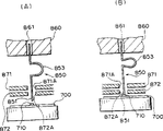
Vertical probe card assembly with reference to accompanying drawing 24 and 25 pairs of prior aries is described.
As shown in figure 24, the vertical probe card assembly of prior art is made up of the plate 860 of many probes 850, fastening probe 850 usefulness and the accommodating member 870 that is installed in plate 860 downsides.
Wherein, between contact site 851 and connecting portion 852, form the flexible part 853 that is generally horizontal U-shaped.As shown in figure 25, this flexible part 853 tends to bending or deflection, so that when contacting between contact site 851 and electrode 710, keeps necessary contact pressure.
Accommodating member 870 comprises two guide plates 871,872 that are provided with through hole 871A, 872A, and a pair of being used for carried out fastening wall 823 by 860 pairs of two guide plates 871,872 of plate.Through hole 871A, 872A in two guide plates 871,872 are used for inserting the contact site 851 of probe 850, and the position alignment of electrode 710 that makes it and SIC (semiconductor integrated circuit) 700 is for measurement.
On the other hand, be provided with predetermined circuit board (not shown) at the upside of plate 860, and be provided with the through hole 861 that can insert probe 850 connecting portions 852.As shown in figure 25, the connecting portion 852 that inserts in the through hole 861 is connected on the above-mentioned circuit board.
Yet the vertical probe card assembly of above-mentioned prior art exists following problem or difficulty:
During this vertical probe card assembly operate as normal hundreds of or several thousand probes are installed usually, but wearing and tearing or the probe that must change that damages have only several in the course of the work.
This replacing or the work that changes probe need earlier and will remove with the welding thing on the circuit board that couples together of connecting portion, and then will lift down on the probe slave plate.Yet the horizontal U font flexible part 853 of each probe 850 itself can not be pulled out by the through hole 861 of plate 860 because of steric hindrance.Must before changing probe 850, accommodating member 870 be unloaded for this reason.When can be when flexible part 853 places are cut probe, probe 850 might be lifted down and need not dismounting.Yet this method is damaged other probe that need not to change working properly sometimes, and various probes are housed in vertical probe card assembly, and it in fact also is impossible doing like this.
Even if it is possible changing the method for probe like this, need after on probe 850 slave plates 860, lifting down so the through hole 861 of new probe 850 slave plates 860 and through hole 871A, the 872A of two guide plates 871,872 are inserted, and not change probe consistent with other to make the height and position of contact site 851 of new probe, also to arrange the direction of flexible part 853, so that they do not contact mutually, and then connecting portion 852 and circuit board are coupled together by welding.Therefore, be equipped with in production in enormous quantities under the situation of probe card assembly of various probes, the work of changing probe is the labour-intensive type work that needs the anxiety that the skilled person very carefully operates.
And existing probe card assembly has such size: the vertical thickness of plate is about 6mm, and the vertical length of accommodating member is about 10mm, so the length of probe is about 20mm.Recently SIC (semiconductor integrated circuit) is making much progress aspect the use high speed signal, requires short as far as possible probe and circuit board conversely so that signal attenuation is reduced to minimum in advance with disturbing.Though wish further to shorten probe length, yet used probe length is at least 20mm in the existing vertical probe card assembly.
In addition, probe is generally made by the tungsten filament that the powder metallurgy tungsten bar draws.Therefore, the drawing of tungsten filament makes crackle or defective extend along probe length, partly be that contact site has the irregular trend of bigger formation so draw the processing of tungsten filament, thereby the probe contact site is than the external snotter of the easier attraction of other parts.
In order to overcome the problems referred to above, the probe that contacts with electrode is cleaned, so that the foreign impurity of contact site is removed.Perhaps earlier contact site is done circular.Yet the cleaning requirement time-based maintenance also causes using the operation of probe to delay, and circular for contact site is done, and it is very difficult must making correct semicircle at place, contact site end.And it also is difficult will handling various probes simultaneously, so just reduced production efficiency.
On the other hand, some electrodes are the semi-circular projection shape.These electrodes are applied to have the probe of flush end contact site, but this probe has changed the shape of end when cleaning, thereby are difficult to obtain correct measurement.
The object of the present invention is to provide a kind of employing length shorter, and, be suitable for the probe of this assembly in that the vertical probe card assembly of also being convenient to change the damage probe under the situation of various probes is housed, and the method for making this probe.
A kind of probe of the present invention, it is characterized in that: its shape is generally needle-like, and has one when touching the electrode of SIC (semiconductor integrated circuit) in its contact end, bend or the bending part of bending, wherein, described probe has the cross section that is generally circular, and its bending part is all thin than other parts except that the contact end; Contact site and bending part are made into linearity.A kind of process of making probe of the present invention is characterized in that: described process is used to make a kind of and the contacted probe of electrode SIC (semiconductor integrated circuit), and described process has the described step that is used for the contact site that contacts with electrode of heating and melting; And from melting the step that partly forms bead.
First vertical probe card assembly structure, it is characterized in that the probe that has one section bending part by many, described bending part bends when the probe contact site contacts with the electrode of SIC (semiconductor integrated circuit) or bending, to be provided with first plate, of the first circuit board that links to each other with the connecting portion of described probe removably fastening with described first plate and be provided with second plate of the second circuit board that links to each other with described first circuit board, and be used for the described probe contact site of clamping, form with the accommodating member that second plate is installed together.Wherein, described probe has the cross section that is generally circular, and its bending part is all thin than other parts except that the contact end; Contact site and bending part are made into linear; Described first plate is provided with and is used for the through hole that correspondent probe is inserted, and described second plate is provided with and is used for probe so that from space that the described first plate suspension status extends through.
Second vertical probe card assembly structure, it is characterized in that the measuring probe that is respectively equipped with bending part by many, described bending part when the electrode contact of probe contact site and SIC (semiconductor integrated circuit), take place bending, one be provided with first plate that is connected the circuit board that the end links to each other of described measuring probe, cover on described first plate and with its second removably fastening plate, and a plurality of being respectively equipped with inserting the end of contact site the set through hole of second plate, and the probe that the bending part of bending links to each other takes place when contacting with circuit board form.Wherein, described measuring probe and described linking probe have the cross section that is generally circular, and its bending part is all thin than other parts except that the contact end; Contact site and bending part are made into linear usually; Described first plate is provided with the through hole that is used to insert described measuring probe, and described second plate is provided with the circuit board of the rear end that is connected to the probe connecting portion that is used for the circuit connection.
The 3rd vertical probe card assembly structure, it is characterized in that the probe that is respectively equipped with contact site and bending part by many, bending, one take place and are provided with circuit board so that the plate of linking probe connecting portion at upside at least in described bending part when contact site contacts with the electrode of SIC (semiconductor integrated circuit), and are installed in described plate downside and are used for being formed with the supporting member of supporting probe.Wherein, each probe all has the cross section that is generally round, and its bending part is all thin than other parts except that the contact end; Described contact site and bending part are made into linear; Described plate is provided with the through hole that passes for probe; Described supporting member comprises: a plurality ofly make and be provided with a plurality of grooves in periphery by insulating material, be used for the bending of clamping probe partly in the probe support of inside grooves, be used for removably described probe support being separately fixed at the stationary installation of the downside of described plate.
The accompanying drawing simple declaration:
Fig. 1 is the front elevation of first probe of the present invention.
Fig. 2 is the front elevation that is specifically designed to the probe of the present invention of explaining the bending action.
Fig. 3 is the front elevation of second probe of the present invention.
Fig. 4 is the front elevation of the 3rd probe of the present invention.
Fig. 5 is used to explain the first operation synoptic diagram of making probe of the present invention.
Fig. 6 is used to explain the second operation synoptic diagram of making probe of the present invention.
Fig. 7 is used to explain the 3rd operation synoptic diagram of making probe of the present invention.
Fig. 8 is the longitudinal section that belongs to first vertical probe card assembly of the present invention.
Fig. 9 is the synoptic diagram of expression first probe card assembly action.
Figure 10 is the decomposing schematic representation of first probe card assembly.
Figure 11 is the stereographic map of the part excision of the first probe card assembly key component.
Figure 12 is the longitudinal section that belongs to second vertical probe card assembly of the present invention.
Figure 13 is the action synoptic diagram of the second probe card assembly key component.
Figure 14 is the longitudinal section that belongs to the 3rd vertical probe card assembly of the present invention.
Figure 15 is the decomposing schematic representation of the 3rd probe card assembly.
Figure 16 is the stereographic map that belongs to the part excision of the 4th vertical probe card assembly of the present invention.
Figure 17 is the decomposing schematic representation of four point probe card assembly.
Figure 18 is the longitudinal section that belongs to the 5th vertical probe card assembly of the present invention.
Figure 19 represents the schematic perspective view looked up from the 5th probe card assembly.
Figure 20 represents to be assemblied in the decomposing schematic representation of the supporting member in the 5th probe card assembly.
Figure 21 is contained in the cut-open view of annexation between plate in the 5th assembly and the probe connecting portion for explanation.
Figure 22 is the cut-open view of annexation between explanation probe support part and the probe.
The cut-open view that Figure 23 disposes in groove for the explanation probe.
Figure 24 is the longitudinal section that belongs to the vertical probe card assembly of conventional related.
Figure 25 is the cut-open view of expression conventional probe card assembly action, comprising figure (A) and (B).
In general, these 25 accompanying drawings can be divided into 4 classes: probe structure, the manufacturing of probe, probe card assembly structure, and correlation technique.
Fig. 1 to 4 wherein shows three embodiment (Fig. 1 represents first embodiment, and Fig. 3 represents second embodiment, and Fig. 4 represents the 3rd embodiment) in order to the expression probe structure.
Fig. 5 to 7 wherein shows three embodiment (Fig. 5 represents first embodiment, and Fig. 6 represents second embodiment, and Fig. 7 represents the 3rd embodiment) in order to the manufacturing of expression probe.
Fig. 8 to 23 is in order to expression probe card assembly structure, (Fig. 8 to 11 represents first embodiment, and Figure 12 to 13 represents second embodiment, and Figure 14 to 15 represents the 3rd embodiment wherein to show five embodiment, Figure 16 to 17 represents the 4th embodiment, and Figure 18 to 23 represents the 5th embodiment).
Figure 24 to 25 is in order to the expression correlation technique corresponding with the present invention.
Specific descriptions of the present invention and preferred embodiment are as follows.
The characteristic of probe
Below describe referring to figs. 1 through 4 pairs of probes of the present invention.As shown in Figure 1, the characteristics of first probe are that probe 100 is on the whole for line style, as a pin or spicule, its cross section is generally circle, and having bending part 120, this bending part is for thinner than other two connecting portions 110,130 except that contact site 110 ends, and stage portion 102S.
Another characteristics of probe 100 are certain situation of contact site 110 ends, although these are not concrete in Fig. 1, have done to replenish by Fig. 5 to 7.That is, a very little ball (seeing Fig. 7, wherein the size of not shown ball) is arranged in the end, and on ball, covered or plated that one deck is anti-oxidant, the metal of low resistance, high conductivity such as rhodium, palladium, iridium, platinum.After having covered these metals, contact jaw just can not allow the composition material aluminium of electrode 610 attached to above it, thus with the low susceptibility of 110 pairs of oxidations of contact site, last, the contact resistance value when measuring is stablized.
Manufacturing with probe of a bead
At the formed foremost bead of contact site 110, be by contact site 110 ends are heated, utilize and melt that part produces capillary method and row naturally.
To the heating and melting of the end of contact site 110 are laser radiations by as shown in Figure 5, or the radio-frequency coil heating by as shown in Figure 6, or undertaken by the arc discharge heating.
Under the situation of as shown in Figure 5 usefulness LASER HEATING, 1000 (0.25 mm dia) nickel plating tungsten filaments, its contact site 110 have been prepared specially by the electropolishing sharpening.These tungsten filaments are aligned to 20 * 50, and the space is 1 millimeter, and make contact site (shown in Fig. 5) regularly down.
Then YAG laser (for example 75 watts, beam diameter: about 0.1 to 0.2 millimeter) is shone in helium and accumulate on the contact site 110 with pulsating wave, wherein YAG laser two lasing light emitters of 45 degree about be positioned at focus on.Be about to contact site 110 heating and melting of tungsten filament W YAG laser wink and the focus of laser is moved on to next root tungsten filament, wherein the amount of thawing effect system is controlled by the impulse speed of YAG laser.
Come heating and melting preferably to adopt non-carrier of oxygen such as helium or nitrogen with YAG laser L, but under the situation of noble metal or anti-oxidation metal, can adopt air.
The situation of high-frequency induction heating, as shown in Figure 6, many tungsten filaments are arranged properly with appropriate intervals (about 1 millimeter usually).Wherein the contact site 110 (sharpening partly among Fig. 6) around tungsten filament is equipped with radio-frequency induction coil C, and this coil is switched on by high frequency electric source, and contact site 110 is carried out heating and melting.
In addition, can adopt arc discharge to heat to replace laser or high-frequency heating, the contact site 110 of tungsten filament W is carried out heating and melting, be preferably in certainly in the inert gas and carry out.
The technology of utilizing spontaneous surface tension to form bead has more than been described.Figure 7 shows that a substitute technology, promptly be ready to bead 150 in advance, and then and these beads 150 are heated and melted to tungsten filament or beryllium (berium) copper wire gets on.
Particularly, diameter is 0.5 millimeter a tungsten filament, grinds its end very sharp-pointed with the grinding stone that is rotating, and then bead 150 (diameter is 70 microns) is used the welding of hydrogen-oxygen flame heat on the tip of tungsten filament.
Another kind is exactly direct thawing method, i.e. clamping one has with the tungsten filament of a bead 150 contacted sharpening points and makes an electric current make its mutual thawing by two contactants under the state of clamping by this way.This method be suitable for the big batch manufacturing and cost lower.
Further describing of probe
Get back to probe 100 now, the importance of bending part 120 is described with reference to Fig. 2.As previously mentioned, bending part 120 is made into than other two the stage portion 120S that part is thinner or narrower except that contact site 110.Therefore, 110 places do the time spent effectively at contact site, bending part 120 will as the anticipation bending, as shown in Figure 2, and this specific character gives by grinding and polishing or electropolishing.
Connecting portion 130 is used for being connected with circuit board 310 or being fixed up 100.This connecting portion 130 is drawn the shape that is in line (seeing Fig. 1 or 2) from bending part 120, and (sees Figure 16 to 18 or Figure 21) when installing and fixing with plate 200, and connecting portion 130 will be partly, and (for example about 1 to 1.5 millimeter) stretches out plate 200.This extension can be clamped with the instrument (not shown).
The typical sizes of probe 100 is about 40 microns of bending part 120 diameters, long 3 millimeters; Contact site 110 is about 2.5 millimeters; Connecting portion 130 is about 3.5 millimeters.As described below, in the operation as too drastic amount be 0.1 millimeter, (too drastic amount is defined as: the vertical length that pushes that begins with the most advanced and sophisticated initial contact point of contact site from the electrode), then contact pressure is: 10-20g/cm
2And work as contact pressure is 15g/cm
2The time, the contact resistance between electrode and the probe 100 is estimated to be about 0.5 ohm.
The present invention does not get rid of it and only has sharpening point in contact site 110 ends and the probe 100 that do not have foregoing bead 150, because its bending part 120 under too drastic condition, plays a part stably to provide predetermined contact pressure.
Adopt the description of the vertical probe card assembly of above-mentioned probe
Description according to Fig. 8 to 11
Adopt first embodiment of the vertical probe card assembly of above-mentioned probe to be described hereinafter with reference to Fig. 8 to 11 pair.In the following description, will abbreviate " this kind assembly ", " this assembly " or " assembly " to term " vertical probe card assembly " as sometimes, if these abbreviations are considered to and can understand immediately.
First embodiment of vertical probe card assembly is characterised in that and comprises: a plurality of probes 100, this probe has and bends when the end of its contact site 110 contacts with the electrode 710 of SIC (semiconductor integrated circuit) 700 or the bending part 120 of bending, be provided with first plate 400 of the first circuit board 420 that is connected with probe 100 connecting portions 130, removably fixing with first plate 400 and be provided with second plate 500 of the second circuit board 520 that is connected with first circuit board 420, and the accommodating member of installing with second plate 500 that is used to control probe 100 contact sites 110 600; Wherein, probe 100 has the cross section that is generally circular, and its bending part 120 is thinner than other parts except that the end of contact site 110, and contact site 110 is made linear with bending part 120; Second plate 500 is provided with by opening 510, is inserted through for the probe 100 that is installed together with first plate 400, thereby forms an integral body.
At the upside of first plate 400, be provided with the first circuit board 420 that forms by the etching Copper Foil, be connected with the proving installation (not shown) for electrode 710 energisings of SIC (semiconductor integrated circuit) 700 and by means of probe 100.And its terminal with the form at junction surface 421 around through hole 410, with scolder 450 with connecting portion 130 connections of probe 100 or be fixed on this junction surface.Another terminal of first circuit board 420 is passed another through hole 430, and draws from the downside of first plate 400, and forms projection 422 there, as shown in figure 10.
Above-mentioned first plate 400 has fixed orifice 440 at the Qi Sijiao place, is used for removably fixing second plate 500.
The other end 522 of second circuit board 520 is exposed on second plate 500 with the form at junction surface, its exposure position is in first plate outside in the time of fixedly, be that the other end 522 of second circuit board 520 is exposed to position on second plate 500 and is confirmed as after first plate 400 and second plate 500 are fixing the external position that first plate 400 does not occupy as yet.
Like this, the end of first circuit board 420 is promptly connected by the end 521 with the second circuit board 520 at the place, junction surface of second plate, 500 upsides with the form of the projection 422 of first plate, 400 downsides.
Except that fixed orifice 530, second plate 500 also has the through hole 540 that is used for fixing accommodating member 600.Accommodating member 600 has and is being provided with the guide plate 610 of through hole 611 with probe 100 aligned position, and for the distance piece 620 of guide plate 610 and the fastening usefulness of second plate, 500 downsides.
The operating process of measuring the electrical specification of SIC (semiconductor integrated circuit) 700 by the invention described above assembly below is described.
This assembly be set at lifter 750 directly over.This lifter comes fastening by vacuum suction or configuration tablet (measuring piece).Lifter 750 moves up from its reference position with set measuring piece, wherein hoisting gear bottom (being shown in lifter 750 belows with dot-and-dash line among Fig. 8) is as two directions of arrow, vertically motion (in following accompanying drawing, omitting the hoisting gear bottom), the contact site 110 of probe 100 begins to contact with the electrode 710 of the SIC (semiconductor integrated circuit) that forms on pole plate, because of rising a bit of distance, lifter 750 produced too drastic amount then, because this too drastic effect makes probe 100 about behind the pressurized, the bending part 120 of probe 100 is appearance state as shown in Figure 9 just.Therefore kept required predetermined contact pressure.In this case, contact site 110 contacts of probe 100 also vertically push electrode 710, and do not have unnecessary slippage or slip on electrode 710, thereby have realized measuring accurately.
When the electrical specification of SIC (semiconductor integrated circuit) 700 was measured end, lifter 750 was reduced to its reference position, and has prepared new measuring piece by vacuum suction on lifter 750.
Illustrate now in this assembly of said structure how some probes are changed.
At first remove with first circuit board 420 connections or be bonded together, and the scolder 450 of the probe 100 that will change.Thereby the probe that makes the palpus transposing separates with first plate 400 or disconnects.The probe that to change upwards is pulled out to first plate, 400 outsides again, and this has just finished the dismounting work that must change probe.
New or replace probe 100 this assembly of packing into one.At first the through hole 410 by first plate 400 from top with new probe 100 plug-in packages.Wherein contact site 110 is inserted into the through hole 611 that passes the guide plate of aiming at above-mentioned through hole 410 610 certainly.The minimum point of the contact site 110 of new probe 100 is accurately located so that it and other probe 100 are on the same level, with scolder 450 connecting portion 130 is connected with the junction surface 421 of first circuit board 420 then or is bonded together.
After using one period stipulated time, need to allow to change all probes together under the situation of the many probes 100 of transposing with first plate 400.In this case, as shown in figure 10, remove screw 710, promptly allow first plate 400 and 500 disengagements of second plate and allow to change the first new plate 400 that new probe is housed, between first wherein new plate 400 and the second old plate 500, comprise that being electrically connected of proving installation (not shown) that extends to assembly outside will side by side finish by first circuit board 420 and second circuit board 520.
Explanation according to Figure 12 and 13
Another embodiment hereinafter with reference to Figure 12 and the vertical probe card assembly of 13 explanations.
This second assembly is different in the configuration aspects of second plate 500.Promptly the structure of second plate 500 in first embodiment as previously mentioned, for have a big central opening in inside, can both pass all probes at middle position.Second plate 500 then is provided with separately in a second embodiment, and what be used to make every probe can pass through through hole respectively.Therefore, second embodiment is different from first embodiment in this, and is then similar in others.
Specifically, the through hole 510 among second embodiment is aimed at the electrode 710 of SIC (semiconductor integrated circuit) 700 aspect the position.Promptly the through hole 510 of second plate 500 is positioned or is configured to and aims in vertical direction with the through hole 611 of the through hole 410 of first plate 400 and guide plate 610.
Wherein, the thickness of second plate 500 is designed to have enough or sufficient length, so that the bending part 120 of probe 100 is included in the thickness length.
Because bending part 120 bending after contact site 110 contacts at this second embodiment middle probe 100, each bending part 120 is controlled by the through hole 611 of the through hole 510 of second plate 500 and guide plate 610 and is fixed, thereby has avoided the contact between the bending part 120 of adjacent probe 100 fully.Therefore allow probe 100 is provided with De Gengmi.Though accompanying drawing 12 and 13 only shows two probes, on principle, made proof.
The step that probe 100 more changes jobs is roughly similar to the description of aforementioned first embodiment.Specifically, at first remove scolder 450,, then this probe 100 upwards is pulled out to first plate, 400 outsides so that probe 100 to be replaced is disconnected from first circuit board 420.Thereby it is removed from assembly fully.
With new or replace probe 2100 this assembly of packing into.At first with the through hole 410 of new probe 100, from the top plug-in package through first plate 400.Wherein contact site 110 can pass the through hole 611 of guide plate 610 certainly, and this through hole is aimed at top through hole 410.The minimum point of the contact site 110 of new probe 100 is accurately located or being on the par with other probe 100 aspect the height, is connected with the chamfered section 421 of first circuit board 420 with the end of scolder 450 with connecting portion 130 then.
After using one period stipulated time, need to allow to change all probes together under the situation of the many probes 100 of transposing with first plate 400.In this case, remove screw 710S and promptly allow first plate 400 and second plate 500 to throw off, and allow replacing that new probe, the first new plate 400 are housed.The joint of the first new plate 400 should comprise the through hole 510 of each probe 100 insertions second plate 500 and the through hole 611 of guide plate 610.
In this assembly, the through hole 510 of second plate 500 is added on the through hole 410 of first plate 400.So, probe 100 inserts the work of going in the through hole 410 of first plate 400, goes to bring convenience with making thereafter the end of the contact site 110 of probe 100 inserted in the through hole 611 of guide plate 610.The unique effect of Here it is this embodiment, and see on the whole, made things convenient for probe more to change jobs.
As shown in figure 13, in this assembly of this embodiment, permission is designed to be positioned at the connecting hole that first and second plates 400,500 extend aligning with the bending part 120 of probe 100, and being different from as shown in figure 12 situation, the through hole 510 that wherein is used for bending part 120 only forms in the thickness of second plate 500.
Under the situation of Figure 13, the through hole 410 of first plate 400 is independent of other adjacent hole with the through hole 510 of second plate 500 and is connected, so the probe of having avoided inserting in the adjacent holes 100 is in contact with one another under the bending state, and can be placed in the through hole 410 of first plate 400 bending part 120 and still be placed on the selection of carrying out in the through hole 510 of second plate 500, thereby when adjusting the synthetic contact force of essential realization, determine how much length bending part 120 must have the more freedom degree is arranged.
Also can adopt the mode roughly the same, obtain being convenient to the effect that probe 100 more changes jobs with the situation of previous embodiment.
In aforesaid description; suppose that all the guide plate 610 of accommodating member 600 made by one deck, but the present invention is not limited to this situation, and can be by two-layer or more multi-layered making; wherein more lamination will more positively be protected the end of the contact site 110 of probe 100, to avoid possible position deviation.
Description according to Figure 14 and 15
With reference to Figure 14 and 15, another embodiment of vertical probe card assembly describes below.
This assembly is characterised in that: bending when a plurality of probe 120A that are used to measure that are respectively equipped with bending part 120A, this bending part will touch the electrode 710 of SIC (semiconductor integrated circuit) 700 at place, the end of its contact site 110A; Be provided with the first plate 900A of circuit board 910A, this circuit diagram is connected to the end of measuring with the connecting portion 130A of probe 100A; Be pressed in above the first plate 900A and with its second removably fixing plate 900B; Bending when a plurality of probe 100B that circuit connects that are used for that are respectively equipped with bending part 120B, this bending part will be when being inserted into the through hole 901B that is provided with the second plate 900B touch circuit board 910A in the end of contact site 110B.
Measurement is connected with circuit with probe (this term will often be abbreviated as " linking probe ") 100B with probe (this term will often be abbreviated as " measuring probe ") 100A makes and is processed into usually the L font by tungsten filament or metalloid silk.Promptly, measuring probe 100A is very similar to the probe shown in Fig. 3 or 4 with linking probe 100B, each probe all comprises contact site 110A, the 110B with sharpening leading section, connecting portion 130A, 130B, and bending part 120A, 120B in the middle of contact site 110A, 110B and connecting portion 130A, 130B, wherein connecting portion 130A, 130B are curved with other parts usually and are met at right angles.These are used to measure the probe that is connected with circuit and have round section usually.
The front end of contact site 110A, 110B is with anti-oxidant and low resistive metal such as rhodium, palladium, iridium, platinum plating.At this metal deposition of the front end of contact site 110A, 110B, avoided constituting the adhering to of metallic aluminium of electrode 610 more, so stable and anti-oxidant owing to contact resistance value of contact site 110A, 110B.
Bending part 120A, 120B form thinner, narrower than the other parts except that the end of contact site 110A, 110B.For this reason, will make bending part 120A, 120B bending or bending from the pressure that acts on up and down on contact site 110A, the 110B, as shown in figure 14.Can adopt grinding stone polishing or electropolishing that bending part 120A, 120B are narrowed down.
Connecting portion 130A is used for measuring probe 100A is connected to a part on the circuit board 910A of the first plate 900A, this connecting portion 130A comprises from the linearly extended vertical 131A of branch of bending part 120A and be generally the right angle at the 132A of side direction branch that extends laterally, so that the 132A of side direction branch is designed to respect to the extension of contact site 110A and bending part 120A partly.
Connecting portion 130B is used for measuring probe 100B is connected to a part on the circuit board 910B of the second plate 900B, this connecting portion 130B comprises from the linearly extended vertical 131B of branch of bending part 120B and be generally the right angle at the 132B of side direction branch that extends laterally, so that the 132B of side direction branch is designed to respect to the extension of contact site 110B and bending part 120B partly.
By this design to measuring probe 100A and linking probe 100B, will be from bending point 133A, 133B to contact site 110A, the vertical component length setting of 110B end is to equate with the summation of two probe 100A, 100B.Correspondingly, when measuring probe 100A being inserted or pack through hole 901A into, just make the height and position unanimity of end of the contact site 110A of each probe 100A; And when measuring probe 100B being inserted or pack through hole 901B into, just make the height and position unanimity of end of the contact site 110B of each probe 100B with the same manner.
The first plate 900A is insulcrete and is provided with a plurality of through hole 901A in alignment configurations measuring probe 100A position, and promptly through hole 901A is as the space of the vertical 131A of branch that is used to put the connecting portion 130A of measuring probe 100A.In addition, this plate 900A has at the Qi Sijiao place and fixes the through hole 912A that the second plate 900B uses.
Upside at the first plate 900A forms the predetermined circuit board 910A that is made by Copper Foil by for example etching.As shown in figure 14, circuit board 910A makes the junction surface around through hole 901A.Wherein, the length between through hole 901A and the circuit board 910A is set to the physical length of the 132A of side direction branch that is shorter than measuring probe 100A slightly, to guarantee once more and being connected of measuring probe 100A.
Wherein, the circuit board 910A of the first plate 900A can only form by the junction surface or by junction surface and circuit part.As described below, this formation is selectively, its reason is, the configuration of measuring probe 100A on the first plate 900A must change according to the configuration variation of the electrode 610 of SIC (semiconductor integrated circuit) 600, though the probe 110B that comes from the second plate 900B and fix in position, the junction surface relation that the first plate 900A forms, so the length of circuit board 910A on the first plate 900A is variable.
Then probe accommodating member 200A is installed in the downside of the first plate 900A, this accommodating member is similar with the accommodating member 600 shown in 9 to Fig. 8, and tend to support or the contact site 110A of guiding measuring probe 100A, it comprises the guide plate 210A that is provided with through hole 211A and is used for spacer block 230A with guide plate 210A and the fastening usefulness of the first plate 900A.The through hole 211A position of guide plate 210A is configured to be aligned with each other with the position of measurement with the electrode 610 of SIC (semiconductor integrated circuit) 600.
Promptly, the first plate 900A, measuring probe 100A and the position that is fixed on the probe accommodating member 200A on the first plate 900A are designed to and the position measured with the electrode 610 of SIC (semiconductor integrated circuit) 600 is aligned with each other, but circuit board 910A with in the location independent of electrode 610, and fixed.See above two sections.
About the second plate 900B, this plate system strengthens epoxy resin board by glass or the polyimide lamination forms, circuit design is in the multilayer (not shown), and be provided with the through hole 901B that is used to insert linking probe 100B, wherein the end of the contact site 110B of linking probe 100B is made into to extend to the downside outside of the second plate 900B.In addition, the second plate 900B has the through hole 902B that the fastening first plate 900A uses at Si Jiaochu.
At the second plate 900B upside, the predetermined connecting circuit plate 910B that is formed by the copper foil etching is used to connect the 132B of side direction branch of linking probe 100B.The end of connecting circuit plate 910B extends to its junction surface 911B on the position of adjacent through-holes 901B, wherein, make the length between through hole 901B and the junction surface 911B be shorter than the physical length of the 132B of side direction branch of linking probe 100B slightly, so that guarantee once more and being connected of linking probe 100B.
Be installed in connecting circuit plate 910B on the second plate 900B and be connected to multilayer circuit (not shown) among the second plate 900B, this multilayer circuit is connected to the joint (not shown) and and then is connected to the proving installation (not shown).That is, the signal from SIC (semiconductor integrated circuit) 600 to proving installation is by measuring probe 100B, connecting circuit plate 910B and multilayer wiring, transmits to the transmission path of joint then.
Fastener that the first plate 900A and second plate 900B system forms by for example bolt-nut 810 is in addition fastening.The pad of in addition making by resilient material 950 rubber gasket for example therebetween.This pad 950 is used for guaranteeing once more being electrically connected between the circuit board 910A of the contact site 110B of linking probe 100B and the first plate 900A.Particularly the contact pressure between contact site 110B and the circuit board 910A will be done suitably to regulate by the distortion of the pad 950 between the first plate 900A and the second plate 900B.
Fixedly the time, linking probe 100B is pressed into circuit board 910A at its contact site 110B place at the first plate 900A and the second plate 900B.For this reason, as shown in figure 20, linking probe 100B also keeps suitable contact pressure therefrom in its bending part bending between contact site 110B and circuit board 910A.
This assembly of said structure is used to measure the electrical specification of SIC (semiconductor integrated circuit) 700, and the bending effect of the bending part 120A by measuring probe 100A simultaneously keeps the contact pressure between electrode 710 and the measuring probe 100A.
In above-mentioned the assembly, measuring probe 100A will produce damage.The measuring probe 100A of these damages will be changed by following method.
At first go up the second plate 900B removal, thereby the upside of the first plate 900A is exposed from the first plate 900A.Remove the scolder that connects measuring probe 100A with circuit board 910A then.In through hole 901A, remove simultaneously the bonding agent that measuring probe 100A and the first plate 900A are bonded together.Like this, just in fact measuring probe 100A to be replaced is separated with the first plate 900A, and these probes are upwards pulled out from the first plate 900A.Thereby with the complete removal of measuring probe 100A to be replaced.
New or replacing probe will be loaded into this device.The new measuring probe 100A that at first will have the contact site front end from above inserts the through hole of the first plate 900A.Meanwhile, contact site 110A inserts the through hole 221A of guide plate 210A.The 132A of side direction branch of connecting portion 130A is placed on the predetermined circuit board 910A.Coat the bonding agent (not shown) with bending point place between the vertical 131A of branch and measuring probe 100A is fixed on the first plate 900A at the 132A of side direction branch.Then connect side direction 132A of branch and circuit board 910A by the welding (not shown).Thereby the contact site 110A of new measuring probe 100A is installed on the first plate 900A, and its height and the contact site 110A of other measuring probe 100A are on the same level.
Finish in case impaired measuring probe 100A changes, the second plate 900B and the first plate 900A are tightened together.And under the situation that the linking probe 100B of the second plate 900B damages, then must earlier the second plate 900B be gone up removal from the first plate 900A, and then change.Wherein, linking probe 100B generally is not easy to damage, because its bending part 120B is different with measuring probe 100A, does not measure at every turn and all will repeat the bending action.
In order to measure the electrical specification of the SIC (semiconductor integrated circuit) with different telegraph circuit plates 710, above-mentioned assembly need be changed the element that comprises the first plate 900A, till suitable.
Wherein, for the transmission that improves high-frequency signal or avoid its decay, will have low-resistance metal and resemble gold, silver, copper or aluminium, it is suitable being plated on the surface of measuring probe 100A and linking probe 100B.
Explanation according to Fig. 6 and 17
Another embodiment hereinafter with reference to Figure 16 and 17 vertical probe card assemblies describes.
This assembly is characterised in that: bending will take place when a plurality of probes 100 with bending part 120, this bending part will touch the electrode 710 of SIC (semiconductor integrated circuit) at the front end of contact site 110; Plate 490, side has and is connected to the circuit board 491 that probe 100 gets at least thereon; Be used to settle the accommodating member 480 of probe 100 to be installed in the downside of plate 490; Wherein, probe 100 is generally round section, and its bending part 120 is thinner than other parts except that the end of contact site 110, and contact site 110 and bending part are made into linearity; Plate 490 is provided with the through hole 492 that is inserted through for probe 100, accommodating member 480 comprises two guide plates 481 that are provided with the through hole 482 that is inserted through for probe 100, and the fabricated section that is used for guide plate 481 and plate 490 are tightened up (do not show, but similar to the distance piece among the embodiment of front).
Operation in this assembly is similar to the description in the previous embodiment with characteristics, therefore omits.
Explanation according to Figure 18 to 23
Embodiment again hereinafter with reference to the vertical probe card assembly of Figure 18 to 23 describes.
This embodiment of vertical probe card assembly is characterised in that: have a plurality of probes 100, wherein each is equipped with contact site 110, connecting portion 130 and bending part 120, and bending takes place when this bending part touches the electrode 710 of SIC (semiconductor integrated circuit) 700 as previously mentioned in the end of contact site 110; Be provided with the plate 200 of circuit board 210 of the connecting portion 130 of linking probe 100; Wherein, each probe is round section, and bending part 120 is all narrow than other parts except that the end of contact site 110.
At the upside of plate 200, for example Copper Foil is a material, and predetermined circuit board 210 usefulness etchings form.Circuit board 210 is electrically connected by the proving installation (not shown) that probe 100 is arranged on figure outside with electrode 710 from SIC (semiconductor integrated circuit) 700, and circuit board 210 is with the form at junction surface, near its end of extension through hole 220, as shown in figure 18.
Downside at plate 200 is equipped with the supporting member 300 that is used to support probe 100, and it comprises probe support 310 and is used for probe support 310 is detachably fixed to the stationary installation 320 of the downside of plate 200.Probe support 310 comprises that by insulating material pottery for example make by aluminium oxide, silicon nitride, aluminium nitride or various plastics.
Probe support 310 is shaped as the rectangular block at lateral elongation usually, and the place is formed with a plurality of (Figure 20 shows that 8) perpendicular grooves or groove 311 on its two long limits, so that settle probe 100 or Probe clip is held in every groove.The interval of groove 311 must be aimed at the electrode 710 of SIC (semiconductor integrated circuit) 700.
The width of groove 311 is designed to than the diameter of the connecting portion 130 of need clamping probe 100 more greatly, probe support 310 is the thickness of groove 311 or highly must grows than the length of bending part 120, so that bending part 120 all is contained in the length range of groove 311.
Be provided with at two long distances periphery place for inserting for example vertical through hole 312 used of bolt of fastener 320, and two long distance periphery places on groove 311 sides, be provided with two sidewise holes 313, in order to grip block 330 and rectangular block side are fixed, so that probe 100 (Figure 20 shows that 8 probes) is fastened on the appropriate location with bolt 340.Wherein same device is housed, although in Figure 20, do not express at dorsal part.
Probe support 310 can be by being commonly referred to processable ceramic, and for example the MIOCERAM 500 that is produced by HISHIDEN KASEI KK (Japanese manufacturer) processes easily, but is not limited to this material.Other acceptable material is as long as easily handle or easily processing, so that form groove 311 and be getting final product of insulation.Therefore, not only can be from pottery, and can comprise from plastics and find suitable material the ring stiffener epoxy resins, wherein form the cutting processing of groove 311, for example can adopt the rotating tool of the thin blade of band or the cut that is used to cut pole plate.
After in the groove 311 that probe 100 is inserted or is contained in probe support 310, promptly plate 330 is fastened on the probe support by screw 340, make each probe be configured to its contact site 110 and stretch out same length, and its connecting portion 130 also stretches out same length from the upside of probe support 310 from the downside of probe support 310.A plurality of probe support 310 (among Figure 18 being 4) are installed or fastening by fastener 320 (comprising unit bolt nut).Thereby the connecting portion 130 of probe 100 passes the upside of through hole 220 slave plates 200 of plate 200 and extends upward.
By welding connecting portion 130 is connected to through hole 220 junction surface on every side.Wherein connecting portion 130 is by stretching out scolder 230 a bit of length (specifically being about 1.0 to 1.5 millimeters) after being welded to connect.
In this structure that adopts probe 100, connecting portion 130 is positioned at the internal groove 311 of the through hole 220 of slave plate 200 to probe support 310, and bending part 120 is positioned at groove 311, and contact site 110 then is positioned at from groove 311 inside to its outside.
The step that the vertical probe card assembly of employing said structure is measured the electrical specification of SIC (semiconductor integrated circuit) 700 is as follows:
With vacuum absorption device a plurality of silicon sheets that have SIC (semiconductor integrated circuit) 700 are contained on the lifter 750, till then lifter 750 upwards being risen to the electrode 710 that makes SIC (semiconductor integrated circuit) 700 and the end of the contact site 110 of probe 100 contacting.
When contact site 110 with after electrode 710 contacts, again lifter 750 is promoted, to produce too drastic effect.So, probe is pressurized about in the of 100, and the bending part 120 of probe 100 because of the contact pressure effect that is necessary bending takes place because of electrode 710.Simultaneously, because the bending part is in groove 311 inside, so contact between the adjacent probe can not take place.
When the electrical specification of SIC (semiconductor integrated circuit) 700 is measured end, fall lifter 750 immediately to prepare next measurement.
Suppose that this assembly is equipped with a plurality of probes 100, wherein have only a probe 100 to damage, the replacing method that then is damaged probe 100 is as follows:
At first identification is damaged probe 100 and belongs to which probe support 310, remove the connecting portion 130 of relevant linking probe 100 and the scolder of circuit board 210 then, unclamp the fastener 320 of linking probe supporting 310 and plate 200 again, and with removal on probe support 310 slave plates 200.Unclamp grip block 330 then, so that the probe 100 that damages is removed from probe support 310.
Continue more to change jobs: new probe 100 is configured in groove 311 on the position of damaging probe 100, and fixed clamp plate 330 again, again probe support 310 is comprised that new probe 100 retightens with plate 200, is welded to all probes 100 on the circuit board 210 simultaneously again.
If damaging probe 100 itself does not rupture, then its method for dismounting is as follows: prepare two clamping devices that can conduct electricity, with a clamp these two instruments are loaded on contact site 110, again another clamp is loaded on connecting portion 130, the probe 100 of fracture is not in the circuit by two clamps so that damage, pass to some seconds of electric current of some amperes then, with the scolder of heating and melting linking probe 100 with circuit board 210.If scolder is melted, will damage then that probe 100 is upwards pulled out and with new probe 100 from last insertion changing, and the connecting portion 130 of new probe 100 is connected to circuit board 210 by welding.
This method does not need to remove probe support 310, comprises the step of damaging probe 100, so it is more easy more to change jobs.
Suppose all that in the above description probe 100 and groove 311 are relevant dimensionally as the relation of same bar and telescopic pipe, but this assembly is not limited to this relation.
For example, as shown in figure 22, can be fixed by insulation pressure inlet or putty resin 350.In this case; if this resin 350 is bending part 120 fixedly, then this bending part promptly can not bending, so the application of resin 350 is limited to the zone between connecting portion 130 and the groove 311; and in this case, acting as of grip block 330 protects resin 350 in order to avoid flow to groove 311 outsides.
If not think the situation that this resin 350 flows to the outside can take place, then just no longer need grip block 330.Can reduce the part number or the number of manufacture steps of this assembly and the required number of steps that more changes jobs for this reason.
If adopt this resin 350 in clamping probe 100 processes, then as previously mentioned, solder stack will be not only melted in the conduction of electric current, and melt this resin 350.
In with foregoing description, probe 100 all is assumed that linear, but is not so limited, and probe 100 can be the L font, and the connecting portion 130 of its middle probe 100 comprises vertical branch 131 and curves the side direction branch 132 of approximate right angle with vertical branch 131.
The probe 100 of this structure has the following advantages.In the work of changing probe 100, the height and position of the end of contact site 110 is easy to agree, specifically, under the state of probe support 310 being fixed, the end of the contact site 110 of probe 100 is inserted the through hole 220 of plate 200 and the side direction branch 132 of connecting portion 130 is arranged on the upside of plate 200, just determined the height and position of contact site 110.
Again as shown in Figure 4, L font probe 100 is designed to have connecting portion 130, this connecting portion comprise with bending part 120 straight vertical branches 131 with curve and roughly rectangular side direction branch of vertical branch 131 132, then be revised as the part from 131 bendings of vertical branch is formed in the knee slightly extends upward again to form elongated end 133.This elongated end 133 as previously mentioned with energising heating, with the method for melting solder stack do more change jobs in be of great use.Specifically, elongated end 133 can be convenient in position go up and use clamping device.
In the above description, be to be configured to that a groove 311 holds or probe 100 of clamping, but be not so limited.For example, as shown in figure 23, it is feasible placing two probes 100 in a groove.
This configuration of many probes 100, narrower and finishing wherein groove 311 parts take place at need at the interval between the electrode 710 of SIC (semiconductor integrated circuit) 700 than the interval between the groove 311, be useful.As if wherein the interval between the electrode 710 partly processes narrowlyer.
In this case, will be clamped between two adjacent probe 100 in the groove 311 and keep insulation or separate, and between two probes, add a wedge shape insulation stationary installation 360 and just seem very important, as shown in figure 23.
In addition, in this case, allow to adopt the probe 100 of insulation plating, this kind insulation plating can be used on groove 311 inside surfaces of probe support 310 at least.Yet under the situation that adopts above-mentioned plating probe 100, recommend to adopt said fixing device 360.
Advantage of the present invention
Probe of the present invention relates to a kind of probe, it is characterized in that: have a bending part that bending takes place when the end at contact site contacts with the electrode of SIC (semiconductor integrated circuit); And have the cross section that is generally circular, and make bending part narrower than other parts except that the end of contact site again, wherein contact site and bending part are made into linearity.
Therefore, adopt the vertical probe card assembly of probe of the present invention to compare with traditional approach, more changing jobs of probe just becomes very convenient.
Specifically, the replacing of probe can be cut problematic probe.Promptly, just can will pull out on this probe slave plate easily as long as problematic probe is unclamped from a circuit board.And when being installed to new probe on this plate, only need probe is inserted in the plate, and it is connected it with circuit board comes just.Therefore, compare with traditional approach and greatly facilitate probe and more change jobs.
From unclamping aspect the work of probe coupling part with being welded to connect its circuit board that comes, the present invention has disclosed the technology of the elongated end of probe for connection.The described probe of hypothesis is damaged now.Switch on heating and melting then and unclamp, that is to say, easily clamping device is added to elongated end and passes to some amperes electric current, after some seconds, promptly easily will be welded to connect thawing.So just impaired probe upwards can be pulled out, and from top new replacing probe being inserted thereafter, so very convenient.
For having with the straight vertical branch of bending part and be the probe of connecting portion with the side direction branch of right-angle bending, the present invention has disclosed and has formed the technology that extends upward end at the bending point place.Making under the situation of probe, probe unclamp and installment work all very convenient as mentioned above, the length from the point of vertical branch to the contact site end becomes consistent or fixes.Therefore can make in the workload aspect the probe height position consistencyization and reduce to minimum.
For having and straight vertical branch of bending part and the connecting portion that is with the side direction branch of right-angle bending, and do not extend upward the probe of end, can make above-mentioned workload reduce to minimum equally.
Wherein, suppose that above-mentioned probe is similar to other probe, be designed to have equal length with bending point between the vertical branch to the connecting portion end from side direction branch, the workload of unification aspect, contact site position is omitted as mentioned above.
And each probe is equipped with a bead in its contact site end, therefore can repel external snotter and stick.Correspondingly this problem is unlikely because of the component aluminium of electrode sticks to the contact site end, this is then had in addition measure.
About have will with the manufacturing of the probe of the contacted bead of SIC (semiconductor integrated circuit) electrode, its process comprises the step with the contact site end heating and melting of need contact electrode, and the target bead is formed the step of melting heap.Therefore the manufacturing of probe is with unlikely generation measurement devious.
Wherein, the part that need are contacted with electrode can carry out heating and melting by laser radiation, radio-frequency coil induction heating, arc discharge.
In addition, another kind of method is that ready-made bead is crimped onto probe contact site end in advance.This method is suitable for producing in enormous quantities and reducing production costs.
Get back to vertical probe card assembly now, at first, the present invention includes a vertical probe card assembly, comprising: bending takes place when many probes with bending part, described bending part touch the electrode of SIC (semiconductor integrated circuit) in the end of contact site; Be provided with first plate of first circuit board, described first circuit board is connected with the connecting portion of probe; Removably fastening with described first plate and be provided with second plate of the second circuit board that is connected with first circuit board; Be fitted together the accommodating member that is used to control the probe contact site with second plate; It is characterized in that: described probe has the cross section that is generally circular, its bending part is then thin than other parts except that the contact site end, described contact site and described bending part form linearity, described first plate is provided with through hole in order to pass corresponding probe, and described second plate is provided with by the space and uses for probe to pass from the first plate suspension status.
In this assembly, probe is designed to its bending part and the contact site shape that is in line, and first plate is provided with through hole, and therefore the circuit board that will be connected on first plate unclamps and probe can be pulled out from first plate, and its structure is convenient to install new probe.
In addition, change at needs under the situation of many probes, can only change a probe at an easy rate or change all probes with first plate.Therefore can rationally work as required.
The second, the present invention includes a vertical probe card assembly, comprising: bending takes place when many measuring probes with bending part, described bending part touch the electrode of SIC (semiconductor integrated circuit) in the end of contact site; Be provided with first plate of circuit board, described circuit board is connected with the connecting portion end of measuring probe; Removably fastening and be pressed in second plate above it with described first plate; The many linking probes that comprise bending part, described bending part are in being inserted into the hole that is located at second plate and bending takes place when touching the set circuit board of first plate in an end of contact site; Wherein the set through hole of second plate is positioned to the configuration of the set circuit board of first plate and aims at; Wherein, measuring probe and linking probe have the cross section that is generally circular, and its bending part is thinner than other parts except that the contact site end, and form linearity; Wherein, described first plate is provided with the through hole that is inserted through for measuring probe, and described second plate is provided with the circuit board that connects usefulness for the linking probe end.
Quite similar with aforementioned components, this assembly more changes jobs very convenient as mentioned above.
The 3rd, the present invention includes a vertical probe card assembly, comprising: bending takes place when many probes with contact site and bending part, described bending part touch the electrode of SIC (semiconductor integrated circuit) in the end of described contact site; At least thereon side is provided with the plate that is connected with the probe connecting portion; The downside that is installed in described plate is used to support the supporting member of probe; Wherein, it is circular that probe cross section is generally, and its bending part is narrower than other parts except that the contact site end, and contact site and bending part are made into linearity; Wherein, described plate is provided with the through hole that passes for probe; A plurality of probe support of making by insulating material, described probe support is provided with a plurality of grooves that are used to hold probe at periphery, the bending part of described probe is in described groove, and the fastener that is used for removably fastening described probe support is positioned at the outside of described plate.
In this assembly, the bending part of probe is done narrowly, and contact site and bending part then are made linearity, cuts problematic probe so need not to resemble when changing probe the conventional art.Specifically, unclamp being connected between probe and the circuit board, can easily will pull out in the probe slave plate, get final product and when new probe is installed, only new probe need be inserted be connected in the plate and with circuit board.It is greatly convenient that this compares with conventional art.
By bending part being narrowed down and keeping rectilinearity that probe length is shortened with contact site.Specifically, the diameter of bending part is identical with other parts in the conventional art, and wherein bending part forms by lead being curved the U font, and the total length that correspondingly is used for preparing a probe assembly in conventional art is longer.On the other hand, in view of signal attenuation or distortion (wherein mainly being high speed signal) take place in the process of the electrical specification of measuring SIC (semiconductor integrated circuit) recently, so the target of today is to shorten probe.Wherein, bending takes place in bending part when contact site touches the electrode of semiconductor circuit, to guarantee required predetermined contact pressure once more.
And supporting member comprises the grip block of removably installing, and it closes described groove with side direction.Therefore,, but still can avoid probe from groove, to take off taking-up, so also will prevent electric short circuit even will there be some side forces in the above from outside effect.
Adopting resin to replace grip block to fix under the situation that is accommodated in the probe in the groove, wherein, the part beyond bending part and the contact site adopts fixing.Therefore no longer need grip block.Thereby simplified the structure of this assembly.
Many Probe clips are being held under the situation in the groove, the integrated circuit of highly denseization is used for measuring with adopting more.
Above-mentioned many Probe clips are held under the situation in the groove, the probe portion that is positioned at described groove adopts insulating blanket to carry out plating.Therefore guaranteed more reliable insulation, thus can not produce short circuit problem, and can measure the more integrated circuit of densification.
And, with above-mentioned kindred circumstances under, wherein, many probes are clamped in the groove, and adopt and the insulation fixture fixes above-mentioned probe, many probes are configured to occupy corresponding position, therefore can measure accurately simultaneously many probes.
Claims (20)
1. probe that is used to measure the electrical specification of SIC (semiconductor integrated circuit) comprises: have the cross section that is generally circular, and the bending part and the contact site that are made into linearity; Bending when touching the electrode of SIC (semiconductor integrated circuit) in the contact site end, described bending part takes place; Described bending part is made except that the contact site end narrower than other parts.
2. probe as claimed in claim 1, described probe also has connecting portion, it is characterized in that: when described probe when circuit board on being arranged on the probe card assembly plate is connected, with the rearward end of described connecting portion for to stretch out, with for connection from solder stack.
3. probe as claimed in claim 2 is characterized in that: described connecting portion and bending part are made into linearity.
4. probe as claimed in claim 1, it is characterized in that: described connecting portion has a side direction branch that is in line the vertical branch of shape, meets at right angles approximately and extend with described vertical branch with described bending part, and stretch out from described side direction branch the rear end of described vertical branch.
5. probe as claimed in claim 1 is characterized in that: described connecting portion have one with the be in line vertical branch of shape of described bending part, and one with roughly rectangular extension side direction branch of described vertical branch.
6. as claim 4 or 5 described probes, it is characterized in that: from fixing to the length of contact site end at the bending point that forms between the described side direction branch of connecting portion and the described vertical branch.
7. as claim 1,2,3,4,5 or 6 described probes, it is characterized in that: described contact site end is shaped on a bead.
8. a manufacturing is used for the method for the probe that contacts with the electrode of SIC (semiconductor integrated circuit), may further comprise the steps: the contact site that heating and melting contacts with electrode, and in a bead, forming a thawing portion.
9. probe as claimed in claim 8 is characterized in that: the contact part that heating and melting contacts with electrode is undertaken by laser radiation.
10. probe as claimed in claim 8 is characterized in that: the contact part that heating and melting contacts with electrode is undertaken by high frequency heating coil.
11. probe as claimed in claim 8 is characterized in that: the contact part that heating and melting contacts with electrode is undertaken by arc discharge.
12. probe as claimed in claim 8 is characterized in that: the electrode contact site carries out the contact part that heating and melting contacts with electrode by a conductive pellets is pressed onto.
13. a vertical probe card assembly comprises: bending takes place when many probes with bending part, described bending part touch the electrode of SIC (semiconductor integrated circuit) in the end of contact site; Be provided with first plate of first circuit board, described first circuit board links to each other with the connecting portion of probe; Removably fastening with described first plate and be provided with second plate of the second circuit board that links to each other with first circuit board; Be fitted together the accommodating member that is used to control the probe contact site with second plate; It is characterized in that: its bending part of cross section that described probe has the circle of being generally is then thin than other parts except that the contact site end, described contact site and described bending part are all made linearity, described first plate is provided with through hole in order to pass corresponding probe, described second plate is provided with by the space, uses for probe and passes from the first plate suspension status.
14. a vertical probe card assembly comprises: bending takes place when many measuring probes with bending part, described bending part touch the electrode of SIC (semiconductor integrated circuit) in the end of contact site; Be provided with first plate of first circuit board, described first circuit board links to each other with the connecting portion end of measuring probe; Removably fastening and press in the above second plate with described first plate; Many linking probes with bending part, described bending part are in being inserted into the hole that is located at second plate and bending takes place when touching the set circuit board of first plate in an end of contact site; Wherein the set through hole of second plate is positioned to the configuration of the set circuit board of first plate and aims at; Wherein, cross section and its bending part that measuring probe and linking probe have the circle of being generally are thinner than other parts except that the contact site end, and make linearity; Wherein, described first plate is provided with the through hole that is inserted through for measuring probe, and described second plate is provided with the circuit board that connects usefulness for the linking probe end.
15. a vertical probe card assembly comprises: bending takes place when many probes with contact site and bending part, described bending part touch the electrode of SIC (semiconductor integrated circuit) in the end of described contact site; At least thereon side is provided with the plate that is connected with the connecting portion of probe; The downside that is installed in described plate is used to support the supporting member of probe; Wherein, probe cross section is generally circular and its bending part is narrower than other parts except that the contact site end, and contact site and bending part are made into linearity; Wherein, described plate is provided with the through hole that passes for probe; A plurality of probe support of making by insulating material, described probe support is provided with a plurality of grooves that are used for ccontaining probe at periphery, the bending part of described probe is in described groove, and the fastener that is used for removably fastening described probe support then is positioned at the outside of described plate.
16. vertical probe card assembly as claimed in claim 15 is characterized in that: described probe support removably is equiped with the grip block that is used for closing in described groove side direction probe.
17. as claim 15 or 16 described vertical probe card assemblies, it is characterized in that: the described probe that is clamped in the described groove is fixed on its described bending part and described contact site part in addition by resin.
18. as claim 15,16 or 17 described vertical probe card assemblies, it is characterized in that: clamping has many probes in a groove.
19. vertical probe card assembly as claimed in claim 18 is characterized in that: describedly be clamped in many probes in the groove and in described groove, be held part insulating blanket plating.
20. as claim 18 or 19 described vertical probe card assemblies, it is characterized in that: described many probes that are clamped in the groove adopt the insulation stationary installation to be fixed.
Applications Claiming Priority (9)
| Application Number | Priority Date | Filing Date | Title |
|---|---|---|---|
| JP51053/1996 | 1996-02-13 | ||
| JP8051053A JP2913617B2 (en) | 1996-02-13 | 1996-02-13 | Vertical probe card |
| JP51053/96 | 1996-02-13 | ||
| JP8071512A JPH09236619A (en) | 1996-02-29 | 1996-02-29 | Vertical probe card |
| JP71512/1996 | 1996-02-29 | ||
| JP71512/96 | 1996-02-29 | ||
| JP141081/1996 | 1996-05-10 | ||
| JP14108196A JP3592441B2 (en) | 1996-05-10 | 1996-05-10 | Vertical probe card |
| JP141081/96 | 1996-05-10 |
Publications (2)
| Publication Number | Publication Date |
|---|---|
| CN1159001A true CN1159001A (en) | 1997-09-10 |
| CN1129797C CN1129797C (en) | 2003-12-03 |
Family
ID=27294181
Family Applications (1)
| Application Number | Title | Priority Date | Filing Date |
|---|---|---|---|
| CN97101852A Expired - Fee Related CN1129797C (en) | 1996-02-13 | 1997-02-13 | Probe, manufacture of same, and vertically operative type probe card assembly employing same |
Country Status (7)
| Country | Link |
|---|---|
| US (2) | US6294922B1 (en) |
| EP (1) | EP0790502A3 (en) |
| KR (1) | KR100212169B1 (en) |
| CN (1) | CN1129797C (en) |
| CA (1) | CA2197373A1 (en) |
| SG (1) | SG71690A1 (en) |
| TW (1) | TW332863B (en) |
Cited By (31)
| Publication number | Priority date | Publication date | Assignee | Title |
|---|---|---|---|---|
| CN1296716C (en) * | 2003-05-08 | 2007-01-24 | 山一电机株式会社 | Probe device and its manufacturing method |
| CN100432687C (en) * | 2002-12-12 | 2008-11-12 | 东京毅力科创株式会社 | Inspection method and inspection equipment |
| CN100458450C (en) * | 2003-07-02 | 2009-02-04 | 株式会社日立制作所 | Probe card and semiconductor testing device using probe sheet or probe card semiconductor device producing method |
| CN100504399C (en) * | 2004-10-20 | 2009-06-24 | 日本发条株式会社 | Contact unit and inspection system using it |
| CN100561233C (en) * | 2006-07-19 | 2009-11-18 | 东京毅力科创株式会社 | The fixed mechanism of probe, the fixing means of probe and probe unit |
| CN1821789B (en) * | 2005-02-16 | 2010-05-26 | 旺矽科技股份有限公司 | Vertical probe carb |
| CN102033193A (en) * | 2009-06-03 | 2011-04-27 | 康代有限公司 | Method and system for measuring the electricity behavior of a circuit |
| CN102053173A (en) * | 2009-11-04 | 2011-05-11 | 日本麦可罗尼克斯股份有限公司 | Probe guiding member, probe plate and test method of semiconductor device using the guiding member |
| CN102141577A (en) * | 2010-02-01 | 2011-08-03 | 汉民测试系统科技股份有限公司 | Circuit board and probe card formed by circuit board |
| CN101158700B (en) * | 2006-10-08 | 2011-09-28 | 上海华虹Nec电子有限公司 | Detecting probe card |
| CN102435927A (en) * | 2010-09-22 | 2012-05-02 | 富士电机株式会社 | Probe unit |
| CN102879617A (en) * | 2011-07-12 | 2013-01-16 | 旺矽科技股份有限公司 | Flat probe structure applied to point measurement device and manufacturing method thereof |
| CN101957389B (en) * | 2009-07-13 | 2013-09-04 | 巧橡科技有限公司 | Test device and manufacturing method thereof |
| CN103597361A (en) * | 2011-06-15 | 2014-02-19 | 株式会社神户制钢所 | Electrical contact member |
| CN104865426A (en) * | 2015-05-11 | 2015-08-26 | 南京协辰电子科技有限公司 | Test probe device |
| CN104950148A (en) * | 2014-03-25 | 2015-09-30 | 旺矽科技股份有限公司 | Vertical probe device and support pillar used for same |
| CN107636474A (en) * | 2015-02-26 | 2018-01-26 | 沙朗特有限责任公司 | More integrated tip scans probe microscope |
| CN107643496A (en) * | 2017-10-30 | 2018-01-30 | 重庆大及电子科技有限公司 | A kind of power module test device |
| CN109564244A (en) * | 2016-07-28 | 2019-04-02 | 日本电产理德股份有限公司 | It checks assisted tool, have the base board checking device of the assisted tool and checks the manufacturing method of assisted tool |
| US10436814B2 (en) | 2015-02-26 | 2019-10-08 | Xallent, LLC | Systems and methods for manufacturing nano-electro-mechanical-system probes |
| CN110389243A (en) * | 2018-04-18 | 2019-10-29 | 中华精测科技股份有限公司 | Probe card device and its rectangular probe |
| CN110716072A (en) * | 2018-07-13 | 2020-01-21 | 日本电产理德股份有限公司 | Probe, inspection tool, and inspection device |
| CN111157879A (en) * | 2020-01-03 | 2020-05-15 | 深圳市景旺电子股份有限公司 | Layer deviation detection method and layer deviation detection structure of printed circuit board |
| US10663484B2 (en) | 2018-02-14 | 2020-05-26 | Xallent, LLC | Multiple integrated tips scanning probe microscope with pre-alignment components |
| US10866273B2 (en) | 2016-03-09 | 2020-12-15 | Xallent, LLC | Functional prober chip |
| CN112557713A (en) * | 2020-12-08 | 2021-03-26 | 中国工程物理研究院激光聚变研究中心 | Laser-induced strong pulse current injection device |
| CN112798823A (en) * | 2020-12-17 | 2021-05-14 | 中国电子科技集团公司第十三研究所 | COS fixture for burn-in power-up |
| CN113030536A (en) * | 2019-12-24 | 2021-06-25 | 爱思开海力士有限公司 | Probe card and method for manufacturing the same |
| CN113219220A (en) * | 2020-01-21 | 2021-08-06 | 中华精测科技股份有限公司 | Probe card device and directional probe thereof |
| CN113219221A (en) * | 2020-01-21 | 2021-08-06 | 中华精测科技股份有限公司 | Probe card device and neck-like probe thereof |
| CN114733976A (en) * | 2022-04-25 | 2022-07-12 | 丹东富田精工机械有限公司 | Rotary probe bending equipment with heating function |
Families Citing this family (43)
| Publication number | Priority date | Publication date | Assignee | Title |
|---|---|---|---|---|
| DE19748825B4 (en) * | 1997-11-05 | 2004-09-09 | Feinmetall Gmbh | Test head with a contacting device |
| US7382142B2 (en) | 2000-05-23 | 2008-06-03 | Nanonexus, Inc. | High density interconnect system having rapid fabrication cycle |
| US6812718B1 (en) | 1999-05-27 | 2004-11-02 | Nanonexus, Inc. | Massively parallel interface for electronic circuits |
| US6799976B1 (en) | 1999-07-28 | 2004-10-05 | Nanonexus, Inc. | Construction structures and manufacturing processes for integrated circuit wafer probe card assemblies |
| JP2001074777A (en) * | 1999-08-31 | 2001-03-23 | Kanai Hiroaki | Probe for probe card |
| US7952373B2 (en) | 2000-05-23 | 2011-05-31 | Verigy (Singapore) Pte. Ltd. | Construction structures and manufacturing processes for integrated circuit wafer probe card assemblies |
| JP2002131334A (en) * | 2000-10-24 | 2002-05-09 | Nec Yamaguchi Ltd | Probe needle, probe card, and manufacturing method of probe card |
| JP2002231399A (en) * | 2001-02-02 | 2002-08-16 | Fujitsu Ltd | Semiconductor device testing contact and manufacturing method therefor |
| US6972578B2 (en) | 2001-11-02 | 2005-12-06 | Formfactor, Inc. | Method and system for compensating thermally induced motion of probe cards |
| US7071714B2 (en) | 2001-11-02 | 2006-07-04 | Formfactor, Inc. | Method and system for compensating for thermally induced motion of probe cards |
| JP4088121B2 (en) | 2002-08-14 | 2008-05-21 | 富士通株式会社 | Contactor manufacturing method |
| US6924654B2 (en) * | 2003-03-12 | 2005-08-02 | Celerity Research, Inc. | Structures for testing circuits and methods for fabricating the structures |
| JP2004363165A (en) * | 2003-06-02 | 2004-12-24 | Tokyo Seimitsu Co Ltd | Device and method for wafer processing |
| US6900652B2 (en) * | 2003-06-13 | 2005-05-31 | Solid State Measurements, Inc. | Flexible membrane probe and method of use thereof |
| EP1524529B1 (en) * | 2003-10-13 | 2007-03-21 | Technoprobe S.p.A | Testing head having vertical probes for semiconductor integrated electronic devices |
| US20050174136A1 (en) * | 2004-02-09 | 2005-08-11 | Jiachun Zhou | Test pin back surface in probe apparatus for low wear multiple contacting with conductive elastomer |
| CN100357745C (en) * | 2004-02-17 | 2007-12-26 | 财团法人工业技术研究院 | Integral probe card and assembling mode |
| US20060066328A1 (en) * | 2004-09-30 | 2006-03-30 | Probelogic, Inc. | Buckling beam probe test assembly |
| CN100360943C (en) * | 2004-11-29 | 2008-01-09 | 华硕电脑股份有限公司 | Detector capable of preventing overpressure |
| JP4187718B2 (en) * | 2004-12-20 | 2008-11-26 | 松下電器産業株式会社 | Probe card |
| CZ2007783A3 (en) * | 2005-04-12 | 2008-04-02 | Technoprobe, S.P.A. | Contact probe for a testing head having vertical probes for semiconductor-integrated electronic devices |
| EP1737075B1 (en) | 2005-06-23 | 2017-03-08 | Feinmetall GmbH | Contacting device |
| TWI273247B (en) * | 2005-11-24 | 2007-02-11 | Mjc Probe Inc | Microhole guide plate with enhanced structure |
| KR100723413B1 (en) * | 2005-11-25 | 2007-05-30 | 삼성전자주식회사 | Multi-probe for writing and reading data and method of operating the same |
| US7825675B2 (en) * | 2006-11-01 | 2010-11-02 | Formfactor, Inc. | Method and apparatus for providing active compliance in a probe card assembly |
| US20080122469A1 (en) * | 2006-11-28 | 2008-05-29 | Visera Technologies, Company Ltd. | Probe card for testing image-sensing chips |
| US20080143357A1 (en) * | 2006-12-13 | 2008-06-19 | International Business Machines Corporation | High power cobra interposer wtih integrated guard plate |
| JP5099487B2 (en) * | 2007-08-03 | 2012-12-19 | 軍生 木本 | Multi-beam composite contact |
| EP2060921A1 (en) * | 2007-11-16 | 2009-05-20 | Technoprobe S.p.A | Contact probe for testing head having vertical probes and related testing head for testing microstructure electric performance |
| US8390308B2 (en) * | 2008-02-29 | 2013-03-05 | Research In Motion Limited | Testbed for testing electronic circuits and components |
| US7900344B2 (en) * | 2008-03-12 | 2011-03-08 | Commscope, Inc. Of North Carolina | Cable and connector assembly apparatus |
| KR100996924B1 (en) * | 2008-04-21 | 2010-11-26 | 윌테크놀러지(주) | Probe substrate and probe card having the same |
| TWI369498B (en) * | 2008-06-18 | 2012-08-01 | Star Techn Inc | Probe and probe card for integrated circiut devices using the same |
| US7872486B2 (en) * | 2008-09-02 | 2011-01-18 | Texas Instruments Incorporated | Wing-shaped support members for enhancing semiconductor probes and methods to form the same |
| US8466704B1 (en) * | 2010-04-19 | 2013-06-18 | Altera Corporation | Probe cards with minimized cross-talk |
| US8984745B2 (en) | 2013-01-24 | 2015-03-24 | Andrew Llc | Soldered connector and cable interconnection method |
| DE102013008324A1 (en) | 2013-05-08 | 2014-11-13 | Feinmetall Gmbh | Electrical contacting device |
| KR101718717B1 (en) * | 2015-08-11 | 2017-04-04 | (주)다원넥스뷰 | Probe Bonding Device and Probe Bonding Method Using the Same |
| IT201600079679A1 (en) * | 2016-07-28 | 2018-01-28 | Technoprobe Spa | Measurement board for electronic devices |
| JP6832661B2 (en) * | 2016-09-28 | 2021-02-24 | 株式会社日本マイクロニクス | Probe card and contact inspection device |
| US11002761B2 (en) * | 2017-07-25 | 2021-05-11 | Keithley Instruments, Llc | Probe card system for testing an integrated circuit |
| IT201900014208A1 (en) * | 2019-08-07 | 2021-02-07 | Technoprobe Spa | Measuring head of electronic devices and relative measuring card |
| TWI712802B (en) * | 2020-01-21 | 2020-12-11 | 中華精測科技股份有限公司 | Probe card device and neck-like probe thereof |
Family Cites Families (15)
| Publication number | Priority date | Publication date | Assignee | Title |
|---|---|---|---|---|
| US4027935A (en) * | 1976-06-21 | 1977-06-07 | International Business Machines Corporation | Contact for an electrical contactor assembly |
| US4554506A (en) * | 1981-06-30 | 1985-11-19 | International Business Machines Corporation | Modular test probe |
| US4618821A (en) * | 1983-09-19 | 1986-10-21 | Lenz Seymour S | Test probe assembly for microelectronic circuits |
| EP0265767B1 (en) * | 1986-10-14 | 1994-10-26 | Feinmetall Gesellschaft mit beschrÀ¤nkter Haftung | Probe card |
| DE3736689A1 (en) * | 1986-11-18 | 1988-05-26 | Luther Erich | ADAPTER FOR A PCB TEST DEVICE |
| DE3903060A1 (en) * | 1989-02-02 | 1990-08-09 | Minnesota Mining & Mfg | DEVICE FOR TESTING INTEGRATED CIRCUIT ARRANGEMENTS |
| US5134365A (en) | 1989-07-11 | 1992-07-28 | Nihon Denshizairyo Kabushiki Kaisha | Probe card in which contact pressure and relative position of each probe end are correctly maintained |
| US5124639A (en) * | 1990-11-20 | 1992-06-23 | Motorola, Inc. | Probe card apparatus having a heating element and process for using the same |
| US5378971A (en) * | 1990-11-30 | 1995-01-03 | Tokyo Electron Limited | Probe and a method of manufacturing the same |
| US5325052A (en) * | 1990-11-30 | 1994-06-28 | Tokyo Electron Yamanashi Limited | Probe apparatus |
| US5367254A (en) * | 1993-02-01 | 1994-11-22 | International Business Machines Corporation | Test probe assembly using buckling wire probes within tubes having opposed overlapping slots |
| JPH06291167A (en) * | 1993-04-01 | 1994-10-18 | Hitachi Ltd | Probe card |
| US5534784A (en) * | 1994-05-02 | 1996-07-09 | Motorola, Inc. | Method for probing a semiconductor wafer |
| EP0740160A1 (en) * | 1995-04-24 | 1996-10-30 | Nihon Denshizairyo Kabushiki Kaisha | Vertically operative probe card assembly |
| US5720098A (en) * | 1995-05-12 | 1998-02-24 | Probe Technology | Method for making a probe preserving a uniform stress distribution under deflection |
-
1996
- 1996-12-20 KR KR1019960069206A patent/KR100212169B1/en not_active IP Right Cessation
- 1996-12-23 US US08/773,252 patent/US6294922B1/en not_active Expired - Lifetime
- 1996-12-30 TW TW085116275A patent/TW332863B/en not_active IP Right Cessation
-
1997
- 1997-01-07 SG SG1997000018A patent/SG71690A1/en unknown
- 1997-02-12 CA CA002197373A patent/CA2197373A1/en not_active Abandoned
- 1997-02-12 EP EP97300909A patent/EP0790502A3/en not_active Withdrawn
- 1997-02-13 CN CN97101852A patent/CN1129797C/en not_active Expired - Fee Related
-
1998
- 1998-09-04 US US09/148,147 patent/US6300783B1/en not_active Expired - Lifetime
Cited By (50)
| Publication number | Priority date | Publication date | Assignee | Title |
|---|---|---|---|---|
| CN100432687C (en) * | 2002-12-12 | 2008-11-12 | 东京毅力科创株式会社 | Inspection method and inspection equipment |
| CN1296716C (en) * | 2003-05-08 | 2007-01-24 | 山一电机株式会社 | Probe device and its manufacturing method |
| CN100458450C (en) * | 2003-07-02 | 2009-02-04 | 株式会社日立制作所 | Probe card and semiconductor testing device using probe sheet or probe card semiconductor device producing method |
| CN100504399C (en) * | 2004-10-20 | 2009-06-24 | 日本发条株式会社 | Contact unit and inspection system using it |
| CN1821789B (en) * | 2005-02-16 | 2010-05-26 | 旺矽科技股份有限公司 | Vertical probe carb |
| CN100561233C (en) * | 2006-07-19 | 2009-11-18 | 东京毅力科创株式会社 | The fixed mechanism of probe, the fixing means of probe and probe unit |
| CN101158700B (en) * | 2006-10-08 | 2011-09-28 | 上海华虹Nec电子有限公司 | Detecting probe card |
| CN102033193A (en) * | 2009-06-03 | 2011-04-27 | 康代有限公司 | Method and system for measuring the electricity behavior of a circuit |
| CN101957389B (en) * | 2009-07-13 | 2013-09-04 | 巧橡科技有限公司 | Test device and manufacturing method thereof |
| CN102053173A (en) * | 2009-11-04 | 2011-05-11 | 日本麦可罗尼克斯股份有限公司 | Probe guiding member, probe plate and test method of semiconductor device using the guiding member |
| CN102053173B (en) * | 2009-11-04 | 2015-04-22 | 日本麦可罗尼克斯股份有限公司 | Probe guiding member, probe plate and test method of semiconductor device using the guiding member |
| CN102141577A (en) * | 2010-02-01 | 2011-08-03 | 汉民测试系统科技股份有限公司 | Circuit board and probe card formed by circuit board |
| CN102435927B (en) * | 2010-09-22 | 2014-07-09 | 富士电机株式会社 | Probe unit |
| CN102435927A (en) * | 2010-09-22 | 2012-05-02 | 富士电机株式会社 | Probe unit |
| CN103597361A (en) * | 2011-06-15 | 2014-02-19 | 株式会社神户制钢所 | Electrical contact member |
| CN103597361B (en) * | 2011-06-15 | 2016-10-12 | 株式会社神户制钢所 | Electrical contact member |
| CN102879617A (en) * | 2011-07-12 | 2013-01-16 | 旺矽科技股份有限公司 | Flat probe structure applied to point measurement device and manufacturing method thereof |
| CN104950148B (en) * | 2014-03-25 | 2017-10-27 | 旺矽科技股份有限公司 | Vertical probe device and support pillar used for same |
| CN104950148A (en) * | 2014-03-25 | 2015-09-30 | 旺矽科技股份有限公司 | Vertical probe device and support pillar used for same |
| CN107636474A (en) * | 2015-02-26 | 2018-01-26 | 沙朗特有限责任公司 | More integrated tip scans probe microscope |
| US11573247B2 (en) | 2015-02-26 | 2023-02-07 | Xallent Inc. | Systems and methods for manufacturing nano-electro-mechanical-system probes |
| US10436814B2 (en) | 2015-02-26 | 2019-10-08 | Xallent, LLC | Systems and methods for manufacturing nano-electro-mechanical-system probes |
| US11125774B2 (en) | 2015-02-26 | 2021-09-21 | Xallent Llc | Systems and methods for manufacturing nano-electro-mechanical-system probes |
| US10545171B2 (en) | 2015-02-26 | 2020-01-28 | Xallent, LLC | Systems and methods for manufacturing nano-electro-mechanical-system probes |
| US10613115B2 (en) | 2015-02-26 | 2020-04-07 | Xallent, LLC | Multiple integrated tips scanning probe microscope |
| US10895585B2 (en) | 2015-02-26 | 2021-01-19 | Xallent, LLC | Multiple integrated tips scanning probe microscope |
| CN104865426B (en) * | 2015-05-11 | 2017-11-03 | 南京协辰电子科技有限公司 | A kind of test probe apparatus |
| CN104865426A (en) * | 2015-05-11 | 2015-08-26 | 南京协辰电子科技有限公司 | Test probe device |
| US10866273B2 (en) | 2016-03-09 | 2020-12-15 | Xallent, LLC | Functional prober chip |
| US11280825B2 (en) | 2016-03-09 | 2022-03-22 | Xallent Llc | Functional prober chip |
| CN109564244A (en) * | 2016-07-28 | 2019-04-02 | 日本电产理德股份有限公司 | It checks assisted tool, have the base board checking device of the assisted tool and checks the manufacturing method of assisted tool |
| CN109564244B (en) * | 2016-07-28 | 2022-01-07 | 日本电产理德股份有限公司 | Inspection aid, substrate inspection device, and method for manufacturing inspection aid |
| CN107643496B (en) * | 2017-10-30 | 2023-10-20 | 重庆大及电子科技有限公司 | Power module testing device |
| CN107643496A (en) * | 2017-10-30 | 2018-01-30 | 重庆大及电子科技有限公司 | A kind of power module test device |
| US10663484B2 (en) | 2018-02-14 | 2020-05-26 | Xallent, LLC | Multiple integrated tips scanning probe microscope with pre-alignment components |
| CN110389243B (en) * | 2018-04-18 | 2022-05-06 | 台湾中华精测科技股份有限公司 | Probe card device |
| CN110389243A (en) * | 2018-04-18 | 2019-10-29 | 中华精测科技股份有限公司 | Probe card device and its rectangular probe |
| CN110716072A (en) * | 2018-07-13 | 2020-01-21 | 日本电产理德股份有限公司 | Probe, inspection tool, and inspection device |
| CN113030536A (en) * | 2019-12-24 | 2021-06-25 | 爱思开海力士有限公司 | Probe card and method for manufacturing the same |
| US11933818B2 (en) | 2019-12-24 | 2024-03-19 | SK Hynix Inc. | Probe test card and method of manufacturing the same |
| CN111157879B (en) * | 2020-01-03 | 2022-09-13 | 深圳市景旺电子股份有限公司 | Layer deviation detection method and layer deviation detection structure of printed circuit board |
| CN111157879A (en) * | 2020-01-03 | 2020-05-15 | 深圳市景旺电子股份有限公司 | Layer deviation detection method and layer deviation detection structure of printed circuit board |
| CN113219221A (en) * | 2020-01-21 | 2021-08-06 | 中华精测科技股份有限公司 | Probe card device and neck-like probe thereof |
| CN113219220A (en) * | 2020-01-21 | 2021-08-06 | 中华精测科技股份有限公司 | Probe card device and directional probe thereof |
| CN113219221B (en) * | 2020-01-21 | 2023-08-01 | 台湾中华精测科技股份有限公司 | Probe card device and neck-like probe thereof |
| CN113219220B (en) * | 2020-01-21 | 2023-10-10 | 台湾中华精测科技股份有限公司 | Probe card device and directional probe thereof |
| CN112557713A (en) * | 2020-12-08 | 2021-03-26 | 中国工程物理研究院激光聚变研究中心 | Laser-induced strong pulse current injection device |
| CN112798823A (en) * | 2020-12-17 | 2021-05-14 | 中国电子科技集团公司第十三研究所 | COS fixture for burn-in power-up |
| CN114733976A (en) * | 2022-04-25 | 2022-07-12 | 丹东富田精工机械有限公司 | Rotary probe bending equipment with heating function |
| CN114733976B (en) * | 2022-04-25 | 2023-09-15 | 丹东富田精工机械有限公司 | Rotary probe bending equipment with heating function |
Also Published As
| Publication number | Publication date |
|---|---|
| SG71690A1 (en) | 2000-04-18 |
| TW332863B (en) | 1998-06-01 |
| KR970075919A (en) | 1997-12-10 |
| CN1129797C (en) | 2003-12-03 |
| EP0790502A3 (en) | 1999-03-17 |
| KR100212169B1 (en) | 1999-08-02 |
| CA2197373A1 (en) | 1997-08-14 |
| US6294922B1 (en) | 2001-09-25 |
| US6300783B1 (en) | 2001-10-09 |
| EP0790502A2 (en) | 1997-08-20 |
Similar Documents
| Publication | Publication Date | Title |
|---|---|---|
| CN1129797C (en) | Probe, manufacture of same, and vertically operative type probe card assembly employing same | |
| CN1206719C (en) | Contactor, method of producing the same, and method of testing using the same | |
| CN1281966C (en) | Probe sheet, probe card, semiconductor detector and method for producing semiconductor device | |
| CN1296717C (en) | Aeolotropism conductive sheet, its mfg. process and products using same | |
| CN1246932C (en) | Anisotropic conductive connector, its mfg. method and probe member | |
| CN1166957C (en) | Probe for testing semiconductor device and its manufacture method and probe device used thereof | |
| CN1437837A (en) | Ceramic substrate and its production method | |
| CN1280884C (en) | Semiconductor device and manufacture thereof, circuit board and electronic machine | |
| CN1900725A (en) | Lithographic contact elements | |
| CN1484855A (en) | Ceramic joint body | |
| CN1681106A (en) | Manufacturing method of semiconductor integrated circuit device and probe card | |
| CN1568431A (en) | Systems for wafer level burn-in of electronic devices | |
| CN1685489A (en) | Method for forming bumps, semiconductor device and method for manufacturing same, substrate processing apparatus, and semiconductor manufacturing apparatus | |
| CN1223190A (en) | Binding structure for different kinds of metal | |
| CN1591816A (en) | Substrate treater and treating method | |
| CN1578600A (en) | Parts coupling device and method and parts assembling device | |
| CN1612322A (en) | Fabrication method of semiconductor integrated circuit device | |
| CN1591812A (en) | Measuring head for measuring plug-in unit | |
| CN1764344A (en) | Wired circuit board | |
| CN1885518A (en) | Manufacturing method of semiconductor integrated circuit device | |
| CN1440063A (en) | Semiconductor device and manufacture thereof, circuit board and electronic machine | |
| CN1788202A (en) | Sheet-like probe, process for producing the same and its application | |
| CN1757139A (en) | Anisotropic conductive sheet and its manufacturing method, adaptor device and its manufacturing method, and circuit device electric test instrument | |
| CN1877804A (en) | Manufacturing method of semiconductor integrated circuit device | |
| CN1933119A (en) | Contactor having contact electrodes formed by laser processing |
Legal Events
| Date | Code | Title | Description |
|---|---|---|---|
| C06 | Publication | ||
| PB01 | Publication | ||
| C10 | Entry into substantive examination | ||
| SE01 | Entry into force of request for substantive examination | ||
| C14 | Grant of patent or utility model | ||
| GR01 | Patent grant | ||
| C17 | Cessation of patent right | ||
| CF01 | Termination of patent right due to non-payment of annual fee |
Granted publication date: 20031203 Termination date: 20110213 |