CN107180772B - Chip mounting device and method for manufacturing semiconductor device - Google Patents
Chip mounting device and method for manufacturing semiconductor device Download PDFInfo
- Publication number
- CN107180772B CN107180772B CN201611028985.4A CN201611028985A CN107180772B CN 107180772 B CN107180772 B CN 107180772B CN 201611028985 A CN201611028985 A CN 201611028985A CN 107180772 B CN107180772 B CN 107180772B
- Authority
- CN
- China
- Prior art keywords
- wafer
- substrate
- robot
- chip
- bare chip
- Prior art date
- Legal status (The legal status is an assumption and is not a legal conclusion. Google has not performed a legal analysis and makes no representation as to the accuracy of the status listed.)
- Active
Links
- 239000004065 semiconductor Substances 0.000 title claims abstract description 18
- 238000000034 method Methods 0.000 title claims abstract description 12
- 238000004519 manufacturing process Methods 0.000 title claims abstract description 7
- 239000000758 substrate Substances 0.000 claims abstract description 88
- 230000007246 mechanism Effects 0.000 claims abstract description 19
- 230000009471 action Effects 0.000 abstract description 4
- 230000032258 transport Effects 0.000 abstract 2
- 235000012431 wafers Nutrition 0.000 description 114
- 230000008569 process Effects 0.000 description 7
- 239000000853 adhesive Substances 0.000 description 6
- 230000001070 adhesive effect Effects 0.000 description 6
- 239000000463 material Substances 0.000 description 3
- 230000000694 effects Effects 0.000 description 2
- 239000011347 resin Substances 0.000 description 2
- 229920005989 resin Polymers 0.000 description 2
- 238000007599 discharging Methods 0.000 description 1
- 230000006870 function Effects 0.000 description 1
- PCHJSUWPFVWCPO-UHFFFAOYSA-N gold Chemical compound [Au] PCHJSUWPFVWCPO-UHFFFAOYSA-N 0.000 description 1
- 229910052737 gold Inorganic materials 0.000 description 1
- 239000010931 gold Substances 0.000 description 1
- 238000010438 heat treatment Methods 0.000 description 1
- 230000002452 interceptive effect Effects 0.000 description 1
- 239000007788 liquid Substances 0.000 description 1
- 238000012986 modification Methods 0.000 description 1
- 230000004048 modification Effects 0.000 description 1
- 238000007747 plating Methods 0.000 description 1
- 238000003825 pressing Methods 0.000 description 1
- 229910000679 solder Inorganic materials 0.000 description 1
- 238000003860 storage Methods 0.000 description 1
Images


Classifications
-
- H—ELECTRICITY
- H01—ELECTRIC ELEMENTS
- H01L—SEMICONDUCTOR DEVICES NOT COVERED BY CLASS H10
- H01L21/00—Processes or apparatus adapted for the manufacture or treatment of semiconductor or solid state devices or of parts thereof
- H01L21/67—Apparatus specially adapted for handling semiconductor or electric solid state devices during manufacture or treatment thereof; Apparatus specially adapted for handling wafers during manufacture or treatment of semiconductor or electric solid state devices or components ; Apparatus not specifically provided for elsewhere
- H01L21/67005—Apparatus not specifically provided for elsewhere
- H01L21/67011—Apparatus for manufacture or treatment
-
- H—ELECTRICITY
- H01—ELECTRIC ELEMENTS
- H01L—SEMICONDUCTOR DEVICES NOT COVERED BY CLASS H10
- H01L21/00—Processes or apparatus adapted for the manufacture or treatment of semiconductor or solid state devices or of parts thereof
- H01L21/02—Manufacture or treatment of semiconductor devices or of parts thereof
- H01L21/04—Manufacture or treatment of semiconductor devices or of parts thereof the devices having at least one potential-jump barrier or surface barrier, e.g. PN junction, depletion layer or carrier concentration layer
- H01L21/50—Assembly of semiconductor devices using processes or apparatus not provided for in a single one of the subgroups H01L21/06 - H01L21/326, e.g. sealing of a cap to a base of a container
- H01L21/52—Mounting semiconductor bodies in containers
-
- H—ELECTRICITY
- H01—ELECTRIC ELEMENTS
- H01L—SEMICONDUCTOR DEVICES NOT COVERED BY CLASS H10
- H01L21/00—Processes or apparatus adapted for the manufacture or treatment of semiconductor or solid state devices or of parts thereof
- H01L21/67—Apparatus specially adapted for handling semiconductor or electric solid state devices during manufacture or treatment thereof; Apparatus specially adapted for handling wafers during manufacture or treatment of semiconductor or electric solid state devices or components ; Apparatus not specifically provided for elsewhere
- H01L21/67005—Apparatus not specifically provided for elsewhere
- H01L21/67242—Apparatus for monitoring, sorting or marking
-
- H—ELECTRICITY
- H01—ELECTRIC ELEMENTS
- H01L—SEMICONDUCTOR DEVICES NOT COVERED BY CLASS H10
- H01L21/00—Processes or apparatus adapted for the manufacture or treatment of semiconductor or solid state devices or of parts thereof
- H01L21/67—Apparatus specially adapted for handling semiconductor or electric solid state devices during manufacture or treatment thereof; Apparatus specially adapted for handling wafers during manufacture or treatment of semiconductor or electric solid state devices or components ; Apparatus not specifically provided for elsewhere
- H01L21/673—Apparatus specially adapted for handling semiconductor or electric solid state devices during manufacture or treatment thereof; Apparatus specially adapted for handling wafers during manufacture or treatment of semiconductor or electric solid state devices or components ; Apparatus not specifically provided for elsewhere using specially adapted carriers or holders; Fixing the workpieces on such carriers or holders
-
- H—ELECTRICITY
- H01—ELECTRIC ELEMENTS
- H01L—SEMICONDUCTOR DEVICES NOT COVERED BY CLASS H10
- H01L21/00—Processes or apparatus adapted for the manufacture or treatment of semiconductor or solid state devices or of parts thereof
- H01L21/67—Apparatus specially adapted for handling semiconductor or electric solid state devices during manufacture or treatment thereof; Apparatus specially adapted for handling wafers during manufacture or treatment of semiconductor or electric solid state devices or components ; Apparatus not specifically provided for elsewhere
- H01L21/677—Apparatus specially adapted for handling semiconductor or electric solid state devices during manufacture or treatment thereof; Apparatus specially adapted for handling wafers during manufacture or treatment of semiconductor or electric solid state devices or components ; Apparatus not specifically provided for elsewhere for conveying, e.g. between different workstations
- H01L21/67703—Apparatus specially adapted for handling semiconductor or electric solid state devices during manufacture or treatment thereof; Apparatus specially adapted for handling wafers during manufacture or treatment of semiconductor or electric solid state devices or components ; Apparatus not specifically provided for elsewhere for conveying, e.g. between different workstations between different workstations
- H01L21/67712—Apparatus specially adapted for handling semiconductor or electric solid state devices during manufacture or treatment thereof; Apparatus specially adapted for handling wafers during manufacture or treatment of semiconductor or electric solid state devices or components ; Apparatus not specifically provided for elsewhere for conveying, e.g. between different workstations between different workstations the substrate being handled substantially vertically
-
- H—ELECTRICITY
- H01—ELECTRIC ELEMENTS
- H01L—SEMICONDUCTOR DEVICES NOT COVERED BY CLASS H10
- H01L21/00—Processes or apparatus adapted for the manufacture or treatment of semiconductor or solid state devices or of parts thereof
- H01L21/67—Apparatus specially adapted for handling semiconductor or electric solid state devices during manufacture or treatment thereof; Apparatus specially adapted for handling wafers during manufacture or treatment of semiconductor or electric solid state devices or components ; Apparatus not specifically provided for elsewhere
- H01L21/677—Apparatus specially adapted for handling semiconductor or electric solid state devices during manufacture or treatment thereof; Apparatus specially adapted for handling wafers during manufacture or treatment of semiconductor or electric solid state devices or components ; Apparatus not specifically provided for elsewhere for conveying, e.g. between different workstations
- H01L21/67703—Apparatus specially adapted for handling semiconductor or electric solid state devices during manufacture or treatment thereof; Apparatus specially adapted for handling wafers during manufacture or treatment of semiconductor or electric solid state devices or components ; Apparatus not specifically provided for elsewhere for conveying, e.g. between different workstations between different workstations
- H01L21/6773—Conveying cassettes, containers or carriers
-
- H—ELECTRICITY
- H01—ELECTRIC ELEMENTS
- H01L—SEMICONDUCTOR DEVICES NOT COVERED BY CLASS H10
- H01L21/00—Processes or apparatus adapted for the manufacture or treatment of semiconductor or solid state devices or of parts thereof
- H01L21/67—Apparatus specially adapted for handling semiconductor or electric solid state devices during manufacture or treatment thereof; Apparatus specially adapted for handling wafers during manufacture or treatment of semiconductor or electric solid state devices or components ; Apparatus not specifically provided for elsewhere
- H01L21/677—Apparatus specially adapted for handling semiconductor or electric solid state devices during manufacture or treatment thereof; Apparatus specially adapted for handling wafers during manufacture or treatment of semiconductor or electric solid state devices or components ; Apparatus not specifically provided for elsewhere for conveying, e.g. between different workstations
- H01L21/67739—Apparatus specially adapted for handling semiconductor or electric solid state devices during manufacture or treatment thereof; Apparatus specially adapted for handling wafers during manufacture or treatment of semiconductor or electric solid state devices or components ; Apparatus not specifically provided for elsewhere for conveying, e.g. between different workstations into and out of processing chamber
- H01L21/67742—Mechanical parts of transfer devices
-
- H—ELECTRICITY
- H01—ELECTRIC ELEMENTS
- H01L—SEMICONDUCTOR DEVICES NOT COVERED BY CLASS H10
- H01L21/00—Processes or apparatus adapted for the manufacture or treatment of semiconductor or solid state devices or of parts thereof
- H01L21/67—Apparatus specially adapted for handling semiconductor or electric solid state devices during manufacture or treatment thereof; Apparatus specially adapted for handling wafers during manufacture or treatment of semiconductor or electric solid state devices or components ; Apparatus not specifically provided for elsewhere
- H01L21/683—Apparatus specially adapted for handling semiconductor or electric solid state devices during manufacture or treatment thereof; Apparatus specially adapted for handling wafers during manufacture or treatment of semiconductor or electric solid state devices or components ; Apparatus not specifically provided for elsewhere for supporting or gripping
- H01L21/687—Apparatus specially adapted for handling semiconductor or electric solid state devices during manufacture or treatment thereof; Apparatus specially adapted for handling wafers during manufacture or treatment of semiconductor or electric solid state devices or components ; Apparatus not specifically provided for elsewhere for supporting or gripping using mechanical means, e.g. chucks, clamps or pinches
- H01L21/68707—Apparatus specially adapted for handling semiconductor or electric solid state devices during manufacture or treatment thereof; Apparatus specially adapted for handling wafers during manufacture or treatment of semiconductor or electric solid state devices or components ; Apparatus not specifically provided for elsewhere for supporting or gripping using mechanical means, e.g. chucks, clamps or pinches the wafers being placed on a robot blade, or gripped by a gripper for conveyance
-
- H—ELECTRICITY
- H01—ELECTRIC ELEMENTS
- H01L—SEMICONDUCTOR DEVICES NOT COVERED BY CLASS H10
- H01L21/00—Processes or apparatus adapted for the manufacture or treatment of semiconductor or solid state devices or of parts thereof
- H01L21/67—Apparatus specially adapted for handling semiconductor or electric solid state devices during manufacture or treatment thereof; Apparatus specially adapted for handling wafers during manufacture or treatment of semiconductor or electric solid state devices or components ; Apparatus not specifically provided for elsewhere
- H01L21/683—Apparatus specially adapted for handling semiconductor or electric solid state devices during manufacture or treatment thereof; Apparatus specially adapted for handling wafers during manufacture or treatment of semiconductor or electric solid state devices or components ; Apparatus not specifically provided for elsewhere for supporting or gripping
- H01L21/687—Apparatus specially adapted for handling semiconductor or electric solid state devices during manufacture or treatment thereof; Apparatus specially adapted for handling wafers during manufacture or treatment of semiconductor or electric solid state devices or components ; Apparatus not specifically provided for elsewhere for supporting or gripping using mechanical means, e.g. chucks, clamps or pinches
- H01L21/68714—Apparatus specially adapted for handling semiconductor or electric solid state devices during manufacture or treatment thereof; Apparatus specially adapted for handling wafers during manufacture or treatment of semiconductor or electric solid state devices or components ; Apparatus not specifically provided for elsewhere for supporting or gripping using mechanical means, e.g. chucks, clamps or pinches the wafers being placed on a susceptor, stage or support
- H01L21/68721—Apparatus specially adapted for handling semiconductor or electric solid state devices during manufacture or treatment thereof; Apparatus specially adapted for handling wafers during manufacture or treatment of semiconductor or electric solid state devices or components ; Apparatus not specifically provided for elsewhere for supporting or gripping using mechanical means, e.g. chucks, clamps or pinches the wafers being placed on a susceptor, stage or support characterised by edge clamping, e.g. clamping ring
Abstract
The invention provides a chip mounting device and a method for manufacturing a semiconductor device, which solve the problem that the device cannot be miniaturized because of the space required for transportation and driving in the chip mounting device which transports a substrate along an X direction, transports a wafer along a Y direction and drives a wafer ring holder within a specified action range along an X, Y direction. The die bonding apparatus includes a wafer cassette for accommodating a wafer ring for holding a wafer, a substrate cassette for accommodating a substrate, a wafer stage for fixing the wafer ring, a bonding stage for mounting the substrate to bond a die picked up from the wafer, and a robot arm having a multi-degree-of-freedom multi-joint mechanism for conveying the wafer ring, the substrate, and the die.
Description
Technical Field
The present invention relates to a die bonding device (die bonding device), and is applicable to a die bonding device having a multi-degree-of-freedom multi-joint robot (robot), for example.
Background
A mounting apparatus such as a chip mounter for mounting semiconductor chips on a substrate is provided with a guide rail having a feed mechanism for positioning the substrate at a predetermined mounting position by stepwise conveying the substrate in the X direction. The semiconductor chip is mounted on the substrate that is transported and positioned by the guide rail by a mounting tool. The semiconductor chips are held in a wafer ring (wafer ring). That is, a semiconductor wafer bonded to a resin sheet is held by a wafer ring, and the semiconductor wafer is divided into blocks to form the semiconductor chips. The wafer ring is accommodated in a wafer box, taken out from the wafer box through a chuck, transported along the Y direction and supplied to be placed on a wafer ring holder. The wafer ring holder is driven within a predetermined operation range in the direction X, Y, and positions a semiconductor chip to be picked up among the semiconductor chips held in the wafer ring at a pickup position. The semiconductor chip positioned at the pickup position is lifted up by the lift-up pin. The semiconductor chip lifted up is sucked by the mounting tool and mounted on the substrate. (Japanese patent laid-open No. 2008-53531 (patent document 1))
Documents of the prior art
Patent document
Patent document 1: japanese laid-open patent publication No. 2008-53531
Disclosure of Invention
In the mounting device described in patent document 1, since the substrate is transported in the X direction, the wafer is transported in the Y direction, and the wafer ring holder is driven within a predetermined operating range in the X, Y direction, a space for transportation and driving is required, and the device cannot be downsized.
The invention provides a chip mounting device which can make the device small.
Other problems and novel features will be apparent from the description of the specification and the accompanying drawings.
A brief description of a typical embodiment of the present invention will be given below.
That is, the die bonding apparatus has a multi-degree-of-freedom multi-joint mechanism, and a robot for conveying a wafer ring, a substrate, and a bare chip (die) for holding a wafer.
Effects of the invention
According to the chip mounting device, the device can be miniaturized.
Drawings
Fig. 1 is a perspective view for explaining the structure of a chip mounter of the embodiment.
Fig. 2 is a plan view for explaining the structure of the chip mounter of the embodiment.
Fig. 3 is a sectional view for explaining the structure of a wafer stage (wafer stage) of the embodiment.
Fig. 4 is a perspective view illustrating the multifunction robot of the embodiment.
FIG. 5 is a perspective view of a wafer handling tool (wafer handling tool) for illustrating an embodiment
Fig. 6 is a perspective view of the multi-function robot of the embodiment with a wafer handling tool attached thereto.
Fig. 7 is a perspective view for explaining the substrate handling tool of the embodiment.
Fig. 8 is a perspective view of the multi-function robot of the embodiment in which the substrate handling tool is attached.
Fig. 9 is a perspective view of a bare chip handling tool used to illustrate an embodiment.
Fig. 10 is a perspective view of the multifunction robot of the embodiment with a bare chip handling tool mounted thereon.
Fig. 11 is a perspective view for explaining the jack-up robot according to the embodiment.
Fig. 12A is a flowchart for explaining the operation of the chip mounter according to the embodiment.
Fig. 12B is a flowchart for explaining the action of the chip mounter of the embodiment.
Fig. 13 is a perspective view for explaining an operation of the die bonding apparatus according to the embodiment when a wafer is carried.
Fig. 14 is a perspective view for explaining an operation of the chip mounter according to the embodiment when the substrate is transported.
Fig. 15 is a perspective view for explaining the operation of the chip mounter in picking up and mounting according to the embodiment.
Fig. 16 is a perspective view for explaining a picking operation of the chip mounter according to the embodiment.
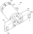
Fig. 17 is a perspective view of a bare chip handling tool for flip chip (flip chip) for explaining an embodiment.
Fig. 18 is a perspective view of a bare chip handling tool for flip chip for illustrating an embodiment.
Fig. 19 is a perspective view of a bare chip handling tool for flip chip for explaining an embodiment.
Fig. 20 is a perspective view of a bare chip handling tool for flip chip for illustrating an embodiment. Description of the reference numerals
1: chip mounting device
10: wafer stage
11: wafer with a plurality of chips
20: pasting stand (binding stage)
21: substrate
30: wafer box
40. 40L, 40H: substrate box (magazine)
50: multifunctional manipulator
51: fixing part
52: movable part
53: tool connecting part
54: force sensor
55: vision camera (vision camera)
60: manipulator for jacking
70: wafer handling tool
80: substrate handling tool
90: bare chip handling tool
Detailed Description
A part of a manufacturing process of a semiconductor device includes a step of mounting a semiconductor chip (hereinafter, referred to simply as a "bare chip") on a wiring board, a lead frame, or the like (hereinafter, referred to simply as a "board") and assembling a package (package), and a part of the step of assembling the package includes a step of dividing the bare chip from a semiconductor wafer (hereinafter, referred to simply as a "wafer") and a mounting step of mounting the divided bare chip on the board. The manufacturing apparatus used in the mounting process is a chip mounter such as a chip mounter or a flip chip mounter.
The die mounter is a device for mounting a bare chip on a substrate or a mounted (mounted and bonded) bare chip using solder, gold plating, or resin as a bonding material. In a mounting apparatus for mounting a bare chip on a surface of a substrate, for example, the following operations (operations) are repeated: a bare chip is sucked from a wafer and picked up by using a suction nozzle called a collet (collet), and the bare chip is transferred onto a substrate, and is mounted by applying a pressing force and heating a bonding material. The collet is a holder having a suction hole and sucking and holding the bare chip by sucking air, and has a size similar to that of the bare chip.
In the die bonding apparatus according to the embodiment, a wafer cassette for housing a wafer ring and a substrate cassette for housing a substrate are disposed on a front surface side, a wafer stage is fixedly disposed on a rear surface side, and a bonding stage is disposed between the wafer cassette and the wafer stage. The wafer, the substrate, and the bare chip are carried by one robot, and the carrying directions in the horizontal direction are the same. This enables the device to be miniaturized.
Hereinafter, embodiments will be described with reference to the drawings. However, in the following description, the same components are denoted by the same reference numerals, and redundant description thereof may be omitted. In addition, although the drawings schematically show the width, thickness, shape, and the like of each part as compared with the actual form in order to clarify the description, the drawings are merely examples and do not limit the explanation of the present invention.
Examples
The die bonding apparatus according to the embodiment will be described with reference to fig. 1. Fig. 1 is a perspective view showing a structure of a chip mounter according to an embodiment. Fig. 1 shows a plurality of states of a multifunction manipulator described later.
The die bonding apparatus 1 of the embodiment has an apparatus body 2 having a front surface with a width W, a depth D, and a height H. The apparatus main body 2 has a base plate base 3, a top base 4, and an intermediate base 5 disposed therebetween. A jack-up robot 60 is fixed to the base plate 3, and a multifunction robot 50 is fixed to the lower part of the top base 4. On the intermediate base 5, a wafer stage 10 is fixed on the back surface side, and a mounting stage 20 is fixed on the front surface side adjacent to the wafer stage 10. A hole is opened in the intermediate base 5 below the wafer stage 10. A wafer cassette 30 is disposed on the front surface side of the mounting table 20 and above the intermediate base 5, the wafer cassette 30 accommodating the wafer ring 14 holding the wafer 11, and a substrate cassette 40 accommodating the substrate 21 is disposed above the wafer cassette 30. For example, when the wafer 11 has a diameter of at most 300mm (12 inches) and the substrate 21 has a size of at most 310 × 310mm, the size of the apparatus main body 2 is preferably 450mm, 1600mm, or 1500 mm.
Next, a detailed structure of the wafer stage will be described with reference to fig. 3. Fig. 3 is a sectional view showing a structure of a wafer stage of the embodiment. A Die Attach Film (DAF)18 is bonded to the back surface of the wafer 11, and a dicing tape (dicing tape)16 is bonded to the back surface of the die attach film 18. The edge of the dicing tape 16 is bonded to the wafer ring 14, and sandwiched and fixed in the expansion portion (expander) 15. The expansion portion 15 is constituted by a cylinder (cylinder) or the like, and the inverted L-shaped portion is rotatable and movable up and down. That is, the wafer stage 10 includes: an extension portion 15 that presses down the wafer ring 14; and a supporting ring 17 that horizontally positions the dicing tape 16 held by the wafer ring 14 and having the plurality of bare chips D (wafer 11) bonded thereto. As the die D is thinned, the adhesive for die bonding is changed from a liquid state to a film state, and a film-like adhesive material called an adhesive sheet film 18 is bonded between the wafer 11 and the dicing tape 16. In the wafer 11 having the adhesive sheet film 18, dicing is performed on the wafer 11 and the adhesive sheet film 18. Further, the dicing tape 16 and the adhesive sheet film 18 may be integrated.
Next, the structure of the multifunction robot 50 will be described with reference to fig. 4. Fig. 4 is a perspective view showing the structure of the multifunction robot of the embodiment. The multifunction robot 50 of the embodiment is a vertical-type multi-degree-of-freedom multi-joint robot. The multifunction robot 50 includes a fixed portion 51, a movable portion 52, a tool changer 53, a force sensor 54, and a vision camera (vision camera) 55. The tool connection portion 53 is of a male type (male type) and is connected to a female type (female type) connection portion of various tools to be described later. As various tools, there are a wafer handling tool 70, a substrate handling tool 80, a bare chip handling tool 90, and the like. The storage sections of the various tools are disposed at positions that do not hinder wafer transfer, substrate transfer, and pick and place (place) within the operating range of the multifunction robot 50.
Next, the wafer handling tool 70 will be described with reference to fig. 5 and 6. Fig. 5 is a perspective view showing the structure of the wafer handling tool according to the embodiment. Fig. 6 is a perspective view showing a state in which the wafer handling tool is attached to the multifunction robot of the embodiment.
As shown in fig. 5, the wafer handling tool 70 has a wafer chucking part 71 and a connecting part 72. The wafer chuck 71 holds the wafer ring 14. The connection portion 72 is of a female type (female type) and engages with the tool connection portion 53 of the multifunction robot 50. As shown in fig. 6, a wafer handling tool 70 mounted at the front end of the multifunction robot 50 grips the wafer ring 14 and moves it in and out with respect to the wafer cassette 30.
Next, the substrate handling tool 80 will be described with reference to fig. 7 and 8. Fig. 7 is a perspective view showing the structure of the substrate handling tool according to the embodiment. Fig. 8 is a perspective view of the multi-function robot according to the embodiment in a state where the substrate handling tool is attached.
As shown in fig. 7, the substrate handling tool 80 includes a mounting portion 81, a support portion 82, and a connecting portion 83. The mounting portion 81 is substantially the same size as the substrate 31, is flat, and is a portion on which the substrate 31 is mounted. The support portion 82 has a columnar shape and is connected to the mounting portion 81 and the connecting portion 83. The connection portion 83 is of a female type (female type) and engages with the tool connection portion 53 of the multifunction robot 50. As shown in fig. 8, the substrate handling tool 80 attached to the front end of the multi-function robot 50 carries the substrate 21 and places it on the mounting table 20 or removes it from the mounting table 20.
Next, the bare chip handling tool 90 will be described with reference to fig. 9 and 10. Fig. 9 is a perspective view showing the structure of the bare chip handling tool according to the embodiment. Fig. 10 is a perspective view of a state in which a bare chip handling tool is attached to the multifunction robot of the embodiment.
As shown in fig. 9, the bare chip handling tool 90 includes a head 91 and a connection portion 92. A collet 93 is attached to the front end of the head 91 to suck the bare chip D. The connection portion 92 is of a female type (female type) and engages with the tool connection portion 53 of the multifunction robot 50. As shown in fig. 10, the bare chip handling tool 90 is mounted to the front end of the multifunction robot 50.
Next, the structure of the jack-up robot 60 will be described with reference to fig. 11. Fig. 11 is a perspective view showing the structure of the jack-up robot according to the embodiment. The jack-up robot 60 of the embodiment is a vertical multi-degree-of-freedom multi-joint robot. The jack-up robot 60 includes a fixed part 61, a movable part 62, and a jack-up tool part 63. The jack-up tool 63 can be replaced according to the type or product.
Next, the operation of the chip mounter 1 will be described with reference to fig. 12A, 12B, and 13 to 16. Fig. 12A and 12B are flowcharts for explaining the operation of the chip mounter according to the embodiment. Fig. 13 is a perspective view for explaining an operation of the die bonding apparatus according to the embodiment when a wafer is carried. Fig. 14 is a perspective view for explaining an operation of the chip mounter according to the embodiment when the substrate is transported. Fig. 15 is a perspective view for explaining the operation of the chip mounter in picking up and mounting according to the embodiment. Fig. 16 is a perspective view for explaining a picking operation of the chip mounter according to the embodiment.
The die bonding apparatus 1 includes a control device, not shown, including a cpu (central Processor unit), a memory for storing a control program, a memory for storing data, a control bus, and the like, not shown, and controls the respective elements constituting the die bonding apparatus 1, such as the multifunction robot 50 and the jack-up robot 60.
The operations of the chip mounter 1 are divided into initialization (step S1), wafer conveyance (step S2), substrate conveyance (step S3), and pick and place (step S3).
Step S1: the controller initializes (initialize) the elements constituting the chip mounter 1, such as the multifunction robot 50 and the lift robot 60.
The wafer transfer in step S2 performs the following operations.
Step S21: the control unit mounts a wafer handling tool 70 (a tool for wafer replacement) on the multifunction robot 50.
Step S22: the controller confirms the presence or absence of the wafer cassette 30 (confirms the presence or absence of the wafer cassette) by using the vision camera 55 of the multifunction robot 50.
Step S23: the controller confirms the presence or absence of the wafer 11 (wafer ring 14) using the vision camera 55 of the multifunction robot 50 (confirms the presence or absence of the wafer).
Step S24: the controller takes out the wafer ring 14 holding the wafer 11 from the wafer cassette 30 and carries it onto the wafer stage 10 (carries the wafer) as shown in fig. 13 using the wafer handling tool 70 of the multifunction robot 50.
Step S25: the controller presses the wafer ring 14 against the expanding portion 15, and elongates the dicing tape 16 held on the wafer ring 14 (expands the wafer). This enlarges the interval between the bare chips D, prevents the bare chips D from interfering with each other and coming into contact with each other, and separates the bare chips D to be easily lifted.
The substrate conveyance in step S3 performs the following operations.
Step S31: the controller removes the wafer handling tool 70 from the multi-function robot 50 and mounts the substrate handling tool 80 (substrate replacement tool).
Step S32: the controller confirms the presence or absence of the substrate cassette 40 (confirms the presence or absence of the substrate cassette) using the vision camera 55 of the multifunction robot 50.
Step S33: the control device confirms the presence or absence of the substrate 21 (confirms the presence or absence of the substrate) using the vision camera 55 of the multifunction robot 50.
Step S34: the control device takes out the substrate 21 from the substrate cassette 40L and carries it to the mounting table 20 (carries the substrate) using the substrate handling tool 80 of the multifunction robot 50, as shown in fig. 14.
The pick and place of step S4 performs the following actions.
Step S41: the controller removes the substrate handling tool 80 from the multifunction robot 50 and mounts the bare chip handling tool 90 (replaces the bare chip tool).
Step S42: the control device corrects the position of the die handling tool 90 (corrects the die position).
Step S43: the control device recognizes an alignment mark (recognition wafer alignment mark) of the wafer 11 using the vision camera 55 of the multifunction robot 50.
Step S44: the control device recognizes the alignment mark of the substrate 21 (recognizes the substrate alignment mark) using the vision camera 55 of the multifunction robot 50.
Step S45: as shown in fig. 15 and 16, the control device raises the raising tool portion 63 of the raising robot 60 from below the bare chip D, lowers the collet 93 attached to the bare chip handling tool 90 of the multifunction robot 50 from above the bare chip D, and picks up the bare chip D. In this case, the inclination may be set for the picking and the jack-up action. The multifunction robot 50 and the jack-up robot 60 can perform the operation with 6 degrees of freedom of XYZ axes/α β θ axes, and the collet 93 can perform the flexible operation of lifting the bare chip D by hand. The lifter 63 may have a function of sucking and holding the dicing tape 16, and may perform not only the lifting operation but also an operation of pulling down the tape by hand. By operating both the collet 93 and the jack-up tool portion 63, complicated and reliable picking-up can be achieved.
Step S46: the control device corrects the position of the bare chip D picked up based on the wafer alignment mark recognized in step S43, the substrate alignment mark recognized in step S44, and the force sensor 54.
Step S47: the control device inspects the appearance of the die D (inspects the die appearance) using a vision camera (not shown) located below the picked die D.
Step S48: the control means mounts the picked bare chip D on the substrate 21 or on the already mounted bare chip.
Step S49: the control device determines whether there is no substrate to be mounted on the mounting table 20. If the determination result is yes, the process proceeds to step S4B, and if the determination result is no, the process proceeds to step S4A.
Step S4A: the control means determines whether there is no bare chip to be picked up on the wafer 11. If the determination result is yes, the process proceeds to step S4C, and if the determination result is no, the process proceeds to step S45.
Step S4B: the control device replaces the substrate. First, the control device removes the bare chip handling tool 90 from the multifunctional robot 50 and mounts the substrate handling tool 80. Next, the control device removes the substrate 21 from the mounting table 20 using the substrate handling tool 80 of the multifunction robot 50, and conveys it to a substrate cassette 40H different from the substrate cassette 40L mounted before mounting. Next, the control device takes out the next substrate from the substrate cassette 40L and carries it to the mounting table 20 using the substrate handling tool 80 of the multifunction robot 50. Thereafter, the process returns to step S41.
Step S4C: the control device replaces the wafer. First, the control device removes the bare chip handling tool 90 from the multifunctional robot 50 and mounts the wafer handling tool 70. Next, the controller takes out the wafer ring 14 from the wafer stage 10 and conveys it to the wafer cassette 30 using the wafer handling tool 70 of the multifunction robot 50. Next, the controller takes out the next wafer ring from the wafer cassette 30 and carries it to the wafer stage 10 using the wafer handling tool 70 of the multifunction robot 50. The control means presses the wafer ring 14 through the expanding portion 15 to elongate the dicing tape 16 held on the wafer ring 14. Thereafter, the process returns to step S41.
Next, a bare chip handling tool in the case where the chip mounter 1 is used as a flip chip mounter will be described with reference to fig. 17 to 20. Fig. 17 is a perspective view showing a 1 st state of the bare chip handling tool for flip chip according to the embodiment. Fig. 18 is a perspective view showing a 2 nd state of the bare chip handling tool for flip chip according to the embodiment. Fig. 19 is a perspective view showing a 3 rd state of the bare chip handling tool for flip chip according to the embodiment. Fig. 20 is a perspective view showing a 4 th state of the bare chip handling tool for flip chip according to the embodiment.
As shown in fig. 17, the die manipulator 100 for flip chip mounter includes a pick-up head 101, a flip-chip head 102, a base portion 103, and a connecting portion 104. The pick-up head 101 and the flip-chip head 102 have respective chucks 105 and 106 for sucking the bare chip D. The pick-up head 101 and the flip-chip head 102 are movable.
Fig. 17 shows a state in which the pickup head 101 and the flip head 102 are opened (1 st state). In the 1 st state, the pick-up head 101 picks up the bare chip D by the collet 105.
Fig. 18 is a state where the pickup head 101 is opened, and is a state where the flip head 102 is closed (2 nd state). The pickup head 101 may be closed and the flip head 102 may be opened. The 2 nd state is a state following the 1 st state.
Fig. 19 shows a state where the pickup head 101 and the flip head 102 are closed (state 3). In the 3 rd state, the bare chip D is sucked by the collet 106 of the flip-chip head 102, and the suction of the bare chip D by the collet 105 of the pick-up head 101 is released. The 3 rd state is a state following the 2 nd state.
Fig. 20 shows a state in which the pickup head 101 and the flip head 102 are opened (4 th state). In the 4 th state, the bare chip D is reversed and transferred from the pick-up head 101 to the flip-chip head 102, and the flip-chip head 102 places (mounts) the bare chip D sucked by the collet 106 on a substrate or the like. The 4 th state is a state following the 3 rd state.
The die bonding apparatus of the embodiment exerts the following effects.
Since the multi-degree-of-freedom multi-joint mechanism is used for the robot, the robot has a large movable region and can perform an operation of changing the posture, and can be used for various operations such as discharging of wafers and storing of substrate cassettes. This can reduce the number of mechanism parts. Further, a simple layout structure in which the wafer cassette/substrate cassette, the mounting table, and the wafer table are arranged in one direction can be realized, and the device can be reduced in weight and size.
Further, since the taking in and taking out of the wafer (wafer cassette) and the substrate (substrate cassette) are performed only from the front surface of the apparatus and the width of the apparatus is narrowed, by arranging a plurality of apparatuses in parallel and operating the plurality of apparatuses in parallel, it is possible to suppress an increase in the area occupied by the apparatus and improve the throughput.
Further, since the multi-degree-of-freedom multi-joint mechanism is used, the robot can be conveyed in cooperation with each of the pick-up point and the placing point, and adjustment is facilitated.
Further, a multi-degree-of-freedom multi-joint mechanism is used as a mechanism for driving the pickup head and the jack-up mechanism, and the mechanism for driving the pickup and the jack-up are operated in cooperation with each other, whereby the pickup/jack-up operation can be operated with an inclination. When the bare chip bonded to the dicing tape is peeled off, the bare chip can be operated while changing the relative angle, and the operation that cannot be realized by the mechanism of the orthogonal coordinate system is achieved, so that the pickup performance can be improved.
In addition, the die mounter can be changed to a flip chip mounter by replacing the bare chip handling tool.
The invention made by the inventors of the present application has been described above based on the embodiments, but the present invention is not limited to the above embodiments, and it goes without saying that various modifications are possible.
In the embodiment, the case where the substrate cassette is disposed above the wafer cassette and the mounting table and the wafer stage are disposed in one direction is described, but the substrate cassette may be disposed near the wafer cassette. The housing portions for various tools may be disposed in the vertical direction of the wafer cassette or the substrate cassette. Further, the multifunction robot may be arranged at the center and a wafer cassette, a substrate cassette, a mounting table, and a wafer table may be arranged at the periphery thereof in a cluster tool (cluster tool) manner.
In the embodiment, the wafer ring, the substrate, and the bare chip are transported by one multi-function robot, but may be transported by a plurality of robots.
In the embodiment, the case of using the vertical type multiple degree of freedom multiple joint mechanism is described, but the multiple degree of freedom multiple joint mechanism may be a horizontal type or a parallel connection type (parallel link type).
The chip mounter is explained in the embodiments, but it can also be used as a die sorter (die sorter) by placing the tray on the mounting table.
Claims (9)
1. A chip mounting device is provided with:
a device main body;
a wafer cassette for accommodating a wafer ring for holding a wafer;
a substrate cassette for housing a substrate;
a wafer stage for holding the wafer ring;
a mounting table on which a substrate is mounted to mount a bare chip picked up from the wafer;
a first robot having a multi-degree-of-freedom multi-joint mechanism for carrying the wafer ring, the substrate, and the bare chip; and
a 2 nd robot disposed below the wafer stage and picking up the bare chip in cooperation with the 1 st robot,
the multi-degree-of-freedom multi-joint mechanism of the 1 st manipulator is a 6-degree-of-freedom multi-joint mechanism having XYZ axes and alpha beta theta axes,
the 2 nd manipulator has a 6-degree-of-freedom multi-joint mechanism having XYZ and α β θ axes.
2. The chip mounting apparatus according to claim 1,
the 1 st manipulator is a vertical multi-degree-of-freedom multi-joint manipulator fixed to the top of the device body.
3. The chip mounting apparatus according to claim 1,
the 1 st robot has a vision camera at its tip.
4. The chip mounting apparatus according to claim 1,
the wafer stage includes: an expanding portion that presses down the wafer ring; and a support ring that horizontally positions a dicing tape held to the wafer ring and to which the wafer is bonded.
5. The chip mounting apparatus according to claim 1,
the 2 nd robot includes a tool for lifting up the bare chip at a tip thereof.
6. The chip mounting apparatus according to claim 5,
the tool can be replaced.
7. The chip mounting apparatus according to claim 5,
the 2 nd manipulator is a vertical multi-degree-of-freedom multi-joint manipulator fixed on a bottom plate of the device main body.
8. A method for manufacturing a semiconductor device, comprising the steps of:
(a) a step of preparing a die bonding device including a device main body, a wafer cassette for accommodating a wafer ring for holding a dicing tape bonded to a wafer, a 1 st substrate cassette and a 2 nd substrate cassette for accommodating substrates, a wafer stage for fixing the wafer ring, a mounting stage for mounting a substrate for mounting a bare chip picked up from the wafer, a 1 st robot having a 6-degree-of-freedom multi-joint mechanism having an XYZ axis and an α β θ axis, and a 2 nd robot having a 6-degree-of-freedom multi-joint mechanism having an XYZ axis and an α β θ axis;
(b) a step of transferring the wafer ring from the wafer cassette to the wafer stage by the 1 st robot;
(c) a step of conveying the substrate from the 1 st substrate cassette to the mounting table by the 1 st robot;
(d) picking up the bare chip by the 1 st robot and the 2 nd robot in cooperation;
(e) a step of conveying the picked bare chip by the 1 st manipulator and attaching the bare chip to the substrate on the mounting table; and
(f) and a step of transferring the substrate mounted with the bare chip to the 2 nd substrate cassette by the 1 st robot.
9. The method for manufacturing a semiconductor device according to claim 8,
in the step (d), the wafer handling tool at the tip of the 1 st robot is set at a predetermined angle to be brought into contact with the bare chip, and the tip of the 2 nd robot is set at a predetermined angle to be brought into contact with the dicing tape to pick up the bare chip.
Priority Applications (1)
| Application Number | Priority Date | Filing Date | Title |
|---|---|---|---|
| CN202110446716.4A CN113192867B (en) | 2016-03-11 | 2016-11-18 | Chip mounting apparatus and method for manufacturing semiconductor device |
Applications Claiming Priority (2)
| Application Number | Priority Date | Filing Date | Title |
|---|---|---|---|
| JP2016-048988 | 2016-03-11 | ||
| JP2016048988A JP6705668B2 (en) | 2016-03-11 | 2016-03-11 | Die bonding apparatus and semiconductor device manufacturing method |
Related Child Applications (1)
| Application Number | Title | Priority Date | Filing Date |
|---|---|---|---|
| CN202110446716.4A Division CN113192867B (en) | 2016-03-11 | 2016-11-18 | Chip mounting apparatus and method for manufacturing semiconductor device |
Publications (2)
| Publication Number | Publication Date |
|---|---|
| CN107180772A CN107180772A (en) | 2017-09-19 |
| CN107180772B true CN107180772B (en) | 2021-04-30 |
Family
ID=59830188
Family Applications (2)
| Application Number | Title | Priority Date | Filing Date |
|---|---|---|---|
| CN202110446716.4A Active CN113192867B (en) | 2016-03-11 | 2016-11-18 | Chip mounting apparatus and method for manufacturing semiconductor device |
| CN201611028985.4A Active CN107180772B (en) | 2016-03-11 | 2016-11-18 | Chip mounting device and method for manufacturing semiconductor device |
Family Applications Before (1)
| Application Number | Title | Priority Date | Filing Date |
|---|---|---|---|
| CN202110446716.4A Active CN113192867B (en) | 2016-03-11 | 2016-11-18 | Chip mounting apparatus and method for manufacturing semiconductor device |
Country Status (4)
| Country | Link |
|---|---|
| JP (1) | JP6705668B2 (en) |
| KR (2) | KR101835232B1 (en) |
| CN (2) | CN113192867B (en) |
| TW (1) | TWI615905B (en) |
Families Citing this family (10)
| Publication number | Priority date | Publication date | Assignee | Title |
|---|---|---|---|---|
| JP7018338B2 (en) * | 2018-03-19 | 2022-02-10 | ファスフォードテクノロジ株式会社 | Manufacturing method of die bonding equipment and semiconductor equipment |
| JP7102271B2 (en) * | 2018-07-17 | 2022-07-19 | ファスフォードテクノロジ株式会社 | Semiconductor manufacturing equipment and manufacturing method of semiconductor equipment |
| KR102113118B1 (en) * | 2018-11-21 | 2020-05-20 | 제너셈(주) | Package unloading apparatus |
| KR20200065175A (en) | 2018-11-29 | 2020-06-09 | 삼성디스플레이 주식회사 | Substrate transfering system and method of transfering the substrate |
| JP7146352B2 (en) * | 2018-12-10 | 2022-10-04 | 株式会社ディスコ | test equipment |
| JP7184620B2 (en) * | 2018-12-11 | 2022-12-06 | 株式会社ディスコ | cutting equipment |
| KR20200119971A (en) | 2019-04-11 | 2020-10-21 | 주식회사 지와이엘테크놀로지 | Semiconductor bonding device and the method therefor |
| TWI734434B (en) * | 2019-04-11 | 2021-07-21 | 日商新川股份有限公司 | Joining device |
| JP6880158B1 (en) * | 2019-11-29 | 2021-06-02 | キヤノンマシナリー株式会社 | Work transfer device, work transfer method, transfer body manufacturing method, semiconductor device manufacturing method, and die bonder |
| KR102434404B1 (en) * | 2022-04-05 | 2022-08-18 | 홍문복 | optical bonding process equipment for assembling car cluster and method using it |
Citations (4)
| Publication number | Priority date | Publication date | Assignee | Title |
|---|---|---|---|---|
| TW200929423A (en) * | 2007-08-15 | 2009-07-01 | Applied Materials Inc | Pulsed laser anneal system architecture |
| KR20100055809A (en) * | 2008-11-18 | 2010-05-27 | 세메스 주식회사 | Apparatus for processing a substrate |
| TW201312681A (en) * | 2011-06-03 | 2013-03-16 | Orion Systems Integration Pte Ltd | Method and systems for semiconductor chip pick & transfer and bonding |
| TW201521138A (en) * | 2013-08-09 | 2015-06-01 | Hitachi High Tech Instr Co Ltd | Collet and die bonder |
Family Cites Families (32)
| Publication number | Priority date | Publication date | Assignee | Title |
|---|---|---|---|---|
| JP3030400B2 (en) * | 1994-02-24 | 2000-04-10 | 株式会社三井ハイテック | Automatic die bonding method |
| JPH08306764A (en) * | 1995-05-02 | 1996-11-22 | Tokyo Electron Ltd | Method and machine for mounting semiconductor device |
| JPH10277981A (en) * | 1997-04-07 | 1998-10-20 | Nittetsu Semiconductor Kk | Robot hand |
| JPH10335410A (en) * | 1997-05-29 | 1998-12-18 | Sony Corp | Wafer carrier and method of aligning wafer |
| JP3938436B2 (en) * | 1998-06-05 | 2007-06-27 | 大日本スクリーン製造株式会社 | Substrate transfer apparatus and substrate processing apparatus using the same |
| KR100278603B1 (en) * | 1998-09-30 | 2001-01-15 | 윤종용 | Die bonding equipment and die bonding method for microgap ball grid array packages |
| JP4234300B2 (en) * | 2000-05-09 | 2009-03-04 | ヤマハ発動機株式会社 | Chip transfer device |
| JP2002076094A (en) * | 2000-08-31 | 2002-03-15 | Daikin Ind Ltd | Board carrying apparatus |
| JP5051948B2 (en) * | 2001-05-30 | 2012-10-17 | 株式会社ダイヘン | Cassette transport method and cassette transport system |
| KR100407568B1 (en) * | 2001-06-01 | 2003-12-01 | 삼성전자주식회사 | Apparatus for processing semiconductor having foup index inside apparatus establishing area |
| EP1446828A2 (en) * | 2001-11-13 | 2004-08-18 | Fsi International, Inc. | Reduced footprint tool for automated processing of substrates |
| JP2004055697A (en) * | 2002-07-17 | 2004-02-19 | Ace:Kk | Apparatus and method for transferring and conveying substrate |
| TW586996B (en) * | 2003-07-04 | 2004-05-11 | Advanced Semiconductor Eng | Wafer transport robot arm |
| JP4096850B2 (en) * | 2003-09-18 | 2008-06-04 | 松下電器産業株式会社 | Object conveying apparatus and object conveying method |
| JP2006073834A (en) * | 2004-09-02 | 2006-03-16 | Dainippon Screen Mfg Co Ltd | Substrate transport device and substrate treatment equipment employing it |
| JP4602750B2 (en) * | 2004-12-13 | 2010-12-22 | 東京エレクトロン株式会社 | Processing apparatus and processing method |
| JP4767641B2 (en) * | 2005-09-27 | 2011-09-07 | 大日本スクリーン製造株式会社 | Substrate processing apparatus and substrate transfer method |
| JP4890873B2 (en) * | 2006-02-06 | 2012-03-07 | リンテック株式会社 | Sheet pasting device |
| JP2006191144A (en) * | 2006-03-13 | 2006-07-20 | Toshiba Corp | Pickup device and pickup method |
| JP4585496B2 (en) | 2006-08-25 | 2010-11-24 | 芝浦メカトロニクス株式会社 | Semiconductor chip mounting equipment |
| US9050634B2 (en) * | 2007-02-15 | 2015-06-09 | SCREEN Holdings Co., Ltd. | Substrate processing apparatus |
| CN101540291A (en) * | 2009-03-23 | 2009-09-23 | 常州新区爱立德电子有限公司 | Automatic sorting machine for semiconductor chip |
| KR20120123920A (en) * | 2011-05-02 | 2012-11-12 | 나노에프에이 주식회사 | Semiconductor manufacturing apparatus having vision system for real-time monitoring wafer transfer unit |
| JP2013049113A (en) * | 2011-08-31 | 2013-03-14 | Yaskawa Electric Corp | Robot arm structure, and robot |
| KR20130026805A (en) | 2011-09-06 | 2013-03-14 | 삼성전자주식회사 | Wire bonding system for semiconductor package |
| JP5941701B2 (en) * | 2012-02-23 | 2016-06-29 | ファスフォードテクノロジ株式会社 | Die bonder |
| KR20140003281A (en) * | 2012-06-29 | 2014-01-09 | 한미반도체 주식회사 | Semionductor chip bonding system |
| JP6111065B2 (en) * | 2012-12-28 | 2017-04-05 | 川崎重工業株式会社 | Automatic teaching system and teaching method |
| JPWO2014157134A1 (en) * | 2013-03-28 | 2017-02-16 | 東レエンジニアリング株式会社 | Mounting method and mounting apparatus |
| JP6118620B2 (en) * | 2013-04-03 | 2017-04-19 | ヤマハ発動機株式会社 | Component mounting equipment |
| CN203491228U (en) * | 2013-10-12 | 2014-03-19 | 四川蓝彩电子科技有限公司 | Wafer assembling system |
| KR101483987B1 (en) * | 2014-06-16 | 2015-01-20 | 주식회사 로보스타 | Transfer robot having variable hand of four robot arms |
-
2016
- 2016-03-11 JP JP2016048988A patent/JP6705668B2/en active Active
- 2016-11-04 TW TW105135963A patent/TWI615905B/en active
- 2016-11-18 CN CN202110446716.4A patent/CN113192867B/en active Active
- 2016-11-18 CN CN201611028985.4A patent/CN107180772B/en active Active
- 2016-11-18 KR KR1020160153978A patent/KR101835232B1/en active IP Right Grant
-
2018
- 2018-02-26 KR KR1020180022825A patent/KR101990242B1/en active IP Right Grant
Patent Citations (4)
| Publication number | Priority date | Publication date | Assignee | Title |
|---|---|---|---|---|
| TW200929423A (en) * | 2007-08-15 | 2009-07-01 | Applied Materials Inc | Pulsed laser anneal system architecture |
| KR20100055809A (en) * | 2008-11-18 | 2010-05-27 | 세메스 주식회사 | Apparatus for processing a substrate |
| TW201312681A (en) * | 2011-06-03 | 2013-03-16 | Orion Systems Integration Pte Ltd | Method and systems for semiconductor chip pick & transfer and bonding |
| TW201521138A (en) * | 2013-08-09 | 2015-06-01 | Hitachi High Tech Instr Co Ltd | Collet and die bonder |
Also Published As
| Publication number | Publication date |
|---|---|
| JP6705668B2 (en) | 2020-06-03 |
| CN107180772A (en) | 2017-09-19 |
| TW201732961A (en) | 2017-09-16 |
| CN113192867B (en) | 2024-01-23 |
| KR20170106175A (en) | 2017-09-20 |
| CN113192867A (en) | 2021-07-30 |
| KR20180028057A (en) | 2018-03-15 |
| JP2017163121A (en) | 2017-09-14 |
| KR101835232B1 (en) | 2018-03-06 |
| TWI615905B (en) | 2018-02-21 |
| KR101990242B1 (en) | 2019-09-24 |
Similar Documents
| Publication | Publication Date | Title |
|---|---|---|
| CN107180772B (en) | Chip mounting device and method for manufacturing semiconductor device | |
| CN108987305B (en) | Semiconductor manufacturing apparatus and method for manufacturing semiconductor device | |
| CN107622955B (en) | Semiconductor manufacturing apparatus and method for manufacturing semiconductor device | |
| CN108346585B (en) | Semiconductor manufacturing apparatus and method for manufacturing semiconductor device | |
| JP6086763B2 (en) | Collet cleaning method and die bonder using the same | |
| CN107492510B (en) | Semiconductor manufacturing apparatus and method for manufacturing semiconductor device | |
| US8857486B2 (en) | Flip arm module for a bonding apparatus incorporating changeable collet tools | |
| WO2010032427A1 (en) | Component mounting apparatus and component mounting method | |
| CN109524313B (en) | Semiconductor manufacturing apparatus, semiconductor device manufacturing method, and collet | |
| CN104347435A (en) | An adsorption collet chuck and a chip adapter | |
| JP6941513B2 (en) | Semiconductor manufacturing equipment and manufacturing method of semiconductor equipment | |
| JP2008010869A (en) | Semiconductor chip flip assembly, and semiconductor chip bonding device utilizing the same | |
| JP3861710B2 (en) | Electronic component supply device and electronic component mounting device | |
| JP6717630B2 (en) | Electronic component mounting equipment | |
| JP7205941B2 (en) | bonding equipment | |
| JP2001320195A (en) | Composite mounting device | |
| JP2001319938A (en) | Chip transfer device | |
| JP4909249B2 (en) | Transfer equipment | |
| CN112530834B (en) | Chip mounting apparatus, peeling unit, collet, and method for manufacturing semiconductor device | |
| JP4001106B2 (en) | Electronic component pickup apparatus and electronic component pickup method | |
| JP2020074483A (en) | Electronic component implementation apparatus | |
| JP2022183724A (en) | Pickup method, and, pickup device | |
| JPH11297718A (en) | Die pickup method and semiconductor manufacturing device using the same |
Legal Events
| Date | Code | Title | Description |
|---|---|---|---|
| PB01 | Publication | ||
| PB01 | Publication | ||
| SE01 | Entry into force of request for substantive examination | ||
| SE01 | Entry into force of request for substantive examination | ||
| GR01 | Patent grant | ||
| GR01 | Patent grant |