CN1034702C - Microelectronic device package containing a liquid and method - Google Patents
Microelectronic device package containing a liquid and method Download PDFInfo
- Publication number
- CN1034702C CN1034702C CN94115277A CN94115277A CN1034702C CN 1034702 C CN1034702 C CN 1034702C CN 94115277 A CN94115277 A CN 94115277A CN 94115277 A CN94115277 A CN 94115277A CN 1034702 C CN1034702 C CN 1034702C
- Authority
- CN
- China
- Prior art keywords
- liquid
- lid
- base
- shell
- temperature
- Prior art date
- Legal status (The legal status is an assumption and is not a legal conclusion. Google has not performed a legal analysis and makes no representation as to the accuracy of the status listed.)
- Expired - Fee Related
Links
Images


Classifications
-
- H—ELECTRICITY
- H01—ELECTRIC ELEMENTS
- H01L—SEMICONDUCTOR DEVICES NOT COVERED BY CLASS H10
- H01L23/00—Details of semiconductor or other solid state devices
- H01L23/02—Containers; Seals
-
- H—ELECTRICITY
- H01—ELECTRIC ELEMENTS
- H01L—SEMICONDUCTOR DEVICES NOT COVERED BY CLASS H10
- H01L23/00—Details of semiconductor or other solid state devices
- H01L23/16—Fillings or auxiliary members in containers or encapsulations, e.g. centering rings
- H01L23/18—Fillings characterised by the material, its physical or chemical properties, or its arrangement within the complete device
- H01L23/22—Fillings characterised by the material, its physical or chemical properties, or its arrangement within the complete device liquid at the normal operating temperature of the device
-
- H—ELECTRICITY
- H01—ELECTRIC ELEMENTS
- H01L—SEMICONDUCTOR DEVICES NOT COVERED BY CLASS H10
- H01L21/00—Processes or apparatus adapted for the manufacture or treatment of semiconductor or solid state devices or of parts thereof
- H01L21/02—Manufacture or treatment of semiconductor devices or of parts thereof
- H01L21/04—Manufacture or treatment of semiconductor devices or of parts thereof the devices having at least one potential-jump barrier or surface barrier, e.g. PN junction, depletion layer or carrier concentration layer
- H01L21/50—Assembly of semiconductor devices using processes or apparatus not provided for in a single one of the subgroups H01L21/06 - H01L21/326, e.g. sealing of a cap to a base of a container
- H01L21/54—Providing fillings in containers, e.g. gas fillings
-
- H—ELECTRICITY
- H01—ELECTRIC ELEMENTS
- H01L—SEMICONDUCTOR DEVICES NOT COVERED BY CLASS H10
- H01L23/00—Details of semiconductor or other solid state devices
- H01L23/34—Arrangements for cooling, heating, ventilating or temperature compensation ; Temperature sensing arrangements
- H01L23/42—Fillings or auxiliary members in containers or encapsulations selected or arranged to facilitate heating or cooling
-
- H—ELECTRICITY
- H01—ELECTRIC ELEMENTS
- H01L—SEMICONDUCTOR DEVICES NOT COVERED BY CLASS H10
- H01L2924/00—Indexing scheme for arrangements or methods for connecting or disconnecting semiconductor or solid-state bodies as covered by H01L24/00
- H01L2924/0001—Technical content checked by a classifier
- H01L2924/0002—Not covered by any one of groups H01L24/00, H01L24/00 and H01L2224/00
-
- Y—GENERAL TAGGING OF NEW TECHNOLOGICAL DEVELOPMENTS; GENERAL TAGGING OF CROSS-SECTIONAL TECHNOLOGIES SPANNING OVER SEVERAL SECTIONS OF THE IPC; TECHNICAL SUBJECTS COVERED BY FORMER USPC CROSS-REFERENCE ART COLLECTIONS [XRACs] AND DIGESTS
- Y10—TECHNICAL SUBJECTS COVERED BY FORMER USPC
- Y10T—TECHNICAL SUBJECTS COVERED BY FORMER US CLASSIFICATION
- Y10T29/00—Metal working
- Y10T29/49—Method of mechanical manufacture
- Y10T29/49002—Electrical device making
- Y10T29/49117—Conductor or circuit manufacturing
- Y10T29/49124—On flat or curved insulated base, e.g., printed circuit, etc.
- Y10T29/4913—Assembling to base an electrical component, e.g., capacitor, etc.
- Y10T29/49146—Assembling to base an electrical component, e.g., capacitor, etc. with encapsulating, e.g., potting, etc.
Landscapes
- Engineering & Computer Science (AREA)
- Physics & Mathematics (AREA)
- Condensed Matter Physics & Semiconductors (AREA)
- General Physics & Mathematics (AREA)
- Computer Hardware Design (AREA)
- Microelectronics & Electronic Packaging (AREA)
- Power Engineering (AREA)
- Manufacturing & Machinery (AREA)
- Encapsulation Of And Coatings For Semiconductor Or Solid State Devices (AREA)
- Cooling Or The Like Of Semiconductors Or Solid State Devices (AREA)
- Micromachines (AREA)
Abstract
A method for manufacturing a liquid-containing microelectronic device package. The method includes steps of providing a base including a microelectronic device and a seal area disposed peripherally about the base, providing a lid and providing a sealant disposed between the base and lid. The method also includes steps of immersing the base, sealant and lid in a liquid having a temperature above a sealant activation temperature and maintaining the base, sealant and lid in the liquid for a time sufficient to allow the liquid to enter between the base and lid and to heat and thereby activate the sealant.
Description
Present invention relates in general to the microelectronic element encapsulation field, more particularly, the present invention relates to a kind of simple, manufacturability shell that improved, that include liquid.
In recent years, have at the manufacture view of electronic equipment and more and more pay attention to being applied to the reliability of the element in these equipment and the trend of firm durability.Because several aspects, the efficiently radiates heat of power device has proposed some special problems.Generally speaking, produce heat in the structure that the upper surface of semiconductor device limits by photoetching, and be that lower surface by device realizes being connected of heat sink heat conductivity.Therefore heat is from active device area, passes through chip and then is coupled to heat sink.Increase along with the device integrated level, produce more substantial heat and be coupled by thermal conductivity and the relatively poor comparatively speaking semi-conducting material of thermal capacity at the upper surface of device, this point can determine the maximum packaging density of large scale integrated circuit and/or large-signal or power semiconductor.On chip upper surface, the device that itself not necessarily produces heat heated by proximity structure, thereby influence the electric property of these devices.
A kind of approach of getting rid of heat of having attempted with semiconductor device be placed on one through particular design, comprise in the device package and lid of liquid.Used a kind of dielectric fluid with gentle chemical property and suitable thermal property (as vapourizing temperature and curing temperature).Shell application adaptation in the prior art is in the cavity that contains liquid and be convenient to the heat exchange structure of thermal expansion and/or vacuum tube etc.These frame modes are uneconomic on cost for the application facet of many microelectronics Packaging.In addition, development up to now cavity is vacuumized and use the technology of this cavity of dielectric fluid backfill is complicated, labor-intensive, be difficult to be adapted to production in enormous quantities.Moreover, above-mentioned approach is used big cavity and the relative little liquid of volume wherein, aforesaid way can not keep liquid and lack contacting of heavy chip area under the situation of some acceleration having, unless shell is in a certain location, the application that this point can make this shell be suitable for is restricted.
In a word, the present manufacturing method and apparatus that provides semiconductor device shell full of liquid or that include liquid that needs, they also provide the manufacturability of having improved, and are suitable for range of application widely.
In brief, the invention provides a kind of new, that improved, that include liquid semiconductor device shell and manufacture method thereof.This method may further comprise the steps: a shell base is provided, and this base comprises a microelectronic component and the sealing area of a circumferential arrangement on the shell base; Provide one to be disposed at the lid above the shell base and a kind of sealant that is arranged between shell base and lid is provided.This method is further comprising the steps of: shell base, sealant and lid are immersed in the liquid of the activationary temperature that a kind of its temperature is higher than sealant, and with shell base, sealant and lid remain on experience in this liquid be enough to for one section to allow liquid enter between shell base and lid shell and the time of sealant heating with the agent of activation sealing.This method also comprises shell base, lid and sealant is shifted out from this liquid so that a microelectronic component shell good seal, that include this liquid to be provided.
Below in conjunction with description of drawings the present invention.
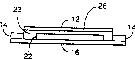
Fig. 1 shows an isometric view according to microelectronic component shell of the present invention, as to include liquid;
Fig. 2 has described a cross sectional side view of being got along the hatching 2-2 of Fig. 1;
Fig. 3 has described the cross sectional side view of second embodiment of the present invention;
Fig. 4 is the flow chart of a kind of method of a microelectronic component device shell that includes liquid according to manufacturing of the present invention.
Fig. 1 is the isometric view of saying according to microelectronic component shell 10 of the present invention, as to include liquid.Have shell 10 interior Feng Youyi the microelectronic elements (not shown in Fig. 1) that are sealed to the lid 12 on the base 16 by sealant 14.Shell 10 can be many in unique package types any of planting known in the prior art, as needle-like grid array or (PGA) shell, the dual inline type that is formed by discrete lid and base or (DIP) shell, spherical grid are listed as.Multi-chip module substrate, ceramic cartridge or the like.
Fig. 2 has described the cross sectional side view of being got along the hatching 2-2 of Fig. 1.Base 16 with electronic device 22 that the mode with chip bonding is fixed thereon also comprises the external electric interconnection line (not shown) by lead-in wire bonding As be well known in the art, scolder impact methods such as (solder bumping) and device 22 carries out electric coupling on demand.Base of being made by mono-layer oxidized aluminium (as base 16) or the multilayer base of being made by insulating material, have the electronics line can be buied from a plurality of vendor such as Kyocera international corporation as Santiago, California.
Fig. 3 is the cross sectional side view of second embodiment of expression shell 10 (Fig. 1).The embodiment class of Fig. 3 is shown in the embodiment of Fig. 2, and different is that the interior part 26 of shell is not full of by liquid, that is, it is at a bubble on the liquid 23 and in lid 12.The arrangement of this structure makes bubble part 26 can absorb the stress that liquid part 23 for example expands and produced owing to thermal response.
The lid of making by various suitable material (pottery, the metal that comprises the crown cap of drawing, plastics etc.) (as the lid 12 of Fig. 1-3), its shape and size meet the specification of buyer's needs, on request with or with thereon sealant (as having the B level epoxy resin of predetermined activation temperature or scolder) of configuration with predetermined component and melt temperature, can show that many vendor of company buy from the Kyocera state that comprises Santiago, California.
The dielectric fluid that is suitable for being included in the shell of the present invention will have following five kinds of character at least: (i) chemical property gentleness (right and wrong are reactive in the residing environment of device), liquid-solid phase transformation (or " solidifying ") temperature that (ii) has the expection operating temperature range that is lower than the semiconductor device shell, in the operating temperature range of expection, be non-electrical conductance (iii), (iv) have good thermal conductance, (v) the solution-air phase transition temperature is in the operating temperature range of expection or be higher than this scope.
In some cases, wish the heat exchange that provides by some liquid boilings that make in the shell is provided, and in other cases, the heat conduction of liquid and convection current itself just is enough to provide semiconductor device 22 needed coolings.For the former situation, be desirable to provide 26 the zone of resembling among Fig. 3 of a controlled amount, so that in the volume that provides a material of having vaporized to condense therein, on chip surface, keep one deck liquid and make the liquid 23 can thermal expansion.For the former situation, also be necessary to use a kind of sealant that under activation temperature, stands a kind of irreversible change (as chemical reaction), rather than scolder (for instance).The size of part 26 or volume will be greatly to eliminating thermal stress and little of making semiconductor device 22 topped by fluid under normal operating state.
The dielectric fluid that is fit to use according to the present invention will have two bells and whistleses at least: (vi) wetting base of not overslaugh sealant and lid are with (vii) vaporization or boiling temperature are higher than activation (as chemical change or the phase transformation) temperature of sealant.The boiling spread of suitable liquid is as follows: greater than 125 ℃ available, cater to the need greater than 100 ℃, best greater than 50 ℃.Example with liquid of condensation point temperature in usable range and boiling point comprises can (st.Paul, MN) the Fluorinert_ family low-molecular-weight of locating to buy be crossed liquid (for example, the CF that fluorination treatment is crossed from 3M company
3-((O-C
2F
4-CF
2)
n)-(O-CF
2)
m)-O-CF
3), and the Galden_ set product that can buy from the Montefluos company of Milan, ITA.
For instance, the FC-40 that 3M company produces is characterised in that: it is the mixture that 5 to 18 carbon atoms is arranged in a kind of each molecule, passed through the carbon compound of fluorination treatment, its boiling point is about 155 ℃, viscosity under the room temperature is about 2.2 centistokes(cst)s, proportion is about 1.9, and the epoxy resin of its not overslaugh such as B level epoxy resin one class is to the wetting of metal or pottery and at least than some activation temperature height of some this based epoxy resin.
Fig. 4 is the flow chart that seals a kind of method of the microelectronic component shell that includes liquid according to the present invention.Provide the method for the shell that includes liquid to begin back (block diagram 30), carry out chip by the mode consistent and fix and make the electrical interconnection line (block diagram 32) that is connected to chip with processing step thereafter.This method comprises a lid and base (this microelectronic component is connected on this base with mode electricity with physics) with a microelectronic component is placed on (block diagram 34) on the carrier together, and wherein this lid and/or base can comprise and be configured in its peripheral sealant.Under another kind of mode, the sealing agent can be a kind of preforming blank that is placed between lid and the base.Then, this carrier that will comprise lid, base and sealant is placed in the heating bath of the liquid that this shell will contain (block diagram 36).This bath (in advance) is heated to certain temperature, sealing agent or (for example stand a kind of phase transformation under this temperature, the fusing of scolder class material or thermoplastic) or (for example stand a kind of chemical change, solidifying of the thermosets of B level epoxy resin and so on), lid solidifies combination and is sealed to (block diagram 38) on the base like this.The sealing agent forms a kind of continuous seal around volume to be sealed.In the technical process of sealing, the gas that is enclosed in the shell is heated, and most of gas is substituted in most of gas in the shell from treating sealed zone to be discharged from (block diagram 38) by this liquid.Shell is shifted out from bath, so just between shell base and lid, formed sealing (block diagram 40).At this moment, the interior device of shell that includes liquid can carry out next step test (for example, the globality of check sealing, electric property or the like) with regard to being ready to (block diagram 42).
In some cases, wish to allow liquid be full of shell inside haply or fully.With lid 12 placement that turns over, base 16 is placed on together with sealant 14 on the lid 12 that turns and the sub-assembly of lid/base is immersed in this liquid, make bubble have no chance to enclose in the shell 10.Under the other situation, be expected to provide a bubble of 26 as Fig. 3.This point can be by being placed on base 16 on a kind of position of non-upset, lid 12 is placed on the top of base 16 and the mode that combinations thereof is immersed in this liquid realizes.The lid 12 that is bowl-type in shell, is the controllable air seal of volume liquid and the can that comprises a bubble thereby a kind of wherein main component is provided.Another kind of mode also is fine: can be bowl-type or dimple-shaped in the base promptly, and lid can present a kind of flat surface.
By the above, a kind of microelectronic component and manufacture method thereof that has encapsulated is provided, with respect to the method and structure in the prior art, the present invention has overcome some particular problems and certain advantage has been arranged.Technology of the present invention with a kind of simply, mode helps carrying out simultaneously removing air, joins thermal conversion liquid in the shell and the sealing shell in shell cheaply.By such arrangement, the part that microelectronic component is produced heat places directly and can contact from the liquid phase that this mode by thermal conductance, convection current and/or phase transformation (evaporation) is removed heat with a kind of, provides heat sink function with regard to direct part at circuit generation heat like this.This shell manufacturing process is very simple clear and definite, and it does not need the technological operation of special instrument, complexity, does not comprise that also application is known to operator and the harmful compound of environment, for microelectronic component provides firm durable dress envelope.
The present invention is a far reaching for the improvement of known technology, these improvement comprise make to go up summary, low manufacturing cost, rate of finished products improves and install and use in the improvement of firm durability.
Claims (10)
1. microelectronic component shell that comprises a kind of liquid, it comprises:
A base;
A microelectronic component that is equipped with on the base;
A lid that covers microelectronic component;
A kind of sealant that is configured between this base and this lid, the sealing agent is fixed on the base lid to form the liquid in cavity above-mentioned hollow between the two, sealing and a kind of cavity that is configured in sealing, it is characterized in that,
The sealing agent has an activation temperature; And the liquid that is configured in the seal chamber is the mixture that a kind of boiling point is higher than the perfluorocarbon of described activation temperature.
2. device package as claimed in claim 1 is characterized in that, described sealant is a kind of thermal activation epoxy resin with an activation temperature, and this activation temperature is characterised in that its setting temperature is lower than the boiling point of this liquid.
3. device package as claimed in claim 1 is characterized in that this base is made by aluminium oxide.
4. device package as claimed in claim 1 is characterized in that, this liquid is the mixture that a kind of boiling point is higher than 125 ℃ perfluorocarbon.
5. device package as claimed in claim 1 is characterized in that, this lid is a kind of punch forming crown cap, and it has one from the upwardly extending concave pit of base, and the air pocket that provides to have predetermined volume on liquid is provided.
6. device package as claimed in claim 1 is characterized in that, this lid is a kind of punch forming crown cap.
7. device package as claimed in claim 1 is characterized in that, this lid comprises the sealant that is configured in around this lid, the epoxy resin compound that the sealing agent is the thermal activation that is lower than described boiling point of liquid of a kind of setting temperature.
8. the method for the cavity in the shell that is filled in Feng Youyi semiconductor device is characterized in that comprising the following steps:
Heat a kind of liquid to one first temperature;
To have a lid and a base and comprise that betwixt the shell that a kind of curing temperature is lower than the sealant of this first temperature puts into this liquid so that this lid is sealed on this base; With
This shell is placed in this liquid in this cavity, contains this liquid and the sealing agent is cured.
9. a kind of method as claimed in claim 8 wherein, is placed on step in this liquid with this shell and comprises that one is stayed the step till this cavity full of liquid in this liquid with this shell.
10. a kind of method as claimed in claim 8, wherein, this shell is placed on step in this liquid comprises that one is included in step between this lid and this base with a kind of thermal activation epoxy encapsulant with an activation temperature, this activation temperature is lower than the boiling point of this liquid.
Applications Claiming Priority (2)
| Application Number | Priority Date | Filing Date | Title |
|---|---|---|---|
| US119,555 | 1993-09-13 | ||
| US08/119,555 US5413965A (en) | 1993-09-13 | 1993-09-13 | Method of making microelectronic device package containing a liquid |
Publications (2)
| Publication Number | Publication Date |
|---|---|
| CN1109219A CN1109219A (en) | 1995-09-27 |
| CN1034702C true CN1034702C (en) | 1997-04-23 |
Family
ID=22385036
Family Applications (1)
| Application Number | Title | Priority Date | Filing Date |
|---|---|---|---|
| CN94115277A Expired - Fee Related CN1034702C (en) | 1993-09-13 | 1994-09-12 | Microelectronic device package containing a liquid and method |
Country Status (6)
| Country | Link |
|---|---|
| US (2) | US5413965A (en) |
| EP (2) | EP0952610A3 (en) |
| JP (1) | JPH07106468A (en) |
| KR (1) | KR950010028A (en) |
| CN (1) | CN1034702C (en) |
| TW (1) | TW263610B (en) |
Cited By (1)
| Publication number | Priority date | Publication date | Assignee | Title |
|---|---|---|---|---|
| CN101417255B (en) * | 2007-10-24 | 2011-02-02 | 沈阳黎明航空发动机(集团)有限责任公司 | Rutile mineral aggregate processing technique |
Families Citing this family (11)
| Publication number | Priority date | Publication date | Assignee | Title |
|---|---|---|---|---|
| FR2699365B1 (en) * | 1992-12-16 | 1995-02-10 | Alcatel Telspace | System for dissipating the heat energy released by an electronic component. |
| US5716763A (en) * | 1994-12-06 | 1998-02-10 | International Business Machines Corporation | Liquid immersion heating process for substrate temperature uniformity |
| US5625227A (en) * | 1995-01-18 | 1997-04-29 | Dell Usa, L.P. | Circuit board-mounted IC package cooling apparatus |
| EP0788104B1 (en) * | 1995-08-21 | 1999-02-24 | Matsushita Electric Industrial Co., Ltd. | Multimedia optical disk capable of preserving freshness of image content for long time and its reproduction apparatus and method |
| US6144157A (en) * | 1998-05-18 | 2000-11-07 | Motorola, Inc. | Organic EL device with fluorocarbon liquid and UV epoxy layers and method |
| JP2000357766A (en) * | 1999-06-14 | 2000-12-26 | Hitachi Ltd | Sealing method of liquid refrigerant into module |
| JP2001312213A (en) | 2000-04-26 | 2001-11-09 | Internatl Business Mach Corp <Ibm> | Back light unit, liquid crystal display device, and method for manufacturing light guide plate |
| US6525420B2 (en) | 2001-01-30 | 2003-02-25 | Thermal Corp. | Semiconductor package with lid heat spreader |
| US7581585B2 (en) | 2004-10-29 | 2009-09-01 | 3M Innovative Properties Company | Variable position cooling apparatus |
| US20080266801A1 (en) * | 2007-04-30 | 2008-10-30 | Rockwell Automation Technologies, Inc. | Phase change cooled power electronic module |
| US8324719B2 (en) * | 2009-08-31 | 2012-12-04 | General Electric Company | Electronic package system |
Citations (1)
| Publication number | Priority date | Publication date | Assignee | Title |
|---|---|---|---|---|
| JPS63284837A (en) * | 1987-05-18 | 1988-11-22 | Hitachi Ltd | Cooling structure of semiconductor element |
Family Cites Families (27)
| Publication number | Priority date | Publication date | Assignee | Title |
|---|---|---|---|---|
| US4092697A (en) * | 1976-12-06 | 1978-05-30 | International Business Machines Corporation | Heat transfer mechanism for integrated circuit package |
| US4323914A (en) * | 1979-02-01 | 1982-04-06 | International Business Machines Corporation | Heat transfer structure for integrated circuit package |
| JPS56164543A (en) * | 1980-05-23 | 1981-12-17 | Hitachi Ltd | Manufacture of semiconductor device |
| JPS607739A (en) * | 1983-06-27 | 1985-01-16 | Nec Corp | Manufacture of semiconductor device |
| US4730665A (en) * | 1983-07-14 | 1988-03-15 | Technology Enterprises Company | Apparatus for cooling high-density integrated circuit packages |
| US4612978A (en) * | 1983-07-14 | 1986-09-23 | Cutchaw John M | Apparatus for cooling high-density integrated circuit packages |
| JPS6037756A (en) * | 1983-08-10 | 1985-02-27 | Mitsubishi Electric Corp | Semiconductor device |
| JPS60183743A (en) * | 1984-03-01 | 1985-09-19 | Hitachi Chem Co Ltd | Formation of package for kind of semiconductor |
| JPS61125057A (en) * | 1984-11-22 | 1986-06-12 | Hitachi Ltd | Semiconductor device |
| US5126919A (en) * | 1985-10-04 | 1992-06-30 | Fujitsu Limited | Cooling system for an electronic circuit device |
| JPS6396945A (en) * | 1986-10-14 | 1988-04-27 | Nippon Denso Co Ltd | High-power semiconductor device |
| US4721996A (en) * | 1986-10-14 | 1988-01-26 | Unisys Corporation | Spring loaded module for cooling integrated circuit packages directly with a liquid |
| JPS63116461A (en) * | 1986-11-05 | 1988-05-20 | Tomoegawa Paper Co Ltd | Hermetic sealing for solid-state image pickup device |
| US4961106A (en) * | 1987-03-27 | 1990-10-02 | Olin Corporation | Metal packages having improved thermal dissipation |
| US4897508A (en) * | 1988-02-10 | 1990-01-30 | Olin Corporation | Metal electronic package |
| JPH01291452A (en) * | 1988-05-19 | 1989-11-24 | Sanyo Electric Co Ltd | Manufacture of semiconductor device |
| US5050036A (en) * | 1989-10-24 | 1991-09-17 | Amdahl Corporation | Liquid cooled integrated circuit assembly |
| JPH03296237A (en) * | 1990-04-16 | 1991-12-26 | Hitachi Ltd | Rear surface joining method of semiconductor chip for thermal conduction and semiconductor device using it |
| US5097387A (en) * | 1990-06-27 | 1992-03-17 | Digital Equipment Corporation | Circuit chip package employing low melting point solder for heat transfer |
| JP2515923B2 (en) * | 1990-11-15 | 1996-07-10 | 九州日本電気株式会社 | Method for sealing semiconductor device |
| JP2867753B2 (en) * | 1991-02-25 | 1999-03-10 | 富士電機株式会社 | Semiconductor device |
| JPH04312962A (en) * | 1991-03-18 | 1992-11-04 | Mitsubishi Electric Corp | Liquid-sealed semiconductor device and assembly method therefor |
| US5210440A (en) * | 1991-06-03 | 1993-05-11 | Vlsi Technology, Inc. | Semiconductor chip cooling apparatus |
| JP2995590B2 (en) * | 1991-06-26 | 1999-12-27 | 株式会社日立製作所 | Semiconductor cooling device |
| JPH05251578A (en) * | 1992-03-05 | 1993-09-28 | Hitachi Ltd | Junction method and junction device |
| US5305184A (en) * | 1992-12-16 | 1994-04-19 | Ibm Corporation | Method and apparatus for immersion cooling or an electronic board |
| US5323294A (en) * | 1993-03-31 | 1994-06-21 | Unisys Corporation | Liquid metal heat conducting member and integrated circuit package incorporating same |
-
1993
- 1993-09-13 US US08/119,555 patent/US5413965A/en not_active Expired - Lifetime
-
1994
- 1994-08-03 TW TW083107120A patent/TW263610B/zh not_active IP Right Cessation
- 1994-09-02 JP JP6232428A patent/JPH07106468A/en active Pending
- 1994-09-08 EP EP99113040A patent/EP0952610A3/en not_active Withdrawn
- 1994-09-08 EP EP94114086A patent/EP0644592A1/en not_active Withdrawn
- 1994-09-12 CN CN94115277A patent/CN1034702C/en not_active Expired - Fee Related
- 1994-09-12 KR KR1019940022884A patent/KR950010028A/en not_active Application Discontinuation
-
1995
- 1995-01-03 US US08/367,628 patent/US5477084A/en not_active Expired - Lifetime
Patent Citations (1)
| Publication number | Priority date | Publication date | Assignee | Title |
|---|---|---|---|---|
| JPS63284837A (en) * | 1987-05-18 | 1988-11-22 | Hitachi Ltd | Cooling structure of semiconductor element |
Cited By (1)
| Publication number | Priority date | Publication date | Assignee | Title |
|---|---|---|---|---|
| CN101417255B (en) * | 2007-10-24 | 2011-02-02 | 沈阳黎明航空发动机(集团)有限责任公司 | Rutile mineral aggregate processing technique |
Also Published As
| Publication number | Publication date |
|---|---|
| US5413965A (en) | 1995-05-09 |
| TW263610B (en) | 1995-11-21 |
| US5477084A (en) | 1995-12-19 |
| CN1109219A (en) | 1995-09-27 |
| EP0952610A3 (en) | 2000-05-17 |
| EP0952610A2 (en) | 1999-10-27 |
| KR950010028A (en) | 1995-04-26 |
| JPH07106468A (en) | 1995-04-21 |
| EP0644592A1 (en) | 1995-03-22 |
Similar Documents
| Publication | Publication Date | Title |
|---|---|---|
| CN1034702C (en) | Microelectronic device package containing a liquid and method | |
| US5891753A (en) | Method and apparatus for packaging flip chip bare die on printed circuit boards | |
| EP1524690B1 (en) | Semiconductor package with heat spreader | |
| US6355507B1 (en) | Method of forming overmolded chip scale package and resulting product | |
| US7122401B2 (en) | Area array type semiconductor package fabrication method | |
| US5490324A (en) | Method of making integrated circuit package having multiple bonding tiers | |
| US5403784A (en) | Process for manufacturing a stacked multiple leadframe semiconductor package using an alignment template | |
| US20040063242A1 (en) | Semiconductor multi-package module having package stacked over ball grid array package and having wire bond interconnect between stacked packages | |
| US6781222B2 (en) | Semiconductor package having vertically mounted passive devices under a chip and a fabricating method thereof | |
| JPH11251355A (en) | Method and apparatus for obtaining wire-bonded integrated circuit package | |
| US5455745A (en) | Coated bonding wires in high lead count packages | |
| US5796038A (en) | Technique to produce cavity-up HBGA packages | |
| US5612853A (en) | Package for a power semiconductor device | |
| JPH0677357A (en) | Improved semiconductor package, improved method for packaging of integrated circuit device and method for cooling of semiconductor device | |
| WO2004027823A2 (en) | Semiconductor multi-package module having wire bond interconnection between stacked packages | |
| US20070045859A1 (en) | Semiconductor device, semiconductor package for use therein, and manufacturing method thereof | |
| CN109326570A (en) | Semiconductor package | |
| US20070096342A1 (en) | Method for reducing or eliminating semiconductor device wire sweep in a multi-tier bonding device and a device produced by the method | |
| CN112018055B (en) | Electromagnetic shielding heat dissipation packaging structure and preparation method thereof | |
| CN111430327B (en) | High-heat-dissipation fan-out type packaging structure and packaging method | |
| Ito et al. | A novel flip chip technology using nonconductive resin sheet | |
| CN112018056B (en) | Electronic package and manufacturing method thereof | |
| CN212257386U (en) | Novel semiconductor packaging structure | |
| CN219958974U (en) | Semiconductor packaging structure | |
| JPS6219063B2 (en) |
Legal Events
| Date | Code | Title | Description |
|---|---|---|---|
| C06 | Publication | ||
| PB01 | Publication | ||
| C10 | Entry into substantive examination | ||
| SE01 | Entry into force of request for substantive examination | ||
| C14 | Grant of patent or utility model | ||
| GR01 | Patent grant | ||
| C19 | Lapse of patent right due to non-payment of the annual fee | ||
| CF01 | Termination of patent right due to non-payment of annual fee |