CN101615446B - Rein membrane containing conductive particles and electronic component electrically connected with the same - Google Patents
Rein membrane containing conductive particles and electronic component electrically connected with the same Download PDFInfo
- Publication number
- CN101615446B CN101615446B CN2009101503914A CN200910150391A CN101615446B CN 101615446 B CN101615446 B CN 101615446B CN 2009101503914 A CN2009101503914 A CN 2009101503914A CN 200910150391 A CN200910150391 A CN 200910150391A CN 101615446 B CN101615446 B CN 101615446B
- Authority
- CN
- China
- Prior art keywords
- particle
- resin
- layer
- resin film
- thickness
- Prior art date
- Legal status (The legal status is an assumption and is not a legal conclusion. Google has not performed a legal analysis and makes no representation as to the accuracy of the status listed.)
- Expired - Fee Related
Links
Images


Classifications
-
- H—ELECTRICITY
- H01—ELECTRIC ELEMENTS
- H01B—CABLES; CONDUCTORS; INSULATORS; SELECTION OF MATERIALS FOR THEIR CONDUCTIVE, INSULATING OR DIELECTRIC PROPERTIES
- H01B5/00—Non-insulated conductors or conductive bodies characterised by their form
- H01B5/16—Non-insulated conductors or conductive bodies characterised by their form comprising conductive material in insulating or poorly conductive material, e.g. conductive rubber
-
- H—ELECTRICITY
- H01—ELECTRIC ELEMENTS
- H01B—CABLES; CONDUCTORS; INSULATORS; SELECTION OF MATERIALS FOR THEIR CONDUCTIVE, INSULATING OR DIELECTRIC PROPERTIES
- H01B13/00—Apparatus or processes specially adapted for manufacturing conductors or cables
-
- H—ELECTRICITY
- H01—ELECTRIC ELEMENTS
- H01R—ELECTRICALLY-CONDUCTIVE CONNECTIONS; STRUCTURAL ASSOCIATIONS OF A PLURALITY OF MUTUALLY-INSULATED ELECTRICAL CONNECTING ELEMENTS; COUPLING DEVICES; CURRENT COLLECTORS
- H01R11/00—Individual connecting elements providing two or more spaced connecting locations for conductive members which are, or may be, thereby interconnected, e.g. end pieces for wires or cables supported by the wire or cable and having means for facilitating electrical connection to some other wire, terminal, or conductive member, blocks of binding posts
- H01R11/01—Individual connecting elements providing two or more spaced connecting locations for conductive members which are, or may be, thereby interconnected, e.g. end pieces for wires or cables supported by the wire or cable and having means for facilitating electrical connection to some other wire, terminal, or conductive member, blocks of binding posts characterised by the form or arrangement of the conductive interconnection between the connecting locations
-
- H—ELECTRICITY
- H01—ELECTRIC ELEMENTS
- H01L—SEMICONDUCTOR DEVICES NOT COVERED BY CLASS H10
- H01L2224/00—Indexing scheme for arrangements for connecting or disconnecting semiconductor or solid-state bodies and methods related thereto as covered by H01L24/00
- H01L2224/01—Means for bonding being attached to, or being formed on, the surface to be connected, e.g. chip-to-package, die-attach, "first-level" interconnects; Manufacturing methods related thereto
- H01L2224/26—Layer connectors, e.g. plate connectors, solder or adhesive layers; Manufacturing methods related thereto
- H01L2224/28—Structure, shape, material or disposition of the layer connectors prior to the connecting process
- H01L2224/29—Structure, shape, material or disposition of the layer connectors prior to the connecting process of an individual layer connector
- H01L2224/29001—Core members of the layer connector
- H01L2224/29099—Material
- H01L2224/29198—Material with a principal constituent of the material being a combination of two or more materials in the form of a matrix with a filler, i.e. being a hybrid material, e.g. segmented structures, foams
- H01L2224/29199—Material of the matrix
- H01L2224/2929—Material of the matrix with a principal constituent of the material being a polymer, e.g. polyester, phenolic based polymer, epoxy
-
- H—ELECTRICITY
- H01—ELECTRIC ELEMENTS
- H01L—SEMICONDUCTOR DEVICES NOT COVERED BY CLASS H10
- H01L2224/00—Indexing scheme for arrangements for connecting or disconnecting semiconductor or solid-state bodies and methods related thereto as covered by H01L24/00
- H01L2224/01—Means for bonding being attached to, or being formed on, the surface to be connected, e.g. chip-to-package, die-attach, "first-level" interconnects; Manufacturing methods related thereto
- H01L2224/26—Layer connectors, e.g. plate connectors, solder or adhesive layers; Manufacturing methods related thereto
- H01L2224/28—Structure, shape, material or disposition of the layer connectors prior to the connecting process
- H01L2224/29—Structure, shape, material or disposition of the layer connectors prior to the connecting process of an individual layer connector
- H01L2224/29001—Core members of the layer connector
- H01L2224/29099—Material
- H01L2224/29198—Material with a principal constituent of the material being a combination of two or more materials in the form of a matrix with a filler, i.e. being a hybrid material, e.g. segmented structures, foams
- H01L2224/29298—Fillers
- H01L2224/29299—Base material
- H01L2224/293—Base material with a principal constituent of the material being a metal or a metalloid, e.g. boron [B], silicon [Si], germanium [Ge], arsenic [As], antimony [Sb], tellurium [Te] and polonium [Po], and alloys thereof
-
- H—ELECTRICITY
- H01—ELECTRIC ELEMENTS
- H01L—SEMICONDUCTOR DEVICES NOT COVERED BY CLASS H10
- H01L2224/00—Indexing scheme for arrangements for connecting or disconnecting semiconductor or solid-state bodies and methods related thereto as covered by H01L24/00
- H01L2224/73—Means for bonding being of different types provided for in two or more of groups H01L2224/10, H01L2224/18, H01L2224/26, H01L2224/34, H01L2224/42, H01L2224/50, H01L2224/63, H01L2224/71
- H01L2224/732—Location after the connecting process
- H01L2224/73201—Location after the connecting process on the same surface
- H01L2224/73203—Bump and layer connectors
- H01L2224/73204—Bump and layer connectors the bump connector being embedded into the layer connector
-
- H—ELECTRICITY
- H01—ELECTRIC ELEMENTS
- H01L—SEMICONDUCTOR DEVICES NOT COVERED BY CLASS H10
- H01L2224/00—Indexing scheme for arrangements for connecting or disconnecting semiconductor or solid-state bodies and methods related thereto as covered by H01L24/00
- H01L2224/80—Methods for connecting semiconductor or other solid state bodies using means for bonding being attached to, or being formed on, the surface to be connected
- H01L2224/83—Methods for connecting semiconductor or other solid state bodies using means for bonding being attached to, or being formed on, the surface to be connected using a layer connector
- H01L2224/838—Bonding techniques
- H01L2224/8385—Bonding techniques using a polymer adhesive, e.g. an adhesive based on silicone, epoxy, polyimide, polyester
- H01L2224/83851—Bonding techniques using a polymer adhesive, e.g. an adhesive based on silicone, epoxy, polyimide, polyester being an anisotropic conductive adhesive
Landscapes
- Engineering & Computer Science (AREA)
- Manufacturing & Machinery (AREA)
- Non-Insulated Conductors (AREA)
- Laminated Bodies (AREA)
- Conductive Materials (AREA)
- Adhesive Tapes (AREA)
- Wire Bonding (AREA)
- Adhesives Or Adhesive Processes (AREA)
- Electric Connection Of Electric Components To Printed Circuits (AREA)
- Combinations Of Printed Boards (AREA)
Abstract
The invention provides a rein membrane containing conductive particles and an electronic component electrically connected with the rein membrane containing conductive particles. To improve capture of the particles presented by the number of the particles contained in the rein membrane among electrodes before connecting and the number of the particles clamped in the electrodes after connecting, the rein membrane containing conductive particles provided by the invention is characterized in that the rein membrane containing conductive particles laminated with more than 2 layers or an insulated resin membrane containing at least one resin membrane of the rein membrane that two surfaces of the rein membrane locate in a central plane in a thickness direction in equal to distance or adjacent to the central plane in the direction is formed by the insulated resin membrane.
Description
Technical field
The present invention relates to include the resin film of electroconductive particle and the electronic unit that is electrically connected by the resin film that includes electroconductive particle.
The last stage that the resin molding material that includes the particle with conductivity in utilization carries out connecting between electrode moulding, implement following technology: include in clamping under the state of resin molding material of particle, make interelectrode interval more than the thickness of film, the resin molding material is heated the interval of shortening electrode on one side from upper electrode or lower electrode on one side then, connect moulding by this compression, like this, the resin molding material that includes the particle with conductivity will flow, and particle will be clipped between electrode after the connection moulding.
The present invention relates to connect the resin film that includes electroconductive particle that interelectrode particle catch rate after the moulding (connecting the ratio that is sandwiched in interelectrode population after being present in interelectrode population and being connected moulding before the moulding) is improved and reach electronic unit by above-mentioned resin film electrical connection.
Background technology
The patent documentation that constitutes as the material of relevant anisotropic conductive film is for example known patent documentation 1, patent documentation 2, a patent documentation 3.Technology about the ratio of the gauge of the resin film that includes electroconductive particle and particle diameter is disclosed in the patent documentation 1, the gross thickness that has disclosed anisotropic conductive film 2 times of particle diameter with interior material structure.But, when reality connects at each electrode shape connect, the gross thickness difference of bonding required anisotropic conductive film.
In addition, disclose in the patent documentation 2 will be dispersed in the conductive materials in the anisotropic conductive paste density in the altered technology of thickness direction, disclosed in order to change the density of conductive materials at thickness direction, in liquid insulating resin, conducting particles is set, at state on the electrode that conductive paste is applied in heating more than 40 ℃ more than 2 hours and make the method for attachment of particle precipitation.But actual connection need be carried out in the short time, needed to use the membranaceous anisotropic conductive film of solid.And then, in order to have distribution of particles at thickness direction, form and have the structure of the film more than 2 layers, be divided into the conductive layer that particle is set and the structure that the insulating barrier of particle is not set is effective.
In addition, patent documentation 3 is disclosed is the material structure that the minimum of melt viscosity be there are differences at conductive layer and insulating barrier.But, when in fact using resin film to connect moulding, adopt the fast condition of programming rate (170 ℃/10s etc.), therefore compare the viscosity that is connected under the A-stage that equates until electrode gap and particle diameter with MV minium viscosity and change more important.
Patent documentation 1: Japanese kokai publication sho 63-102110 communique
Patent documentation 2: Japanese kokai publication hei 10-200243 communique
Patent documentation 3: TOHKEMY 2005-146044 communique
Summary of the invention
Problem of the present invention is in following connection moulding process, in order to reduce cost, improve electric conductivity, and improve by connecting the particle catch rate that the ratio that is clipped in interelectrode population after being present in the population that is contained in interelectrode in the resin molding material before the moulding and being connected moulding is represented, described connection moulding process is: the resin molding material that will include the particle with conductivity is arranged between the electrode that needs to connect, shorten interelectrode distance, compression by such resin molding material, the resin molding material that includes the particle with conductivity just flows, and particle just is clipped between electrode after the connection moulding.
That is, when the particle catch rate hanged down, it was few to be clipped in interelectrode population, thereby the interelectrode electric conductivity that connects can reduce, and needed in the early stage state high conducting particles of implicit costs in large quantities in resin thus.Thereby, in order to reduce cost, improve electric conductivity, need wait to improve the catch rate of particle by the configuration that is contained in the particle in the resin molding material in optimizing.
And, use is at resin molding material that thickness direction is made of 2 layer laminate and only include the situation of particle in 1 layer of resin molding, according to electrode shape, according to which side the state setting of the resin film layer that will include particle on earth with contact upper electrode or lower electrode, the particle catch rate also can be different.Thereby need research, in the last stage that connects moulding, the resin film layer that includes particle of resin molding material is contacted with upper electrode or lower electrode according to electrode shape which side when arranging, could improve the particle catch rate.
In addition, use is at resin molding material that thickness direction is made of 2 layer laminate and only include the situation of particle in 1 layer of resin molding, according to the difference of physics values such as the viscosity that constitutes this insulating barrier of 2 layers and conductive layer, conductive coefficient, heat release speed, the particle catch rate also can be different.Thereby the difference of material property value that need be by optimize constituting 2 layers insulating barrier and conductive layer is sought the raising of particle catch rate.
In order to solve above-mentioned problem, use fluid analysis program (FLOW-3D always by using among the present invention, U.S. science of flow company) calculates by connecting the particle catch rate that the ratio that is clipped in interelectrode population after being present in the population that includes in the interelectrode resin molding before the moulding and being connected moulding is represented, make configuration, the viscosity of resin molding material, exothermic reaction speed, suitableization of conductive coefficient of the particle that the resin molding material includes.
For example when the situation that only includes particle in the resin molding material that is constituted by 2 layer laminate and 2 layers in 1 layer of resin molding, just all thickness of the selected suitable resin molding material that is used for improving the particle catch rate, include the thickness etc. of the resin film layer of particle.
Resin film of the present invention is characterised in that, with each layer of resin film layer that includes the resin film layer of electroconductive particle and do not include the insulating properties of electroconductive particle, to possess 1 layer mode at least in the thickness direction lamination more than 2 layers, inside comprise the thickness direction that is positioned at equidistance from two surfaces of this resin film median plane resin film layer or with at least one resin film layer of described median plane adjacency, formed by the described resin film layer that does not include the insulating properties of electroconductive particle.
And then, be selected in that the last stage that connects moulding makes the resin film layer contact upper electrode that includes particle of resin molding material or lower electrode according to electrode shape which side arrange, could improve the particle catch rate.In addition, it is characterized in that, use is at resin molding material that thickness direction is made of 2 layer laminate and only include the situation of particle in 1 layer of resin molding, and the physics values such as viscosity, conductive coefficient, heat release speed of the insulating barrier that constitutes 2 layers and conductive layer be there are differences.
Can enumerate adhesive composite of for example heat cured adhesive composite, light solidity etc. as the adhesive composite that is dispersed with electroconductive particle among the present invention.Can for example use the adhesive composite that contains (1) epoxy resin and (2) epoxy curing agent particularly, contain (3) free-radical polymerised material and (4) produce the composition of the adhesive composite of composition of the adhesive composite, above-mentioned containing (1) of the curing agent of free free radical and (2) and above-mentioned containing (3) and (4) by heating or light the blend compositions etc. of adhesive composite.
Epoxy resin as mentioned component (1) can be enumerated for example bisphenol A type epoxy resin, bisphenol f type epoxy resin, bisphenol-s epoxy resin, phenol novolak type epoxy resin, the cresols phenolic resin varnish type epoxy resin, bisphenol-A phenolic varnish type epoxy resin, bisphenol F phenolic varnish type epoxy resin, alicyclic epoxy resin, glycidyl ester type epoxy resin, glycidyl amine type epoxy resin, glycolylurea type epoxy resin, the isocyanuric acid ester type epoxy resin, aliphat chain epoxy resin etc.These epoxy resin can be by halogenation, also can be by hydrogenation.And, can also be at side chain addition acryloyl group or the methacryl of epoxy resin.These epoxy resin may be used singly or in combin more than 2 kinds.
So long as epoxy resin cure just is not particularly limited, can enumerate for example anionic polymerization catalyst type curing agent, cationically polymerizable catalyst type curing agent, polyaddition type curing agent etc. as the curing agent of mentioned component (2).Wherein, from the rapidly-curable excellence, do not need to consider that stoichiometric angle considers preferred anionic or cationically polymerizable catalyst type curing agent.
Can enumerate salt, dicyandiamide of for example imidazoles system, hydrazides system, boron trifluoride-amine complex, sulfonium salt, amine acid imide, diaminomaleonitrile, melamine and derivative thereof, polyamines etc. as above-mentioned anion or cationically polymerizable catalyst type curing agent, also can use their modifier etc.
Can enumerate for example polyamines class, polythiol, polyphenol, acid anhydrides etc. as above-mentioned polyaddition type curing agent.
As the catalyst type curing agent of anionic polymerization type, for example cooperated the situation of tertiary amines, imidazoles, epoxy resin can be cured in the middle temperature heating degree of tens of second~a few hours of 160~200 ℃ of degree.Thus, up duration (useful life) becomes long, and is therefore preferred.
In addition, make the light sensitivity salt (mainly adopting aromatic series two diazo salts, aromatic series sulfonium salt etc.) of epoxy resin cure also can be used as the catalyst type curing agent of cationic polymerization type aptly by the irradiation energy ray.And the catalyst type curing agent that activates the cationic polymerization type that makes epoxy resin cure by heating except the irradiation energy ray for example has aliphat sulfonium salt etc.This curing agent has the characteristics of rapidly-curable, and is therefore preferred.
Preferably use polymer substances such as polyurethane series, polyester system, metallic films such as nickel, copper, these epoxy curing agents of linings such as inorganic matter such as calcium silicates have carried out the potentiality curing agent of microencapsulation, and this is because can prolong up duration.
Be situation below 25 seconds in the connect hours, in order to obtain sufficient reactivity, the use level of above-mentioned epoxy curing agent is 1~50 mass parts with respect to total 100 mass parts of epoxy resin and the filmogen that cooperates as required preferably.
These curing agent may be used singly or in combin more than 2 kinds.
About the free-radical polymerised material of mentioned component (3) for example so long as have the material that carries out the functional group of polymerization by free radical and just can use with being not particularly limited.Can enumerate for example acrylate (also comprising corresponding methacrylate, following identical) compound, acryloxy (also comprising corresponding methacryloxy, following identical) compound, maleimide compound, citraconimide compound, Na Dike acid imide (Nadiimide) resin etc. particularly.These free-radical polymerised materials can use with the form of monomer or oligomer, also can and use monomer and oligomer.
Can enumerate for example methyl acrylate as the aforesaid propylene ester compound, ethyl acrylate, isopropyl acrylate, isobutyl acrylate, glycol diacrylate, diethylene glycol diacrylate, trimethylolpropane triacrylate, the tetramethylol methane tetraacrylate, 2-hydroxyl-1,3-two propylene acyloxy propane, 2,2-two [4-(acryloyl-oxy ylmethoxy) phenyl] propane, 2,2-two [4-(acryloxy polyethoxy) phenyl] propane, the dicyclopentenyl acrylate, tristane base acrylate, three (acryloxy ethyl) chlorinated isocyanurates, ammonia ester acrylate etc.And, also can use polymerization inhibitors such as quinhydrones, methyl ether hydroquinones aptly as required.In addition, to consider that free-radical polymerised material such as preferred acrylate compound has dicyclopentenyl, tristane base, a triazine ring etc. substituent at least a from improving stable on heating angle.
In addition, preferably to above-mentioned free-radical polymerised material and use the free-radical polymerised material with phosphate ester structure by following chemical formula (I) expression.At this moment, because the adhesive strength on inorganic matter surfaces such as metal is improved, be suitable for bonding between circuit electrode.
[changing 1]
In the formula, n is 1~3 integer.
This free-radical polymerised material with phosphate ester structure for example can react to obtain by phosphoric anhydride and (methyl) acrylic acid 2-hydroxy methacrylate.For example can enumerate single (2-methacryloxyethyl) phosphate ester acid, two (2-methacryloxyethyl) phosphate ester acid etc. particularly.
By the use level of the free-radical polymerised material with phosphate ester structure of above-mentioned chemical formula (I) expression preferably with respect to free-radical polymerised material and as required total 100 mass parts of the filmogen of cooperation be 0.01~50 mass parts.
In addition, above-mentioned free-radical polymerised material also can and be used allyl acrylate.At this moment, the use level of allyl acrylate preferably with respect to free-radical polymerised material and total 100 mass parts of the filmogen that cooperates as required be 0.1~10 mass parts.
These free-radical polymerised materials may be used singly or in combin more than 2 kinds.
The curing agent that produces free free radical by heating or light about mentioned component (4) is for example so long as can decompose the curing agent that produces free free radical by electromagnetic irradiations such as heating or ultraviolet rays and just can use with being not particularly limited.Can enumerate for example peroxide, azo based compound etc. particularly.Such curing agent can connect suitable selections such as temperature, connect hours, useful life according to target.Consider from the angle of high response and raising useful life, the temperature of preferred 10 hours half-life is more than 40 ℃ and the temperature of 1 minute half-life is organic peroxide below 180 ℃, and more preferably the temperature of 10 hours half-life is more than 60 ℃ and the temperature of 1 minute half-life is organic peroxide below 170 ℃.
More specifically can enumerate diacyl peroxide, peroxy dicarbonate, peroxyester, ketal peroxide, dialkyl peroxide, hydroperoxides, silicyl peroxide etc. as the curing agent that produces free free radical by heating.Wherein, preferred peroxyester, dialkyl peroxide, hydroperoxides, silicyl peroxide etc. more preferably can obtain the peroxyester of high response.
These for example can mix use with decomposition accelerating agent, inhibitor etc. by the curing agent that heating or light produce free free radical.And, can also carry out microencapsulation and give potentiality with these curing agent of linings such as polymer substance of polyurethane series, polyester system.The curing agent that has carried out microencapsulation is extended owing to up duration, and is therefore preferred.
Be situation below 25 seconds in the connect hours, in order to obtain sufficient reactivity, the use level of the above-mentioned curing agent that produces free free radical by heating or light preferably with respect to free-radical polymerised material and as required total 100 mass parts of the filmogen of cooperation be 2~10 mass parts.
These may be used singly or in combin more than 2 kinds by the curing agent that heating or light produce free free radical.
Also can add filmogen as required in the circuit connection material.So-called filmogen is for for example when becoming liquid solid, will constitute composition and make the film shape, make the processing of this film become easy, give the material that is not easy the mechanical property that ftractures, crack, be clamminess etc., the material that can carry out the processing of film at state (under the normal temperature and pressure) usually.Can enumerate for example phenoxy resin, vinyl-formal resin, polystyrene resin, polyvinyl butyral resin, mylar, polyamide, xylene resin, polyurethane resin etc. as these filmogens.Wherein, consider from cementability, intermiscibility, thermal endurance, mechanical strength etc. are excellent, be preferably phenoxy resin.
When containing in the adhesive composite of (1) epoxy resin and (2) epoxy curing agent when being fitted to, the angle of the Resin Flow when connecting from circuit considers that the use level of above-mentioned filmogen is 5~80 mass parts with respect to total 100 mass parts of epoxy resin and filmogen preferably.
In addition, when containing in (3) free-radical polymerised material and (4) produce free free radical by heating or light the adhesive composite of curing agent when being fitted to, the angle of the Resin Flow when connecting from circuit considers that the use level of above-mentioned filmogen is 5~80 mass parts with respect to total 100 mass parts of free-radical polymerised material and filmogen preferably.
These filmogens may be used singly or in combin more than 2 kinds.Circuit connection material can further comprise with at least a polymer or copolymer as monomer component in acrylic acid, acrylate, methacrylate and the acrylonitrile.Consider preferably to comprise glycidyl acrylate with glycidyl ether or glycidyl methacrylate as the copolymer systems acrylic rubber of monomer component from the angle that relaxes stress.Consider that from the angle of the cohesive force that improves bonding agent the weight average molecular weight of these acrylic rubbers is preferred more than 200,000.
When containing in the adhesive composite of (1) epoxy resin and (2) epoxy curing agent when being fitted to, the use level of anisotropic conductive particle is 0.1~100 parts by volume with respect to total 100 parts by volume of epoxy resin and filmogen preferably.
In addition, when containing in (3) free-radical polymerised material and (4) produce free free radical by heating or light the adhesive composite of curing agent when being fitted to, the use level of anisotropic conductive particle is 1~100 parts by volume with respect to total 100 parts by volume of free-radical polymerised material and filmogen preferably.
Can also further contain rubber particle, filler, softening agent, promoter, antiaging agent, colouring agent, fire retardant, thixotropic agent, coupling agent, phenol resin, melamine resin, isocyanates etc. as required in the circuit connection material.
In addition, the electroconductive particle among the present invention is so long as can access the material with conductivity of electrical connection and just be not particularly limited.Can enumerate for example metallics such as Au, Ag, Ni, Cu and scolder, carbon etc. as above-mentioned electroconductive particle.And electroconductive particle can be the particle that has conductivity by the layer tegmental nuclei particle more than 1 layer or 2 layers and its outermost layer.And, above-mentioned electroconductive particle can also be with insulating properties particles such as plastics as nuclear, on the surface of this nuclear by the particle that with above-mentioned metal or carbon is the layer lining of principal component.In addition, can also carry out insulation-coated processing to these particles.These particles may be used singly or in combin more than 2 kinds.
In addition, in order to obtain resin film layer of the present invention, can followingly operate: the mixed liquor that will be dispersed with electroconductive particle as required in above-mentioned adhesive composite is coated on to be supported on the base material, perhaps above-mentioned mixed liquor is impregnated into base material such as nonwoven fabrics and is positioned in and supports on the base material, and desolventizing etc.
Can form multilayer simply by pasting the insulative resin rete that obtains like this and the resin film layer that comprises electroconductive particle respectively.
Just can make resin film as mentioned above by rerum natura suitable adjustment material and use level according to expectation, but also can obtain from market.Hitachi be can enumerate as obtainable resin film and the name of an article ANISOLM AC-200 of industry (strain) manufacturer system, AC-2000 system, AC-4000 system, AC-7000 system, AC-8000 system, AC-9000 system, Suo Nihuaxue ﹠amp changed into; Information equipment (strain) name of an article CP901AH-35AC of manufacturer, CP1220IS, CP1720ISV, CP5720GT, CP5720ISV, CP5920IKS, CP6920F, CP6920F3, CP6930IFN, CP6930JV3, CP8016K-35AC, CP9042KSV, CP9731SB, CP9742KS, CP9842KS, CP9920ISV, CP20531-35AG, CP30941-20AB, DP3232S9, DP3342MS, FP1708E, FP1726Y, FP1830VS, FP2322D, FP2622A, FP5530DF, (strain) EXAX name of an article EX-G192 of manufacturer, EX-G193, EX-P6906, EX-P6907 etc.These resin films are the situation that contains the single-layer resin diaphragm of electroconductive particle, remove electroconductive particle by trust and just can obtain the insulative resin diaphragm easily.Can form multilayer by pasting the insulative resin diaphragm that obtains like this and the resin film that comprises electroconductive particle respectively.According to the present invention, by utilizing the connection moulding of compressing between electrode, the resin molding material that includes particle flows, particle is sandwiched between electrode after the moulding, in such technology, by optimizing the suitable all thickness of resin molding material that can improve the particle catch rate, include the thickness of the resin film layer of particle, perhaps make on earth the resin film layer contact upper electrode that includes particle or lower electrode which side and film method to set up at each electrode shape is set etc., and the conductive layer of selected suitable resin molding and the differences in viscosity of insulating barrier, conductive coefficient is poor, the heat release speed difference can realize that cost reduces, electric conductivity improves.
Description of drawings
Fig. 1 become for expression analysis object employing comprise the semiconductor integrated circuit (IC) of the resin material of the particle with conductivity and the schematic diagram that is connected moulding process of substrate.
The electrode shape of Fig. 2 for being used for resolving.
Fig. 3 is the result of calculation of the catch rate of the situation particle 1 that all thickness of resin film arranged particle 1.
Fig. 4 is the result of calculation of particle catch rate of the situation of 4 μ m for the thickness that particle arranges layer.
Fig. 5 is the result of calculation of particle catch rate of the situation of 6 μ m for the thickness that particle arranges layer.
Fig. 6 is the result of calculation of particle catch rate of the situation of 8 μ m for the thickness that particle arranges layer.
Fig. 7 is distribution and the particle position of the resin flows speed of directions X in the connection moulding of having used 2 layers of resin molding at shape (1).
Fig. 8 is distribution and the particle position of the resin flows speed of directions X in the connection moulding of having used 3 layers of resin molding at shape (1).
Fig. 9 is the result of calculation of (at the 1st layer of particle catch rate that is provided with the situation of particle 1)/(at the 2nd layer of particle catch rate that is provided with the situation of particle 1) of each electrode shape.
Figure 10 is for about the catch rate that is provided with the situation of particle at the 1st layer/in the result of calculation of the catch rate of the 2nd layer of situation that is provided with particle.
Figure 11 is for changing to 2 layers of all thickness of resin film the result of calculation of particle catch rate of the situation of 10,12,14,16 μ m.
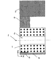
Figure 12 is the resin film at 2 layers of structure, the structure when the median plane of thickness direction partly is provided with the insulating barrier that does not include particle.
Figure 13 is the resin film at 3-tier architecture, the structure when the median plane of thickness direction partly is provided with the insulating barrier that does not include particle.
Figure 14 is the resin film at 4 layers of structure, the structure when the median plane of thickness direction partly is provided with the insulating barrier that does not include particle.
The electrode shape of Figure 15 for being used for resolving.
Figure 16 is the result of calculation about the time variation of the viscosity of resin (1) (2) (3).
Figure 17 is the result of calculation of the particle catch rate of the situation of conductive layer use resin (1) and insulating barrier use resin (1) (2) (3).
Figure 18 is the situation of conductive layer use resin (1) and insulating barrier use resin (1) (2) (3), about the result of calculation of substrate interlude variation.
Figure 19 is the result of calculation about the time variation of the viscosity of resin (1) (4) (6) (7) (8).
Figure 20 is the result of calculation of the particle catch rate of the situation of conductive layer use resin (1), insulating barrier use resin (1) (4) (6) (7) (8).
Figure 21 is the result of calculation about the relation of the exothermic reaction speed of resin (1) (14) and resin temperature.
Figure 22 is the result of calculation of the particle catch rate of the situation of conductive layer use resin (1), insulating barrier use resin (9) (10) (11) (12) (13).
Figure 23 is the resin film at 3-tier architecture, between the insulating barrier that is sandwiched in topmost and undermost conductive layer and the intermediate layer that arranges arrange conductive coefficient low do not include the insulating barrier of particle the time structure.
Figure 24 for expression with (electrode spacing)/(electrode height) of each electrode shape as the figure of transverse axis, (the 1st layer of setting catch sufficient rate)/(the 2nd layer of setting catch sufficient rate) as the result of longitudinal axis arrangement.
Symbol description
1 electroconductive particle
2 resin materials
3 semiconductor integrated circuit (IC)
4 upper electrodes
5 substrates
6 lower electrodes
7 faces that constituted by the central point of the thickness direction of resin film
8 are sandwiched between the insulating barrier of topmost and undermost conductive layer and the insulating barrier that arranges
Embodiment
The execution mode that the present invention relates to is described with reference to the accompanying drawings.At first using Fig. 1 to illustrate becomes the connection of analysis object moulding process.
The positive minus side that Fig. 1 (a) is illustrated in the directions X in XZ cross section arranges the pair of electrodes that should be electrically connected in the structure of electrode with symmetric shape.In addition, Fig. 1 (b) is illustrated in the pair of electrodes that should be electrically connected of extending perpendicular to the Y-direction in the YZ cross section of Fig. 1 (a).
Connecting the A-stage of moulding, the resin material 2 that includes the particle 1 with conductivity is arranged between the lower electrode 6 of the upper electrode 4 of semiconductor integrated circuit (IC) 3 and substrate 5.At this, the height of supposing upper electrode 4 is H
U, lower electrode 6 electrode height be H
S, by H1 (=H
U+ H
S) expression 1 pair of electrode height sum that should be electrically connected, represent electrode 4,6 width by W1, be illustrated in the interval (spacing) of the electrode 4 that the positive minus side of directions X arranges by W2, represented the electrode length of Y-direction by L1.
Move to the direction of substrate 5 about connecting moulding process, make semiconductor integrated circuit (IC) 3 that heat, compression comprises the resin material 2 of particle 1, thereby resin material 2 generations that include particle 1 are mobile.At this moment, by the electrode 4 of semiconductor integrated circuit (IC) 3 and contacting of resin material 2, the temperature of resin material 2 changes, produce viscosity and change on one side be accompanied by variations in temperature, and meanwhile resin material 2 with particle 1 compressed flowing.
Can use the material that in the adhesive composite of the potentiality curing agent that contains epoxy resin, epoxy resin and phenoxy resin, has disperseed electroconductive particle as required as resin material 2.
In addition, the interval of the electrode 4 of semiconductor integrated circuit (IC) 3 and the electrode 6 of substrate 5 deforms compressed than the diameter of particle 1 hour while be clipped in the particle 1 of 4 at electrode.During the mobile end of semiconductor integrated circuit (IC) 3, by being clipped in electrode 4,6 the conductivity of particle 1, just can be at semiconductor integrated circuit (IC) 3 and 5 transmission of electric signals of substrate.
At this, the conductivity of semiconductor integrated circuit (IC) 3 and 5 of substrates is to be decided by the quantity that is connected the particle 1 that is clipped in 6 of upper electrode 4 and lower electrodes after the moulding and particle 1 and electrode 4,6 contact area.Here, conductivity is by estimating at electrode 4,6 electric currents that circulate when applying certain voltage.Thereby, in order to improve electric conductivity, need to improve the population of 6 of the upper electrode 4 that is clipped in after the moulding and lower electrodes.
Describe at the structure that can improve by connecting the resin molding material that is clipped in the particle catch rate that electrode 4,6 the ratio of quantity of particle 1 define after the quantity that is present in the particle 1 in electrode 4,6 the resin molding before the moulding and the moulding in the research below.
The resin molding material use that only is provided with particle 1 at the resin molding material that is made of 2 layer laminate at thickness direction, at 2 layers in 1 layer of resin film layer flows to resolve and studies.Electrode 4,6 and the size Expressing of resin molding material in Fig. 2.Adopt 5 kinds of different electrode shapes 4 like this, set analytic modell analytical model in the equal symmetry of the positive and negative direction of directions X.
At this, in 2 layers resin molding, contact the upper electrode 4 and resin film layer of configuration is defined as the 1st layer, contact the lower electrode 6 and resin film layer of configuration is defined as the 2nd layer, the particle that includes particle 1 the 1st layer or the 2nd layer of configuration arranges layer (conductive layer).Here, the layer (insulating barrier) that Fig. 2 only shows particle, and layer (conductive layer) is set is the 2nd layer, will not include particle is arranged on the 1st layer situation, and the height setting of lower electrode 6 is H
S=0.5 μ m.
At this, the diameter of particle 1 is set at 4 μ m, and the thickness setting that particle arranges layer is three ranks of 4,6,8 μ m, and all thickness of resin molding all is set at 16 μ m.Here, in order to compare, the thickness that layer is set for particle is that the situation of 16 μ m (all thickness at resin molding arranges particle) is also studied.And about the population that includes, the situation that particle arranges the thickness 4 μ m of layer is 200, and the situation of 6 μ m is 300, and the situation of 8 μ m is 400, and the situation of 16 μ m is 800.
In addition, the temperature that makes upper electrode 4 rises to 200 ℃ from 25 ℃ in 10 seconds, and upper electrode 4 is moved to the direction of lower electrode 6.The translational speed of the upper electrode 4 at initial stage is 1 * 10
-3M/s.Here, fluid is resolved and is used fluid commonly used to resolve software.
The viscosity of the translational speed of the upper electrode 4 at consideration initial stage and resin 2 changes and the translational speed of calculating upper electrode 4 in the parsing, and particle 1 imagination ground is arranged in the resin 2 as identifying particle.Here, suppose that the physics value of resin 2 of layers 1 and 2 is identical, will be illustrated in (1)~(5) for the exothermic reaction formula of resolving, the viscosity formula is illustrated in (6)~(8).And resin 2 adopts the epoxy resin that belongs to thermosetting resin, and physics value (coefficient of the coefficient of viscosity formula, exothermic reaction formula) is illustrated in the resin (1) of table 1.In addition, conductive coefficient is 0.2W/ (mK), and specific heat is 1700J/ (kgK), and density is 1100kg/m
3
◎ exothermic reaction formula
dα/dt=(K
1+K
2α
M)(1-α)
N ..(1)
K
1=Ka exp(-Ea/T) ..(2)
K
2=Kb exp(-Eb/T) ..(3)
α=Q/Q0 ..(4)
dQ/dt=Q0(K
1+K
2α
M)(1-α)
N..(5)
At this, α: reactivity, t: time, T: temperature, dA/dt: reaction speed, K
1, K
2: become the coefficient of temperature funtion, Q: by the thermal discharge of any time, Q0: the total thermal discharge when reaction finishes, N, M, Ka, Ea, Kb, Eb: the coefficient that material is intrinsic, dQ/dt: heat release speed.
◎ viscosity formula
η=ηo((1+α/αgel)/(1-α/αgel))
H..(6)
ηo=a·exp(b/T) ..(7)
H=f/T-g ..(8)
At this, η: viscosity, α: reactivity, T: resin temperature, α gel: gelation reaction rate, a, b, f, g: the constant that material is intrinsic.
Adopt this analytic method to calculate the catch rate of particle 1.Here, the catch rate ε (%) of particle 1 is clipped in electrode 4 after the population N1 that is present in before the moulding in electrode 4,6 the resin molding material and the shaping to connect, 6 the ratio of population N2 is calculated by formula (9).
ε=N2/N1×100 ..(9)
The analysis result of the catch rate of particle 1 is illustrated among Fig. 3,4,5,6.
Fig. 3 has compared the catch rate of particle 1 that all thickness at resin molding arranges the situation of particle 1 at each electrode shape, Fig. 4 has compared the catch rate of particle 1 that thickness that particle arranges layer is the situation of 4 μ m at each electrode shape, Fig. 5 compared the catch rate of particle 1 that thickness that particle arranges layer is the situation of 6 μ m at each electrode shape, and Fig. 6 has compared the catch rate of particle 1 that thickness that particle arranges layer is the situation of 8 μ m at each electrode shape.Like this, the particle catch rate is according to each electrode shape and difference, and the thickness that particle the arranges layer more catch rate of small-particle 1 is more high.
Resin material as resin film can use the material that has disperseed electroconductive particle as required in the adhesive composite of the potentiality curing agent that contains epoxy resin, epoxy resin and phenoxy resin.
Fig. 7 is the situation of 8 μ m at shape (1), the thickness that layer is set at the particle that is arranged at the 2nd layer, is that the distribution of resin flows speed of the directions X of 14 μ m utilizes curve to represent ratio (XZ plane) about the distance of 6 of upper electrode 4 and lower electrodes.The ratio of this VELOCITY DISTRIBUTION is the ratio curve plotting of 1 situation with the speed maximum of directions X.
Resin material as resin film can use the material that has disperseed electroconductive particle as required in the adhesive composite of the potentiality curing agent that contains epoxy resin, epoxy resin and phenoxy resin.
Like this, the ratio of the VELOCITY DISTRIBUTION of directions X is that peaked situation is near the core of gauge of 6 of upper electrode 4 and lower electrodes.Thereby, by the become cores of the thickness direction that maximum and particle 1 discharges from electrode 4,6 to the X positive direction easily of the resin flows speed that is formed in directions X, the conductive layer that includes particle 1 is not set but the structure of the insulating barrier that does not include particle 1 is set, can improve the catch rate of particle 1.
That is to say, as shown in figure 12, resin film at 2 layers of structure, the layer of the part of the face 7 that constitutes at the central point by the gauge of any many places of resin molding or face 7 adjacency that are made of the central point of gauge, the structure that the insulating barrier that does not include particle 1 is set is effective to the catch rate that improves particle 1.
Resin material as resin film can use the material that has disperseed electroconductive particle as required in the adhesive composite of the potentiality curing agent that contains epoxy resin, epoxy resin and phenoxy resin.
In addition, as shown in figure 13, use the situation of the resin film of 3-tier architecture, the part setting in the cross section 7 that constitutes by the central point that is formed on by the gauge of any many places of resin molding does not include the structure of the insulating barrier of particle 1, can improve the particle catch rate yet.
Resin material as resin film can use the material that has disperseed electroconductive particle as required in the adhesive composite of the potentiality curing agent that contains epoxy resin, epoxy resin and phenoxy resin.
In addition, as shown in figure 14, use the situation of the resin film of 4 layers of structure, the part setting in the cross section 7 that constitutes by the central point that is formed on by the gauge of any many places of resin molding does not include the structure of the insulating barrier of particle 1, can improve the particle catch rate yet.And it also is same using the situation of the resin film of the structure with more multi-layered resin film layer.
Resin material as resin film can use the material that has disperseed electroconductive particle as required in the adhesive composite of the potentiality curing agent that contains epoxy resin, epoxy resin and phenoxy resin.
About at thickness direction by 2 layers of resin film that includes particle that constitutes with superimposed layer, the thickness of interlayer is than producing deviation sometimes during fabrication.Thereby, about at thickness direction by 2 layers of resin film that includes particle that constitutes with superimposed layer, also can be formed on the face 7 that constitutes from the central point by the gauge of any many places of resin film apart from thick resin film ± 5% do not include the structure of the insulating barrier of particle with interior scope setting, can also make the resin film layer of face 7 adjacency that the central point by the gauge of any many places of resin film constitutes for not including the insulating barrier of particle 1 thus.
At this, shown in Fig. 3~6, by making the thickness attenuation of the rete that is provided with particle 1, can particle 1 be set in the position of the middle body of the thickness direction of 6 of the upper electrode 4 that deviates from the speed maximum and lower electrodes, the particle catch rate increases thus.
The thickness setting of having studied the resin film layer that will include particle 1 in this parsing is the situation of 4,6,8 μ m, in order to improve the catch rate of particle 1, shown in Fig. 3~6, need reduce the thickness that particle arranges layer, preferably thickness is decreased to the equal diameters with particle 1.But, manufacturing has the situation with the resin molding of the thickness of the equal diameters of particle 1, because particle 1 exposes from the resin molding material, because the device specification error of manufacturing installation when the thickness of the film that particle 1 is set than the diameter of particle 1 hour, can produce problem that particle 1 deforms etc. and produce problem on making.
Thereby, in 2 layers only 1 layer of resin film layer be provided with 2 layers of resin film of particle 1, the thickness that particle arranges layer is preferably the diameter of particle 1+below 10%.More than at the resin molding material that is constituted by 2 layer laminate result of study has been described, the present invention is not limited to this, also goes for 3 layers, 4 layers or more multi-layered resin film.
Resin material as resin film can use the material that has disperseed electroconductive particle as required in the adhesive composite of the potentiality curing agent that contains epoxy resin, epoxy resin and phenoxy resin.
Carry out analysis research as an example at the situation that is provided with particle 1 at the resin molding of the layer that contacts with lower electrode 6 with upper electrode 4 among the resin molding material that is constituted by 3 layer laminate and 3 layers.The shape of be used for resolving is identical with electrode shape (1) shown in Figure 2, and the thickness that particle arranges layer is 4 μ m up and down and studies.Particle 1 number that arranges is 400.In addition, about the physics value of resin film layer, 3 layers all identical, is the value of table 1.
When representing that by curve upper/ lower electrode 4,6 distance are the ratio of VELOCITY DISTRIBUTION (XZ plane) of the directions X of 14 μ m as analysis result, the result of calculation of particle catch rate is illustrated among Fig. 9.Like this, with regard to regard to the speed of the directions X on XZ plane, it is maximum that the approximate centre of the thickness direction between upper/lower electrode part (part of particle 1 is not set) becomes, in 3 layers of resin molding the resin molding of the layer that joins with upper electrode 4 and lower electrode 6 be provided with particle 1 situation the particle catch rate than shape shown in Figure 3 (1) to be provided with the situation of particle 1 at all thickness of film also high.
In addition, particle arranges the situation of the thin thickness of layer, can particle 1 be set in the position of departing from directions X speed core maximum, interelectrode thickness direction, can obtain high particle catch rate thus.Thereby, use the situation of 3 layers resin molding material, also same with the situation of 2 tunics with regard to the thickness that the particle at the topmost of film thickness direction and foot arranges layer, be preferably particle diameter+below 10%.
More than position description the has been set structure of resin film at the conductive layer that includes particle, can also be applicable to the electronic unit that uses this resin film to be electrically connected.The situation of the laminated structure of 2 layers of thickness direction or 3 layers more than has been described, but the present invention is not limited to this, can be used for the resin film of the multilayer laminated structure of lamination more than 2 layers.
Resin material as resin film can use the material that has disperseed electroconductive particle as required in the adhesive composite of the potentiality curing agent that contains epoxy resin, epoxy resin and phenoxy resin.
Shown in Fig. 4,5,6, about the particle catch rate, the situation that particle 1 is set which side of the 1st layer of Fig. 2 or the 2nd layer just can obtain high particle catch rate according to electrode shape and be different on earth.At this, will be that the result that the longitudinal axis is put in order is illustrated among Fig. 9 with (at the 1st layer of particle catch rate that is provided with the situation of particle 1)/(at the 2nd layer of particle catch rate that is provided with the situation of particle 1) at each electrode shape.
Here, the situation of (at the 1st layer of particle catch rate that is provided with the situation of particle 1)/(at the 2nd layer of particle catch rate that is provided with the situation of particle 1) greater than 1 be, can obtain the shape of high particle catch rate the 1st layer of situation that is provided with particle 1; The situation of (at the 1st layer of particle catch rate that is provided with the situation of particle 1)/(at the 2nd layer of particle catch rate that is provided with the situation of particle 1) less than 1 be, can obtain the shape of high particle catch rate the 2nd layer of situation that is provided with particle 1.
At this, as shown in Figure 1, suppose that 1 pair of electrode height sum that should connect is H1 (=H
U+ H
S), the mean value of electrode 4,6 width is W1, the interval (spacing) of the electrode 4 that arranges at the positive minus side of directions X is the situation of H2 for W2, particle diameter, with ((W2-W1) * (H1+H2)
3)/(W1 * H2
3) as transverse axis, the result of (at the 1st layer of catch rate that is provided with the situation of particle)/(at the 2nd layer of catch rate that is provided with the situation of particle) as longitudinal axis arrangement is illustrated among Figure 10.
Like this, use the situation of 2 layers of resin film, according to for example ((W2-W1) * (H1+H2) that determined by electrode shape
3)/(W1 * H2
3) value, just can obtain high particle catch rate in the time of just can clearly particle being arranged on which side of the 1st layer or the 2nd layer.
That is to say, for example ((W2-W1) * (H1+H2)
3)/(W1 * H2
3) value less than 50 situation, at the rete with electrode 6 sides of high electrode 4 opposition sides of electrode height particle 1 is set; ((W2-W1) * (H1+H2)
3)/(W1 * H2
3) value be situation more than 90, at the rete of high electrode 4 sides of electrode height particle 1 is set, can increase the catch rate of particle 1 thus, so just can adopt the electrode shape that is suitable for electronic unit or the resin film of electrode structure.
Resin material as resin film can use the material that has disperseed electroconductive particle as required in the adhesive composite of the potentiality curing agent that contains epoxy resin, epoxy resin and phenoxy resin.
The shape of electrode is ((W2-W1) * (H1+H2) for example
3)/(W1 * H2
3) value be situation more than 90, in the last stage of the connection moulding of having used 2 layers of resin film the electronic unit that particle 1 connects moulding is set in the rete of high electrode 4 sides of electrode height and can improves the particle catch rate.
Among Figure 24 expression with (electrode spacing)/(electrode height) of each electrode shape as the figure of transverse axis, (the 1st layer of setting catch sufficient rate)/(the 2nd layer of setting catch sufficient rate) as the result of longitudinal axis arrangement.
Like this, (electrode spacing)/(electrode height) is 0.7 when above, in the last stage of the connection moulding of having used 2 layers of resin film, in the rete of high electrode 4 sides of electrode height, particle 1 is set and the electronic unit that connects moulding can improve the particle catch rate.
At this, use the situation of the electrode shape (1) of Fig. 2,2 layers of all thickness of resin molding are changed to 10,12,14,16 μ m study.In addition, the thickness that is provided with the layer of particle 1 changes to 4,6,8 μ m, and about the physics value of the resin material of all layers, exothermic reaction formula and viscosity formula are according to formula (1)~(8), and each parameter is used the value of table 1.
The result of particle catch rate is illustrated among Figure 11.Like this, same with the result of Fig. 3~6 expressions, the little situation of thickness that layer is set of particle 1 can obtain high particle catch rate.And then all thickness of resin molding hour can obtain the catch rate of high particle 1.To reduce be because resin and particle increase to the discharge rate of Y-direction shown in Figure 1 to the particle catch rate when in addition, all thickness of resin molding was big.
Put down in writing thickness that particle arranges layer in the paragraph in front and be preferably the diameter of particle 1+below 10%, but the thickness of particle and film situation about equally need suppress the deviation of thickness and make particle not outstanding from film, so the film manufacturing cost can increase sometimes.
Thereby, for the catch rate of particle as shown in figure 11 can be as high as more than 30%, realize that by improving the population that between electrode, catches cost reduces, the all most preferred thickness of film is the diameter+below 10% of above-mentioned particle 1, secondly preferred film thickness 6/4=1.5 that is particle doubly below, more secondly preferred thickness be 8/4=2 doubly below.
Result of study at the resin molding material that is made of 2 layer laminate more than has been described, but the present invention is not limited to this, also go for 3 layers, 4 layers or more multi-layered resin film.
In addition, the thickness that layer is set as particle and the ratio of the thickness of the layer that particle is not set preferred as shown in figure 11 for the particle catch rate can be increased to 48% or more more than NCF layer thickness/ACF layer thickness=6/4=1.5 times.
In addition, the high situation of height of the electrode that is connected by film needs to increase all thickness of film.At this moment, secondly the ratio of preferred NCF layer thickness/ACF layer thickness for can make the particle catch rate be 45% or more more than NCF layer thickness/ACF layer thickness=10/4=2.5 times.Secondly preferably can make again the particle catch rate be 40% or more more than NCF layer thickness/ACF layer thickness=12/4=3 times.
Result of study at the resin molding material that is made of 2 layer laminate more than has been described, but the present invention is not limited to this, also go for 3 layers, 4 layers or more multi-layered resin film.
Thereby, in order to improve the particle catch rate, need reduce all thickness of resin molding, still consider the adhesive strength of resin molding and electrode 4 etc., the amount that the cross section resin material on XZ plane shown in Figure 1 is filled is minimum also to be needs.
At this, suppose that as shown in Figure 11 pair of electrode height sum that should connect is H1 (=H
U+ H
S), the mean value of electrode 4,6 width is W1, the interval (spacing) of the electrode 4 that arranges at the positive minus side of directions X is the situation of W2, the movement by upper electrode 4 is represented by formula (9) at the minimum thickness Hmin that as shown in Figure 1 XZ plane resin material is filled required resin molding.
[0155] Hmin=((W2-W1)/W2)×H1 ……(9)
[0156]But owing to need to arrange particle in the resin molding, all thickness of resin molding that can improve the particle catch rate is preferably below " Hmin=((W2-W1)/W2) * H1+ particle diameter) ".
Thereby, by the electronic unit that is electrically connected by the resin molding material that includes particle that constitutes more than 1 layer, if being arranged on interelectrode all thickness by the resin molding material that includes particle 1 that constitutes more than 1 layer in the last stage that connects moulding for example is that then the electronic unit that is electrically connected by the resin molding that includes particle just can obtain high particle catch rate below " ((W2-W1)/W2) * H1+ particle diameter) ".
The layer that the particle that resin molding material more than 2 layers more than has been described arranges layer and particle is not set is not divided into the example of multilayer, but the present invention is not limited to this, and the layer that particle arranges layer and particle is not set can be divided into more than 2 layers.
In addition, more than the particle of resin molding material more than 2 layers layer is set and the physics value of layer of particle is not set all identical and adopted the value of table 1, still the present invention is not limited to this, can adopt the resin molding of the different physics value of each layer.And, the analysis result that uses epoxy resin more than has been described, but the present invention is not limited to this, can use resin material arbitrarily.
Physics value at the resin molding material that can improve the particle catch rate in the following research describes, here, the particle catch rate be by be clipped in electrode 4 after connecting the quantity that is present in the particle 1 in electrode 4,6 the resin molding before the moulding and being connected moulding, 6 the ratio of quantity of particle 1 defines.
Resin material as resin film can use the material that has disperseed electroconductive particle as required in the adhesive composite of the potentiality curing agent that contains epoxy resin, epoxy resin and phenoxy resin.
In at the resin molding material that is constituted by 2 layer laminate at thickness direction, to 2 layers only resin molding material with the conductive layer that is provided with particle 1 of 1 layer of resin film layer use to flow to resolve and study.Electrode 4,6 and the size Expressing of resin molding material in Figure 15.Here, the equal symmetry and set analytic modell analytical model of the positive negative sense of directions X.
At this, in 2 layers the resin molding, the resin film layer that contacts with upper electrode 4 and dispose is defined as the 1st layer, the resin film layer that contacts with lower electrode 6 and dispose is defined as the 2nd layer, particle is arranged layer (conductive layer) be arranged to the 2nd layer, the layer (insulating barrier) that will not include particle 1 is arranged to the 1st layer, the height H s=0.5 μ m of lower electrode 6.
At this, particle diameter is set at 4 μ m, the thickness setting that particle arranges layer is 8 μ m, all thickness settings of resin molding are 16 μ m.And the population that includes is 400.
In addition, the temperature that makes upper electrode 4 rises to 200 ℃ from 25 ℃ in 10 seconds, because the temperature rising resin molding of this upper electrode 4 is heated.And upper electrode 4 moves to the direction of lower electrode 6, and the translational speed of the upper electrode 4 at initial stage is 1 * 10
-3M/s.Here, will use fluid always and resolve software for the fluid parsing.
The viscosity of the translational speed of the upper electrode 4 at consideration initial stage and resin 2 changes and the translational speed of calculating upper electrode 4 in the parsing, and particle 1 imagination ground is arranged in the resin 2 as identifying particle.Here, the exothermic reaction formula that is used for resolving adopts formula (1)~(5), and the viscosity formula adopts formula (6)~(8).At this, about the coefficient of the viscosity formula shown in formula (6)~(8), the 2nd layer conductive layer adopts the value of resin material (1), and the 1st layer insulating barrier adopts the value of these three kinds of resin materials of resin material (1) (2) (3).On the other hand, about the coefficient of the exothermic reaction formula shown in formula (1)~(5), the value of layers 1 and 2 is identical and adopt the value of resin material (1).In addition, resin 2 adopts the epoxy resin as thermosetting resin, is illustrated in the table 1 about the physics value (coefficient of the coefficient of viscosity formula, exothermic reaction speed mode, density, conductive coefficient, specific heat) of resin (1)~(3).

Use this analytic method to calculate the catch rate of particle 1.At this, utilize the result of the time variation of resolving the viscosity of obtaining setting to be illustrated among Figure 16.Like this, the MV minium viscosity of material (1) is set for higher 1.3 times than material (2), than low 1.3 times of material (3).In addition, reduce in order to make material (3) compare MV minium viscosity with material (1), for example make weight average molecular weight littler than material (1).
The analysis result of the catch rate of particle 1 is illustrated among Figure 17, and substrate 4,6 interlude change list are shown among Figure 18.
As shown in figure 17, even the viscosity of the conductive layer of the 1st layer insulating barrier and the 2nd layer there are differences, the particle catch rate can not create a difference yet.Use the result of Figure 18 to investigate the reason that this particle catch rate does not create a difference.Figure 18 represents that the substrate interlude changes, and is clipped in population between substrate and the catch rate of particle just is determined in the moment that substrate is spaced apart the 4 μ m that equate with particle diameter.
As shown in figure 18, time of equating with particle diameter at interval of substrate is about 1.5s.But as shown in figure 16, the following setting of viscosity of current resin material (1)~(3 of setting): the time variation that ends the viscosity of 1.5s equates that only MV minium viscosity there are differences.Thereby changing by the viscosity of 1.5s that the particle catch rate is determined can not produce difference, even think that thus the result is that the viscosity of the conductive layer of the 1st layer insulating barrier and the 2nd layer as shown in figure 16 there are differences, the particle catch rate can not create a difference yet.
Like this, even there are differences, the MV minium viscosity of the conductive layer of the 1st layer insulating barrier and the 2nd layer can not improve the particle catch rate.Thereby, below study for the material that there are differences in the conductive layer viscosity of using the 1st layer insulating barrier and the 2nd layer by the initial stage of the connection moulding of 1.5s.
Adopt the shape of Figure 15 in the parsing, particle diameter is set at 4 μ m, the thickness setting that the 2nd layer particle arranges layer (conductive layer) is three ranks of 4,6,8 μ m, and all thickness settings of resin film are 16 μ m.At this, about the viscosity formula shown in formula (6)~(8), the 2nd layer conductive layer uses resin material (1), and the 1st layer insulating barrier uses resin material (1), (4)~(8).On the other hand, about the exothermic reaction formula shown in formula (1)~(5), the identical and employing resin material (1) of the physics value of layers 1 and 2.In addition, resin 2 adopts the epoxy resin as thermosetting resin, is illustrated in the table 1 about the physics value (viscosity, density, conductive coefficient, specific heat, exothermic reaction) of resin (1), (4)~(8).
At this, set for: the viscosity that resin (4) was compared with resin (1) before 25 ℃ be connected is 2 times, the viscosity that resin (5) was compared with resin (1) before 25 ℃ be connected is 1/1.2 times, the viscosity that resin (6) was compared with resin (1) before 25 ℃ be connected is 1/2 times, the viscosity that resin (7) was compared with resin (1) before 25 ℃ be connected is 1/5 times, and the viscosity that resin (8) was compared with resin (1) before 25 ℃ be connected is 1/10 times.
Resin material as resin film can use the material that has disperseed electroconductive particle as required in the adhesive composite of the potentiality curing agent that contains epoxy resin, epoxy resin and phenoxy resin.
In addition, the temperature of upper electrode 4 rises to 200 ℃ from 25 ℃ in 10 seconds, and upper electrode 4 moves to the direction of lower electrode 6.The translational speed of the upper electrode 4 at initial stage is 1 * 10
-3M/s.And, for material (4) and material (1) phase specific viscosity height, for example make weight average molecular weight bigger than material (1).
The result of calculation that the time of the resin viscosity of be used for resolving changes is illustrated in Figure 19.At this, change to be illustrated at the viscosity of resin (1), (4), (6), (8), the viscosity gauge of time 0s is shown in the viscosity before 25 ℃ the connection moulding.Like this, by resin (5)~(8) being used for the 1st layer insulating barrier, can give and resin (1) differences in viscosity of state in the early stage that is used for the 2nd layer conductive layer.
The analysis result of particle catch rate is illustrated among Figure 20.When such the 1st layer insulating barrier adopted resin (4), because the ratio of viscosities of insulating barrier conduction floor height, by the compression between substrate, the resin material of the conductive layer that viscosity is low took place to flow, and the resin material of conductive layer is difficult to remain between substrate, and the particle catch rate reduces.
On the other hand, when the 1st layer insulating barrier adopts resin (5)~(8), because the ratio of viscosities conductive layer of insulating barrier is low, by the compression between substrate, the resin material of the insulating barrier that viscosity is low takes place to flow, the resin material of conductive layer remains between substrate easily, and the more big then particle of the differences in viscosity of insulating barrier and conductive layer catch rate is more high.In addition, it is more high to be provided with the more little then particle of the thickness catch rate of conductive layer of particle.
Like this, about the resin of the conductive layer that is used for the 1st layer insulating barrier and the 2nd layer, make the 1st layer insulating barrier when 25 ℃ viscosity is lower than the 2nd layer conductive layer, can improve the particle catch rate.Particularly, the 1st layer insulating barrier is compared with the 2nd layer conductive layer when being low to moderate below 0.5 times 25 ℃ viscosity, can improve the particle catch rate.In addition, about the mensuration of viscosity, adopt the rotary-type viscosimeter that has utilized parallel-plate or cone-plate, the state that comprises particle at the rete that includes particle carries out the mensuration of the film before 25 ℃ connection moulding with shear rate 0.1 (1/s).
In the above result who has illustrated about 2 layers resin molding, but the present invention is not limited to this, goes for the resin sheet with the random layer lamination more than 2 layers.And, give differences in viscosity to 2 layers and study above, but the present invention is not limited to this, by forming the structure that the maximum of comparing the exothermic reaction speed that the insulative resin rete measured by differential scanning calorimetry (DSC) with the resin film layer that includes electroconductive particle is in low temperature side, can improve the particle catch rate.
For example at the resin shown in the table 1 (14) and resin (1), be that the measurement result of differential scanning calorimetry (DSC) of the relation of the relevant exothermic reaction speed of situation of 5 ℃/min and resin temperature is illustrated in Figure 21 to the resin (14) that is used for the 2nd layer (conductive layer) and the exothermic reaction speed (dQ/dt) that is used for the resin (1) of the 1st layer (insulating barrier), to programming rate.Like this, resin (14) reaction speed under low resin temperature is maximum.
In addition, the 1st layer, the 2nd layer viscosity all adopts equal value as shown in table 1.Thus, exothermic reaction speed is maximum under low resin temperature, and the viscosity as the function of α (reactivity) of formula (6)~(8) expression increases at low temperatures.Thereby, when the maximum of exothermic reaction speed of comparing the 2nd layer conductive layer with the 1st layer insulating barrier is in low temperature side, the insulation floor height that the ratio of viscosities of the 2nd layer conductive layer is the 1st layer even also be difficult to take place to flow by the compression of substrate, therefore can obtain high particle catch rate.Here, the mensuration of exothermic reaction speed adopts the differential calorimeter, and in the relation of exothermic reaction speed shown in Figure 8 and resin temperature, the resin that the maximum of exothermic reaction speed is in low temperature side is used for conductive layer.
Then, situation about there are differences for the conductive coefficient of the conductive layer of the 1st layer insulating barrier and the 2nd layer particle catch rate that utilized analysis research.Adopt the shape of Figure 12 in the parsing, particle diameter is set at 4 μ m, the thickness setting that the 2nd layer particle arranges layer (conductive layer) is two ranks of 4,8 μ m, and all thickness of resin film all is set at 16 μ m.
About by the exothermic reaction formula shown in formula (1)~(5), by the viscosity formula shown in formula (6)~(8), the 2nd layer conductive layer adopts the resin (1) shown in the table 1.Adopt by the exothermic reaction formula shown in formula (1)~(5), identical with resin (1) by the viscosity formula shown in formula (6)~(8) for the 1st layer insulating barrier, just low resin (9)~(13) of thermal conductivity ratio resin (1).The physics value of resin (9)~(13) is illustrated in the table 1.In addition, for the conductive coefficient of material (9)~(13) is lower than resin (1), for example cooperate low heat fillings such as mica.
In addition, the temperature of upper electrode 4 rises to 200 ℃ from 25 ℃ in 10 seconds, and upper electrode 4 moves to the direction of lower electrode 6.The translational speed of the upper electrode 4 at initial stage is 1 * 10
-3M/s.Here, the mobile parsing adopts fluid commonly used to resolve software.
The analysis result of particle catch rate is illustrated among Figure 22.The thickness that Figure 22 (a) expression is provided with the conductive layer of particle is the result of 8 μ m situations, and the thickness that Figure 22 (b) expression is provided with the conductive layer of particle 1 is the result of 4 μ m situations.Like this, the conductive coefficient of the 1st layer insulating barrier is lower than the situation of conductive coefficient of the 2nd layer conductive layer, can obtain high particle catch rate.At this moment,,, when hanging down, the conductive coefficient of the 1st layer insulating barrier is difficult to the 2nd layer conductive layer heat conduction to resin film heat conduction from upper electrode 4, so the ratio of viscosities of conductive layer insulation floor height.Thereby by interelectrode compression, the resin of conductive layer is difficult to flow, and can obtain high particle catch rate thus.Particularly, as shown in figure 22, compare with the 2nd layer the conductive layer that includes conducting particles, make the 1st layer the conductive coefficient of the insulating barrier that does not include conducting particles little to below 0.7 times the time, can improve the particle catch rate.
In addition, the thickness that is provided with the conductive layer of particle is the situation of 4 μ m, because it is big that the thickness of the insulating barrier that the 1st layer conductive coefficient is low becomes, be that the situation of 8 μ m is compared the conductive layer heat conduction that more is difficult to the 2nd layer with the thickness of conductive layer, therefore can obtain high particle catch rate.
In addition, more than be illustrated at the resin film of 2 layer laminate, but the present invention is not limited to this, can be used for 2 layers of resin film with superimposed layer.Figure 23 illustrates the resin film of 3 layer laminate as an example.At this, it is characterized in that, topmost at the thickness direction of the formation outermost surface of resin film arranges insulating barrier, at foot conductive layer is set, is sandwiched between the conductive layer of the insulating barrier of topmost and foot and insulating barrier and the undermost conductive layer of the above-mentioned topmost of the thermal conductivity ratio of the insulating barrier 8 that arranges are low.
Because this conductive coefficient that is clipped in the insulating barrier 8 that arranges between the conductive layer of the insulating barrier of topmost and foot is little, be difficult to undermost conductive layer heat conduction, the viscosity of conductive layer can not reduce, and the resin by interelectrode compression conductive layer is difficult to flow, and can obtain high particle catch rate thus.Here, thermal Conductivity Determination be comprise the state of particle at the rete that includes particle, resin molding before use connecting moulding carries out in the mensuration temperature below 25 ℃.
The layer that the particle that resin molding material more than 2 layers more than has been described arranges layer and particle is not set is not divided into the example of multilayer, but the present invention is not limited to this, and the layer that particle arranges layer and particle is not set can be divided into more than 2 layers.
In addition, the analysis result that uses epoxy resin more than has been described, but the present invention is not limited to this, can use resin material arbitrarily.
In addition, more than individually be described at the difference of the physics value that position and conductive layer and insulating barrier are set of particle, but the present invention is not limited to this, with regard to regard to the resin film that includes electroconductive particle of thickness direction lamination resin film layer more than 2 layers, comprise in inside the thickness direction that is in equidistance from two surfaces of resin film median plane resin film layer or with at least one resin film layer of the median plane adjacency of above-mentioned thickness direction by the resin film that the resin film layer of the insulating properties that does not include above-mentioned electroconductive particle forms, can also use with following resin film as feature: the low resin film of ratio of viscosities conductive layer of the insulating barrier before 25 ℃ connection moulding; Perhaps insulating barrier is compared the resin film that is in low temperature side by the maximum of the exothermic reaction speed of differential scanning calorimetry (DSC) mensuration with conductive layer; The perhaps low resin film of thermal conductivity ratio conductive layer of insulating barrier.
Claims (6)
1. a resin film is characterized in that, will include each layer of the resin film layer of the resin film layer of electroconductive particle and insulating properties, possessing 1 layer mode at least in the thickness direction lamination more than 3 layers,
Inside comprise the thickness direction that is in equidistance from two surfaces of this resin film median plane resin film layer or with at least one resin film layer of described median plane adjacency, formed by the resin film layer of described insulating properties,
Formed by the resin film layer that includes electroconductive particle with the resin film layer both sides at the two ends of the topmost that is in thickness direction of two surperficial adjacency of this resin film and foot,
The thickness of the thickness direction of the described resin film layer that includes electroconductive particle is configured to be in the resin film layer both sides at two ends of described topmost and foot all greater than the particle diameter of described electroconductive particle and less than 2 times of the particle diameter of described electroconductive particle.
2. resin film according to claim 1, it is characterized in that the thickness of the thickness direction of the described resin film layer that includes electroconductive particle is configured to be in the resin film layer both sides at two ends of described topmost and foot all greater than the particle diameter of described electroconductive particle and less than 1.5 times of the particle diameter of described electroconductive particle.
3. resin film according to claim 1, it is characterized in that the described resin film layer that includes electroconductive particle is configured to be in the resin film layer both sides at two ends of described topmost and foot all greater than the particle diameter of described electroconductive particle and less than 1.1 times of the particle diameter of described electroconductive particle at the thickness of thickness direction.
4. resin film according to claim 1 is characterized in that, the resin film layer of described insulating properties the thickness of thickness direction be configured to for the described resin film layer of electroconductive particle that includes at more than 1.5 times of thickness of thickness direction.
5. resin film according to claim 1 is characterized in that, the resin film layer of described insulating properties the thickness of thickness direction be configured to for the described resin film layer of electroconductive particle that includes at more than 2.5 times of thickness of thickness direction.
6. resin film according to claim 1 is characterized in that, the resin film layer of described insulating properties the thickness of thickness direction be configured to for the described resin film layer of electroconductive particle that includes at more than 3 times of thickness of thickness direction.
Priority Applications (1)
| Application Number | Priority Date | Filing Date | Title |
|---|---|---|---|
| CN201110251065.XA CN102298988B (en) | 2008-06-26 | 2009-06-25 | The resin film including electroconductive particle and the electronic unit electrically connected by it |
Applications Claiming Priority (6)
| Application Number | Priority Date | Filing Date | Title |
|---|---|---|---|
| JP2008167454 | 2008-06-26 | ||
| JP2008-167454 | 2008-06-26 | ||
| JP2008167454 | 2008-06-26 | ||
| JP2009148551A JP4623224B2 (en) | 2008-06-26 | 2009-06-23 | Resin film sheet and electronic parts |
| JP2009148551 | 2009-06-23 | ||
| JP2009-148551 | 2009-06-23 |
Related Child Applications (3)
| Application Number | Title | Priority Date | Filing Date |
|---|---|---|---|
| CN2011102511046A Division CN102298989A (en) | 2008-06-26 | 2009-06-25 | Resin diaphragm having conductive particles inside and electronic components electrically connected by the same |
| CN2011102510630A Division CN102298987A (en) | 2008-06-26 | 2009-06-25 | Use of resin diaphragm |
| CN201110251065.XA Division CN102298988B (en) | 2008-06-26 | 2009-06-25 | The resin film including electroconductive particle and the electronic unit electrically connected by it |
Publications (2)
| Publication Number | Publication Date |
|---|---|
| CN101615446A CN101615446A (en) | 2009-12-30 |
| CN101615446B true CN101615446B (en) | 2013-07-17 |
Family
ID=41495036
Family Applications (4)
| Application Number | Title | Priority Date | Filing Date |
|---|---|---|---|
| CN201110251065.XA Expired - Fee Related CN102298988B (en) | 2008-06-26 | 2009-06-25 | The resin film including electroconductive particle and the electronic unit electrically connected by it |
| CN2011102511046A Pending CN102298989A (en) | 2008-06-26 | 2009-06-25 | Resin diaphragm having conductive particles inside and electronic components electrically connected by the same |
| CN2009101503914A Expired - Fee Related CN101615446B (en) | 2008-06-26 | 2009-06-25 | Rein membrane containing conductive particles and electronic component electrically connected with the same |
| CN2011102510630A Pending CN102298987A (en) | 2008-06-26 | 2009-06-25 | Use of resin diaphragm |
Family Applications Before (2)
| Application Number | Title | Priority Date | Filing Date |
|---|---|---|---|
| CN201110251065.XA Expired - Fee Related CN102298988B (en) | 2008-06-26 | 2009-06-25 | The resin film including electroconductive particle and the electronic unit electrically connected by it |
| CN2011102511046A Pending CN102298989A (en) | 2008-06-26 | 2009-06-25 | Resin diaphragm having conductive particles inside and electronic components electrically connected by the same |
Family Applications After (1)
| Application Number | Title | Priority Date | Filing Date |
|---|---|---|---|
| CN2011102510630A Pending CN102298987A (en) | 2008-06-26 | 2009-06-25 | Use of resin diaphragm |
Country Status (4)
| Country | Link |
|---|---|
| JP (9) | JP4623224B2 (en) |
| KR (8) | KR101038614B1 (en) |
| CN (4) | CN102298988B (en) |
| TW (3) | TWI396626B (en) |
Families Citing this family (17)
| Publication number | Priority date | Publication date | Assignee | Title |
|---|---|---|---|---|
| JP4623224B2 (en) * | 2008-06-26 | 2011-02-02 | 日立化成工業株式会社 | Resin film sheet and electronic parts |
| WO2013132831A1 (en) * | 2012-03-06 | 2013-09-12 | 東洋インキScホールディングス株式会社 | Conductive fine particles, method for manufacturing same, conductive resin composition, conductive sheet, and electromagnetic shielding sheet |
| JP6221285B2 (en) * | 2013-03-21 | 2017-11-01 | 日立化成株式会社 | Circuit member connection method |
| JP6069153B2 (en) * | 2013-09-27 | 2017-02-01 | デクセリアルズ株式会社 | Underfill material and method for manufacturing semiconductor device using the same |
| JP6645730B2 (en) * | 2014-01-28 | 2020-02-14 | デクセリアルズ株式会社 | Connection body and method for manufacturing connection body |
| JP6307308B2 (en) * | 2014-03-06 | 2018-04-04 | デクセリアルズ株式会社 | Manufacturing method of connection structure and circuit connection material |
| KR102430609B1 (en) * | 2014-03-31 | 2022-08-08 | 데쿠세리아루즈 가부시키가이샤 | Anisotropic conductive film and production method therefor |
| KR101737173B1 (en) | 2014-07-24 | 2017-05-17 | 삼성에스디아이 주식회사 | Anisotropic conductive films, a method for preparing the same, and semiconductive devices comprising the same |
| TWI715542B (en) * | 2014-11-12 | 2021-01-11 | 日商迪睿合股份有限公司 | Light curing anisotropic conductive adhesive, method for producing connector and method for connecting electronic components |
| JP6661886B2 (en) * | 2015-03-11 | 2020-03-11 | 日立化成株式会社 | Method for producing film-like circuit connection material and circuit member connection structure |
| KR101684144B1 (en) | 2015-07-08 | 2016-12-07 | 울산대학교 산학협력단 | High efficiency wave energy converter using continuously variable transmission and control method thereof |
| JP6327630B1 (en) * | 2017-04-28 | 2018-05-23 | リンテック株式会社 | Film-like fired material, film-like fired material with support sheet, method for producing film-like fired material, and method for producing film-like fired material with support sheet |
| WO2019050006A1 (en) * | 2017-09-11 | 2019-03-14 | 日立化成株式会社 | Adhesive film for circuit connection and method for manufacturing same, method for manufacturing circuit connection structure, and adhesive tape-containing set |
| JP7210846B2 (en) * | 2017-09-11 | 2023-01-24 | 株式会社レゾナック | Adhesive film for circuit connection, manufacturing method thereof, manufacturing method of circuit connection structure, and adhesive film housing set |
| JP2020024937A (en) * | 2019-10-28 | 2020-02-13 | 日立化成株式会社 | Film-like circuit connection material and method for manufacturing connection structural body of circuit member |
| KR20210154293A (en) | 2020-06-11 | 2021-12-21 | 현대자동차주식회사 | Lithium ion secondary battery and manufacturing method of the same |
| KR20220019470A (en) | 2020-08-10 | 2022-02-17 | 현대자동차주식회사 | System and method for manufacturing lithium ion secondary battery |
Citations (1)
| Publication number | Priority date | Publication date | Assignee | Title |
|---|---|---|---|---|
| CN1210614A (en) * | 1996-02-08 | 1999-03-10 | 旭化成工业株式会社 | Anisotropic conductive composition |
Family Cites Families (21)
| Publication number | Priority date | Publication date | Assignee | Title |
|---|---|---|---|---|
| JPS63102110A (en) * | 1986-10-17 | 1988-05-07 | 富士ゼロックス株式会社 | Anisotropic conductor and making thereof |
| JPH03107888A (en) * | 1989-09-21 | 1991-05-08 | Sharp Corp | Connecting structure for circuit board |
| JPH0645204A (en) * | 1992-07-21 | 1994-02-18 | Nippon Chemicon Corp | Solid electrolytic capacitor |
| JPH0645024A (en) * | 1992-07-22 | 1994-02-18 | Hitachi Chem Co Ltd | Anisotropic conductive adhesive film |
| JPH08148213A (en) * | 1994-11-25 | 1996-06-07 | Hitachi Chem Co Ltd | Connection member and structure and method for connecting electrode using the same |
| GB2296845A (en) * | 1995-01-04 | 1996-07-10 | Plessey Semiconductors Ltd | Frequency shift keyed radio receivers |
| JP3656768B2 (en) * | 1995-02-07 | 2005-06-08 | 日立化成工業株式会社 | Connection member, electrode connection structure using the connection member, and connection method |
| JP4032439B2 (en) * | 1996-05-23 | 2008-01-16 | 日立化成工業株式会社 | Connection member, electrode connection structure and connection method using the connection member |
| JPH10200243A (en) * | 1997-01-13 | 1998-07-31 | Toshiba Chem Corp | Electrical connecting method using anisotropic conductive paste |
| JP2000182691A (en) * | 1998-12-17 | 2000-06-30 | Hitachi Chem Co Ltd | Circuit connecting member and connection method using therewith |
| WO2001071854A1 (en) * | 2000-03-23 | 2001-09-27 | Sony Corporation | Electrical connection material and electrical connection method |
| JP2004006417A (en) | 2003-08-22 | 2004-01-08 | Hitachi Chem Co Ltd | Connecting element and connection structure of electrode using this |
| JP2005146044A (en) * | 2003-11-12 | 2005-06-09 | Sumitomo Electric Ind Ltd | Anisotropic conductive adhesive |
| JP4728665B2 (en) * | 2004-07-15 | 2011-07-20 | 積水化学工業株式会社 | Conductive fine particles, method for producing conductive fine particles, and anisotropic conductive material |
| JP2006233202A (en) * | 2005-01-31 | 2006-09-07 | Asahi Kasei Electronics Co Ltd | Anisotropically electroconductive adhesive film for circuit connection |
| JP4877230B2 (en) * | 2005-11-18 | 2012-02-15 | 日立化成工業株式会社 | Adhesive composition, circuit connection material, connection structure, and circuit member connection method |
| JP4967482B2 (en) * | 2006-02-27 | 2012-07-04 | 日立化成工業株式会社 | Conductive particles, adhesive composition and circuit connecting material |
| EP2015399A4 (en) * | 2006-04-11 | 2013-01-30 | Jsr Corp | Anisotropic conductive connector and anisotropic conductive connector device |
| JP5388572B2 (en) * | 2006-04-27 | 2014-01-15 | デクセリアルズ株式会社 | Conductive particle arrangement sheet and anisotropic conductive film |
| JP2008112732A (en) * | 2007-11-19 | 2008-05-15 | Hitachi Chem Co Ltd | Connecting method of electrode |
| JP4623224B2 (en) * | 2008-06-26 | 2011-02-02 | 日立化成工業株式会社 | Resin film sheet and electronic parts |
-
2009
- 2009-06-23 JP JP2009148551A patent/JP4623224B2/en not_active Expired - Fee Related
- 2009-06-25 TW TW100142306A patent/TWI396626B/en not_active IP Right Cessation
- 2009-06-25 TW TW099127941A patent/TWI415144B/en not_active IP Right Cessation
- 2009-06-25 CN CN201110251065.XA patent/CN102298988B/en not_active Expired - Fee Related
- 2009-06-25 TW TW098121389A patent/TW201013710A/en unknown
- 2009-06-25 KR KR1020090057037A patent/KR101038614B1/en not_active IP Right Cessation
- 2009-06-25 CN CN2011102511046A patent/CN102298989A/en active Pending
- 2009-06-25 CN CN2009101503914A patent/CN101615446B/en not_active Expired - Fee Related
- 2009-06-25 CN CN2011102510630A patent/CN102298987A/en active Pending
-
2010
- 2010-07-12 JP JP2010157800A patent/JP4970574B2/en not_active Expired - Fee Related
- 2010-07-12 JP JP2010157782A patent/JP4661985B2/en not_active Expired - Fee Related
- 2010-07-12 JP JP2010158078A patent/JP4766185B2/en not_active Expired - Fee Related
- 2010-07-12 JP JP2010158022A patent/JP4661986B2/en not_active Expired - Fee Related
- 2010-09-01 KR KR1020100085249A patent/KR101120277B1/en active IP Right Grant
-
2011
- 2011-06-07 JP JP2011127061A patent/JP2011233529A/en not_active Withdrawn
- 2011-06-07 JP JP2011127070A patent/JP2011233530A/en active Pending
- 2011-06-07 JP JP2011127055A patent/JP2011233528A/en not_active Withdrawn
- 2011-06-07 JP JP2011127062A patent/JP2011198767A/en not_active Withdrawn
- 2011-07-08 KR KR1020110067984A patent/KR101120253B1/en not_active IP Right Cessation
- 2011-07-08 KR KR1020110067975A patent/KR20110084489A/en not_active Application Discontinuation
- 2011-07-08 KR KR1020110067977A patent/KR20110084490A/en not_active Application Discontinuation
- 2011-07-08 KR KR1020110067981A patent/KR20110084491A/en not_active Application Discontinuation
- 2011-07-08 KR KR1020110067974A patent/KR20110084488A/en not_active Application Discontinuation
- 2011-11-16 KR KR1020110119297A patent/KR101200148B1/en active IP Right Grant
Patent Citations (1)
| Publication number | Priority date | Publication date | Assignee | Title |
|---|---|---|---|---|
| CN1210614A (en) * | 1996-02-08 | 1999-03-10 | 旭化成工业株式会社 | Anisotropic conductive composition |
Non-Patent Citations (3)
| Title |
|---|
| JP昭63-102110A 1988.05.07 |
| JP特开平10-200243A 1998.07.31 |
| JP特开平9-312176A 1997.12.02 |
Also Published As
Similar Documents
| Publication | Publication Date | Title |
|---|---|---|
| CN101615446B (en) | Rein membrane containing conductive particles and electronic component electrically connected with the same | |
| TWI455151B (en) | Circuit connecting material, film-form circuit connecting material using the same, circuit member connecting structure and method of manufacturing the same | |
| KR101376002B1 (en) | Adhesive composition, circuit connecting material using the same, method for connecting circuit members, and circuit connection structure | |
| KR101659128B1 (en) | Anisotropic conductive film and the semiconductor device using thereof | |
| CN104718234B (en) | Electronic component-use solidification compound and connection structural bodies | |
| TW201218883A (en) | Circuit connection structure | |
| CN110312772A (en) | Adhesive film | |
| JP2012041540A (en) | Circuit connecting material, connecting method using the same, and connection structure | |
| JP2013149467A (en) | Anisotropic conductive film, connection structure and method for producing connection structure | |
| KR20190081985A (en) | Anisotropic conductive film, display device comprising the same and/or semiconductor device comprising the same | |
| JP2015167186A (en) | Method of manufacturing connection structure, and connection structure | |
| US20230002644A1 (en) | Connector production method and adhesive film | |
| JP6398416B2 (en) | Connection structure manufacturing method and connection structure | |
| KR101447125B1 (en) | Anisotropic conductive film |
Legal Events
| Date | Code | Title | Description |
|---|---|---|---|
| C06 | Publication | ||
| PB01 | Publication | ||
| C10 | Entry into substantive examination | ||
| SE01 | Entry into force of request for substantive examination | ||
| C14 | Grant of patent or utility model | ||
| GR01 | Patent grant | ||
| CF01 | Termination of patent right due to non-payment of annual fee |
Granted publication date: 20130717 Termination date: 20140625 |
|
| EXPY | Termination of patent right or utility model |