CN100593908C - High output impedance charge pump for PLL/DLL - Google Patents
High output impedance charge pump for PLL/DLL Download PDFInfo
- Publication number
- CN100593908C CN100593908C CN200480037036A CN200480037036A CN100593908C CN 100593908 C CN100593908 C CN 100593908C CN 200480037036 A CN200480037036 A CN 200480037036A CN 200480037036 A CN200480037036 A CN 200480037036A CN 100593908 C CN100593908 C CN 100593908C
- Authority
- CN
- China
- Prior art keywords
- pull
- charge pump
- current
- input
- voltage
- Prior art date
- Legal status (The legal status is an assumption and is not a legal conclusion. Google has not performed a legal analysis and makes no representation as to the accuracy of the status listed.)
- Active
Links
Images


Classifications
-
- H—ELECTRICITY
- H03—ELECTRONIC CIRCUITRY
- H03L—AUTOMATIC CONTROL, STARTING, SYNCHRONISATION, OR STABILISATION OF GENERATORS OF ELECTRONIC OSCILLATIONS OR PULSES
- H03L7/00—Automatic control of frequency or phase; Synchronisation
- H03L7/06—Automatic control of frequency or phase; Synchronisation using a reference signal applied to a frequency- or phase-locked loop
- H03L7/08—Details of the phase-locked loop
- H03L7/085—Details of the phase-locked loop concerning mainly the frequency- or phase-detection arrangement including the filtering or amplification of its output signal
- H03L7/089—Details of the phase-locked loop concerning mainly the frequency- or phase-detection arrangement including the filtering or amplification of its output signal the phase or frequency detector generating up-down pulses
- H03L7/0891—Details of the phase-locked loop concerning mainly the frequency- or phase-detection arrangement including the filtering or amplification of its output signal the phase or frequency detector generating up-down pulses the up-down pulses controlling source and sink current generators, e.g. a charge pump
- H03L7/0895—Details of the current generators
-
- H—ELECTRICITY
- H03—ELECTRONIC CIRCUITRY
- H03L—AUTOMATIC CONTROL, STARTING, SYNCHRONISATION, OR STABILISATION OF GENERATORS OF ELECTRONIC OSCILLATIONS OR PULSES
- H03L7/00—Automatic control of frequency or phase; Synchronisation
- H03L7/06—Automatic control of frequency or phase; Synchronisation using a reference signal applied to a frequency- or phase-locked loop
- H03L7/08—Details of the phase-locked loop
- H03L7/081—Details of the phase-locked loop provided with an additional controlled phase shifter
- H03L7/0812—Details of the phase-locked loop provided with an additional controlled phase shifter and where no voltage or current controlled oscillator is used
- H03L7/0816—Details of the phase-locked loop provided with an additional controlled phase shifter and where no voltage or current controlled oscillator is used the controlled phase shifter and the frequency- or phase-detection arrangement being connected to a common input
-
- H—ELECTRICITY
- H03—ELECTRONIC CIRCUITRY
- H03L—AUTOMATIC CONTROL, STARTING, SYNCHRONISATION, OR STABILISATION OF GENERATORS OF ELECTRONIC OSCILLATIONS OR PULSES
- H03L7/00—Automatic control of frequency or phase; Synchronisation
- H03L7/06—Automatic control of frequency or phase; Synchronisation using a reference signal applied to a frequency- or phase-locked loop
- H03L7/08—Details of the phase-locked loop
- H03L7/085—Details of the phase-locked loop concerning mainly the frequency- or phase-detection arrangement including the filtering or amplification of its output signal
- H03L7/093—Details of the phase-locked loop concerning mainly the frequency- or phase-detection arrangement including the filtering or amplification of its output signal using special filtering or amplification characteristics in the loop
Abstract
Disclosed is a charge pump for use in a Phase Locked Loop/Delay Locked Loop, comprising a pull-up circuit, a pull-down circuit, and an operational amplifier. The charge pump is designed to minimize the static phase error associated with the operation of the pull-up and pull down circuits. The use of the operational amplifier also mitigates the effects of low power supply voltage.
Description
The application requires the U.S. Provisional Application No.60/528 that submits on December 11st, 2003,958 rights and interests.The whole benefit gained from others' wisdom of above-mentioned application in the lump at this as a reference.
Background technology
Delay lock loop (DLL) with adjustable delay line is used for by delay control one clock signal first clock signal and second clock signal Synchronization.DLL comprises phase detectors, checks first clock signal and second clock phase difference between signals.Based on detected phase difference, DLL by suitable delay is added to first clock signal, till the second clock signal and the first clock signal homophase, make first clock signal and second clock signal Synchronization.
Fig. 1 is the block diagram of prior art DLL 100.The clock (CLK) that clock buffer 101 bufferings provide from the outside is to provide the reference clock that links to each other with phase detectors 104 with voltage controlled delay line 102 (CLK_REF).Voltage controlled delay line 102 produces the output clock (CLK_OUT) as the delay version of CLK_REF, and it is routed to various circuit and replica delay circuit 103 in the device.Replica delay circuit 103 provides and passes through buffer 101 delay similar with the delay of distribution route.Replica delay (perhaps being known as the delay model circuit) is well known to a person skilled in the art.Referring to the U.S. Patent No. 5,796,673 of authorizing Foss etc., understand more explanations about replica delay.Link to each other with phase detectors 104 from the feedback clock signal CLK_FB of replica delay circuit 103 outputs.The DLL of other prior art uses digital tapped delay line.Common all U.S. Patent No.s 5,796,673 and 6,087,868 have described such DLL.
Depend on the phase difference between CLK_REF and the CLK_FB, and phase detectors 104 generation phase control signals (UP, DOWN).When at first receiving the CLK_REF rising edge, the UP signal is made as logical one, and when at first receiving the CLK_FB rising edge, the DOWN signal is made as logical one.When receiving the follow-up rising edge of two signals, UP and DOWN signal are reset to logical zero.Therefore, when detecting the CLK_REF rising edge before the CLK_FB rising edge, the UP signal transition is a logical one, so that increase the delay in the voltage controlled delay line (VCDL) 102, till the next rising edge that detects CLK_FB.Perhaps, if detected the CLK_FB rising edge before the CLK_REF rising edge, the DOWN signal transition is a logical one, so that reduce to postpone, up to the next rising edge that detects CLK_REF.
The phase control signal (UP/DOWN) of charge pump 105 and 106 pairs of phase detectors 104 of ring wave filter carries out integration, so that variable bias voltage V is provided
CTRL110.Bias voltage V
CTRLSelection will be added to the delay of CLK_REF by VCDL 102, so that CLK_FB and CLK_REF is synchronous.
Fig. 2 is the schematic diagram that can be used for the prior art charge pump 200 of prior art DLL shown in Figure 1.With reference to DLL system shown in Figure 1, the response of DLL is partly by the control voltage V that accurately is controlled at control voltage-controlled delay 102 (Fig. 1) among the DLL
CTRLAbility determine.Described ability is again by the electric current of which kind of levels of precision being added to the OUT node of charge pump 200 or extracting definite from the OUT node.
The OUT voltages at nodes of charge pump 200 depends on the phase control signal (UP/DOWN) that receives from phase detectors 104 (Fig. 1).In order to reduce to postpone, assert (assert) DOWN signal and ENABLE signal (logical one) simultaneously, this causes the logic at the grid place of transistor 217 to be " 1 ", " conducting " transistor 217.Because transistor 215 is " conducting ", electric current (pull-down current) flows to ground by transistor 215 and transistor 217 from node OUT.This pull-down current is drawn electric charge from the OUT node, cause the OUT voltages at nodes to descend.
In order to increase delay, assert UP signal and ENABLE signal (logical one) simultaneously, this causes the logic at the grid place of transistor 209 to be " 0 ", " conducting " transistor 209.Because transistor 209 " conducting " and transistor 210 " conducting ", electric current passes through transistor 209 and transistor 210 from V
DdFlow to the OUT node.Flow through ring wave filter 106 (Fig. 1) and increase electric charge of this electric current to node OUT.Enhanced charge has increased the OUT voltages at nodes.
When DLL was in the lock state, phase detectors 104 (Fig. 1) were typically equating to assert in the duration its UP and DOWN signal on each clock cycle.Therefore, charge pump 200 receives the UP and the DOWN signal of asserting in the time period that equates, so that keep identical voltage at node OUT.When in the duration that equates, asserting the UP of phase comparator and DOWN signal, for output place at DLL provides zero static phase offset, charge pump must produce identical current impulse at output OUT (node OUT), is delivered to ring wave filter 106 (Fig. 1) so that offset current impulse and net charge is not changed.
Therefore, minimize, should as far as possible closely mate drain/source current by transistor 210 and transistor 215 in order to make static phase error.Ideally, the current amplitude by transistor 215 among transistor 210 among the current mirror M1 and the current mirror M2 equates.By utilizing the current mirror M2 will be from the current mirror of device 212 to device 210 and be mirrored to device 215 downwards and carry out currents match.
Yet the voltage at node OUT place may be different with the voltage that node " ctrl " locates.This voltage difference causes the drain electrode-source voltage of bias transistor 216 among the current mirror M2 different with the drain electrode-source voltage of transistor 215.For transistor 212 and transistor 210, also be the same with respect to the drain electrode-source voltage of the bias transistor among the current mirror M1 214.The change of source electrode-drain voltage causes the change of drain current, especially when transistor 215 and 210 has lower output impedance.This causes flow through device in each current mirror of different drain/source current, finally causes the difference between current between transistor 210 and the transistor 215.It is about 20% that difference between current between transistor 215 and the transistor 210 can reach, and when DLL was in the lock state, this had caused tangible static phase error.In an illustrated embodiment, when technology diminished, because transistorized output impedance diminishes, static phase error increased.
When DLL is in the lock state, the DLL static phase error is interpreted as the phase difference that appears at consistently between CLK_REF and the CLK_FB, and during each clock cycle, the electric charge that offers node OUT by transistor 210 equals the electric charge of drawing from node OUT by transistor 215.Therefore, phase detectors detect at node OUT place clock signal complete matching and voltage level and do not change.
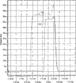
Fig. 3 shows before the locking condition source among the prior art DLL shown in Figure 2 and converges the curve chart of electric current.Source electric current by transistor 210 among track 150 and Fig. 2 is corresponding, and the remittance electric current that passes through transistor 215 among track 152 and Fig. 2 is corresponding.Before locking condition, the source electric current and the electric current that converges are unequal, and the source electric current is greater than converging electric current.In locking condition, each track 150 is identical with the area of 152 belows.Therefore, when electric current was unequal, DLL had compensated phase error or " static phase error ", so that keep identical electric charge at node OUT.Phase error is derived from: the signal with reduced-current is wideer than the signal with high current in time, makes area equal in fact.Although the trailing edge of each track 150 and 152 appears in the place in the approximately uniform time, at different time places rising edge appears, to compensate unequal source and to converge electric current.Therefore, the design of the essence of prior art DLL has caused phase error.
In submicron technology (that is, 0.13 micron or littler), transistorized output impedance reduces along with the shortening of channel length, so transistor does not satisfy the requirement of the required output impedance of the output transistor of charge pump.A kind of output impedance that improves charge pump is so that the minimized known method of static phase error is by using the cascode amplifier current source.Yet the cascode amplifier current source does not meet the development trend that supply voltage reduces.For example, for the supply voltage of 1V and the typical 0.25V threshold voltage to 0.3V, the 1V supply voltage is low excessively, can not keep the cascode amplifier current source (each has two threshold voltages) of two series connection.
Summary of the invention
By using (active) current source initiatively to come static phase error in the minimum charge pump.The influence that the active current source has also alleviated low supply voltage.According to embodiments of the invention, a kind of charge pump comprises pull-up circuit, pull-down circuit and operational amplifier.Pull-up circuit provides pull-up current to improve the voltage of charge pump output place.Pull-down circuit provides pull-down current to reduce the voltage of charge pump output place.Operational amplifier has first input and second input.First input links to each other with charge pump output, and second imports and pull down circuit and provide the transistor drain of electric current to link to each other.Operational amplifier output links to each other with pull-down circuit with described transistor.Operational amplifier is adjusted the voltage level of operational amplifier output place, so that the voltage difference minimum between the operational amplifier input, and reduces poor between pull-down current and the pull-up current.
Charge pump can also comprise first start-up circuit that links to each other of input with operational amplifier, and during the powering up of charge pump, described start-up circuit is made as the voltage level that is lower than supply voltage with the voltage of first input.In an embodiment of the present invention, the supply voltage that provides to charge pump can be about 1 volt.
Pull-up circuit comprises a PMOS device and the 2nd PMOS device.The drain electrode of the one PMOS device links to each other with the source electrode of the 2nd PMOS device, and the source electrode of a PMOS device links to each other with supply voltage node (or rail (rail)), and the drain electrode of the 2nd PMOS device links to each other with charge pump output.When a PMOS break-over of device, pull-up circuit provides pull-up current.
Pull-down circuit comprises first nmos device and second nmos device.The drain electrode of first nmos device links to each other with the source electrode of second nmos device, and the source electrode of first nmos device links to each other with ground, and the drain electrode of second nmos device links to each other with charge pump output.When the first nmos device conducting, pull-down circuit provides pull-down current.
Charge pump also comprises and pulls down the reference current source that circuit and pull-up circuit provide electric current.In one embodiment, reference current source comprises programmable transistor array.Operational amplifier can be the input of low-power rail-to-rail, rail-to-rail output operational amplifier.
Description of drawings
Shown in accompanying drawing (wherein run through different accompanying drawings and represent same parts) by same numeral, to describe more specifically according to the following of the embodiment of the invention, above and other objects of the present invention, feature and advantage will be more apparent.It is pro rata that accompanying drawing needs not to be, but focus on demonstration principle of the present invention.
Fig. 1 is the block diagram of prior art delay lock loop;
Fig. 2 is the schematic diagram of the prior art charge pump that can use in prior art DLL shown in Figure 1;
Fig. 3 shows the curve chart at source in prior art DLL shown in Figure 2 before the locking condition and remittance electric current;
Fig. 4 is the schematic diagram of charge pump in accordance with the principles of the present invention;
Fig. 5 shows before the locking condition source in the charge pump shown in Figure 4 and converges the curve chart of current impulse;
Fig. 6 is the schematic diagram of operational amplifier shown in Figure 4;
Fig. 7 is the schematic diagram of the programmable transistor array that can use in the charge pump of Fig. 4;
Fig. 8 is the block diagram that can use the prior art phase-locked loop of charge pump; And
Fig. 9 shows the schematic diagram of another embodiment of charge pump with different configurations, wherein the nmos device shown in the embodiment among operational amplifier control PMOS device rather than Fig. 4.
Embodiment
Being described below of the preferred embodiment of the present invention.
Fig. 4 is the schematic diagram of charge pump 300 in accordance with the principles of the present invention.Charge pump 300 comprises a plurality of transistors.In an illustrated embodiment, transistor is metal-oxide semiconductor (MOS) (" MOS ") transistor, also is known as field-effect transistor (" FET ").As known to those skilled in the art, there is two types MOS transistor: n channel MOS transistor (NMOS) and p channel MOS transistor (PMOS).Charge pump 300 comprises NOMS transistor and PMOS transistor.Utilize the circle at grid place to show the PMOS transistor graphically.
Current mirror M1 comprises bias PMOS transistor 314 and nmos pass transistor 310 and 312.Voltage V
BnThe bias voltage of current mirror M1 is set, and the electric current of the PMOS transistor 314 of flowing through is set. PMOS transistor 314 and 313 provides the reference current source that electric current is offered pull-down circuit and pull-up circuit.Mirror image is by the electric current of PMOS transistor 314 in PMOS transistor 312 and 310.As the common practise of this area,, can revise each transistorized electric current in the current mirror of flowing through by changing these size of devices (width/height ratio).
Depend on bias voltage V by the source electrode-drain electrode connected node place of PMOS device 314
BnThe voltage that provides, the PMOS device 314 among the current mirror M1 provides initial current to charge pump.When using charge pump in the DLL system, bias voltage is adjusted the maximum current of charge pump according to the total delay of delay chain, and is constant so that the ratio between reference frequency and the DLL bandwidth keeps.
The grid of PMOS transistor 314 links to each other with the drain electrode of PMOS transistor 314.PMOS device 312 links to each other with the grid of PMOS device 314 with 310 grid, and this makes it possible to this initial current is mirrored to PMOS transistor 312 and 310.The drain electrode of nmos pass transistor 316 links to each other with the drain electrode of PMOS device 312.Therefore, the electric current that is mirrored to PMOS device 312 is the same current that is provided to nmos device 316 among the current mirror M3.The grid of nmos device 316 links to each other with the grid of nmos device 315, and this makes it possible to drain current with nmos device 316 and is mirrored to nmos device 315 among the current mirror M3, so that pull-down current is provided.
Usually, when enabling charge pump (assert signal ENABLE or be driven to logical one) and asserting signal UP, by by NAND door 301, inverter 302 and 304 and transmission gate (pass gate) 303 voltage that is applied to the grid of transistor 309 come " conducting " transistor 309.This allows flow through PMOS transistor 309 and 310 in the pull-up circuit of electric current.This electric current adds electric charge to the OUT node that links to each other with ring wave filter 206 (Fig. 1).This has increased electric charge, transistor 309 is in the voltage increase that " conducting " causes node OUT simultaneously, when by the charge pump 105 shown in the charge pump 300 replacements prior art DLL 100 shown in Figure 1, this causes having increased the delay that is produced by voltage controlled delay line 102.Similarly, when enabling charge pump (ENABLE height) and asserting signal DOWN, come " conducting " transistor 317 by the voltage that is applied to grid by NAND door 305 and inverter 306,307 and 308.This allows flow through transistor 315 and 317 in the pull-down circuit of electric current.Electric current flows to ground by transistor 315,317 from node OUT, and this electric current is taken electric charge away from node OUT.This has reduced electric charge, and transistor 315 is in the voltage decline that " conducting " causes node OUT simultaneously, and the delay that is produced by voltage controlled delay line 102 (Fig. 1) reduces.
Coupling is passed through inverter 303,304 and is passed through the path of inverter 307,308 to the grid of transistor 310,315 from the UP/DOWN signal of the input of NAND door 302,304, postpones so that identical insertion to be provided.Comprise transmission gate 303 in the path so that be replicated in from the DOWN signal to transistor the delay that the inverter 307 the path of 317 grid is increased.In order to compensate the small electric pressure drop at the source-drain path two ends of nmos pass transistor 309 when transistor 309 " conducting ", add PMOS transistor 311 and 313, so that the symmetry with current path by PMOS transistor 309 to be provided.Nmos pass transistor 318 provides the symmetry with the current path that passes through PMOS transistor 315.
Current mirror M3 control pull-down current (arriving ground by nmos pass transistor 315) and pull-up current are (from V
DdBy PMOS transistor 310) between ratio.Pull-down current has reduced the voltage at node OUT place, and pull-up current has increased the voltage at node OUT place.Therefore, the M1 current mirror is provided with the maximum current of charge pump by PMOS device 310, draw in the control of M3 current mirror and pull-down current between ratio.By using known technology, current mirror M1 and M3 can adjust or be able to programme.Can determine the size of transistor 315 among the current mirror M3 and 316, so that transmit more or less electric current.This allows circuit designers to compensate other factor that for example dead resistance and electric capacity and parameter change.Yet this adjustment is static, in case packaged chip just can not be readjusted, and can not compensate the variation of OUT voltages at nodes.
According to one embodiment of present invention, as shown in Figure 4, provide the active adjustment of current mirror by using operational amplifier.Initiatively the anti-phase input of the operational amplifier 323 among the current mirror M3 links to each other with node OUT, and the noninverting input of operational amplifier 323 links to each other with node " n14 ".The output node of operational amplifier 323 links to each other with the grid of node " ctrl " with nmos device 315,316.If between node OUT and " n14 ", exist free voltage poor, the voltage that operational amplifier 323 is adjusted on the Control Node " ctrl ".By nmos device 315,316, the change in voltage on the Control Node " ctrl " causes the corresponding voltage on node OUT and the node " n14 " to change.
In the operating period of charge pump, operational amplifier 323 equals output voltage on the node OUT in fact by keeping voltage on the node " n14 " on one's own initiative, makes the static phase error minimum.When DLL is in the lock state, output (" OUT ") locate to produce draw with pull-down current on identical extremely important.In the DLL that has realized locking condition, when UP and DOWN pulse had the equal duration, most of times can not be carried out charge or discharge to node OUT on one's own initiative.In addition, UP and DOWN pulse can have than in conjunction with the short duration of the described prior art charge pump of Fig. 2, and this causes reducing of power demand in the device.Therefore, the voltage at node OUT place keeps constant in fact.The change in voltage that node " ctrl " is located causes the respective change of electric current mobile in nmos pass transistor 315,316.Yet, because the electric capacity of node " n14 " is less than the electric capacity of node OUT place appearance, the variation that node " ctrl " is located voltage to the influence of node " n14 " faster than influence to node OUT.
The voltage at the operational amplifier 323 following OUT of Control Node on one's own initiative places: if the voltage that node " n14 " is located is higher than the voltage at node OUT place, then operational amplifier 323 increases the voltage that node " ctrl " is located.The increase that node " ctrl " is located voltage cause the flowing through electric current of nmos pass transistor 316 and nmos pass transistor 315 increases, and this has reduced the voltage that node " n14 " is located, and is identical with the voltage at node OUT place up to this voltage.If the voltage of node " n14 " is less than the voltage of node OUT, then operational amplifier 323 reduces the voltage of node " ctrl ".What node " ctrl " was gone up voltage reduces to cause reducing of the electric current that flows in nmos pass transistor 316 and nmos pass transistor 315.Because the voltage on the voltage that node " ctrl " the is located change node " n14 " is faster than the voltage that changes on the node OUT, the voltage on node " n14 " equals the voltage on the node OUT, has reached new balance point.When the voltage on the node " n14 " was identical in fact with output voltage OUT, the source/drain current (pull-down current) by nmos device 315 equated with source/drain current (pull-up current) by PMOS device 310 in fact.
By the active current mirror that comprises operational amplifier is provided to charge pump, nmos pass transistor to 315,316 and the PMOS transistor equal in fact to the voltage conditions at 312,310 drain electrode, source electrode and grid place, and near many, this causes point-device matching current by nmos pass transistor 315 and PMOS transistor 310 than prior art circuits shown in Figure 2. Transistor 319 and 320 is simple buffer capacitors, and this has prevented to be connected to by the noise that nmos device 315 and PMOS device 310 cause each bias node of current mirror M1, M2.
Preferably, operational amplifier 323 has rail-to-rail (rail to rail) (Vdd to Vss ()) input range.At transistor the 315, the 316th, among the embodiment of nmos device as shown in Figure 4, required output area from Vdd down to the predetermined voltage more than closely, that is, and than a threshold voltage (Vtn) of the high nmos pass transistor in ground.This output voltage range has guaranteed that complete " the ending " that causes circuit to move appears in nmos pass transistor 315 and 316 never.At transistor the 315, the 316th, among the optional embodiment of PMOS device as shown in Figure 9, required output area is (that is, than the low transistorized threshold voltage of PMOS of Vdd) from Vss to Vtp.Therefore, the operational amplifier 323 with rail-to-rail output area is preferred.
During powering up the stage, if the voltage that node " n14 " is located is lower than the voltage at node OUT place, with output (being node " the ctrl ") step-down of operational amplifier.Because node " ctrl " links to each other with the grid of nmos device 315, nmos device 315 " ends " probably.Circuit may be frozen in this state, maybe may need the long period to recover.Both of these case all is undesirable.
The start-up circuit that comprises nmos device 321 and nmos device 322 helps charge pump to reach its working point in the stage of powering up.Start-up circuit is made as the voltage of node OUT less than V at first
DdNumerical value.This makes operational amplifier 323 correctly to operate after powering up the stage.The enabling signal of asserting in the predetermined amount of time that powers up after powering up in the stage links to each other with the grid of nmos device 322.The nmos device 322 diode connected mode that to be grids link to each other with node OUT with source electrode.The drain electrode of nmos device 322 links to each other with the drain electrode of nmos device 322.
When asserting with enabling signal that the drain electrode of nmos device 321 links to each other, nmos device 322 " conducting ".Node OUT is approximately equal to V
Dd, therefore, because nmos device 321 and nmos device 322 " conducting ", the electric current of flow through nmos device 321 and nmos device 322 causes node OUT place voltage to descend.
Therefore, start-up circuit has guaranteed the voltage located less than node " n14 " at the voltage that powers up stage node OUT place, therefore, initial difference input voltage to operational amplifier 323 is for just, and the startup stage during, the output place node " ctrl " of operational amplifier 323 is driven to high, keep nmos device 315 conductings.This forces node OUT to be approximately the threshold voltage of nmos pass transistor in this predetermined amount of time.After powering up the stage, going to assert (de-assert) enabling signal no longer needs to enable start-up circuit.
The present invention is reduced to about 4% with current deviation (that is the difference between current between nmos pass transistor 315 and the PMOS transistor 310).This causes having reduced static phase error for whole DLL system than the highland.In the present embodiment by the current deviation of charge pump is reduced to 4% from 20%, the whole static phase error of PLL/DLL is reduced to 60ps from 300ps.
Fig. 5 shows before the locking condition source in the charge pump shown in Figure 4 and converges the curve chart of current impulse.In this example, track 154 is with corresponding by the source electric current of transistor 309 among Fig. 4, and track 156 is with corresponding by the remittance electric current of transistor 317 among Fig. 4.In an embodiment according to the present invention, the source electric current is equal in fact on amplitude with the electric current that converges.Because Fig. 5 shows the pulse before the locking condition, DLL can begin to change the voltage of node OUT, so that the edge of align when the search lock condition source and remittance pulse.When reaching locking condition, the area of each track 154,156 below equates that this causes the stable level of node OUT place voltage.When the source equated in fact on amplitude with the remittance electric current, the alignment of porch was more accurate, has eliminated one of largest component that static phase error is worked.
Fig. 6 is the schematic diagram of the embodiment of operational amplifier 323 shown in Figure 4.Operational amplifier is right based on the complementation input with the very low voltage operation.In an illustrated embodiment, operational amplifier can utilize the 1V general supply voltage from Vdd to Vss to operate, and supposes that wherein Vss is about 0V (linking to each other with ground).
Output stage 440 comprises transistor 401 and 402.Biasing circuit comprises transistor 414,415,416,417,418 and 419, and the transistor 403 in the transistor in output stage 440 401, first differential amplifier 442 and the transistor 413 in second differential amplifier 444 provide bias voltage.
Node OUT shown in Figure 4 links to each other with the difference of each differential amplifier input " inm ", and node shown in Figure 4 " n14 " links to each other with the difference input " inp " of each differential amplifier.The output stage of operational amplifier " diff_out " links to each other with node " ctrl " shown in Figure 4.
When enabling charge pump 300 (Fig. 4) (assert signal ENABLE or be driven to logical one), transistor 419 conductings make the electric current transistor 416,417,418 and 419 of can flowing through.The electric current in the transistor 409 in mirror image second differential amplifier 444 in transistor 408.Transistor 408 provides the output of second differential amplifier.In the transistor 406 of first differential amplifier 440, to suing for peace and be mirrored to transistor 402 in the output stage from the electric current (representing the output of first differential amplifier) of transistor 404 with from the electric current (representing the output of second differential amplifier) of transistor 408.When forbidding charge pump 300 (go to assert signal ENABLE or be driven to logical zero), because the logical zero at transistor 419 grid places, transistor 419 ends, and operational amplifier can not be revised the voltage on the ctrl node.
Other embodiment can use the programmable array main transistor to be used for the reference current source of current mirror, so that the operation of configuration or test circuit.Fig. 7 is the schematic diagram 500 that is suitable for replacing this programmable transistor array of the transistor 313 of Fig. 4 and transistor 314.Four effectively low selects signals (SEL0b, SEL1b, SEL2b and SEL3b) to select PMOS transistors 501,502,503 to link to each other with 504 with four.Each selects the different current mirror master PMOS transistor of transistor AND gate 505,506,507 to link to each other with 508.One or more SEL signals are for effectively low, and this makes it possible to the variable current that flows.The changes in amplitude of electric current depends on the number that is in effectively low SEL signal.For example, when only SEL0b is effectively low, can only flow through PMOS transistor 505 and select transistor 501 of electric current, and in the transistor 312 and 310 of Fig. 4 this electric current of mirror image.Selecting signals at all four be when effectively hanging down, and the PMOS transistor 505,506,507 and 508 and all selection transistors because electric current is flowed through has increased the amplitude of electric current.By the V that links to each other with 312 with transistor 310
BnNode is this electric current of mirror image in transistor 312 and 310.
Can control the SEL signal by other any known technology of register, fusing programming, masked edit program or this area.Although show four groups of main transistors able to programme, can use arbitrary number.Two transistors 416 and 418 by replaced Fig. 4 by transistorized programmable array can be used to the similar circuit of utilizing nmos pass transistor add programmability.
The charge pump that the present invention is not limited to use in DLL.For example, the present invention can also be used in the charge pump in the phase-locked loop.Phase-locked loop (PLL) is the another kind of known circuits that is used for first clock signal and second clock signal Synchronization.
Fig. 8 is the block diagram of prior art PLL 600.Cushion the clock (CLK) that provides from the outside by clock buffer 601, so that the reference clock that links to each other with phase detectors 604 (CLK_REF) is provided.According to the phase difference between CLK_REF and the CLK_FB, phase detectors 604 produce phase control signal (UP, DOWN).
The phase control signal (UP/DOWN) of charge pump 605 and 606 pairs of phase detectors 604 of ring wave filter carries out integration, so that variable bias voltage V to be provided
CTRL110.Bias voltage V
CTRLControl voltage controlled oscillator (VCO) 602, voltage controlled oscillator 602 clock signal CLK_OUT.The frequency of clock signal CLK_OUT and bias voltage V
CTRL610 are directly proportional.VCO is well known in the art.
Alternatively, the CLK_OUT signal is linked to each other with voltage divider 603, to produce feedback clock signal CLK_FB.If phase detectors detected the rising edge of CLK_REF before the rising edge of CLK_FB, then assert to cause V by the UP signal
CTRLRaise, thus the frequency of increase CLK_OUT signal.If phase detectors detected the rising edge of CLK_FB before the rising edge of CLK_REF, then assert to cause V by the DOWN signal
CTRLReduce, thereby reduce the frequency of CLK_OUT signal.
Fig. 9 shows the schematic diagram of another embodiment of charge pump with different configurations, wherein the NOMS transistor shown in the embodiment among operational amplifier control PMOS device rather than Fig. 4.By using same principle of the present invention, operational amplifier 323 according to in conjunction with described identical mode embodiment illustrated in fig. 4, balanced transistor 310 ', 312 ', 315 and 316 ' drain electrode.
The present invention has been described, for use in the charge pump in the PLL/DLL system.Yet the present invention is not limited to the PLL/DLL system.Can in can not reaching any system of ground (this causes, and op amp can not move in the current mirror initiatively), the output voltage of point-device current mirror of needs and current mirror use the present invention.
Although illustrate and described the present invention particularly with reference to preferred embodiment, those skilled in the art will appreciate that under the prerequisite that does not break away from the scope of the present invention that is defined by the following claims, can carry out various changes to form and details.
Claims (13)
1. charge pump comprises:
Pull-up circuit provides pull-up current to improve the voltage of charge pump output place;
Pull-down circuit provides pull-down current to reduce the voltage of charge pump output place;
Operational amplifier, have first input and second input, first input links to each other with charge pump output, second input with pull down circuit and provide the transistor drain of electric current to link to each other, operational amplifier output links to each other with described transistorized grid with pull-down circuit, voltage difference between operational amplifier is imported according to second input and first is adjusted the voltage level of operational amplifier output place, so that the voltage difference minimum between second input and first input, and reduce the poor of pull-down current and pull-up current; And
With first start-up circuit that link to each other of input, during the powering up of charge pump, described start-up circuit is made as the voltage level that is lower than supply voltage with the voltage of first input.
2. charge pump according to claim 1, wherein, the supply voltage that provides to charge pump is 1 volt.
3. charge pump according to claim 1, wherein, pull-up circuit comprises a PMOS device and the 2nd PMOS device, the drain electrode of the one PMOS device links to each other with the source electrode of the 2nd PMOS device, the source electrode of the one PMOS device links to each other with the supply voltage node, and the output of the drain electrode of the 2nd PMOS device and charge pump links to each other, and when a PMOS break-over of device, pull-up circuit provides pull-up current.
4. charge pump according to claim 1, wherein, pull-down circuit comprises first nmos device and second nmos device, the drain electrode of first nmos device links to each other with the source electrode of second nmos device, the source electrode of first nmos device links to each other with ground, and the output of the drain electrode of second nmos device and charge pump links to each other, and when the first nmos device conducting, pull-down circuit provides pull-down current.
5. charge pump according to claim 1 also comprises:
Pulling down circuit and pull-up circuit provides the reference current source of electric current.
6. charge pump according to claim 5, wherein, reference current source comprises programmable transistor array.
7. charge pump according to claim 1, wherein, operational amplifier has the output area of the input range and the rail-to-rail of rail-to-rail.
8. charge pump according to claim 6, wherein, pull-up circuit comprises a PMOS device and the 2nd PMOS device, the drain electrode of the one PMOS device links to each other with the source electrode of the 2nd PMOS device, the source electrode of the one PMOS device links to each other with the supply voltage node, and the output of the drain electrode of the 2nd PMOS device and charge pump links to each other, and when a PMOS break-over of device, pull-up circuit provides pull-up current.
9. charge pump according to claim 6, wherein, pull-down circuit comprises first nmos device and second nmos device, the drain electrode of first nmos device links to each other with the source electrode of second nmos device, the source electrode of first nmos device links to each other with ground, and the output of the drain electrode of second nmos device and charge pump links to each other, and when the first nmos device conducting, pull-down circuit provides pull-down current.
10. charge pump according to claim 6, wherein, operational amplifier has the output area of the input range and the rail-to-rail of rail-to-rail.
11. a method that is used for making the deviation electric current minimum of charge pump comprises:
The voltage of pull-up current with output place of raising charge pump is provided, and provides pull-down current to reduce the voltage of charge pump output place;
First input of operational amplifier is linked to each other with charge pump output;
Provide the transistor drain of electric current to link to each other with pulling down circuit second input of operational amplifier,
Operational amplifier output is linked to each other with described transistorized grid with pull-down circuit;
During the powering up of charge pump, the voltage of first input is set to be lower than the voltage level of supply voltage; And
Adjust the voltage level of operational amplifier output place according to the voltage difference between second input and first input, so that the voltage difference minimum between second input and first input, and reduce the poor of pull-up current and pull-down current.
12. method according to claim 11, wherein, supply voltage is 1 volt.
13. a charge pump comprises:
Be used to provide the device of the voltage of pull-up current to improve charge pump output place;
Be used to provide the device of the voltage of pull-down current to reduce charge pump output place;
Amplifying device, have first input and second input, first input links to each other with charge pump output, second the input with to being used to provide the device of pull-down current to provide the transistor drain of electric current to link to each other, amplifying device is exported and is used to provide the device of pull-down current to link to each other with described transistorized grid, amplifying device is adjusted the voltage level of amplifying device output place according to the voltage difference between second input and first input, so that the voltage difference minimum between second input and first input, and reduce the poor of pull-down current and pull-up current; And
Be used for during the powering up of charge pump, the voltage of first input being made as the device of the voltage level that is lower than supply voltage.
Priority Applications (1)
| Application Number | Priority Date | Filing Date | Title |
|---|---|---|---|
| CN200910204669.1A CN101677244B (en) | 2003-12-11 | 2004-12-10 | High output impedance charge pump for PLL/DLL |
Applications Claiming Priority (2)
| Application Number | Priority Date | Filing Date | Title |
|---|---|---|---|
| US52895803P | 2003-12-11 | 2003-12-11 | |
| US60/528,958 | 2003-12-11 |
Related Child Applications (1)
| Application Number | Title | Priority Date | Filing Date |
|---|---|---|---|
| CN200910204669.1A Division CN101677244B (en) | 2003-12-11 | 2004-12-10 | High output impedance charge pump for PLL/DLL |
Publications (2)
| Publication Number | Publication Date |
|---|---|
| CN1902823A CN1902823A (en) | 2007-01-24 |
| CN100593908C true CN100593908C (en) | 2010-03-10 |
Family
ID=34676868
Family Applications (2)
| Application Number | Title | Priority Date | Filing Date |
|---|---|---|---|
| CN200480037036A Active CN100593908C (en) | 2003-12-11 | 2004-12-10 | High output impedance charge pump for PLL/DLL |
| CN200910204669.1A Active CN101677244B (en) | 2003-12-11 | 2004-12-10 | High output impedance charge pump for PLL/DLL |
Family Applications After (1)
| Application Number | Title | Priority Date | Filing Date |
|---|---|---|---|
| CN200910204669.1A Active CN101677244B (en) | 2003-12-11 | 2004-12-10 | High output impedance charge pump for PLL/DLL |
Country Status (6)
| Country | Link |
|---|---|
| US (9) | US7176733B2 (en) |
| EP (2) | EP3512102B1 (en) |
| JP (2) | JP4914219B2 (en) |
| KR (3) | KR100968296B1 (en) |
| CN (2) | CN100593908C (en) |
| WO (1) | WO2005057791A1 (en) |
Families Citing this family (50)
| Publication number | Priority date | Publication date | Assignee | Title |
|---|---|---|---|---|
| WO2005057791A1 (en) * | 2003-12-11 | 2005-06-23 | Mosaid Technologies Incorporated | High output impedance charge pump for pll/dll |
| JP4249042B2 (en) * | 2004-01-22 | 2009-04-02 | 三菱電機株式会社 | Offset cancel device for differential charge pump |
| US7382178B2 (en) * | 2004-07-09 | 2008-06-03 | Mosaid Technologies Corporation | Systems and methods for minimizing static leakage of an integrated circuit |
| US7102400B1 (en) * | 2004-08-30 | 2006-09-05 | Sitel Semiconductor B.V. | Phase locked loop charge pump and method of operation |
| US7236018B1 (en) * | 2004-09-08 | 2007-06-26 | Altera Corporation | Programmable low-voltage differential signaling output driver |
| US7141936B2 (en) * | 2004-11-10 | 2006-11-28 | Xerox Corporation | Driving circuit for light emitting diode |
| US7750695B2 (en) * | 2004-12-13 | 2010-07-06 | Mosaid Technologies Incorporated | Phase-locked loop circuitry using charge pumps with current mirror circuitry |
| US7190201B2 (en) * | 2005-02-03 | 2007-03-13 | Mosaid Technologies, Inc. | Method and apparatus for initializing a delay locked loop |
| ATE449483T1 (en) * | 2005-06-29 | 2009-12-15 | Nxp Bv | SYNCHRONIZATION SCHEME WITH ADAPTIVE REFERENCE FREQUENCY CORRECTION |
| US7567133B2 (en) * | 2006-04-06 | 2009-07-28 | Mosaid Technologies Corporation | Phase-locked loop filter capacitance with a drag current |
| JP2007295180A (en) * | 2006-04-24 | 2007-11-08 | Kawasaki Microelectronics Kk | Charge pump circuit, and pll circuit and dll circuit using same |
| KR100843200B1 (en) * | 2006-08-22 | 2008-07-02 | 삼성전자주식회사 | Adaptive bandwidth PLL with current boosting circuit |
| US7915933B2 (en) * | 2006-11-30 | 2011-03-29 | Mosaid Technologies Incorporated | Circuit for clamping current in a charge pump |
| TWI361568B (en) | 2007-01-30 | 2012-04-01 | Mosaid Technologies Inc | Delay-locked loop and a method for providing charge signal to a charge pump of the same |
| US7511580B2 (en) * | 2007-03-25 | 2009-03-31 | Smartech Worldwide Limited | Charge pump circuit with dynamic current biasing for phase locked loop |
| US20080303565A1 (en) * | 2007-06-08 | 2008-12-11 | Yen-Hsun Hsu | Dll circuit and related method for avoiding stuck state and harmonic locking utilizing a frequency divider and an inverter |
| US7583116B2 (en) * | 2007-08-03 | 2009-09-01 | International Business Machines Corporation | High output resistance, wide swing charge pump |
| US7701270B2 (en) * | 2007-08-03 | 2010-04-20 | International Business Machines Corporation | Structure for a high output resistance, wide swing charge pump |
| US7771115B2 (en) * | 2007-08-16 | 2010-08-10 | Micron Technology, Inc. | Temperature sensor circuit, device, system, and method |
| US7977984B1 (en) * | 2007-10-13 | 2011-07-12 | Altera Corporation | High-speed charge pump circuits |
| US8018269B2 (en) * | 2007-11-13 | 2011-09-13 | Qualcomm Incorporated | Fast-switching low-noise charge pump |
| JP5092770B2 (en) * | 2008-01-29 | 2012-12-05 | 富士通セミコンダクター株式会社 | Phase lock loop circuit and delay lock loop circuit |
| US7705649B1 (en) * | 2008-04-03 | 2010-04-27 | National Semiconductor Corporation | Duty cycle correction circuit with small duty error and wide frequency range |
| CN101488710B (en) * | 2008-10-22 | 2012-06-13 | 成都国腾电子技术股份有限公司 | A charge pump circuit |
| JP2010239554A (en) * | 2009-03-31 | 2010-10-21 | Nec Corp | Charge pump, frequency synthesizer and control method |
| US7965117B2 (en) * | 2009-05-06 | 2011-06-21 | Freescale Semiconductor, Inc. | Charge pump for phase locked loop |
| US20100308899A1 (en) * | 2009-06-04 | 2010-12-09 | Pericom Semiconductor Corp. | Dual-Output Triple-Vdd Charge Pump |
| CN101572481B (en) * | 2009-06-11 | 2014-03-26 | 四川和芯微电子股份有限公司 | Charge pump circuit |
| US8525564B2 (en) * | 2010-10-20 | 2013-09-03 | University Of Southern California | Charge-based phase locked loop charge pump |
| US8400199B2 (en) | 2010-11-26 | 2013-03-19 | Mediatek Inc. | Charge pump, phase frequency detector and charge pump methods |
| US8378725B2 (en) | 2011-03-14 | 2013-02-19 | Freescale Semiconductor, Inc. | Adaptive bandwidth phase-locked loop |
| US8427210B2 (en) * | 2011-07-26 | 2013-04-23 | United Microelectronics Corp. | Charge pump |
| US8368442B1 (en) * | 2011-08-15 | 2013-02-05 | United Microelectronics Corp. | Charge pump |
| TWI451700B (en) * | 2011-12-05 | 2014-09-01 | Global Unichip Corp | Clock and data recovery circuit |
| US8432200B1 (en) | 2012-01-05 | 2013-04-30 | Freescale Semiconductor, Inc. | Self-tracking adaptive bandwidth phase-locked loop |
| US8432201B1 (en) * | 2012-05-19 | 2013-04-30 | Freescale Semiconductor, Inc. | Phase-locked loop (PLL) circuit |
| TWI499215B (en) * | 2012-10-17 | 2015-09-01 | Mstar Semiconductor Inc | Charging/discharging circuit and pll utilizing the charging/discharging circuit |
| US8760202B1 (en) | 2013-05-15 | 2014-06-24 | Freescale Semiconductor, Inc. | System for generating clock signal |
| CN103346784B (en) * | 2013-06-18 | 2016-04-13 | 成都嘉纳海威科技有限责任公司 | A kind of matching type charge pump circuit for phase-locked loop |
| CN103368565A (en) * | 2013-07-10 | 2013-10-23 | 成都锐成芯微科技有限责任公司 | Frequency-limited voltage-controlled oscillator |
| KR102081394B1 (en) * | 2013-12-30 | 2020-02-26 | 에스케이하이닉스 주식회사 | Semiconductor apparatus |
| US20150200588A1 (en) * | 2014-01-16 | 2015-07-16 | Qualcomm Incorporated | Low-power, self-biasing-capable charge pump with current matching capabilities |
| TWI547097B (en) * | 2014-07-24 | 2016-08-21 | 登豐微電子股份有限公司 | Delay circuit |
| CN104811189A (en) * | 2015-05-14 | 2015-07-29 | 东南大学 | Charge pump circuit in charge pump phase-locked loop |
| US9634561B1 (en) | 2016-01-07 | 2017-04-25 | Freescale Semiconductor, Inc. | Programmable charge pump |
| US9991896B2 (en) * | 2016-08-09 | 2018-06-05 | Synopsys, Inc. | Phase locked loop circuit with charge pump up-down current mismatch adjustment and static phase error reduction |
| CN108448891A (en) * | 2018-04-23 | 2018-08-24 | 电子科技大学 | A kind of regulator circuit based on charge pump construction |
| US10496127B1 (en) * | 2018-06-04 | 2019-12-03 | Linear Technology Holding Llc | Multi-chip timing alignment to a common reference signal |
| US10623007B1 (en) | 2019-01-08 | 2020-04-14 | Apple Inc. | Energy-efficient charge pump design for phase-locked loops |
| US11545984B2 (en) * | 2020-06-10 | 2023-01-03 | Sandisk Technologies Llc | Charge pump with wide current range |
Family Cites Families (86)
| Publication number | Priority date | Publication date | Assignee | Title |
|---|---|---|---|---|
| GB8329511D0 (en) * | 1983-11-04 | 1983-12-07 | Inmos Ltd | Timing apparatus |
| KR940011436B1 (en) | 1989-04-19 | 1994-12-15 | 가부시끼가이샤 히다찌세이사꾸쇼 | Magnetic disk memory apparatus |
| GB2249443B (en) * | 1990-10-31 | 1994-06-08 | Gen Electric Co Plc | Charge pump circuit |
| US5233314A (en) | 1992-03-27 | 1993-08-03 | Cyrix Corporation | Integrated charge-pump phase-locked loop circuit |
| US5362990A (en) | 1993-06-02 | 1994-11-08 | Motorola, Inc. | Charge pump with a programmable pump current and system |
| JPH0818414A (en) * | 1994-04-26 | 1996-01-19 | Hitachi Ltd | Delay circuit for signal processing |
| US5796673A (en) | 1994-10-06 | 1998-08-18 | Mosaid Technologies Incorporated | Delay locked loop implementation in a synchronous dynamic random access memory |
| US5473283A (en) | 1994-11-07 | 1995-12-05 | National Semiconductor Corporation | Cascode switched charge pump circuit |
| GB2339638B (en) * | 1995-04-11 | 2000-03-22 | Int Rectifier Corp | Charge pump circuit for high side switch |
| KR970008906A (en) | 1995-07-18 | 1997-02-24 | 가네꼬 히사시 | PLL circuit |
| JP3446425B2 (en) * | 1995-10-20 | 2003-09-16 | 三菱電機株式会社 | Frequency synchronization circuit |
| JP2845185B2 (en) * | 1995-11-29 | 1999-01-13 | 日本電気株式会社 | PLL circuit |
| US5604694A (en) * | 1996-01-16 | 1997-02-18 | Vlsi Technology, Inc. | Charge pump addressing |
| JPH09331250A (en) * | 1996-06-12 | 1997-12-22 | Fujitsu Ltd | Charge pump circuit and pll frequency synthesizer |
| EP0837558A1 (en) * | 1996-10-18 | 1998-04-22 | Hewlett-Packard Company | A CMOS op-amp input stage with constant small signal gain from rail-to-rail |
| US5831484A (en) | 1997-03-18 | 1998-11-03 | International Business Machines Corporation | Differential charge pump for phase locked loop circuits |
| GB2324423B (en) | 1997-04-16 | 1999-07-21 | Lsi Logic Corp | Charge pump |
| CA2204089C (en) | 1997-04-30 | 2001-08-07 | Mosaid Technologies Incorporated | Digital delay locked loop |
| JPH118553A (en) * | 1997-06-16 | 1999-01-12 | Hitachi Ltd | Pll circuit and semiconductor integrated circuit |
| US5933037A (en) * | 1997-08-29 | 1999-08-03 | Adaptec, Inc. | High speed phase lock loop having constant bandwidth |
| US5945855A (en) | 1997-08-29 | 1999-08-31 | Adaptec, Inc. | High speed phase lock loop having high precision charge pump with error cancellation |
| US6124755A (en) * | 1997-09-29 | 2000-09-26 | Intel Corporation | Method and apparatus for biasing a charge pump |
| US5939949A (en) | 1998-03-16 | 1999-08-17 | National Semiconductor Corporation | Self-adjusting startup control for charge pump current source in phase locked loop |
| KR19990080026A (en) * | 1998-04-11 | 1999-11-05 | 윤종용 | Charge pump in phase locked loop circuit |
| US6172571B1 (en) | 1998-07-28 | 2001-01-09 | Cypress Semiconductor Corp. | Method for reducing static phase offset in a PLL |
| KR100555471B1 (en) * | 1998-07-29 | 2006-03-03 | 삼성전자주식회사 | Charge pump adaptively controlling current offset |
| US6329872B1 (en) | 1998-08-14 | 2001-12-11 | Nortel Networks Limited | Charge pump circuit for a phase locked loop |
| US6181210B1 (en) | 1998-09-21 | 2001-01-30 | Broadcom Corporation | Low offset and low glitch energy charge pump for PLL-based timing recovery systems |
| US6369624B1 (en) | 1998-11-03 | 2002-04-09 | Altera Corporation | Programmable phase shift circuitry |
| US6163184A (en) | 1998-12-09 | 2000-12-19 | Lucent Technologies, Inc. | Phase locked loop (PLL) circuit |
| US20020041196A1 (en) | 1999-02-12 | 2002-04-11 | Paul Demone | Delay locked loop |
| JP2000295098A (en) | 1999-04-06 | 2000-10-20 | Oki Electric Ind Co Ltd | Phase lock loop circuit |
| US6160432A (en) | 1999-04-30 | 2000-12-12 | Conexant Systems, Inc. | Source-switched or gate-switched charge pump having cascoded output |
| DE19939104A1 (en) | 1999-08-18 | 2001-07-19 | Infineon Technologies Ag | Charge pump |
| US6201435B1 (en) | 1999-08-26 | 2001-03-13 | Taiwan Semiconductor Manufacturing Company | Low-power start-up circuit for a reference voltage generator |
| US6316987B1 (en) | 1999-10-22 | 2001-11-13 | Velio Communications, Inc. | Low-power low-jitter variable delay timing circuit |
| KR100341622B1 (en) * | 1999-12-17 | 2002-06-22 | 윤덕용 | Filter part of PLL using differential charge pump |
| US6278332B1 (en) | 2000-02-15 | 2001-08-21 | Agere Systems Guardian Corp. | Charge pump for low-voltage, low-jitter phase locked loops |
| US6812754B1 (en) | 2000-06-05 | 2004-11-02 | Renesas Technology Corp. | Clock synchronizer with offset prevention function against variation of output potential of loop filter |
| KR100374631B1 (en) | 2000-06-09 | 2003-03-04 | 삼성전자주식회사 | Charge pump circuit |
| US6407600B1 (en) * | 2000-06-27 | 2002-06-18 | Intel Corporation | Method and apparatus for providing a start-up control voltage |
| JP4449193B2 (en) | 2000-08-01 | 2010-04-14 | ソニー株式会社 | Delay circuit, voltage control delay circuit, voltage control oscillation circuit, delay adjustment circuit, DLL circuit and PLL circuit |
| US6396334B1 (en) * | 2000-08-28 | 2002-05-28 | Marvell International, Ltd. | Charge pump for reference voltages in analog to digital converter |
| FR2813720B1 (en) | 2000-09-05 | 2002-12-13 | Electricite De France | POWER SUPPLY CONTROL METHOD AND DEVICE |
| JP4407031B2 (en) | 2000-09-21 | 2010-02-03 | ソニー株式会社 | Phase-locked loop circuit and delay-locked loop circuit |
| US6624668B1 (en) | 2000-11-08 | 2003-09-23 | Xilinx, Inc. | Digitally programmable phase-lock loop for high-speed data communications |
| US6466070B1 (en) | 2000-12-21 | 2002-10-15 | Xilinx, Inc. | Low voltage charge pump |
| JP2002217723A (en) | 2001-01-23 | 2002-08-02 | Mitsubishi Electric Corp | Pll frequency synthesizer of decimal point frequency division system |
| AU2002236904A1 (en) | 2001-01-26 | 2002-08-06 | John George Maneatis | Programmable current mirror |
| US6441660B1 (en) | 2001-02-02 | 2002-08-27 | Broadcom Corporation | High speed, wide bandwidth phase locked loop |
| US6617936B2 (en) | 2001-02-20 | 2003-09-09 | Velio Communications, Inc. | Phase controlled oscillator |
| JP2002305445A (en) * | 2001-04-06 | 2002-10-18 | Seiko Epson Corp | Pll circuit |
| US6466078B1 (en) | 2001-05-04 | 2002-10-15 | Cypress Semiconductor Corp. | Reduced static phase error CMOS PLL charge pump |
| US6744277B1 (en) | 2001-05-06 | 2004-06-01 | Altera Corporation | Programmable current reference circuit |
| US6512404B2 (en) * | 2001-05-25 | 2003-01-28 | Infineon Technologies Ag | Low voltage charge pump for use in a phase locked loop |
| US20030038661A1 (en) | 2001-07-27 | 2003-02-27 | Ramesh Chokkalingam | Apparatus to decrease the spurs level in a phase-locked loop |
| JP4608153B2 (en) * | 2001-09-10 | 2011-01-05 | ルネサスエレクトロニクス株式会社 | Charge pump current correction circuit |
| NL1021440C2 (en) * | 2001-09-28 | 2004-07-15 | Samsung Electronics Co Ltd | Delay locked loop with multiple phases. |
| US6952126B2 (en) | 2001-09-29 | 2005-10-04 | Berkana Wireless, Inc. | Charge pump circuit for a PLL |
| US6636098B1 (en) | 2001-12-05 | 2003-10-21 | Rambus Inc. | Differential integrator and related circuitry |
| KR100739998B1 (en) * | 2001-12-20 | 2007-07-16 | 매그나칩 반도체 유한회사 | Phase locked loop with autocalibration device of voltage controlled oscillator |
| US20040135640A1 (en) | 2002-01-28 | 2004-07-15 | Maneatis John G. | Phase-locked loop with conditioned charge pump output |
| US6741110B2 (en) | 2002-05-28 | 2004-05-25 | Lsi Logic Corporation | Method and/or circuit for generating precision programmable multiple phase angle clocks |
| FR2841406A1 (en) | 2002-06-25 | 2003-12-26 | St Microelectronics Sa | VARIABLE DEPHASER CIRCUIT, PHASE INTERPOLATOR INCORPORATING THE SAME, AND DIGITAL FREQUENCY SYNTHESIZER INCORPORATING SUCH AN INTERPOLATOR |
| US7382849B1 (en) * | 2002-08-24 | 2008-06-03 | Sequoia Communications | Charge pump circuit |
| US6771102B2 (en) | 2002-08-30 | 2004-08-03 | Intel Corporation | Common mode feedback technique for a low voltage charge pump |
| US6664829B1 (en) | 2002-09-04 | 2003-12-16 | National Semiconductor Corporation | Charge pump using dynamic charge balance compensation circuit and method of operation |
| US20040066220A1 (en) * | 2002-10-03 | 2004-04-08 | Chun-Chieh Chen | High-speed high-current programmable charge-pump circuit |
| US6744292B2 (en) * | 2002-10-25 | 2004-06-01 | Exar Corporation | Loop filter capacitor multiplication in a charge pump circuit |
| US7158601B1 (en) | 2002-10-28 | 2007-01-02 | Cypress Semiconductor Corporation | Clock data recovery method and circuit for network communication |
| US7161436B2 (en) | 2002-11-27 | 2007-01-09 | Mediatek Inc. | Charge pump structure for reducing capacitance in loop filter of a phase locked loop |
| JP4059077B2 (en) | 2002-12-26 | 2008-03-12 | ソニー株式会社 | Charge pump and PLL circuit using the same |
| KR100546344B1 (en) | 2003-07-18 | 2006-01-26 | 학교법인고려중앙학원 | PLL having multi-level voltage-current converter and clock phase locking method |
| US6963232B2 (en) | 2003-08-11 | 2005-11-08 | Rambus, Inc. | Compensator for leakage through loop filter capacitors in phase-locked loops |
| US7092689B1 (en) | 2003-09-11 | 2006-08-15 | Xilinx Inc. | Charge pump having sampling point adjustment |
| US7123075B2 (en) | 2003-09-26 | 2006-10-17 | Teradyne, Inc. | Current mirror compensation using channel length modulation |
| US6876244B1 (en) | 2003-10-16 | 2005-04-05 | Micrel, Incorporated | Differential charge pump |
| JP3795884B2 (en) | 2003-10-17 | 2006-07-12 | Necエレクトロニクス株式会社 | PLL circuit |
| JP4064338B2 (en) * | 2003-12-10 | 2008-03-19 | 松下電器産業株式会社 | Delta-sigma fractional frequency division PLL synthesizer |
| WO2005057791A1 (en) * | 2003-12-11 | 2005-06-23 | Mosaid Technologies Incorporated | High output impedance charge pump for pll/dll |
| US7285995B2 (en) | 2004-02-02 | 2007-10-23 | Toshiba America Electronic Components, Inc. | Charge pump |
| US6980038B2 (en) | 2004-05-06 | 2005-12-27 | International Business Machines Corporation | Circuit for compensating charge leakage in a low pass filter capacitor of PLL systems |
| KR100538702B1 (en) | 2004-08-02 | 2005-12-23 | 삼성전자주식회사 | Charge-pumping method without up/down current mismatch and charge-pump using the same |
| US7102400B1 (en) | 2004-08-30 | 2006-09-05 | Sitel Semiconductor B.V. | Phase locked loop charge pump and method of operation |
| US7167037B2 (en) | 2005-06-07 | 2007-01-23 | Northrop Grumman Corporation | Charge pump bias network |
| DE102010013958A1 (en) * | 2010-04-06 | 2011-10-06 | Siemens Aktiengesellschaft | Differential amplifier with a rail-to-rail input voltage range |
-
2004
- 2004-12-10 WO PCT/CA2004/002110 patent/WO2005057791A1/en active Application Filing
- 2004-12-10 KR KR1020097003917A patent/KR100968296B1/en active IP Right Grant
- 2004-12-10 EP EP19158900.1A patent/EP3512102B1/en active Active
- 2004-12-10 CN CN200480037036A patent/CN100593908C/en active Active
- 2004-12-10 KR KR1020067013873A patent/KR100900864B1/en active IP Right Grant
- 2004-12-10 JP JP2006543336A patent/JP4914219B2/en active Active
- 2004-12-10 US US11/009,534 patent/US7176733B2/en active Active
- 2004-12-10 KR KR1020097021626A patent/KR101099947B1/en active IP Right Grant
- 2004-12-10 CN CN200910204669.1A patent/CN101677244B/en active Active
- 2004-12-10 EP EP04802287.5A patent/EP1692767B1/en active Active
-
2006
- 2006-12-11 US US11/636,876 patent/US7408391B2/en active Active
-
2008
- 2008-06-16 US US12/214,053 patent/US7616035B2/en active Active
- 2008-12-30 US US12/317,877 patent/US7692461B2/en active Active
-
2010
- 2010-03-01 US US12/714,670 patent/US7893737B2/en active Active
-
2011
- 2011-01-07 US US12/986,646 patent/US8049541B2/en active Active
- 2011-06-08 JP JP2011128367A patent/JP5118760B2/en not_active Expired - Fee Related
- 2011-10-27 US US13/283,023 patent/US8222937B2/en not_active Ceased
-
2014
- 2014-07-17 US US14/334,347 patent/USRE47715E1/en active Active
-
2019
- 2019-05-09 US US16/407,380 patent/USRE49018E1/en active Active
Also Published As
Similar Documents
| Publication | Publication Date | Title |
|---|---|---|
| CN100593908C (en) | High output impedance charge pump for PLL/DLL | |
| US6316987B1 (en) | Low-power low-jitter variable delay timing circuit | |
| US8947141B2 (en) | Differential amplifiers, clock generator circuits, delay lines and methods | |
| US20120194238A1 (en) | Delay-Locked Loop with Dynamically Biased Charge Pump | |
| US7705640B2 (en) | Common-mode feedback method using a current starved replica biasing | |
| US7759997B2 (en) | Multi-phase correction circuit | |
| US8035434B2 (en) | Simplified bias circuitry for differential buffer stage with symmetric loads |
Legal Events
| Date | Code | Title | Description |
|---|---|---|---|
| C06 | Publication | ||
| PB01 | Publication | ||
| C10 | Entry into substantive examination | ||
| SE01 | Entry into force of request for substantive examination | ||
| C14 | Grant of patent or utility model | ||
| GR01 | Patent grant | ||
| C56 | Change in the name or address of the patentee |
Owner name: CONVERSANT INTELLECTUAL PROPERTY MANAGEMENT INC. Free format text: FORMER NAME: MOSAID TECH INC |
|
| CP03 | Change of name, title or address |
Address after: Ontario, Canada Patentee after: Examine Vincent Zhi Cai management company Address before: Ontario Patentee before: Mosaid Tech Inc |