JP4449193B2 - Delay circuit, voltage control delay circuit, voltage control oscillation circuit, delay adjustment circuit, DLL circuit and PLL circuit - Google Patents
Delay circuit, voltage control delay circuit, voltage control oscillation circuit, delay adjustment circuit, DLL circuit and PLL circuit Download PDFInfo
- Publication number
- JP4449193B2 JP4449193B2 JP2000232998A JP2000232998A JP4449193B2 JP 4449193 B2 JP4449193 B2 JP 4449193B2 JP 2000232998 A JP2000232998 A JP 2000232998A JP 2000232998 A JP2000232998 A JP 2000232998A JP 4449193 B2 JP4449193 B2 JP 4449193B2
- Authority
- JP
- Japan
- Prior art keywords
- control line
- current source
- line
- delay
- capacitor
- Prior art date
- Legal status (The legal status is an assumption and is not a legal conclusion. Google has not performed a legal analysis and makes no representation as to the accuracy of the status listed.)
- Expired - Fee Related
Links
Images


Classifications
-
- H—ELECTRICITY
- H03—ELECTRONIC CIRCUITRY
- H03L—AUTOMATIC CONTROL, STARTING, SYNCHRONISATION, OR STABILISATION OF GENERATORS OF ELECTRONIC OSCILLATIONS OR PULSES
- H03L7/00—Automatic control of frequency or phase; Synchronisation
- H03L7/06—Automatic control of frequency or phase; Synchronisation using a reference signal applied to a frequency- or phase-locked loop
- H03L7/08—Details of the phase-locked loop
- H03L7/099—Details of the phase-locked loop concerning mainly the controlled oscillator of the loop
-
- H—ELECTRICITY
- H03—ELECTRONIC CIRCUITRY
- H03K—PULSE TECHNIQUE
- H03K3/00—Circuits for generating electric pulses; Monostable, bistable or multistable circuits
- H03K3/01—Details
- H03K3/013—Modifications of generator to prevent operation by noise or interference
-
- H—ELECTRICITY
- H03—ELECTRONIC CIRCUITRY
- H03K—PULSE TECHNIQUE
- H03K3/00—Circuits for generating electric pulses; Monostable, bistable or multistable circuits
- H03K3/02—Generators characterised by the type of circuit or by the means used for producing pulses
- H03K3/027—Generators characterised by the type of circuit or by the means used for producing pulses by the use of logic circuits, with internal or external positive feedback
- H03K3/03—Astable circuits
- H03K3/0315—Ring oscillators
-
- H—ELECTRICITY
- H03—ELECTRONIC CIRCUITRY
- H03K—PULSE TECHNIQUE
- H03K5/00—Manipulating of pulses not covered by one of the other main groups of this subclass
- H03K5/13—Arrangements having a single output and transforming input signals into pulses delivered at desired time intervals
- H03K5/133—Arrangements having a single output and transforming input signals into pulses delivered at desired time intervals using a chain of active delay devices
-
- H—ELECTRICITY
- H03—ELECTRONIC CIRCUITRY
- H03L—AUTOMATIC CONTROL, STARTING, SYNCHRONISATION, OR STABILISATION OF GENERATORS OF ELECTRONIC OSCILLATIONS OR PULSES
- H03L7/00—Automatic control of frequency or phase; Synchronisation
- H03L7/06—Automatic control of frequency or phase; Synchronisation using a reference signal applied to a frequency- or phase-locked loop
- H03L7/08—Details of the phase-locked loop
- H03L7/081—Details of the phase-locked loop provided with an additional controlled phase shifter
- H03L7/0812—Details of the phase-locked loop provided with an additional controlled phase shifter and where no voltage or current controlled oscillator is used
- H03L7/0816—Details of the phase-locked loop provided with an additional controlled phase shifter and where no voltage or current controlled oscillator is used the controlled phase shifter and the frequency- or phase-detection arrangement being connected to a common input
-
- H—ELECTRICITY
- H03—ELECTRONIC CIRCUITRY
- H03L—AUTOMATIC CONTROL, STARTING, SYNCHRONISATION, OR STABILISATION OF GENERATORS OF ELECTRONIC OSCILLATIONS OR PULSES
- H03L7/00—Automatic control of frequency or phase; Synchronisation
- H03L7/06—Automatic control of frequency or phase; Synchronisation using a reference signal applied to a frequency- or phase-locked loop
- H03L7/08—Details of the phase-locked loop
- H03L7/085—Details of the phase-locked loop concerning mainly the frequency- or phase-detection arrangement including the filtering or amplification of its output signal
- H03L7/089—Details of the phase-locked loop concerning mainly the frequency- or phase-detection arrangement including the filtering or amplification of its output signal the phase or frequency detector generating up-down pulses
- H03L7/0891—Details of the phase-locked loop concerning mainly the frequency- or phase-detection arrangement including the filtering or amplification of its output signal the phase or frequency detector generating up-down pulses the up-down pulses controlling source and sink current generators, e.g. a charge pump
- H03L7/0893—Details of the phase-locked loop concerning mainly the frequency- or phase-detection arrangement including the filtering or amplification of its output signal the phase or frequency detector generating up-down pulses the up-down pulses controlling source and sink current generators, e.g. a charge pump the up-down pulses controlling at least two source current generators or at least two sink current generators connected to different points in the loop
-
- H—ELECTRICITY
- H03—ELECTRONIC CIRCUITRY
- H03L—AUTOMATIC CONTROL, STARTING, SYNCHRONISATION, OR STABILISATION OF GENERATORS OF ELECTRONIC OSCILLATIONS OR PULSES
- H03L7/00—Automatic control of frequency or phase; Synchronisation
- H03L7/06—Automatic control of frequency or phase; Synchronisation using a reference signal applied to a frequency- or phase-locked loop
- H03L7/08—Details of the phase-locked loop
- H03L7/099—Details of the phase-locked loop concerning mainly the controlled oscillator of the loop
- H03L7/0995—Details of the phase-locked loop concerning mainly the controlled oscillator of the loop the oscillator comprising a ring oscillator
-
- H—ELECTRICITY
- H03—ELECTRONIC CIRCUITRY
- H03K—PULSE TECHNIQUE
- H03K5/00—Manipulating of pulses not covered by one of the other main groups of this subclass
- H03K2005/00013—Delay, i.e. output pulse is delayed after input pulse and pulse length of output pulse is dependent on pulse length of input pulse
- H03K2005/00019—Variable delay
- H03K2005/00026—Variable delay controlled by an analog electrical signal, e.g. obtained after conversion by a D/A converter
- H03K2005/00032—Dc control of switching transistors
- H03K2005/00039—Dc control of switching transistors having four transistors serially
-
- H—ELECTRICITY
- H03—ELECTRONIC CIRCUITRY
- H03K—PULSE TECHNIQUE
- H03K5/00—Manipulating of pulses not covered by one of the other main groups of this subclass
- H03K2005/00013—Delay, i.e. output pulse is delayed after input pulse and pulse length of output pulse is dependent on pulse length of input pulse
- H03K2005/00019—Variable delay
- H03K2005/00058—Variable delay controlled by a digital setting
- H03K2005/00065—Variable delay controlled by a digital setting by current control, e.g. by parallel current control transistors
-
- H—ELECTRICITY
- H03—ELECTRONIC CIRCUITRY
- H03K—PULSE TECHNIQUE
- H03K5/00—Manipulating of pulses not covered by one of the other main groups of this subclass
- H03K2005/00013—Delay, i.e. output pulse is delayed after input pulse and pulse length of output pulse is dependent on pulse length of input pulse
- H03K2005/00019—Variable delay
- H03K2005/00058—Variable delay controlled by a digital setting
- H03K2005/00071—Variable delay controlled by a digital setting by adding capacitance as a load
-
- H—ELECTRICITY
- H03—ELECTRONIC CIRCUITRY
- H03K—PULSE TECHNIQUE
- H03K5/00—Manipulating of pulses not covered by one of the other main groups of this subclass
- H03K2005/00013—Delay, i.e. output pulse is delayed after input pulse and pulse length of output pulse is dependent on pulse length of input pulse
- H03K2005/0015—Layout of the delay element
- H03K2005/00195—Layout of the delay element using FET's
- H03K2005/00202—Layout of the delay element using FET's using current mirrors
Landscapes
- Physics & Mathematics (AREA)
- Nonlinear Science (AREA)
- Pulse Circuits (AREA)
- Stabilization Of Oscillater, Synchronisation, Frequency Synthesizers (AREA)
- Networks Using Active Elements (AREA)
Description
【0001】
【発明の属する技術分野】
本発明は、遅延回路、例えば、電源電圧のノイズに影響されることなく、安定した遅延時間を持つ遅延回路、または制御電圧に応じて遅延時間を制御可能な電圧制御遅延回路、さらに、制御電圧に応じて発振周波数を制御可能な電圧制御発振回路、及び遅延回路を用いた遅延調整回路、DLL(Delay Locked Loop )回路及びPLL(Phase Locked Loop )回路に関するものである。
【0002】
【従来の技術】
電源電圧が変動するなど、電源ノイズが存在する場合に、遅延回路あるいは電圧制御遅延回路の遅延時間が変動する。また、複数の遅延回路をリング状に接続して構成された発振回路において、制御電圧に応じて各遅延回路の遅延時間を制御することによって、電圧制御発振回路(VCO)を構成することができる。電源ノイズが発生する場合、遅延回路の遅延時間が変化するので、VCOの発振周波数もそれに従って変化する。
【0003】
位相比較回路、ループフィルタ及びVCOなどによって構成されたPLL回路において、VCOの発振周波数の変動は、フィードバック制御によって低減することができる。即ち、電源ノイズによってVCOの発振周波数が変化したとき、発振信号の位相や周波数のずれを位相比較回路によって検出し、位相ずれの検出結果に従って、制御信号を生成し、VCOの発振周波数を補正することによって、電源ノイズの影響によって生じた発振信号の位相、周波数ずれをある程度補正することができ、電源ノイズによるジッタの発生を抑制できる。
【0004】
パーソナルコンピュータ(パソコン)の映像信号の表示やテレビモニタのOSD(On Screen Display )文字の表示は、水平同期信号HsyncをリファレンスクロックとしてPLL回路により逓倍したドットクロック信号を発生し、このドットクロック信号によってグラフィックデータや文字データの表示を行なう。PLL回路のジッタがあまり小さくないと、画面上のフリッカーやウェービングとして視覚で捕らえられてしまう。例えば、水平方向に24ドット/文字×32文字=768ドットだけ表示し、有効水平期間が70%、許容されるジッタ量が±1/8ドットとすると、水平同期信号の周期の約±1/(768÷0.7×8)=±1/8777のジッタ量に抑える必要がある。水平同期信号の周波数fH =15.734kHzのときのジッタ量の目安は±7.2nsであり、水平同期信号の周波数fH =47.250kHzのときのジッタ量の目安は±2.4nsである。また、水平同期信号の周波数fH =106.250kHzのときのジッタ量の目安は±1.1nsとなる。
【0005】
上述したジッタ量の目標値は容易に満たされるように思われるが、しかしながら、高逓倍のPLL回路の場合、PLL回路のリファレンスクロックの周期をTref 、周波数をfref とすると、Tref より非常に短い周期で発生するデジタルノイズの影響は、平均値の部分はPLL回路のフィードバックループで補正がかかるため、残りの平均値からのばらつき部分がジッタ量に影響することになる。
Tref が長くなるのに従ってばらつき部分は加算されていくので、ジッタ量をTj とすると(Tj ∝√Tref =1/√fref )の関係が成り立つと推定される。
【0006】
図45にジッタ量の目標値とPLLの実力の関係を示す。図示のように、水平同期信号の周波数fH =15.734kHzで目標値をクリアしても、fH =47.250kHzやfH =106.250kHzのときには目標値をクリアできないということが発生する。
すなわち、fref =100kHz時のジッタ量は、fref =20MHz時のジッタ量の14倍になると推定され、実際のジッタ量もこれにより、さらに大きなものになっており、逓倍数が数千〜1万倍と非常に高逓倍なPLL回路の設計は、非常に難しいものとなっている。
【0007】
パソコンの映像信号においては、多くのビデオ信号規格があり、水平同期信号については31.436kHz〜106.250kHzの周波数帯に対応しなければならない。
また、テレビモニタについても、デジタル放送の普及に伴い、様々な仕様が存在するようになってきており、水平同期信号については12.587kHz〜47.250kHzの周波数帯に対応しなければならない。
【0008】
このような多用途に使用されるPLL回路は、水平同期信号の周波数fH に合わせてフィルタなどの特性を変更する必要があるが、それを外付けの部品の変更で行なうことはできないので、一部の部品を除いてPLL回路を半導体集積回路中に内蔵して、プログラムで変更が可能になるように設計した方が良い。
半導体集積回路中に内蔵するためには、他のデジタル回路からのノイズを受けてもジッタが発生しにくいPLL回路が必要である。
【0009】
PLL回路の設計は、フィードバックループの特性方程式を解くことで行なわれて来たため、PLLやDLLの低ジッタ化技術は、高速の引込と低ジッタを両立するための技術(フィルタ特性可変など)が中心に進められてきた。
低ジッタを実現するためには、特性方程式より、PLL回路のゲインを小さくした方が良いと考えられているが、PLL回路のゲインを小さくした場合には、引込スピードが遅くなるという問題とプロセスばらつきに弱くなるという問題があり、様々な回路的な工夫が行なわれてきた。
【0010】
例えば、VCOの初期制御電圧をデジタル/アナログ変換器(DAC)で供給し、引込が終了したときのチャージポンプの出力電圧を記憶させておく。粗い制御はVCO回路の遅延段の段数や電流源トランジスタの電流供給能力をデジタル的に変更して行ない、細かい制御をアナログ制御電圧で行なう。ここで、非ロック状態ではデジタルPLLとして動作させ、ロック状態ではPLLとして動作させる。チャージポンプの出力電流を可変にしておき、ロック状態ではチャージポンプの出力電流を小さくする、などの工夫が施されている。
特許文献である特開平9−214340「PLL回路」、特開平9−172370「PLL回路」、特開平7−106959「位相同期回路」、特開平10−242851「PLL回路」などには、上述したように改善されたPLL回路を開示した。
【0011】
ところが、フィードバックループの特性方程式には、電源電圧依存性が組み込まれていなかったため、PLL回路の設計者にとっては、電源電圧依存性の小さい回路を設計することは一般的な問題ではなかった。このため、上記の対策は、パソコンの映像信号の表示やテレビモニタのOSD文字の表示に用いられる高逓倍低ジッタのPLLで問題となるロック状態での電源ノイズ起因のジッタを考慮したものではなかった。
【0012】
ロック状態での電源ノイズ起因のジッタを考慮した従来の技術としては、特許文献特開平8−288801「低ジッタ広周波数域電圧制御発振器」がある。この中には、「電圧制御発振器によって生成された出力周波数は制御電圧VC の線状関数であり、一方それは、供給電圧の逆平方根関数によれば電源電圧Vddと共に変動する。…高PSRR:Vddの10%の変動に対し、電圧制御発振器によって生成された周波数のちょうどほぼ3%の変動が対応する」、また、「周波数と供給電圧との間の逆の関係:この条件はループの安定化に役立つ」と報告されており、フィードバックループ全体での釣り合いを考えており、デジタルノイズのような速い現象を考慮したものでは無かった。
【0013】
近年、ATM(Asynchronous Transfer Mode)通信分野などにおいて、システムクロックの高周波数化やPLLやDLLのチップ内蔵化に対応するため、差動型の遅延回路を用いた電圧制御型発振器によるPLLや、差動型の遅延回路を用いた電圧制御型遅延回路(VCD回路)によるDLLが開発されている。
差動型回路はCMRR(同相信号除去比)が良く、また、上手に設計するとPSRR(パワーサプライ除去比)も良くなりチップ内蔵化で問題となるデジタルノイズにも強い。このように、差動型回路の設計者にとっては、電源電圧依存性の小さい回路を設計することは、一般的な問題である。
【0014】
さて、差動型回路は入出力信号がフルスィングしなくても良いため、高速で動作できるが、フルスィングしないことにより出力振幅が一定せず、遅延時間が変動しやすいという欠点があった。これを解決するため、VCO回路やVCD回路の出力振幅を一定にするクランプ回路やフィードバック回路を設けることが行なわれ、低ジッタのPLLやDLLが開発されている。また、電流ライン側に接続した電流源トランジスタをソースフォロワのトランジスタに置き換えることで電源変動の影響が差動トランジスタに伝わりにくくするとともに、ソースフォロワのゲート入力電圧により発振周波数を制御する方式も考えられている。
【0015】
差動型の回路については、Masayuki MIZUNO, et al.,“Low-Power and High-Speed LSI Technologies. A 0.18−μm CMOS Hot-Standby PLL Using a Noise-Immune Adaptive-Gain VCO", IEICE Trans. Electron (Inst Electron Inf. Commun. Eng.) VOL. E80-C, NO. 12; PAGE, 1560-1571; 1997年;や特許文献の特開平9−214299「電圧制御発振器」や、その関連文献である Takehiko Nakao, et al.,“Single-Chip 4-Channel 155Mb/s CMOS LSI Chip for ATM SONET/SDE Framing and Clock/Data Recovery", Dig. Tech. Pap. IEEE Int. Solid State Circuits COnf. VOL. 40; PAGE. 160-161, 448; 1997年などに詳しく説明されている。
【0016】
【発明が解決しようとする課題】
ところで、上述した差動型のPLL回路及びDLL回路では、D、/D両方のトランジスタが動作する。このため、消費電流とレイアウト面積が非差動型回路に比べて約2倍になる。入出力信号がフルスィングしなくて良いのでスピードは速くなる。例えば約半分の振幅だけスィングすれば良いとすればスピードは約2倍になる。しかしながら、クランプ回路を付けたりフィードバック回路を付けなければならないので、消費電流はさらに増加し、スピードは期待したほど速くはならないという不利益がある。また、出力信号を取り出すときにはフルスィングしていない信号をフルスィングする信号に変換しなければならないのでデューティが狂いやすく、差動型回路は縦方向に接続したトランジスタの段数が多いため、半導体集積回路の低電源電圧化においては、動作マージンを確保するための工夫が必要である。このため、このように差動型PLL回路及びDLL回路については、技術的な課題が多い。
【0017】
本発明は、かかる事情に鑑みてなされたものであり、その目的は、インバータ型遅延素子に供給される駆動電流を制御し、または異なる電源電圧依存性を持つ遅延素子を用いることで、回路構成を簡略化でき、電源ノイズの影響を低減でき、ジッタの低減を実現できるインバータ型の遅延回路、電圧制御発振回路、電圧制御遅延回路、遅延調整回路、DLL回路及びPLL回路を提供することにある。
【0018】
【課題を解決するための手段】
上記目的を達成するため、本願の第1の態様に係る遅延回路は、電圧レベルが制御されるバイアス電圧に応じて駆動電流が制御され、当該駆動電流によって遅延時間が決められる遅延段と、電源電圧の変動を所定の割合で前記バイアス電圧に加算し、加算結果を前記遅延段に供給する加算手段とを有する。
【0019】
本願の第2の態様に係る遅延調整回路は、入力信号に所定の遅延時間を与えた遅延信号を出力する遅延調整回路であって、バイアス電圧を生成するバイアス回路と、前記バイアス電圧に応じて制御された複数の異なる遅延時間で前記入力信号を遅延し、複数の遅延信号を出力する遅延回路と、選択信号に応じて、前記遅延回路から出力される複数の遅延信号のうち何れかまたは幾つかを選択する選択回路とを有し、前記遅延回路は、第1の態様に係る遅延回路である。
【0020】
本願の第3の態様に係る電圧制御遅延回路は、電圧レベルが制御される制御電圧に応じて駆動電流が制御され、当該駆動電流によって遅延時間が決められる遅延段と、電源電圧の変動を所定の割合で前記制御電圧に加算し、加算結果を前記遅延段に供給する加算手段とを有する。
【0021】
本願の第4の態様に係るDLL回路は、入力信号と遅延信号との位相を比較し、当該比較結果に応じた位相差信号を出力する位相比較手段と、前記位相差信号に応じて制御電圧を出力する電圧出力手段と、前記制御電圧に応じて制御された遅延時間で前記入力信号を遅延し、前記遅延信号を出力する電圧制御遅延回路と、を有し、前記電圧制御遅延回路は、第3の態様に係る電圧制御遅延回路である。
【0022】
本願の第5の態様に係る電圧制御発振回路は、電圧レベルが制御される制御電圧に応じて駆動電流が制御され、当該駆動電流によって遅延時間が決められる遅延段がリング状に接続される電圧制御発振回路であって、電源電圧の変動を所定の割合で前記制御電圧に加算し、加算結果を前記遅延段に供給する加算手段を有する。
【0023】
本願の第6の態様に係るPLL回路は、基準信号と発振信号との位相を比較し、当該比較結果に応じた位相差信号を出力する位相比較手段と、前記位相差信号に応じて制御電圧を出力する電圧出力手段と、前記制御電圧に応じて制御された発振周波数で発振し、前記発振信号を出力する電圧制御発振回路とを有し、前記電圧制御発振回路は、第5の態様に係る電圧制御発振回路である。
【0024】
以上の各態様には、以下の好適な態様が含まれる。
好適には、前記加算手段は、前記電源電圧の変動量に含まれている交流成分を前記バイアス電圧に加算する交流加算手段を含んでもよい。
好適には、前記交流加算手段は、前記電源電圧の供給線と前記バイアス電圧の供給線との間に接続されている第1のキャパシタと、前記バイアス電圧の供給線と基準電圧(GND)の供給線との間に接続されている第2のキャパシタとを有してもよい。
【0025】
好適には、前記遅延段は、電源ラインと基準電位ラインとの間に接続される複数段の遅延段であり、前記複数段の遅延段の各々は、スイッチングトランジスタまたはセレクタトランジスタを含む遅延素子と、前記遅延素子に駆動電流を供給する電流源トランジスタとを有し、前記複数段の遅延段における複数の電流源トランジスタの制御端子は、前記駆動電流を制御するための制御ラインに接続され、前記第1制御ラインには、電圧レベルが制御される前記バイアス電圧が入力され、前記第1のキャパシタは、前記制御ラインと前記電源ラインとの間に接続され、前記第2のキャパシタは、前記制御ラインと前記基準電位ラインとの間に接続され、前記複数の電流源トランジスタは、前記第1キャパシタおよび前記第2キャパシタよりも前記制御ラインの終端側の部分において、前記制御ラインに接続され、前記制御ラインの終端は、前記複数の電流源トランジスタのいずれか1つの電流源トランジスタにおいて終端していてもよい。
【0026】
好適には、前記制御ラインと前記電源ラインとの間に、第1抵抗素子が接続され、前記制御ラインと前記基準電位ラインとの間に、第2抵抗素子が接続され、前記複数の電流源トランジスタは、前記第1抵抗素子および前記第2抵抗素子よりも前記制御ラインの終端側の部分において、前記制御ラインに接続されていてもよい。
【0027】
好適には、前記第1キャパシタおよび前記第2キャパシタの少なくとも一方は、可変容量であってもよい。
【0028】
好適には、前記加算手段は、前記電源電圧の変動量に含まれている直流成分を前記バイアス電圧に加算する直流加算手段を含んでもよい。
好適には、前記直流加算手段は、前記電源電圧の供給線と前記バイアス電圧の供給線との間に接続されている第1の抵抗素子と、前記バイアス電圧の供給線と基準電圧の供給線との間に接続されている第2の抵抗素子とを有してもよい。
【0029】
好適には、前記遅延段は、MOS型インバータと、前記インバータと前記電源電圧の供給線との間に接続され、ゲートに第1のバイアス電圧が印加される第1の電流源トランジスタと、前記インバータと基準電圧の供給線との間に接続され、ゲートに第2のバイアス電圧が印加される第2の電流源トランジスタとを有してもよい。
【0030】
好適には、前記MOS型インバータは、第1の電流源トランジスタと第2の電流源トランジスタを電流源トランジスタとした差動構成のインバータであってもよい。
【0031】
好適には、前記加算手段は、前記電源電圧の変動量に含まれている交流成分を前記第1のバイアス電圧に加算する第1の交流加算手段と、前記電源電圧の変動量に含まれている交流成分を前記第2のバイアス電圧に加算する第2の交流加算手段とを含んでもよい。
好適には、前記交流加算手段は、前記電源電圧の供給線と前記バイアス電圧の供給線との間に接続されている第1のキャパシタと、前記バイアス電圧の供給線と基準電圧(GND)の供給線との間に接続されている第2のキャパシタとを有してもよい。
【0032】
好適には、前記加算手段は、前記電源電圧の変動量に含まれている直流成分を前記第1のバイアス電圧に加算する第1の直流加算手段と、前記電源電圧の変動量に含まれている直流成分を前記第2のバイアス電圧に加算する第2の直流加算手段とを含んでもよい。
【0033】
好適には、前記遅延段は、MOS型インバータと、一方の端子が前記電源電圧の供給線に接続され、ゲートに第1のバイアス電圧が印加される複数の第1の電流源トランジスタと、一方の端子が基準電圧の供給線に接続され、ゲートに第2のバイアス電圧が印加される複数の第2の電流源トランジスタと、前記第1の電流源トランジスタと前記インバータとの間に接続され、前記複数の第1の電流源トランジスタの出力電流の何れかまたは幾つかを選択して前記インバータに供給する第1のスイッチング回路と、前記第2の電流源トランジスタと前記インバータとの間に接続され、前記複数の第2の電流源トランジスタの出力電流の何れかまたは幾つかを選択して前記インバータに供給する第2のスイッチング回路とを有してもよい。
好適には、前記MOS型インバータは、複数の第1の電流源トランジスタと複数の第2電流源トランジスタを電流源トランジスタとした差動構成のインバータであってもよい。
好適には、前記交流加算手段は、前記電源電圧の供給線と前記バイアス電圧の供給線との間に接続されている第1のキャパシタと、前記バイアス電圧の供給線と基準電圧(GND)の供給線との間に接続されている第2のキャパシタとを有してもよい。
【0034】
好適には、前記遅延段は、MOS型インバータと、一方の端子が前記インバータの出力端子に接続され、ゲートに前記バイアス電圧が印加されるスイッチングトランジスタと、一方の電極が前記スイッチングトランジスタの他方の端子に接続され、他方の電極が基準電圧の供給線に接続されているキャパシタとを有してもよい。
好適には、前記加算手段は、前記電源電圧の供給線と前記バイアス電圧の供給線との間に接続され、前記電源電圧の変動の交流成分を前記バイアス電圧にカップリングするキャパシタを有してもよい。
【0035】
好適には、前記遅延段は、電源ラインと基準電位ラインとの間に接続される複数段の遅延段であり、前記複数段の遅延段の各々は、スイッチングトランジスタまたはセレクタトランジスタを含む遅延素子と、前記遅延素子に駆動電流を供給する電流源トランジスタとを有し、前記複数段の遅延段における複数の電流源トランジスタの制御端子は、前記駆動電流を制御するための第1制御ラインまたは第2制御ラインに交互に接続され、前記第1制御ラインおよび第2制御ラインには、電圧レベルが制御される前記バイアス電圧が入力され、前記加算手段は、前記第1制御ラインと前記電源ラインとの間に接続された第1キャパシタと、前記第1制御ラインと前記基準電位ラインとの間に接続された第2キャパシタとを有し、前記複数の電流源トランジスタは、前記第1キャパシタおよび前記第2キャパシタよりも前記第1制御ラインの終端側の部分において、前記第1制御ラインに接続され、前記第1制御ラインの終端は、前記複数の電流源トランジスタのいずれか1つの電流源トランジスタにおいて終端し、前記第2制御ラインと前記電源ラインとの間に、第3キャパシタが接続され、前記第2制御ラインと前記基準電位ラインとの間に、第4キャパシタが接続され、前記複数の電流源トランジスタは、前記第3キャパシタおよび前記第4キャパシタよりも前記第2制御ラインの終端側の部分において、前記第2制御ラインに接続され、前記第2制御ラインの終端は、前記複数の電流源トランジスタのいずれか1つの電流源トランジスタにおいて終端していてもよい。
【0036】
好適には、前記遅延段は、電源ラインと基準電位ラインとの間に接続される複数段の遅延段であり、前記複数段の遅延段の各々は、スイッチングトランジスタまたはセレクタトランジスタを含む遅延素子と、前記電源ラインと前記遅延素子との間に接続され、前記遅延素子に駆動電流を供給する電源側電流源トランジスタと、前記遅延素子と前記基準電位ラインとの間に接続され、前記遅延素子に駆動電流を供給する基準側電流源トランジスタとを有し、前記複数段の遅延段における複数の電源側電流源トランジスタの制御端子は、前記駆動電流を制御するための第1制御ラインまたは第2制御ラインに交互に接続され、前記第1制御ラインおよび第2制御ラインには、電圧レベルが制御される前記バイアス電圧が入力され、前記加算手段は、前記第1制御ラインと前記電源ラインとの間に接続された第1キャパシタと、前記第1制御ラインと前記基準電位ラインとの間に接続された第2キャパシタとを有し、前記複数の電源側電流源トランジスタは、前記第1キャパシタおよび前記第2キャパシタよりも前記第1制御ラインの終端側の部分において、前記第1制御ラインに接続され、前記第1制御ラインの終端は、前記複数の電源側電流源トランジスタのいずれか1つの電流源トランジスタにおいて終端し、前記第2制御ラインと前記電源ラインとの間に、第3キャパシタが接続され、前記第2制御ラインと前記基準電位ラインとの間に、第4キャパシタが接続され、前記複数の電源側電流源トランジスタは、前記第3キャパシタおよび前記第4キャパシタよりも前記第2制御ラインの終端側の部分において、前記第2制御ラインに接続され、前記第2制御ラインの終端は、前記複数の電源側電流源トランジスタのいずれか1つの電流源トランジスタにおいて終端し、前記複数段の遅延段における複数の基準側電流源トランジスタの制御端子は、前記駆動電流を制御するための第3制御ラインまたは第4制御ラインに交互に接続され、前記第3制御ラインおよび第4制御ラインには、電圧レベルが制御される前記バイアス電圧が入力され、前記第3制御ラインと前記電源ラインとの間に、第5キャパシタが接続され、前記第3制御ラインと前記基準電位ラインとの間に、第6キャパシタが接続され、前記複数の基準側電流源トランジスタは、前記第5キャパシタおよび前記第6キャパシタよりも前記第3制御ラインの終端側の部分において、前記第3制御ラインに接続され、前記第3制御ラインの終端は、前記複数の基準側電流源トランジスタのいずれか1つの電流源トランジスタにおいて終端し、前記第4制御ラインと前記電源ラインとの間に、第7キャパシタが接続され、前記第4制御ラインと前記基準電位ラインとの間に、第8キャパシタが接続され、前記複数の基準側電流源トランジスタは、前記第7キャパシタおよび前記第8キャパシタよりも前記第4制御ラインの終端側の部分において、前記第4制御ラインに接続され、前記第4制御ラインの終端は、前記複数の基準側電流源トランジスタのいずれか1つの電流源トランジスタにおいて終端していてもよい。
【0037】
好適には、前記電源側電流源トランジスタの制御端子が前記第1制御ラインに接続されている前記遅延段は、前記基準側電流源トランジスタの制御端子が前記第3制御ラインに接続され、前記電源側電流源トランジスタの制御端子が前記第2制御ラインに接続されている前記遅延段は、前記基準側電流源トランジスタの制御端子が前記第4制御ラインに接続されていてもよい。
【0038】
好適には、前記複数の遅延段の前記複数の電源側電流源トランジスタは、前記第1キャパシタと前記第3キャパシタとの間において前記電源ラインに接続され、前記複数の遅延段の前記複数の基準側電流源トランジスタは、前記第2キャパシタと前記第4キャパシタとの間において前記基準電位ラインに接続されていてもよい。
【0039】
好適には、前記遅延段は、電源ラインと基準電位ラインとの間に接続される複数の遅延段であり、前記複数段の遅延段の各々は、スイッチングトランジスタまたはセレクタトランジスタを含む遅延素子と、前記遅延素子に駆動電流を供給する電流源トランジスタとを有し、前記複数段の遅延段における複数の電流源トランジスタの制御端子は、前記駆動電流を制御するための第1制御ラインまたは第2制御ラインに交互に接続され、前記第1制御ラインおよび第2制御ラインには、電圧レベルが制御される前記バイアス電圧が入力され、前記加算手段は、前記第1制御ラインと前記電源ラインとの間に接続された第1キャパシタと、前記第1制御ラインと前記基準電位ラインとの間に接続された第2キャパシタとを有し、前記複数の電流源トランジスタは、前記第1キャパシタおよび前記第2キャパシタよりも前記第1制御ラインの終端側の部分において、前記第1制御ラインに接続され、前記第1制御ラインの終端は、前記複数の電流源トランジスタのいずれか1つの電流源トランジスタにおいて終端し、前記第2制御ラインと前記電源ラインとの間に、第3キャパシタが接続され、前記複数の電流源トランジスタは、前記第3キャパシタよりも前記第2制御ラインの終端側の部分において、前記第2制御ラインに接続され、前記第2制御ラインの終端は、前記複数の電流源トランジスタのいずれか1つの電流源トランジスタにおいて終端していてもよい。
【0040】
好適には、当該遅延回路、電圧制御遅延回路、または電圧制御発振回路は、半導体チップに形成され、前記半導体チップは、半導体チップの出力ピンに接続される出力バッファを有してもよい。
【0041】
【発明の実施の形態】
第1実施形態
図1は本発明に係る遅延回路の第1の実施形態を示す概念図である。
図示のように、本実施形態の遅延回路は、遅延素子からなる遅延部100、交流加算回路(AC加算回路)110−1〜110−jによって構成されている。
また、図示されていない位相比較器、チャージポンプ回路、ループフィルタ及びバイアス回路によって、バイアス電圧Vcnt1〜Vcntjが供給される。
【0042】
遅延部100は、例えば、直列接続されている複数の遅延素子によって構成されている。なお、本実施形態の遅延部100を構成する遅延素子はインバータ型であり、例えば、CMOS構成のインバータを含み、入力信号に対して所定の遅延時間を与えた論理反転信号を出力する。各遅延素子の遅延時間の合計を遅延部100の遅延時間TD である。
【0043】
AC加算回路110−1〜110−jは、それぞれ電源電圧Vddと基準電位VSSとの交流成分に所定の係数Kc1〜Kcjを掛けた結果をそれぞれΔVc1〜ΔVcjとして出力し、バイアス電圧(または制御電圧)Vcnt1〜VcntjとAC加算回路の出力ΔVc1〜ΔVcjとを加算した結果が制御電圧Vc1〜Vcjとして、遅延部100に供給される。
【0044】
ここで、基準電位VSS=0とし、また、AC加算回路110−1〜110−jによって加算される電源電圧Vddの交流成分をΔVddとすると、AC加算回路110−1〜110−jの出力ΔVc1〜ΔVcjはそれぞれ次式によって表される。
【0045】
【数1】

また、制御電圧Vc1〜Vcjは、それぞれ次式によって求まる。
【数2】
遅延部100において、各遅延素子の遅延時間が制御電圧Vc1〜Vcjに応じて制御される。このため、電源電圧Vddが変動した場合、当該電源電圧Vddの変動分ΔVddに応じて、遅延部100に供給される制御電圧を制御し、遅延部100を構成する各遅延素子の遅延時間が電源電圧Vddの変動分を打ち消すように制御することで、電源電圧Vddの変動による影響を抑制でき、電源電圧依存性のない安定した遅延時間を持つ遅延回路を実現できる。
なお、本実施形態では、AC加算回路とバイアス回路からなる制御セットは、2組に限定されず、複数組を設けてもよい。
【0048】
なお、図示の遅延回路に入力される電圧Vcnt1,…,Vcntjは、例えば、それぞれ一定のレベルに保持されているバイアス電圧とすると、遅延部100の遅延時間が一定に保持される。一方、電圧Vcnt1,…,Vcntjは、例えば、PLL回路を構成するループフィルタから出力される制御電圧とすると、当該制御電圧に応じて、遅延部100の遅延時間が制御される。即ち、本実施形態の遅延回路は、使い方によって、遅延時間が一定の遅延回路、あるいは制御信号に応じて遅延時間を制御可能な電圧制御遅延回路(VCD)の何れかを形成することができる。さらに、遅延部100において、奇数段の遅延段をリング状に接続すると、電圧制御発振回路(VCO)を構成することができる。
【0049】
図2は、本実施形態の一構成例を示す回路図である。図示のように、遅延部100は、それぞれスイッチングトランジスタまたはセレクタトランジスタなどからなる遅延素子に、駆動電流を供給する電流源トランジスタを含む構成を有する。例えば、それぞれの遅延素子と電源電圧Vddとの間に、Pチャネル側電流源トランジスタが接続され、これらのトランジスタの制御端子(ゲート)には、バイアス電圧Vcntpに交流加算回路出力ΔVcpが加算された制御電圧Vcpが印加される。同様に、それぞれの遅延素子と基準電位VSSとの間に、Nチャネル側電流源トランジスタが接続され、これらのトランジスタのゲートに、バイアス電圧Vcntnに交流加算回路出力ΔVcnが加算された制御電圧Vcnが印加される。
【0050】
このように構成された遅延部100では、各遅延素子の遅延時間は、電流源トランジスタの出力電流によって制御される。即ち、遅延素子の遅延時間は、制御電圧Vc1とVC2によって制御される。電源電圧Vddが変動したとき、その変動分ΔVddに応じて、制御電圧Vc1とVC2を調整することによって、各遅延素子の遅延時間が電源電圧Vddの変動による影響が相殺され、一定の遅延時間を実現できる。この結果、遅延部100は、電源電圧Vddに依存しない安定した遅延時間td を実現できる。
【0051】
本実施形態の遅延回路では、電源電圧Vddの変動ΔVddを適当な割合で制御電圧に加算し、遅延素子の遅延時間の変化を打つ消すように制御することによって、電源電圧Vddの変動による遅延時間の変化を抑制することが可能である。
出力バッファ動作時に発生する電源ノイズは、例えば、パルス状のノイズであり、そのパルス幅は、広くても数十nsec(ナノ秒)であるので、少なくとも交流的な加算回路を設ければ効果が得られる。それよりもパルス幅の広い電源ノイズに対しては、直流加算する方がよいが、その場合には、通常動作における直流レベルの発生源、例えば、チャージポンプの出力やバイアス回路出力と直流加算手段が競合しないように設計する必要がある。
【0052】
次に、インバータ型遅延回路の中で代表的な電流源型の遅延回路について、制御電圧やバイアス電圧に電源電圧の変動をある適当な割合で加算することで、遅延時間の変化を抑制することについて説明する。
【0053】
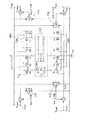
第1の回路例
図3は、本実施形態のインバータ型遅延回路の第1の回路例を示している。図示のように、この遅延回路は、遅延部100aと、遅延部100aの制御電圧VCPとVCNに、電源電圧Vddの変動ΔVddをある割合で加算するためのキャパシタCdp,Csp,Cdn,Csnによって構成されている。
【0054】
キャパシタCdpは、電源電圧Vddと入力端子Tcntpとの間に接続され、キャパシタCspは、入力端子Tcntpと基準電位VSSとの間に接続されている。入力端子Tcntpに、制御電圧Vcntpが入力される。
キャパシタCdnは、電源電圧Vddと入力端子Tcntnとの間に接続され、キャパシタCsnは、入力端子Tcntnと基準電位VSSとの間に接続されている。入力端子Tcntnに、制御電圧Vcntnが入力される。
【0055】
遅延部100aは、直列接続されているn段のインバータINV1,INV2,…,INVnによって構成されている。各インバータは、ゲート及びドレインがそれぞれ共通に接続されているpMOSトランジスタとnMOSトランジスタからなり、pMOSトランジスタのソースと電源電圧Vddとの間にPチャネル側電流源を構成するpMOSトランジスタが接続され、nMOSトランジスタのソースと基準電位VSSとの間にNチャネル側電流源を構成するnMOSトランジスタが接続されている。Pチャネル側電流源を構成するトランジスタのゲートに、制御電圧Vcpが印加され、Nチャネル側電流源を構成するトランジスタのゲートに、制御電圧Vcnが印加される。
【0056】
制御電圧VcpとVcnに応じて、Pチャネル側電流源とNチャネル側電流源の供給電流が制御され、それに応じて、遅延素子として設けられているn段のインバータINV1,INV2,…,INVnの遅延時間が制御される。
【0057】
以下、本例の遅延回路の動作について説明する。
図4は、遅延部100aの構成を示す回路図であり、図5は、当該遅延部100aの動作を示す波形図である。
【0058】
遅延部100aにおいて、遅延段の出力信号立ち下がり時には、Nチャネル側電流源を構成するnMOSトランジスタで律則される駆動電流Ini(i=1,2,…,n)が流れ、遅延段の出力信号立ち上がり時には、Pチャネル側電流源を構成するpMOSトランジスタで律則される駆動電流Ipiが流れる。
【0059】
動作波形において、各遅延段の入力信号レベルが論理しきい電圧VthL を横切った時点から、各遅延段の出力信号レベルが(次段の)論理しきい電圧VthL を横切る時点までを、その遅延段の遅延時間と考え、出力信号立ち下がり時の遅延時間をτni、出力信号立ち上がり時の遅延時間をτpiとおいている。
【0060】
ここで、各遅延段出力の負荷容量をCLiとすると、出力信号立ち下がり時のτniの期間において、負荷容量CLiの電荷はVddからVthL までnMOSの電流源トランジスタにより引き抜かれる。また、出力信号立ち上がり時のτpiの期間において、負荷容量CLiの電荷が0VからVthL までPMOSの電流源トランジスタにより貯められる。
したがって、次式が成立する。
【0061】
【数3】
τni∝CLi×(Vdd−VthL )/Ini …(3)
【数4】
τpi∝CLi×VthL /|Ipi| …(4)
【0062】
ここで、電源電圧の変動Vddがあったとすると、
【数5】
ln(τni) ∝ln(CLi) +ln(Vdd−VthL)−ln(Ini)
Δτni/τni=( ΔVdd−ΔVthL)/( Vdd−VthL)−ΔIni/Ini…(5)
であるから、次の式が得られる。
【0063】
【数6】
Δτni=τni[{( ΔVdd−ΔVthL)/(Vdd−VthL)}−( ΔIni/Ini) ]…(6)
【数7】
Δτpi=τpi{( ΔVthL /VthL)−( Δ|Ipi|/|Ipi|)}…(7)
【0064】
nMOSトランジスタとpMOSトランジスタのバランスをとった設計をした場合、(6)式と(7)式において、Ini=|Ipi|=ID 、τni=τpi=τd、VthL ≒Vdd /2であるから、次式が得られる。
【0065】
【数8】
Δτni≒τd [{( ΔVdd−ΔVthL)/(Vdd/2)}−(ΔIni/ID )]…(8)
【数9】
Δτpi≒τd [{ΔVthL /(Vdd/2)}−(Δ|Ipi|/ID )]…(9)
【0066】
遅延段1段毎に電源ノイズの影響を小さくするためには、Δτni≒0、Δτpi≒0としなければならないから、(8)式と(9)式より、次の式が成り立つことが必要である。
【0067】
【数10】
(ΔVdd−ΔVthL )/(Vdd/2)≒ΔIni/ID …(10)
【数11】
ΔVthL /(Vdd/2)≒Δ|Ipi|/ID …(11)
【0068】
条件を緩和して、連続した遅延段2段毎に電源ノイズの影響を小さくするためには、Δτni+Δτp(i ±1)≒0としなければならないから、(8)式と(9)式より、次式が得られる。
【0069】
【数12】
ΔVdd/(Vdd/2)≒(ΔIni+Δ|Ip(i ±1)|)/ID …(12)
【0070】
制御電圧Vcntnおよび|Vcntp|は、概ね、Vdd/2付近の値であり、nMOSの電流源トランジスタもpMOSの電流源トランジスタも飽和領域で動作する。チャネル長変調効果係数をλn 、λp とすると、チャネル長変調効果も含めた飽和領域の電流式は、次のように与えられる。
【0071】
【数13】
Ini=(1/2) μn Cox(Wni/Lni)(1 +λn VthL)( Vcntn−Vthn)**2 …(13)
【数14】
|Ipi|=(1/2) |μp |Cox(Wpi/Lpi) {1 +|λp |( Vdd−VthL)}(Vcntp−Vthp)**2 …(14)
【0072】
電流源トランジスタのついたインバータ回路の論理しきい電圧については、一般的な定義が存在しないが、インバータ動作するゲート入力信号の電圧が、概ね、Vdd/2のときに遅延段の出力信号の電圧がVthL で釣り合い、Ini=|Ipi|が成り立っていることと定義すると、(13)式、(14)式より、次の式が得られる。
【0073】
【数15】
論理しきい電圧の変動ΔVthL は、(15)式より、次のように求まる。
【数16】
ΔVthL ={|λp |/(λn +|λp |)}ΔVdd…(16)
【0075】
Iniと|Ipi|の変動ΔIni、Δ|Ipi|は、λn と|λp |の値が小さいことを考慮するとチャネル長変調効果も含めた飽和領域の電流式、(13)式、(14)式から求めても、チャネル長変調効果を含めない、次の(17)式、(18)式に示す飽和領域の電流式、から求めても同じような結果を得ることができる。
【0076】
【数17】
Ini=(1/2) μn Cox(Wni/Lni)(Vcntn−Vthn)**2 …(17)
【数18】
|Ipi|=(1/2) |μp |Cox(Wpi/Lpi)(Vcntp−Vthp)**2 …(18)
【0077】
Iniと|Ipi|の変動ΔIni、Δ|Ipi|は、次のように求まる。
【数19】
ΔIni=Ini×2ΔVcntn/(Vcntn−Vthn)…(19)
【数20】
Δ|Ipi|=|Ipi|×2Δ|Vcntp|/|Vcntp−Vthp |…(20)
【0078】
Ini=|Ipi|=ID を考慮して、遅延段1段毎に電源ノイズの影響を小さくするための条件式(10)、(11)に、(16)式、(19)式、(20)式を代入してまとめると、次の式が得られる。
【0079】
【数21】
ΔVcntn≒{λn /(λn +|λp |) }{( Vcntn−Vthn)/Vdd}ΔVdd…(21)
【数22】
Δ|Vcntp|≒{|λp |/(λn +|λp |) }{|Vcntp−Vthp |/Vdd}ΔVdd…(22)
【0080】
即ち、電源電圧の変動があったときに、nNMOSの電流源トランジスタのゲートソース間電圧には、{λn /(λn +|λp |) }{( Vcntn−Vthn)/Vdd}の割合でフィードバックして、pMOSの電流源トランジスタのゲートソース間電圧には、{|λp |/(λn +|λp |) }{|Vcntp−Vthp |/Vdd}の割合でフィードバックすれば遅延時間の変動を非常に小さくできる。
【0081】
また、連続した遅延段2段毎に電源ノイズの影響を小さくするための条件式(12)に、(19)式、(20)式を代入してまとめると、次式が得られる。
【0082】
【数23】
{ΔVcntn/( Vcntn−Vthn)}+{Δ|Vcntp|/|Vcntp−Vthp |) ≒ΔVdd/Vdd…(23)
【0083】
ここで、
【数24】
ΔVcntn≒An ×{( Vcntn−Vthn)/Vdd}ΔVdd…(24)
【数25】
Δ|Vcntp|≒Ap ×{|Vcntp−Vthp |/Vdd}ΔVdd…(25)
とおくと、次式が得られる。
【0084】
【数26】
An +Ap ≒1 …(26)
【0085】
チャネル長変調効果係数はインプラプロファイルに大きく依存するため、λn≠|λp |であることが多いが、仮にλn ≒|λp |として、(21)式、(22)式に代入すると、次式が得られる。
【0086】
【数27】
ΔVcntn≒( 1/2) {( Vcntn−Vthn )/Vdd}ΔVdd…(27)
【0087】
【数28】
Δ|Vcntp|≒( 1/2) {|Vcntp−Vthp |/Vdd}ΔVdd…(28)
少なくとも(24)式、(25)式、(26)式の関係を満足している。
【0088】
図3に示す遅延回路において、電源電圧の変動をバイアス電圧、あるいは、制御電圧に適当な割合で加算するAC的な手段として、nMOSの電流源トランジスタのゲート入力ラインには、接地ラインとの間にキャパシタCsnが設けられ、電源ラインとの間にキャパシタCdnが設けられている。また、pMOSの電流源トランジスタのゲート入力ラインには、電源ラインとの間にキャパシタCdpが設けられ、接地ラインとの間にキャパシタCspが設けられている。
【0089】
AC的な加算手段によれば、接続先の制御電圧ラインが出力がオフの時にハイインピーダンス状態に保持されるチャーチポンプ回路の出力端子やパッシブなループフィルタの出力端子であったとしても、AC的な加算手段はDC的な電流を流さないので、電源ノイズが発生している期間だけ制御電圧に影響を与え、電源ノイズの発生終わった後には副作用となるような余分な制御電圧の変化を引き起こさないという特徴がある。
【0090】
図6と図7は、バイアス回路とAC的加算手段の関係を示す。AC的加算が制御電圧ラインと接地ラインとの間に設けられたキャパシタC1 と、制御電圧ラインと電源ラインとの間に設けられたキャパシタC2 の分圧で行なわれる。電源電圧VddにΔVddの変動があったとすると、図6(a)に示すような等価回路にモデル化される。
【0091】
ΔVbsはバイアス回路出力電圧Vbsの変動で、Rout はバイアス回路の出力抵抗である。この等価回路は、ΔVbs側、即ち、バイアス回路の出力側から見ればロウパスフィルタであり、{C2 /( C1 +C2)}ΔVdd側、即ち、電源電圧Vddの供給側から見ればハイパスフィルタであるので、τAC=Rout ×(C1 +C2 )としたとき、1/τACの周波数を境にして、周波数の高い側で{C2 /(C1 +C2 )}ΔVddの影響が優勢で、周波数の低い側でΔVbs側の影響が優勢となる。
【0092】
ここで、出力バッファ動作時の電源ノイズの幅をtnsとした場合、次の関係
【数29】
τAC=Rout ×(C1 +C2 )>tns…(29)
を満たすように設計すれば、出力バッファ動作時の電源ノイズの影響を低減できる。
【0093】
位相比較回路からアップ信号SUPとダウン信号SDWが出力されていないとき、ハイインピーダンス状態に保持されているチャージポンプの出力端子、または、それに接続するパッシブなループフィルタの出力が制御電圧として入力する場合は、Rout =∞と見なせるので、C1 +C2 の値はループフィルタのキャパシタとして決定すれば良く、C1 とC2 の比は本発明に従い決定すれば良い。
【0094】
図7はAC的加算手段でフィードバックするのと同じように、DC的加算手段においてもフィードバックすることにより、電源ノイズの周波数成分がある程度低くなっても、電源ノイズの影響を低減できる加算手段を示す。AC的加算手段はDC的加算手段のスピードアップコンデンサとして動作するともとれるので、時定数に関係なく一定のフィードバック量を加算することが可能であり、広い周波数成分の電源ノイズに対応することが可能である。
【0095】
図8は、本例の遅延回路を用いた電圧制御発振回路のシミュレーションの結果を示す波形図である。図8において、W1 が電源ノイズがない場合のシミュレーション波形で、W2 が電源ノイズがある場合の従来例のシミュレーション波形で、W3 が電源ノイズがある場合の図3に示す本発明の回路例のシミュレーション波形である。図示のように、本発明の遅延回路において、電源ノイズが発生した場合、電源電圧Vddの変動分に応じて遅延回路を構成する各遅延素子に供給する制御電圧を制御することによって、電源電圧Vddの変動による影響を打ち消すことができ、遅延回路の遅延時間の変動を抑制でき、当該遅延回路を用いて構成される電圧制御遅延回路及び電圧制御発振回路では、ジッタが大幅に低減されることが明らかである。
【0096】
第2の回路例
図9は、本実施形態の遅延回路の第2の回路例を示す回路図である。図示のように、この遅延回路において、遅延部100bはMOSインバータと選択トランジスタ及び電流源トランジスタからなる複数段の遅延素子によって構成されている。
【0097】
MOSインバータは、ゲート及びドレイン同士がそれぞれ接続されているpMOSトランジスタとnMOSトランジスタによって構成されている。ゲート同士の接続点がインバータの入力端子を形成し、ドレイン同士の接続点がそのインバータの出力端子を形成している。図9に示すように、インバータINV1を構成するpMOSトランジスタP1のソースと電源電圧Vddとの間に、電流源トランジスタP11と選択トランジスタP12が直列接続され、また、トラジスタP1のソースと電源電圧Vddとの間に、電流源トランジスタP13が接続されている。インバータINV1を構成するnMOSトランジスタN1のソースと基準電位VSSとの間に、選択トランジスタN12と電流源トランジスタN11が直列接続され、また、トラジスタN1のソースと電源電圧Vddとの間に、電流源トランジスタN13が接続されている。
【0098】
遅延部100bにおいて、各遅延素子におけるPチャネル側の電流源トランジスタのゲートに、制御電圧Vcpが印加され、Nチャネル側の電流源トランジスタのゲートに、制御電圧Vcnが印加される。また、Pチャネル側選択トランジスタのゲートに選択信号/SELHが印加され、Nチャネル側選択トランジスタのゲートに選択信号SELHが印加される。なお、ここで、/SELHは信号SELHの論理反転信号を意味する。なお、他の遅延段を構成する遅延素子については、ほぼ同じ構成を有する。
【0099】
このように構成されている遅延部100bにおいて、選択信号に応じて、各遅延段の遅延素子に供給される電流が制御されるので、インバータに供給する駆動電流が2通りに制御できる。例えば、選択信号SELHがローレベルのとき、各遅延段の遅延素子において、一方の電流源トランジスタのみがインバータに接続される。逆に、選択信号SELHがハイレベルのとき、各遅延段の遅延素子において、両方の電流源トランジスタがともにインバータに接続される。
【0100】
ここで、例えば、各遅延段において、インバータにm個の電流源トランジスタが並列に接続されている。これらの電流源トランジスタのサイズ(チャネル幅/チャネル長)をそれぞれW1/L1 ,W2/L2 ,…,Wm/Lmとすると、インバータに供給される駆動電流ID は、次式によって与えられる。
【0101】
【数30】
また、チャネル長変調係数λ1 、λ2 、…、λm が小さいので、各電流源トランジスタのチャネル長変調係数を等しくλとすると、(30)に基づき次の近似式が得られる。
【0103】
【数31】
ID ≒(1/2) μCox{Σ(Wi/Li) }(1+λVds)(Vcnt −Vth)**2…(31)
【0104】
(13)式、(14)式と(31)式を比較すれば、各遅延素子において電流源トランジスタを並列に接続しても、本発明の電源ノイズの影響の低減方法が有効であることは明らかである。
【0105】
第3の回路例
図10は、本実施形態の遅延回路の第3の回路例を示す回路図である。図示のように、この遅延回路において、遅延部100cはMOSインバータと、インバータの出力端子に接続されているトランスミッションゲートとキャパシタからなる複数の遅延段によって構成されている。即ち、本例の遅延部100cは、いわゆるシャント(分岐)型遅延素子によって構成されている。
【0106】
電源電圧Vddと制御信号入力端子Tcntnとの間にキャパシタCdnが接続されている。キャパシタCdnによって、電源電圧Vddの変動ΔVddが制御電圧Vcntnにフィードバックされる。即ち、本例の遅延回路では、電源電圧Vddの変動に応じて各遅延段に供給される制御電圧Vcntnが制御され、電源電圧の変動による遅延時間の変化を打ち消すように制御が行われるので、電源ノイズの影響を抑制できる。
【0107】
なお、トランスミッションゲートは、例えば、ゲートに制御電圧が印加されるMOSトランジスタによって構成される。図10の例では、各遅延段のインバータの出力端子に接続されているトランスミッションゲートは、ゲートに制御電圧Vcntnが印加されるnMOSトランジスタによって構成される。トランスミッションゲートを構成するトランジスタのソースドレインは、一方がインバータの出力端子に接続され、もう一方はキャパシタを介して基準電位VSSに接続されている。
【0108】
図11は、シャント型遅延素子からなる遅延段の構成を示す回路図である。
図示のように、各遅延段において、インバータの出力端子と基準電位VSSとの間に、分岐用トランスミッションゲートとしてのnMOSトランジスタとキャパシタが直列接続されている。トランジスタのゲートに制御電圧Vcntnが印加される。制御電圧Vcntnに応じて、トランスミッションゲートがオン/オフし、インバータの出力端子の負荷容量が変化するので、遅延時間が制御される。
図12は、入力信号INの立ち上がり時と立ち下がり時のシャント型遅延段の動作を示す波形図である。動作波形は、分岐用のトランスミッションゲート、即ち、キャパシタに直列接続されているトランジスタの制御電圧Vcntnのレベルにより2通りを示してある。
以下、図11及び図12を参照しつつ、本例の遅延回路の動作について説明する。
【0109】
まず、シャント型の遅延段の動作を簡単に説明する。分岐用のトランスミッションゲートは、ソース電圧が基準電位VSSからゲート電圧、即ち、外部から入力される制御電圧Vcntnよりトランジスタのしきい値電圧Vthn 分低いレベルVcntn−Vthn まではオンしているが、ソース電圧がそれ以上の電圧になるとオフしてしまう。したがって、Vcntn−Vthn を境にしてインバータが駆動しなければならない負荷容量が変わり、分岐側の容量をCs 、次段のゲート入力の容量をCg とすると、インバータの出力電圧がVcntn−Vthn 以下のときは、Cg +Csの負荷容量を駆動して、インバータの出力電圧がVcntn−Vthn 以上のときは、Cg の負荷容量を駆動することになる。制御電圧Vcntnのレベルによって重たいCg +Cs の負荷容量を駆動する期間と軽いCg の負荷容量を駆動する期間の割合が変わり、制御電圧Vcntnが高くなると、重たいCg +Cs の負荷容量を駆動する期間の割合が増えるので遅延時間が大きくなる。
【0110】
なお、説明をしやすくするため、制御電圧のトランジスタのしきい電圧1段落ちのレベルを次式によって表す。
【数32】
Vsmax=Vcntn−Vthn (VSB) …(32)
【0111】
ここで、Kを基板効果定数、φ=0.64V、Vthn0はVSB=0Vのときのトランジスタのしきい電圧とすると、次式が得られる。
【数33】
Vthn (VSB)=Vthn0+K{√(VSB+φ)−√φ}…(33)
ただし、VSB=Vsmaxである。
【0112】
Vsmax=Vcntn−Vthn ≦VthL の場合、次の式が成立する。
【数34】
τni∝Cg ×(Vdd−VthL)/Ini…(34)
【数35】
τpi∝( Cg ×VthL +Cs ×Vsmax)/|Ipi|…(35)
【0113】
(34)式と(35)式によって、さらに次の式が得られる。
【0114】
【数36】
Δτni≒τni× [{( ΔVdd−ΔVthL)/(Vdd−VthL)}-(ΔIni/Ini)]…(36)
【数37】
Δτpi≒τpi×[{( Cg ×ΔVthL +Cs ×ΔVsmax) /(Cg ×VthL +Cs ×Vsmax) }−(Δ|Ipi|/|Ipi|) ]…(37)
【0115】
また、Vsmax=Vcntn−Vthn ≧VthL の場合、次の式が成立する。
【数38】
τni∝{Cg ×(Vdd−VthL)+Cs ×(Vsmax−VthL)}/Ini …(38)
【数39】
τpi∝( Cg +Cs)×VthL /|Ipi|…(39)
【0116】
(38)式と(39)式によって、さらに次の式が得られる。
【数40】
Δτni≒τni×([{Cg ×( ΔVdd−ΔVthL)+Cs ×(ΔVsmax−ΔVthL)}/{Cg ×(Vdd−VthL)+Cs ×(Vsmax−VthL)}]−(ΔIni/Ini) )…(40)
【数41】
Δτpi≒τpi×{( ΔVthL /VthL)−(Δ|Ipi|/|Ipi|) }…(41)
【0117】
ここで、インバータの論理しきい電圧VthL は、次のように与えられる。
【数42】
VthL =[Vdd−|Vthp |+Vthn ×√{(μnWni/Lni)/(μpWpi/Lpi)}]/[1+√{(μnWni/Lni)/(μpWpi/Lpi)}]…(42)
【0118】
(42)式により、次式が得られる。
【数43】
ΔVthL =ΔVdd/[1+√{(μnWni/Lni )/(μpWpi/Lpi)}]…(43)
【0119】
制御電圧Vcntnのとりうる最大の電圧が電源電圧Vddとすると、Vsmax=Vcntn−Vthn であるから、Vsmax のとりうる最大の電圧は、概ね、0.7×Vddとなる。
このため、シャント型遅延回路を設計する場合、インバータの論理しきい値電圧VthL をVdd/2よりも低めに設計する。ここで、仮に、次の式が成り立つとする。
【数44】
{(μnWni/Lni)/(μpWpi/Lpi)}=2…(44)
【0120】
また、Vthn ≒Vdd/6程度と考えると、(42)式と(43)式は、それぞれ次の式に近似できる。
【数45】
VthL ≒0.44×Vdd …(45)
【数46】
ΔVthL ≒0.41×ΔVdd …(46)
【0121】
インバータの出力電圧がVthL 付近まで変化したときには、Ini、Ipiは非飽和となるが、遅延時間の定義した期間においては、概ね、飽和領域で動作しているので、次の式が成立する。
【数47】
Ini∝(1/2) μn Cox(Wni/Lni)( Vdd−Vthn)**2 …(47)
【数48】
|Ipi|∝(1/2) |μp |Cox(Wpi/Lpi)( Vdd−|Vthp |)**2…(48)
【0122】
(47)式と(48)式より、
【数49】
ΔIni≒Ini×{2ΔVdd/(Vdd−Vthn)}…(49)
【数50】
Δ|Ipi|≒|Ipi|×{2ΔVdd/(Vdd−|Vthp |) }…(50)
【0123】
また、(44)式の仮定により、次式が得られる。
【数51】
また、(32)式、(33)式より、次式が得られる。
【数52】
ΔVsmax=ΔVcntn/[1+K/{2√(Vsmax+φ)}]…(52)
【0125】
基板効果定数Kは0.5前後の値であり、Vsmaxは0.44×Vdd付近の値であることを考慮すると、(52)式は、次のように近似される。
【数53】
Vsmax≒0.85×ΔVcntn…(53)
【0126】
シャント型の遅延段の場合は負荷容量値が途中で変わるため、これ以上、一般的に考えるのは困難なため、Cs =10×Cg という条件で、Vsmax=0.34×Vddの場合と、Vsmax=0.54×Vddの場合について考える。また、Vthn≒|Vthp |≒Vdd/6とする。
【0127】
Vsmax=0.34×Vdd≦VthL =0.44×Vddの場合、(34)式から(37)式に、(45)式、(46)式、(49)式、(50)式、(51)式、及び(53)式を代入することにより、次の式が得られる。
【0128】
【数54】
τni∝0.28×Cg ×Vdd/ID …(54)
【数55】
τpi∝3.84×Cg ×Vdd/ID …(55)
【0129】
【数56】
Δτni≒τni×{(−1.35×ΔVdd)/Vdd}…(56)
【数57】
Δτpi≒τpi×[{(−2.29×ΔVdd+(2.21×ΔVcntn) }/Vdd]…(57)
【0130】
(54)式から(57)式により、次式が得られる。
【数58】
Δτni+Δτp(i ±1)∝{( −9.17×ΔVdd) +(8.49×ΔVcntn)}×Cg /ID …(58)
【0131】
ここで、Δτni+Δτp(i ±1)≒0とするためには、次式を満たせばよい。
【数59】
Vcntn≒1.08× Vdd …(59)
ΔVcntn≒ΔVddとして、制御電圧Vcntnを電源電圧Vddの変動に合わせて揺らした場合、電源ノイズの影響を(9.17−8.49)/9.17≒7%に低減することが見込まれる。
【0132】
Vsmax=0.54×Vdd≧VthL =0.44×Vddの場合、(38)式から(41)式に、(45)式、(46)式、(49)式、(50)式、(51)式、及び(53)式を代入することにより、次式が得られる。
【0133】
【数60】
τni∝0.78×Cg ×Vdd/ID …(60)
【数61】
τpi∝4.84×Cg ×Vdd/ID …(61)
【0134】
【数62】
Δτni≒τni×[{(−4.65×ΔVdd) +(5.45×ΔVcntn) }/Vdd]…(62)
【数63】
Δτpi≒τpi×{(−1.47×ΔVdd)/Vdd}…(63)
【0135】
(60)式から(63)式により、さらに次式が得られる。
【数64】
Δτni+Δτp(i ±1 )∝{(−10.74×ΔVdd) +(4.25×ΔVcntn) }×Cg /ID …(64)
【0136】
Δτni+Δτp(i ±1 )≒0とするためには、次式を満たせばよい。
【数65】
ΔVcntn≒2.53×ΔVdd…(65)
ΔVcntn≒ΔVddとして、制御電圧Vcntnを電源電圧Vddの変動に合わせて揺らした場合、電源ノイズの影響を(10.74−4.25)/10.74≒60%に低減することが見込まれる。
【0137】
以上をまとめると、シャント型の遅延段において、分岐用のトランスミッションゲートがNMOSトランジスタの場合には、制御電圧ラインと電源ラインとの間にキャパシタを設けることにより、また、分岐用のトランスミッションゲートがPMOSトランジスタの場合には、制御電圧ラインと接地ラインとの間にキャパシタを設けることにより、電源ノイズの影響を概ね半減することができる。
【0138】
第2実施形態
図13は本発明に係る遅延回路の第2の実施形態を示す概念図である。
本実施形態の遅延回路では、それぞれ異なる電源電圧依存性を有する電流源の供給電流を加算して駆動電流を生成することによって、電源ノイズによる遅延時間の変動を抑制し、電源ノイズの影響を低減する。
【0139】
図示のように、本実施形態の遅延回路は、直列接続されている複数の遅延段によって構成されている。各遅延段は、例えば、スイッチングトランジスタまたはセレクタトランジスタを含む遅延素子と、遅延素子に駆動電流を供給する電流源によって構成されている。例えば、図示のように、遅延素子と電源電圧Vddとの間に、少なくとも2ヶ以上の駆動電流Id1,Id2,…,Idjを供給する電流源が並列に接続され、遅延素子と基準電位VSSとの間に、少なくとも2ヶ以上の駆動電流Is1,Is2,…,Isjを供給する電流源が並列に接続されている。
【0140】
さらに、それぞれの電流源には異なる電源電圧依存性を有する。即ち、電源電圧VddがΔVdd分変化した場合、各電流源にそれぞれΔId1,ΔId2,…,ΔIdj及びΔIs1,ΔIs2,…,ΔIsjの変化が生じたとすると、ΔId1/Id1≠ΔId2/ΔId2,…,≠ΔIdj/Idj、同じく、ΔIs1/Is1≠ΔIs2/ΔIs2,…,≠ΔIsj/Isj。
【0141】
電源ライン側の同時にオンしている電流源の電流の和が出力立ち上がり時の駆動電流となり、即ち、Id =ΣIdjである。その変化量は、ΔId =ΣΔIdjとなる。
一方、接地ライン側の同時にオンしている電流源の電流の和が出力立ち下がり時の駆動電流となり、即ち、Is =ΣIsj、その変化量は、ΔIs =ΣΔIsjとなる。
【0142】
ここで、τofi を遅延段出力立ち下がり時の遅延時間、τori を遅延段出力立ち上がり時の遅延時間とすると、電源電圧VddにΔVddの変動があったときに、前記の(6)式、(7)式と同じような関係式が書ける。
【0143】
【数66】
Δτofi =τofi [{( ΔVdd−ΔVthL)/( Vdd−VthL)}−( ΣΔIsj/ΣIsj) ]…(66)
【数67】
Δτori =τori {( ΔVthL /VthL)−( ΣΔIdj/ΣIdj) ]…(67)
【0144】
Δτofi ≒0及びΔτori ≒0とするためには、出力振幅の相対的な変化量(ほぼ電源電圧の相対的な変化量ΔVddに等しい)と電流源の電流値の和の相対的な変化量(駆動電流の相対的な変化量に等しい)が一致するように設計すれば良い。即ち、次の式が得られる。
【0145】
【数68】
{( ΔVdd−ΔVthL)/( Vdd−VthL)}=( ΣΔIsj/ΣIsj) …(68)
【数69】
( ΔVthL /VthL)=( ΣΔIdj/ΣIdj)…(69)
【0146】
ΣIsj≒ΣIdj≒ID , VthL ≒Vdd/2 の場合、(12)式と同様に、
ΔVdd/(Vdd/2)≒(ΣΔIsj+ΣΔIdj)/ID
【0147】
図14は、本実施形態の遅延回路の一例を示す構成図である。
図示のように、本実施形態の遅延回路は、遅延部200、交流加算回路(AC加算回路)110,112,114,116によって構成されている。
図示されていない位相比較器やチャージポンプ回路やループフィルタやバイアス回路などにより、バイアス電圧Vcntn1,Vcntp1,Vcntn2,Vcntp2が供給される。
【0148】
遅延部200は、例えば、直列接続されている複数の遅延素子によって構成されている。なお、本実施形態の遅延部200を構成する遅延素子は、例えば、CMOSインバータを含み、入力信号に対して所定の遅延時間を与えた論理反転信号を出力する。各遅延素子の遅延時間の合計が遅延部200の遅延時間TD である。
【0149】
AC加算回路110,112,114と116は、それぞれ電源電圧Vddと基準電位VSSとの交流成分に所定の係数を掛けた結果をそれぞれΔVcn1,ΔVcp1,ΔVcn2,ΔVcp2として出力し、バイアス電圧(または制御電圧)とAC加算回路の出力とを加算し、加算結果が制御電圧として遅延部100に供給される。
【0150】
遅延部200において、各遅延段はMOS型インバータと電流源トランジスタによって構成されている。例えば、図示のように、1段目の遅延段は、pMOSトランジスタP1とnMOSトランジスタN1で構成されているインバータINV1、インバータINV1のPチャネル側に電流を供給する電流源トランジスタP11,P12、インバータINV1のNチャネル側に電流を供給する電流源トランジスタN11,N12によって構成されている。
【0151】
Pチャネル側電流源トランジスタP11のゲートに制御電圧Vcp1 が印加され、トランジスタP12のゲートに制御電圧Vcp2 が印加される。
Nチャネル側電流源トランジスタN11のゲートに、制御電圧Vcn1 が印加され、トランジスタN12のゲートに制御電圧Vcn2 が印加される。
【0152】
上述した構成を有する遅延部200において、各遅延段の遅延時間は、それぞれの遅延段のインバータに供給される電流によって制御される。本発明では、それぞれの遅延段に供給される電流が異なる電源電圧依存性を持つように制御されていることで、電源ノイズの影響を抑制できる。
【0153】
(19)式、(20)式の関係より、(68)式、(69)式は、図14に対応した形に、それぞれ次のように書き換えられる。
【0154】
【数70】
{( ΔVdd−ΔVthL)/( Vdd−VthL)}
=(Σ[{2×Isj/(Vcntnj −Vthn)}ΔVcnj ]/ΣIsj)…(70)
【数71】
( ΔVthL /VthL)
=(Σ[{2×Ipj×|Vcntpj −Vthp |}Δ|Vcpj |]/ΣIdj)…(71)
【0155】
さらに、図14において、ΔVcnj =kcnj ΔVdd、Δ|Vcpj |=kcpj ΔVddであり、仮に、VthL ≒Vdd/2、Vcntnj ≒|Vcntpj |≒Vdd/2、Vthn ≒|Vthp |≒Vdd/6とすると、(70)式と(71)式との関係は、次に示すように、kcnj とIsj、kcpj とIdjのみで書き表すことができる。
【0156】
【数72】
6×Σ(kcnj ×Isj) ≒ΣIsj …(72)
【数73】
6×Σ(kcpj ×Idj) ≒ΣIdj …(73)
【0157】
(72)式と(73)式及び上記の仮定を満足する場合、電源ノイズの影響を非常に小さくすることが可能である。
【0158】
例えば、今、kcn1 =0、kcn2 =0.5としたとき、(72)式は、
6×{0×Is1+0.5×Is2}≒{Is1+Is2}となり、
(Is1/Is2)≒(2/1)で設計すれば良い。
【0159】
また、kcn1 =0、Kcn2 =1.0としたとき、(72)式は、
6×{0×Is1+1.0×Is2}≒{Is1+Is2}となり、
(Is1/Is2)≒(5/1)で設計すれば良い。
【0160】
また、kcn1 =0.05、Kcn2 =0.5としたとき、(72)式は、
6×{0.05×Is1+0.5×Is2}≒{Is1+Is2}となり、
(Is1/Is2)≒(2.86/1)で設計すれば良い。
【0161】
第1の回路例
図15は本発明に係る遅延回路の第2の実施形態を適用した第1の回路例を示す回路図である。
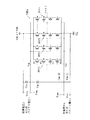
図示のように、本例の遅延回路は、遅延部200a及び当該遅延部200aに制御電圧あるいはバイアス電圧を供給するAC加算手段によって構成されている。遅延部200aは、電源ライン側および接地ライン側にMOS型の電流源トランジスタが設けられているインバータ型の遅延段によって構成され、電流源の制御電圧あるいはバイアス電圧として、Vcntp1 、Vcntp2 、Vcntn1 、Vcntn2が供給されている。
【0162】
例えば、初段の遅延段において電源ライン側の電流源は、Vcntp1 がゲートソース間に入力され、トランジスタサイズがWp1/Lp1のPMOS電流源トランジスタP11と、Vcntp2 がゲートソース間に入力され、トランジスタタイズがWp2/Lp2のPMOS電流源トランジスタP12が並列に接続している。
また、初段の遅延段の接地ライン側の電流源は、Vcntn1 がゲートソース間に入力され、トランジスタサイズがWn1/Ln1のNMOS電流源トランジスタN11と、Vcntn2 がゲートソース間に入力され、トランジスタサイズがWn2/Ln2のNMOS電流源トランジスタN12が並列に接続している。
【0163】
制御電圧またはバイアス電圧Vcntp1 、Vcntp2 、Vcntn1 、Vcntn2 の供給ラインには、電源電圧の変動をある適当な割合でフィードバックするAC的加算手段が設けられている。
例えば、初段の遅延段において、上記のトランジスタN11のVgsにおけるΔVcn1 の電圧を加算するAC的な手段は、NMOS1のゲート入力ラインと接地ラインの間に設けられたキャパシタCsn1 とN11のゲート入力ラインと電源ラインの間に設けられたキャパシタCdn1 によるAC的な分圧回路で構成され、トランジスタN12のVgsにおけるΔVcn2 の電圧を加算するAC的な手段は、N12のゲート入力ラインと接地ラインとの間に設けられたキャパシタCsn2 とN12のゲート入力ラインと電源ラインとの間に設けられたキャパシタCdn2 によるAC的な分圧回路で構成される。
【0164】
トランジスタP11のVgsにおけるΔVcp1 の電圧を加算するAC的手段は、P11のゲート入力ラインと電源ラインとの間に設けられたキャパシタCdp1 とP11のゲート入力ラインと接地ラインの間に設けたキャパシタCsp1 によるAC的分圧回路で構成され、トランジスタP12のVgsにおけるΔVcp2の電圧を印加するAC的手段は、P12のゲート入力ラインと電源ラインの間に設けたキャパシタCdp2 とP12のゲート入力ラインと接地ラインの間に設けたキャパシタCsp2 によるAC的な分圧回路で構成される。
【0165】
即ち、分圧回路によって得られた制御電圧の変動分は、それぞれ次式によって求められる。
【数74】
【数75】
(19)式と(20)式の関係より、(70)式、(71)式は、図15に対応した形に、それぞれ次のように書き換えられる。
【数76】
【数77】
上記の(74)式から(77)式を満足するように遅延回路を設計することにより、電源ノイズの影響の小さいインバータ型の遅延回路、電圧制御遅延回路、電圧制御発振回路を実現できる。
【0170】
(3)式から(28)式の導出過程を参考にすると、ΔVthL が分からない場合でも、VthL ≒Vdd/2で、連続した遅延段2段で電源ノイズの影響を吸収できれば良い場合には、(76)式と(77)式の左辺は、ΔVdd/Vddに置き直すことが可能である。即ち、次の式が得られる。
【0171】
【数78】
第2の回路例
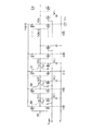
図16は本発明に係る遅延回路の第2の実施形態を適用した第2の回路例を示す回路図である。
図示のように、本例の遅延回路は、図15に示す本実施形態の第1の回路例と異なる点は、本例の遅延回路において制御電圧あるいはバイアス電圧として供給されるVcntp1 、Vcntp2 、Vcntn1 、Vcntn2 のうち、Vcntp2 とVcntn2 については、AC的加算手段が設けられているが、Vcntp1 とVcntn1 については、キャパシタの分圧によるAC的加算手段が設けられているのではなく、電源電圧の変動の影響を防ぎ、ゲートソース間電圧を安定化させるためのキャパシタCdp1 ,Csn1 のみ設けられている点である。
【0173】
トランジスタNM11のVgsにおける電源電圧の変動ΔVddによる影響を発生しにくくする手段として、N11のゲート入力ラインと接地ラインとの間にキャパシタCsn1 が設けられており、トランジスタP11のVgsにおける電源電圧の変動による影響を発生しにくくする手段として、P11のゲート入力ラインと電源ラインとの間にキャパシタCdp1 が設けられている。即ち、ΔVcn1=0、ΔVcp1=0である。このため、入力される制御電圧またはバイアス電圧Vcntp1 とVcntn1 は、電源電圧Vddの変動による影響を受けることなく、遅延部200aに供給される。
【0174】
遅延部200aにおいて、例えば、初段の遅延段では、CMOSインバータの電源ライン側に接続されている電流源トランジスタP11のゲートに、制御電圧Vcp1 =Vcntp1 が印加され、電流源トランジスタP12のゲートに、制御電圧Vcp2 =Vcntp2 +ΔVcp2 が印加される。
一方、CMOSインバータの接地ライン側に接続されている電流源トランジスタN11のゲートに、制御電圧Vcn1 =Vcntp1 が印加され、電流源トランジスタN12のゲートに、制御電圧Vcn2 =Vcntp2 +ΔVcn2 が印加される。
【0175】
トランジスタN12のVgsへのAC的な加算手段は、N12のゲート入力ラインと接地ラインとの間に設けられたキャパシタCsn2とN12のゲート入力ラインと電源ラインとの間に設けられたキャパシタCdn2からなるAC的な分圧回路で構成され、トランジスタP12のVgsへのAC的な加算手段は、P12のゲート入力ラインと電源ラインとの間に設けられたキャパシタCdp2とP12のゲート入力ラインと接地ラインとの間に設けられたキャパシタCsp2からなるAC的な分圧回路で構成されている。即ち、電源電圧Vddの変動ΔVddによって制御電圧Vcntn2 とVcntp2 に与える影響ΔVcn2 とΔVcp2 は、それぞれ次式によって求まる。
【0176】
【数80】
ΔVcn2 ={Cdn2 /(Csn2 +Cdn2 )}×ΔVdd…(80)
【数81】
|ΔVcp2 |={Csp2 /(Cdp2 +Csp2 )}×ΔVdd…(81)
キャパシタCsn2 ,Cdn2 及びCdp2 ,Csp2 の値は、AC的分圧とDC的な分圧が一致するような比に設定する。即ち、次式が得られる。
【0177】
【数82】
{Cdn2 /(Csn2 +Cdn2 )}=(Vcntn2 /Vdd)…(82)
【数83】
{Csp2 /(Cdp2 +Csp2 )}=(|Vcntp2 |/Vdd)…(83)
【0178】
したがって、ΔVcn2 とΔVcp2 は、それぞれ次式によって求まる。
【数84】
ΔVcn2 =(Vcntn2 /Vdd)×ΔVdd…(84)
【数85】
ΔVcp2 =(Vcntp2 /Vdd)×ΔVdd…(85)
【0179】
ここで、ΔVcn=0、ΔVcp1=0および(84)式、(85)式を(78)式と(79)式へ代入してまとめると、電源ノイズの影響を小さくできるトランジスタサイズの比は、次式によって与えられる。
【0180】
【数86】
{(Wn1/Ln1)/(Wn2/Ln2)}
≒{(Vcntn2 −Vthn )(Vcntn2 +Vthn)}/{(Vcntn1-Vthn)**2 }…(86)
【数87】
{(Wp1/Lp1)/(Wp2/Lp2)}
≒{(Vcntp2 −Vthp)( Vcntp2 +Vthp)}/{(Vcntp1-Vthp)**2 }…(87)
【0181】
例えば、Vcntn1 ≒|Vcntp1 |≒(1/2)Vdd、Vcntn2 ≒|Vcntp2 |≒(√5/6)Vdd≒0.373 Vdd、さらにVthn ≒|Vthp |≒(1/6) Vddの場合に、{(Wn1/Ln1)/(Wn2/Ln2)}≒{(Wp1/Lp1) /(Wp2 /Lp2) }≒1となる。
【0182】
このような回路構成にすることで、好適には、Vcntn1とVcntp1の方を、チャージポンプ出力に連なる制御電圧専用の供給ラインとして用いて、Vcntp2 とVcntn2 の方を、電源ノイズの影響を低減するためのバイアス電源専用の供給ラインとして用いるというように目的を分けて設計することができる。
さらに好適には、Vcntn2 を発生するバイアス回路およびVcntp2 を発生するバイアス回路130と132を設けて、それらのバイアス回路は電源ノイズの影響を低減するためのDC的な加算手段としての働きをさせる。
【0183】
バイアス電圧Vcntn2 を発生するバイアス回路132において、電流源トランジスタN12のゲート入力ラインと接地ラインとの間に、抵抗成分Rsn2と電流源トランジスタN12のゲート入力ラインと電源ラインとの間の抵抗成分Rdn2の分圧比により、次式に示す分圧電圧Vcntn2 が発生される。
【0184】
【数88】
Vcntn2 ={Rsn2 /(Rsn2 +Rdn2 )}×Vdd…(88)
【0185】
バイアス電圧Vcntp2 を発生するバイアス回路130において、電流源トランジスタP12のゲート入力ラインと電源ラインとの間の抵抗成分Rdp2と電流源トランジスタP12のゲート入力ラインと接地ラインとの間の抵抗成分Rsp2の分圧比により、次式に示す分圧電圧Vcntp2 が発生される。
【0186】
【数89】
|Vcntp2 |={Rdp2 /(Rdp2 +Rsp2 )}×Vdd…(89)
【0187】
DC的な加算は、当然なことながら、(88)式、(89)式より、それぞれ次式のように求められる。
【0188】
【数90】
ΔVcn2 =(Vcntn2 /Vdd)×ΔVdd…(90)
【数91】
ΔVcp2 =(Vcntp2 /Vdd)×ΔVdd…(91)
【0189】
本例の遅延回路において、キャパシタからなるAC的な加算手段だけでなく、抵抗素子で構成されるDC的な加算手段も備わっているため、広い周波数成分の電源ノイズに対して有効である。
【0190】
第3の回路例
図17は本発明に係る遅延回路の第2の実施形態を適用した第3の回路例を示す回路図である。本回路例が図16に示す第2の回路例と異なる点は、制御電圧あるいはバイアス電圧として供給されるVcntp1 、Vcntp2 、Vcntn1 、Vcntn2 のうち、Vcntp2 とVcntn2 が共通のラインで供給される点である。
【0191】
図17に示すように、遅延部200aにおいて、各遅延段の電源ライン側の電流源トランジスタに供給される制御電圧Vcp2 =Vcntp2 +ΔVcp2 と接地ライン側の電流源トランジスタに供給される制御電圧Vcn2 =Vcntn2 +ΔVcn2 は、同じ制御電圧ラインで供給される。
【0192】
例えば、初段の遅延段において、接地ライン側の電流源トランジスタN12のゲート入力ラインと電源ライン側の電流源トランジスタP12のゲート入力ラインは共通であり、概ね、トランジスタN12とトランジスタP12の実効的なゲートソース間電圧が同じになるような制御電圧(Vcp2 とVcn2 )が基準電圧発生回路140により供給される。
【0193】
即ち、次の式が成り立つ。
【数92】
Vcntn2 −Vthn ≒|Vcntp2 −Vthp |…(92)
【0194】
ところで、Vcntn2 +|Vcntp2 |=Vddであるから、次の式が得られる。
【数93】
Vcntn2 ≒(Vdd+Vthn −|Vthp |)/2≒Vdd/2…(93)
【数94】
|Vcntp2 |≒(Vdd+|Vthp |−Vthn )/2≒Vdd/2…(94)
【0195】
図17に示すように、DC的加算手段を兼ねた基準電圧発生回路は、好適には、電流源トランジスタN12とP12の共通のゲート入力ラインと接地ラインとの間の抵抗成分Rs2と、電流源トランジスタN12とP12の共通のゲート入力ラインと電源ラインとの間の抵抗成分Rd2で構成されている分圧回路142を含む。
【0196】
即ち、バイアス電圧は、DC的な分圧により生成される。
【数95】
Vcntn2 ={Rs2/(Rs2+Rd2)}×Vdd≒Vdd/2…(95)
【数96】
|Vcntp2 |={Rd2/(Rs2+Rd2}×Vdd≒Vdd/2…(96)
なお、ここで、Rs2≒Rd2である。
抵抗部分Rs2,Rd2はMOSトランジスタなどで形成しても良い。
【0197】
また、図18に示すように、DC的加算手段を兼ねた基準電圧発生回路は、好適には、電源ライン側に設けられたVthp 分の電圧を発生するためのゲートとドレインが接続したPMOSトランジスタと、接地ライン側に設けられたVthn 分の電圧を発生するためのゲートとドレインが接続したNMOSトランジスタと、上記、2つのトランジスタのドレイン間を直列に接続する同じ抵抗値の2つの抵抗素子Rd2とRs2からなる分圧回路142aを含む。分圧回路142aにおいて、2つの抵抗素子d2とRs2の接続中点より基準電圧(バイアス電圧)が出力される。
なお、図18において、分圧回路142aを除けば、他の各構成部分は、図17に示す第3の回路例とほぼ同じである。
【0198】
遅延部200aにおいて、例えば、初段の遅延段の電流源トランジスタN12のVgsへのAC的な加算手段及び電流源トランジスタP12のVgsへのAC的な加算手段は、共通のゲート入力ラインと接地ラインのと間に設けられたキャパシタCs2と共通のゲート入力ラインと電源ラインとの間に設けられたキャパシタCd2によるAC的な分圧による。なお、図17及び図18において、Cs2 ≒Cd2 である。
即ち、遅延部200aの電源ライン側電流源トランジスタに供給される制御電圧Vcp2及び接地ライン側トランジスタに供給される制御電圧Vcn2は、それぞれ次式によって求まる。
【0199】
【数97】
ΔVcn2 ={Cd2/(Cs2+Cd2)}×ΔVdd≒ΔVdd/2…(97)
【数98】
|ΔVcp2 |={Cs2/(Cd2+Cs2)}×ΔVdd≒ΔVdd/2…(98)
【0200】
さて、バイアス電圧側、即ち、電圧Vcntn2 とVcntp2 側において、Vcntn2≒|Vcntp2 |≒Vdd/2であり、制御電圧側、即ち、電圧Vcntn1 とVcntp1側においても、Vcntn1 ≒|Vcntp1 |≒Vdd/2であるとすると、(86)式と(87)式より、電源ノイズの影響を小さくできるトランジスタサイズの比は、次式によって与えられる。
【0201】
【数99】
{(Wn1/Ln1)/(Wn2/Ln2)}=[{( Vdd/2)+Vthn)/{( Vdd/2)−Vthn }]…(99)
【数100】
{(Wp1/Lp1)/(Wp2/Lp2)}=[{( Vdd/2)+|Vthp |)}/{( Vdd/2)−|Vthp |}]…(100)
【0202】
例えば、Vthn ≒|Vthp |≒(1/6) Vddの場合、{(Wn1/Ln1)/(Wn2 /Ln2)}≒{(Wp1/Lp1)/(Wp2 /Lp2)}≒2となる。
【0203】
このような回路構成にすると、AC的加算手段に必要なキャパシタの個数とDC的加算手段に必要な抵抗素子の個数が半分にできるし、好適には、制御電圧の反転電圧を発生させるための基準電圧(≒Vdd/2)発生回路の出力をそのまま利用することにより、回路規模の増加を遅延段の電流源トランジスタの増加のみに抑えられるという利点がある。
【0204】
図20は、図17及び図18に示す本発明の第2の実施形態を適用した第3の回路例を電圧制御発振回路に適用した場合のシミュレーションの結果を示している。図20において、W4 が電源ノイズがない場合のシミュレーション波形で、W5 が電源ノイズがある場合の従来例を用いたシミュレーション波形で、W6 が電源ノイズがある場合の本第3の回路例を用いたシミュレーション波形である。図示のように、本発明の第2の実施形態を適用した遅延回路により、電源ノイズによる影響が大幅に低減され、ジッタが大幅に低減できることが明らかである。
【0205】
図19に本発明の第2の実施形態の第3の回路例のさらに別の構成例を示す。
図18に示した構成例と異なる点は、遅延段を構成するインバータが差動構成になっている点である。このように差動構成の遅延段にはなっているが、遅延時間の制御電圧依存性は、カレントミラー型のような本当の差動型の遅延段の特性よりも、インバータ型の遅延段の特性に近いため、本発明の電源ノイズの影響を低減する方法を適用できる。
【0206】
第3の実施形態
本実施形態では、上述した本発明の第1及び第2実施形態における電源ノイズの影響の低減方法を適用した電圧制御遅延回路、あるいは、電圧制御発振器の制御電圧範囲、発振周波数範囲を拡大する方法にを明らかにする。
【0207】
まず、ここで、τofi を遅延段出力立ち下がり時の遅延時間、τori を遅延段出力立ち上がり時の遅延時間とすると、電流源型の遅延段について、本発明の第1あるいは第2の実施形態における電源ノイズの影響の低減方法をまとめた式は以下のように書き表せる。
【0208】
【数101】
【数102】
Δτori =τori {( ΔVthL /VthL)−[2Σ{(Wpj/Lpj)(|Vcntpj −Vthp |) kcpj ΔVdd}/Σ{(Wpj/Lpj) (Vcntpj −Vthp)**2 }])…(102)
【0210】
さて、Vdd−VthL ≒VthL≒Vdd/2で、Vcntnj =|Vcntpj |=Vctypとすると、(101)式と(102)式は、下記に変形される。
【0211】
【数103】
Δτofi =τofi ×( ΔVdd/Vdd) ×{1−( {Vdd/(Vctyp−Vthn)}{2Σ{(Wnj/Lnj) kcnj }/Σ(Wnj/Lnj) ])…(103)
【0212】
【数104】
Δτori =τori ×( ΔVdd/Vdd) ×{1−({Vdd/(Vctyp−|Vthp|) }[2Σ{(Wpj/Lpj) kcpj }/Σ(Wpj/Lpj) ]…(104)
【0213】
(103)式と(104)式において、{Vdd/(Vctyp−Vthn)}及び{Vdd/(Vctyp−|Vthp |) }の項は、電源電圧Vddや制御電圧Vctypに関係なく、一定の値に保てば、特定のkcnj 、kcpj 、Wnj/ Lnj、Wpj/ Lpjの組み合わせでも、制御電圧Vctypに関係なくΔτofi ≒Δτori ≒0とすることができる。即ち、次式を満足するようなフィードバックループを設ければ良い。
【0214】
【数105】
k1 ×Vdd≒Vctyp−Vthn …(105)
【0215】
ただし、Vctypに追従してVddも変化するため、Vctypに対する遅延時間の変化率(即ち、VCO回路のゲイン)が約2/3に落ちて発振周波数域が狭くなることと、Vctypの電圧に従って、遅延段出力の振幅が変化するため、他の回路とのインターフェイスを考えなければいけないことに注意する必要がある。さらに、外付け回路で遅延段のVddを発生させる場合には、Vctypの最大電圧に対応したVddの最大電圧がデバイスの最大電圧を越える恐れがあることなどに、注意を要する。
【0216】
図21は、本発明の第3の実施形態の遅延回路、電圧制御遅延回路及び電圧制御発振回路を示す構成図である。
図示のように、本実施形態では、電源ノイズの影響を低減できる制御電圧範囲、発振周波数範囲を拡大するため、制御電圧と電源電圧が一定の関係を保つ手段が設けられる。
【0217】
図21では、PLL、またはDLLにより制御電圧Vcntn1 を制御して、Vcntn1 により遅延回路(または電圧制御遅延回路、電圧制御発振回路)に供給される電源電圧Vddを制御する場合の回路例である。
なお、図22は、PLL、DLLにより遅延回路に供給される電源電圧Vddを制御し、さらに電源電圧VddによりVcntn1 を制御する場合の回路例である。さらに、図23は(105)式の関係を成り立たせるための参照電圧Vcmp を発生するための参照電圧発生回路170を示す回路図である。
【0218】
図23において、参照電圧Vcmp は、次式によって与えられる。
【数106】
Vcmp ={R1 /(R1 +R2 )}×(Vdd−VGS)+VGS…(106)
【0219】
さらに、図21及び図22に示す回路において、Vctyp=Vcmp になるように制御されるので、(102)式、(103)式より、次式が得られる。
【数107】
(R2 /R1 )={(1−k1 )/k1 }…(107)
【数108】
VGS={1/(1−k1 )}×Vthn …(108)
【0220】
(108)式より、図23における電圧VGSを発生するトランジスタは、k1の値によっては、2段あるいは3段でも良い。また、VGSを発生するトランジスタがなく抵抗だけの分圧による場合でもある程度の効果は得られる。
【0221】
(103)式、(104)式における{Vdd/(Vctyp−Vthn)}及び{Vdd/(Vctyp−|Vthp |) }の値を一定に保つその他の方法として、これらの項とkcnj やkcpj を掛け合わせた値の変動を少なくする方法が考えられる。kcnj とkcpj は、(74)式、(75)式で与えられるが、これらのキャパシタを接合容量で形成したとする。
【0222】
第4の実施形態
図24は、本発明の遅延回路、電圧制御遅延回路または電圧制御発振回路の第4の実施形態を示す回路図である。本実施形態では、電源ノイズの影響を低減できる制御電圧範囲、発振周波数範囲を拡大するため、AC的加算手段を構成する容量素子に電圧可変容量素子、即ち接合容量素子を用いる。
【0223】
通常、半導体素子に生成される接合容量Cjの容量値は、次式によって与えられる。
【数109】
Cj (VBD) ≒C0 /{(Vpb+VBD)**mj }…(109)
【0224】
(109)式において、VBDは外部からPN接合に印加される逆バイアス電圧、Cj(VBD)は、電圧VBDが印加されるときの容量値、Vpb及びmjは、デバイス定数である。
通常シリコン(Si )半導体チップの中では、Vpb≒1.0V、mj ≒0.5の程度の値をとるが、周波数逓倍やパラメトリック増幅用のパラクタには、傾斜接合(m≒1/3 )、階段接合(mj ≒1/2 )が多く使われ、電子同調用の可変容量ダイオードには、超階段接合(mj ≒1/2 〜8 )が多く使われる。
【0225】
図24に対応した接合容量の電圧依存性の式は、次のように与えられる。
Cdnj ≒Cdn0j/{(Vpb+Vdd−Vcntnj)**mjp}
Csnj ≒Csn0j/{(Vpb+Vcntnj)**mjn}
Cspj ≒Csp0j/{(Vpb+Vdd−|Vcntpj |)** mjn}
Cdpj ≒Cdp0j/{(Vpb+|Vcntpj |)** mjp}
となる。ある電圧における規格化した変化率ΔCj /Cj は、次式によって与えられる。
【数110】
ΔCj /Cj ≒−mj VBD/(Vpb+VBD)…(110)
【0226】
標準の電源電圧Vdd、標準の制御電圧Vcntnj =|Vntpj|=Vctypにおいて、ドレイン電圧の変化ΔVcnj 、Δ|Vcpj |に対する各々の容量素子の規格化した変化率ΔCj /Cj は、次のようになる。
【0227】
ΔCdnj /Cdnj ≒ mjp×ΔVcnj /(Vpb+Vdd−Vctyp)
ΔCsnj /Csnj ≒−mjn×ΔVcnj /(Vpb+Vctyp)
ΔCspj /Cspj ≒ mjn×Δ|Vcpj |/(Vpb+Vdd−Vctyp)
ΔCdpj /Cdpj ≒−mjp×Δ|Vcpj |/(Vpb+Vctyp)
【0228】
(73)式、(74)式より次の式が得られる。
【数111】
【数112】
(103)式と(104)式における{Vdd/(Vctyp−Vthn)}及び{Vdd/(Vctyp−|Vthp |) }の項をそれぞれ次式のようにおく。
【0231】
【数113】
kvn={Vdd/(Vctyp−Vthn)}
…(113)
【数114】
kvp={Vdd/(Vctyp−|Vthp |)}
…(114)
【0232】
標準の電源電圧Vdd、標準の制御電圧Vcntnj =|Vcntpj |=Vctypにおいて、制御電圧の変化ΔVctypに対するkvn、kvpの規格化した変化率Δkvn/kvn、Δkvp/kvpは、それぞれ次の式によって求まる。
【数115】
Δkvn/kvn≒−ΔVctyp/(Vctyp−Vthn)…(115)
【数116】
Δkvp/kvp≒−ΔVctyp/(Vctyp−|Vthp |) …(116)
【0233】
標準の制御電圧Vctypをずらしても、電源ノイズの影響を低減する効果が同じように得られるためには、(111)式、(112)式と(115)式、(116)式の相対変化率がお互いにキャンセルし合えば良い。したがって、次の式が得られる。
【0234】
【数117】
【数118】
例えば、仮に、Vctyp=Vdd/2、Vthn =|Vthp |=Vdd/6、kcnj =kcpj =kcj、Vpb=1Vとして、そして、仮に、mjn=mjp=mj とすると、mjは、次式のように求められる。
【数119】
mj =(3/4){1/(1−kcj) }{( 2+Vdd) /Vdd}…(119)
【0237】
したがって、
kcj=1/2、Vdd=3.3Vのとき、mj ≒2.4
kcj=1/2、Vdd=2.2Vのとき、mj ≒2.9
kcj=1/6、Vdd=3.3Vのとき、mj ≒1.4
kcj=1/6、Vdd=2.2Vのとき、mj ≒1.7
の超階段接合の可変容量ダイオードを用いれば良い。
【0238】
Csnj とCdnj のうちのどちらか一方、Cdpj とCspj のうちのどちらか一方を電圧依存性のない容量素子にした場合(例えば、プロセスとしてP+拡散層かN+拡散層のどちらか一方だけ超階段接合の可変容量ダイオードを形成可能にした場合)は、(111)式のΔCsnj =0またはΔCdnj =0、(112)式のΔCdpj =0またはΔCspj =0に相当するので、逆にmj には、2倍の値が必要になる。即ち、mjは次式によって求められる。
【0239】
【数120】
mj =(3/2){1/(1−kcj) }{( 2+Vdd) /Vdd}…(120)
【0240】
したがって、
kcj=1/2、Vdd=3.3Vのとき、mj ≒4.8
kcj=1/2、Vdd=2.2Vのとき、mj ≒5.7
kcj=1/6、Vdd=3.3Vのとき、mj ≒2.9
kcj=1/6、Vdd=2.2Vのとき、mj ≒3.4
の超階段接合の可変容量ダイオードを用いれば良い。
【0241】
ただし、ウェハ製造工程において、超階段接合の不純物プロファイルを形成するため、パターニング工程とインプラ工程が必要であり、既存のインプラをうまく組み合わせるなどの工程増加を減らすような工夫が必要である。また、接合面におけるPN両方の不純物濃度が高いとブレークダウン電圧が低下したりリーク電流が増加したりすることがあるので注意を要する。
【0242】
なお、超階段接合容量素子を形成する場合に、ウェハプロセスが複雑になり、その結果、半導体チップのコストアップにつながる可能性が高い。この問題を解決するために、疑似的な可変容量素子によって制御電圧を制御する方法が有効である。
【0243】
第5の実施形態
図25は、本発明の遅延回路、電圧制御遅延回路または電圧制御発振回路の第5の実施形態を示す回路図である。図示のように、本実施形態では、疑似的な可変容量素子を用いて制御電圧Vcntn2 及びVcntp2 を生成するAC的加算手段を構成することによって、電源ノイズの影響を低減できる制御電圧範囲、発振周波数範囲の拡大を実現する。本実施形態では、疑似的な可変容量素子を用いることにより、超階段接合の容量素子を不要にし、ウェハプロセスの簡略化をはかり、製造コストの抑制を実現する。
【0244】
図26は、本発明の疑似的な可変容量素子の構成を示す回路図である。
図示のように、疑似的な可変容量素子160は、2の冪乗に従って容量値が設定されたn個のキャパシタと、それぞれのキャパシタに接続されたn個のインバータと、これらのインバータに制御信号を供給する容量分圧比選択回路162によって構成されている。
【0245】
キャパシタの一方の端子が共通に接続され、他方の端子がそれぞれインバータの出力端子に接続されている。インバータの入力端子は容量分圧比選択回路162に接続されている。容量分圧比設定回路162は、入力される容量分圧比設定信号Scnにしたがってそれぞれのインバータに制御信号を出力する。インバータの出力信号B0,B1,…,B(n−1)に応じて、各キャパシタの容量が制御される。
例えば、インバータの出力がハイレベルのとき、そのインバータの出力端子に接続されているキャパシタは電源ラインに接続した容量素子として働く。一方、インバータ出力信号がローレベルのとき、そのインバータの出力端子に接続されているキャパシタは接地ラインに接続した容量素子として働く。
【0246】
この可変容量素子160をAC的加算手段として用いた場合、インバータ出力がハイレベルのときBi =1、インバータ出力がローレベルのときBi =0とすると、電源電圧の変動を制御電圧やバイアス電圧にフィードバックする割合kcjは、次の式によって与えられる。
【0247】
【数121】
【0248】
図27が疑似的に可変な特性にするための制御回路の例である。例えば、割り込み信号が発生し、モードが変化したときに、モード毎の初期設定プログラムにより、疑似的な可変容量素子や可変の抵抗分圧回路に対して、電源電圧、温度またはプロセスバラツキが標準の状態でモードとしては最適とされる設定をまず与える。そして、実際は諸条件が異なり、制御電圧が変わっているので、好適には、AD変換器で時々制御電圧をモニターして、電源ノイズの影響が小さくなるように再設定しフィールドバックをかけていく。
【0249】
このような制御を行なうことで、制御電圧が変化しても、ほぼ電源ノイズの影響を低減した状態を保つことが可能である。
制御系の回路規模は非常に大きいが、ドットクロックを発生させるためのPLL回路をマイクロコンピュータなどの半導体チップに搭載した場合などは、ハードウェアの増加はほとんどなく、ソフトウェア(プログラム)の改良のみによってほとんど実現できるので、コストの増加が必要最小限に抑制しながら、電源ノイズの影響を低減できる遅延回路、電圧制御遅延回路または電圧制御発振回路を実現できる。
なお、図示しないが図3、図9、図15、図16、図17、図24、図25に示した遅延段を図19に示したような差動構成の遅延段に置き換えた実施形態においても、本発明の電源ノイズの影響を低減する効果を得ることができる。
【0250】
第6の実施形態
本発明の第6の実施形態では、相反する遅延時間の電源電圧依存性を有する2種類以上の遅延段群の組み合わせによって複合遅延回路を構成することによって、遅延回路全体の遅延時間が電源電圧の依存性を低減できる遅延回路、電圧制御遅延回路または電圧制御発振回路を提供する。
【0251】
図28は、従来のインバータ型遅延段を用いた電圧制御発振回路の一例を示す回路図である。図示のように、インバータ型の遅延段を用いたVCDやVCOにおいては、出力信号を取り出したり、スタンバイのとき回路を停止させたり、複数の位相がずれた信号を取り出したり、あるいは、汎用性を持たせるため遅延段の段数を可変にしたりするために、少なくとも遅延回路の1〜2箇所には、バッファとしてのインバータや、論理ゲートとしてのNANDゲートやNORゲートやトランスミッションゲートが組み込まれることが多い。
【0252】
さて、このようなバッファや論理ゲートには、制御信号やバイアス信号が入力されていないので、電源ノイズの影響を受ける。このため、この部分については電源ノイズがあると遅延時間の変動が発生してしまう。
【0253】
電源電圧をVdd、MOSトランジスタのしきい電圧をVtht とすると、バッファや論理ゲート部分の遅延時間τB は、概ね、次式によって求まる。
【数122】
τB ∝Vdd/(Vdd−Vtht)**2 …(122)
【0254】
ところで、電源ライン側と接地ライン側の両方に電流源のトランジスタを設けた電流源型の遅延段の遅延時間τA は、制御電圧をVcnt とすると、概ね、次式によって求まる。
【数123】
τA ∝Vdd/(Vcnt −Vtht)**2 …(123)
【0255】
また、シャント型の遅延段の遅延時間τS は、制御電圧をVsht とすると、概ね、次式によって求まる。
【数124】
τS ∝{Vsht −Vtht(VSB) }/(Vdd−Vtht)**2 …(124)
【0256】
したがって、バッファや論理ゲートの遅延時間は電源電圧に反比例し、電源電圧が高くなると遅延時間は小さくなる。逆に、電流源型の遅延段の遅延時間は電源電圧に比例し、電源電圧が高くなると遅延時間は大きくなる。シャント型の遅延段の遅延時間は電源電圧の2乗で反比例し、電源電圧が高くなると遅延時間が小さくなる。
【0257】
第1の回路例
図29は、本実施形態の遅延回路における遅延部の第1の回路例を示す回路図である。図示のように、遅延部300aは、異なる電源電圧依存性を持つ2種類の遅延段、即ち、Aタイプ遅延段とBタイプ遅延段をそれぞれ隣り合わせて構成されている。
【0258】
図30は、Aタイプ遅延段とBタイプ遅延段の遅延特性を示すグラフである。図30(a)は、Aタイプ遅延段の遅延特性を示し、同図(b)は、Bタイプ遅延段の遅延特性を示している。
なお、ここで、Aタイプ遅延段は、例えば、電源ライン側または接地ライン側に電流源トランジスタが設けられいるインバータ型の遅延段からなり、Bタイプ遅延段は、例えば、シャント型の遅延段、バッファまたは論理ゲートなどからなる。
【0259】
図30(a)に示すように、Aタイプ遅延段は、電源電圧の変動ΔVddに対して、遅延時間の変化ΔτA が正の特性を示す。即ち、電源電圧Vddの増加に伴い、遅延時間τA が増加し、逆に電源電圧Vddが低下すると、遅延τA が低下する。これに対して、図30(b)に示すように、Bタイプ遅延段は、電源電圧の変動ΔVddに対して、遅延時間の変化ΔτB が負の特性を示す。即ち、電源電圧Vddの増加に伴い、遅延時間τA が低下し、逆に電源電圧Vddが低下すると、遅延τA が増加する。
【0260】
このように互いに相反する遅延特性を持つ2種類の遅延段を組み合わせることによって、構成された遅延部300aにおいて、電源電圧Vddが変化した場合、隣り合うAタイプ遅延段とBタイプ遅延段の遅延時間の変化が互いに打ち消し合うので、遅延部全体の遅延時間の変化を抑制できる。特に、Aタイプ遅延段とBタイプ遅延段それぞれの遅延特性を調整し、電源電圧Vddの変化分ΔVddに対して、それぞれの遅延段の遅延時間の変化の合計が(ΣτA +ΣτB ≒0)を満たすように設計することによって、遅延回路の電源電圧依存性をほぼ解消できる。
また、本実施形態の遅延回路によれば、遅延段2段ないし4段程度の遅延時間よりも十分大きな幅の電源ノイズに対して、遅延時間への電源ノイズの影響を低減できる。
【0261】
第2の回路例
図31は、本実施形態の遅延回路における遅延部の第2の回路例を示す回路図である。図示のように、遅延部300bは、異なる電源電圧依存性を持つ2種類の遅延段、即ち、Cタイプ遅延段とBタイプ遅延段をそれぞれ所定の数を用いて構成されている。例えば、図示のように、遅延部300bにおいて、2段のCタイプ遅延段に続いて、一段のBタイプ遅延段が接続されている。
【0262】
図32は、Cタイプ遅延段の遅延特性を示している。図32(a)に示すように、Cタイプ遅延段は、電源電圧の変動ΔVddに対して、遅延時間の変化ΔτCが正の特性を示す。即ち、電源電圧Vddの増加に伴い、遅延時間τA が増加し、逆に電源電圧Vddが低下すると、遅延τA が低下する。
即ち、Cタイプ遅延段は、Aタイプ遅延段と同じように、正の遅延特性を持つ。ただし、電源電圧Vddの変化量ΔVddに対して、Cタイプ遅延段の遅延時間変化量ΔτC がAタイプ遅延段の遅延時間変化量より小さい。即ち、(ΔτC /ΔVdd<ΔτA /ΔVdd)。
【0263】
Cタイプ遅延段は、例えば、Aタイプ遅延段において電源ノイズの対策が施されたが、電源ノイズの影響が一部残るように形成されている遅延段である。
なお、Bタイプ遅延段の遅延特性は、図32(b)に示すように、負の遅延特性を持つ。また、ここで、Bタイプ遅延段は、例えば、シャント型の遅延段、バッファまたは論理ゲートなどからなる。
【0264】
上述したように、Cタイプ遅延段は、電源ノイズ対策が施された結果、電源電圧依存性がわずかに残っている。これに対して、Bタイプ遅延段は、電源ノイズ対策が施されることなく、電源依存性が大きい。このため、図31に示すように、本実施形態の遅延部300bにおいて、Bタイプ遅延段よりCタイプ遅延段が多く設けられ、遅延部全体の電源電圧依存性の抑制する。例えば、(ΣτC +ΣτB ≒0)を満たすように遅延部300bを構成するCタイプ遅延段及びBタイプ遅延段の数を設定することによって、Cタイプ遅延段の電源電圧依存性とBタイプ遅延段の電源電圧依存性が互いに打ち消し、遅延部300bの電源電圧依存性をほぼ解消できる。
また、本実施形態の遅延回路によれば、遅延段3段程度の遅延時間よりも十分大きな幅の電源ノイズに対して、遅延時間への電源ノイズの影響を低減できる。
【0265】
なお、本実施形態の遅延回路は、図31に示す構成に限定されることなく、例えば、図32(a)及び(b)に示す遅延特性を持つAタイプ遅延段とDタイプ遅延段を適当な割合で構成することも可能である。
【0266】
第3の回路例
図33は、本実施形態の遅延回路における遅延部の第3の回路例を示す回路図である。図示のように、遅延部300cは、異なる電源電圧依存性を持つ複数種類の遅延段、例えば、Aタイプ遅延段、Bタイプ遅延段、Cタイプ遅延段及びEタイプ遅延段をそれぞれ所定の数を用いて構成されている。
例えば、図示のように、遅延部300cにおいて、制御電圧またはバイアス電圧を入力するAタイプ遅延段の他に、電源ノイズの影響を低減する措置が施されたEタイプ遅延段と、電源ノイズの影響を受けるバッファや論理ゲートからなるBタイプ遅延段が設けれている。
【0267】
実際のインバータ型の遅延回路においては、途中の遅延段の出力信号を取り出すためのバッファや、遅延段の段数を可変にするための切り替え回路などとして、バッファ、論理ゲートまたはトランスミッションゲートが所々に組み込まれている。バッファや論理ゲートはBタイプの遅延段として考えられるが、特に遅延段の段数を可変にするための切り替え回路の部分としてBタイプの遅延段が設けられる。
【0268】
このため、バッファや論理ゲートが周辺に存在しない遅延段については、電源ノイズの影響を低減する措置が施されたEタイプあるいはFタイプの遅延段が設けられる。
また、バッファや論理ゲートのBタイプの遅延段が集中して存在する遅延段の段数切り替え回路の前後については、集中したBタイプの特性を打ち消すためにAタイプの遅延段か、あるいはAタイプに近いCタイプの遅延段として設計して、Aタイプ遅延段とBタイプ遅延段、あるいは、Cタイプ遅延段とBタイプ遅延段の複合遅延回路300c1としての遅延時間への電源ノイズの影響が最も小さくなるように設計する。
【0269】
また、バッファや論理ゲートからなるBタイプ遅延段が比較的孤立して存在する前後の遅延段は、Cタイプの遅延段として設計して、CタイプとBタイプの複合遅延回路300c2としての遅延時間への電源ノイズの影響が最も小さくなるように設計する。
【0270】
このような様々な工夫によって、実際のインバータ型の遅延回路、電圧制御遅延回路、電圧制御発振器における遅延時間への電源ノイズの影響を低減することができる。
【0271】
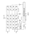
第7の実施形態
図35は、本発明に係る電圧制御発振回路の第7の実施形態を示す回路図である。図示のように、本実施形態の電圧制御発振回路では、複数の遅延段がリング状に接続されてリング発振回路が構成されている。
【0272】
遅延回路、電圧制御遅延回路または電圧制御発振回路では、遅延時間、あるいは発振周波数を広い範囲に対応するためなどで、遅延段の段数を可変にすることがしばしば行われている。このような場合、段数の切り替え回路およびその前後には、制御電圧やバイアス電圧の制御を受けないバッファ、論理ゲートまたはトランスミッションゲートが集中して配置されている。
【0273】
図35に示すように、この例では、Bタイプ遅延段によって構成されている切り替え回路が設けられている。当該Bタイプ遅延段は、例えば、バッファまたは論理ゲートによって構成され、外部から入力される切り替え制御信号に応じて、切り替えを行い、リング発振回路に組み込まれている遅延段の数を切り替えることによって、リング発振回路の発振周波数を切り替える。
【0274】
切り替え回路として設けられているBタイプ遅延段は、制御電圧あるいはバイアス電圧Vcntn, Vcntpの制御を受けないので、電源ノイズの影響を受けて、遅延時間が変化してしまうことがある。このため、遅延回路全体の遅延時間の電源電圧依存性を抑制するために、図35に示すように、Bタイプ遅延段の前後に、異なる電源電圧依存性を持つ他の遅延段、例えば、Cタイプ遅延段が配置され、電圧電圧が変化した場合、これらの遅延段の遅延時間の変化が互いに打ち消すように設計されることによって、遅延回路全体の遅延時間の電源電圧の依存性を低減できる。
【0275】
制御電圧の制御を受けないBタイプ遅延段の前後に、異なる電源電圧依存性を持つ他の遅延段を接続されている回路部分では、不感時間が生じることがある。以下、図36、37及び38を参照しつつ、ラグリードフィルタを用いたPLL回路における不感時間について説明する。
【0276】
図36はラグリードフィルタを用いたドットクロック発生用のPLL回路の一例を示す回路図である。なお、ここで、ドットクロックは、例えば、テレビモニタに通常の映像画面に重畳して文字などの情報を表示するために用いられるクロック信号である。このクロック信号は、映像信号を表示するための水平同期信号に同期する必要があるので、通常、水平同期信号を基準クロックとして、PLL回路によって生成される。
【0277】
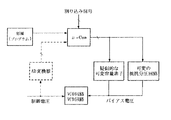
図36に示すPLL回路は、位相比較器10、チャージポンプ回路20−1,20−2、フィルタ30、電圧制御発振器(VCO)40及び分周器50によって構成されている。
分周器50は、VCO40によって生成されるクロックFout を分周比設定信号SN に応じて設定された分周比Nで分周し、分周信号Nout を出力する。
位相比較器10は、基準クロック信号としての水平同期信号Hsyncと分周信号Nout の位相を比較し、これらの信号の位相差に応じて、アップ信号SUPまたはダウン信号SDWを出力する。
チャージポンプ回路20−1,20−2は、位相比較器10から出力されるアップ信号SUPまたはダウン信号SDWに応じて、電流Icp1 とIcp2 を生成し、フィルタ30に供給する。
【0278】
フィルタ30は、図示のように、ラグリードフィルタによって構成されている。キャパシタC1の容量値は、キャパシタC2より十分大きく、即ちC1≫C2である。キャパシタC1は、例えば、外付けである。
フィルタ30によって、チャージポンプ回路20−1と20−2の出力電流に応じて、制御信号Vcnt が生成される。
VCO40は、制御信号Vcnt によって制御された発振周波数で発振し、発振信号Fout を出力する。
【0279】
なお、図示していないが、ドットクロック信号は、例えば、PLL回路の出力信号Fout を受けて、水平同期信号Hsyncの立ち下がりエッジに同期させて分周を開始する分周器によって発生する。
【0280】
図37に、ラグリードフィルタの動作時の信号波形を示す波形図である。基準クロック信号としての水平同期信号Hsyncの立ち上がりエッジと分周器の出力信号Nout の立ち下がりエッジの位相差を位相比較器で検出して、チャージポンプ回路を駆動するアップ信号SUPまたはダウン信号SDWを発生する。水平同期信号Hsyncの立ち上がりエッジより分周信号Nout の立ち下がりエッジが遅れているときは、アップ信号SUPを発生して、水平同期信号Hsyncの立ち上がりエッジよりも分周信号Nout の立ち下がりエッジが先行しているときは、ダウン信号SDWを発生して、同時のときはどちらも発生しない。
【0281】
ここで、水平同期信号Hsyncの周期をT、アップ信号SUPまたはダウン信号SDWの幅(PLLのジッタ)をΔTとする。ラグリードフィルタの出力電圧Vcntには、抵抗素子Rに生じた電圧変化分S1と、キャパシタC1に生じた電圧変化分S2が含まれている。
抵抗素子Rに生じた電圧変化分S1は、アップ信号SUPまたはダウン信号SDWが発生されたΔTの期間に、抵抗RにIcp1 の電流が流れることによって、ΔV1 =Icp1 ×Rの電圧変化が発生するパルス状の信号S1 =V1 ×ΔTの変化である。
キャパシタC1に生じた電圧変化分S2は、ΔTの時間だけ(Icp1 +Icp2)の電流が流れた分の電荷量がアップ信号SUPまたはダウン信号SDWが終了した後も(C1 +C2 )≒C1 のキャパシタに残っていることによるΔV2 ≒(Icp1 +Icp2 )×ΔT/(C1 +C2 )の電圧変化が(T±α)≒Tの期間続く、時間軸に沿って細長いS2 ≒V2 ×Tの変化である。
【0282】
ラグリードフィルタ30においては、位相引込は角速度の変化(∝周波数の変化∝制御電圧の変化)×時間で行なわれるので、S1 とS2 の和より行なわれるが、周波数の引込は、周波数の変化(∝制御電圧の変化)で行なわれるので、電圧変化が元に戻ってしまうS1 は関係なくなり、元に戻らないS2 のみにより行なわれる。
【0283】
したがって、(S1 +S2 )/S2 ∝位相修正量/周波数修正量となり、水平同期信号Hsyncの周波数が変化しても、S1 とS2 の比を一定に保つように設定することによって、PLL回路が安定した動作が得られる。
【0284】
すなわち、図36に示したPLL回路では、外付けコンデンサC1 の容量値は固定でも、分周器の分周比Nを水平同期信号Hsyncの周期Tに正比例して設定し、チャージポンプ回路20−1の出力電流Icp1 を固定して、チャージポンプ回路20−1とチャージポンプ回路20−2の出力電流値の和(Icp1 +Icp2 )を水平同期信号Hsyncの周期Tに反比例して設定することで、(S1 +S2 )/ΔT ∝位相引込量/位相のずれ量の比(=1回にどの位の割合で修正するか)、および、(S1 +S2 )/S2 ∝位相引込量/周波数引込量の比が一定になり、安定した特性を得ることが可能である。また、VCO40は、ほとんど一定の周波数で動作すれば良い。
【0285】
大規模集積回路に搭載した場合、ΔV1の電圧は、数百mVよりは大きくできないので、固定の電圧にするか2〜3倍可変にするか位の選択しかできない。したがって、Icp1 を固定の電流値とし、粗いロック検出と細かいロック検出ができる場合、S2すなわちIcp2 が周波数引込に関係して、(S1+S2)すなわち(Icp1 +Icp2 )が位相引込に関係するので、水平同期信号Hsyncの周波数が変化して粗いロック検出基準からはずれたら、Icp2 を増加させてS2 >S1の関係にすることで周波数引込時間を短縮することが可能である。
粗いロック検出基準を満足したらIcp2 を減少させてS2 ≒S1 の関係にして、位相引込を行なう。細かいロック検出基準も満足したら、周波数はほとんど補正する必要がなくなるのでIcp2 をさらに減少させてS2 <S1 の関係にして、PLL回路のフィードバックループの遅れによる過剰な周波数補正を低減することができる。
【0286】
図38に、デジタルの電源ノイズに対するラグフィルタとラグリードフィルタの応答波形を比較して示す。ラグフィルタにおいては、S1に相当する部分がなく、S2に相当するS2’のみである。
【0287】
ラグフィルタとラグリードフィルタの位相引込量を同じ(S1 +S2 =S2 ’)に考えた場合、Icp1 +Icp2 =Icp2'のときは、ΔT’=2ΔTであり、ラグリードフィルタはラグフィルタの半分のジッタ量になる。また、2×(Icp1+Icp2 )=Icp2'のときは、ΔT’=ΔTであるが、2ΔVcnt =ΔVcnt'であり、ラグフィルタでは、制御電圧の変動が2倍になってしまう。すなわち、ラグフィルタでは、S1 に相当する部分がないため、デジタルの電源ノイズの影響が本来発生して欲しくない制御電圧の変動として多く残ってしまい、結局ジッタ量が大きくなってしまう。
【0288】
S1部分は元々位相比較器のアップ信号SUP、またはダウン信号SDWとして発生されるので、位相比較器の不感帯という問題を含んでいる。したがって、位相比較器の出力で、ジッタの目標値以下のパルス幅であっても、チャージポンプ回路、ループフィルタ、バイアス回路などを経て、VCO回路あるいはVCD回路に辿り着いたときに、初めとほぼ同じパルス幅か、やや広がったパルス幅で辿り着かなければ、S1部分の有効性が得られなくなってしまうし、S2の面積も小さくなってしまい、ジッタが大きくなってしまう。
【0289】
以上の説明により、ラグリードフィルタにおけるS1部分はデジタルの電源ノイズに対して有効である。
ところで、S1 部分を受け取る方のVCO回路やVCD回路にも、位相比較器の不感帯と同じ問題がある。
図39に一般的なインバータ型の電圧制御発振器の回路例を示す。従来、広い発振周波数範囲に対応するためなどで、遅延段の段数を可変にすることが、しばしば行なわれていた。このような場合、段数の切り替え回路およびその前後には、制御電圧やバイアス電圧の制御を受けない、バッファやトランスミッションゲートや論理ゲートが集中している。たまたま、制御電圧やバイアス電圧が絡まない部分が動作しているときに、運悪くS1 部分の変化が発生するように設計してしまうと、S1 部分の幅が小さいときには、S1 部分の位相引込の効果は得られなくなり、ジッタが大きくなってしまうことが考えられる。
【0290】
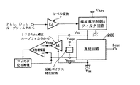
図35に示す本実施形態の電圧制御発生回路では、本発明の電源ノイズの影響を低減する方法の効果を有効に引き出すために必要な電圧制御発振器や電圧制御遅延回路における不感時間を示している。制御電圧やバイアス電圧の制御を受けない、バッファやトランスミッションゲートや論理ゲートがある部分については、それらを連続した遅延時間がジッタ量の目標値よりも十分小さく設計する必要がある。これによって、例えば、この電圧制御発振回路を用いて、図36に示すPLL回路を構成することで、電源電圧の依存性を低減でき、安定した発振周波数を持つ発振信号を得ることができ、安定したドットクロック信号を提供することができる。
【0291】
第8の実施形態
本実施形態では、本発明の遅延回路、電圧制御遅延回路または電圧制御発振回路の応用例を示す。
【0292】
第1の応用例
図40は、本発明の遅延回路の一応用例を示す回路図である。
この応用例は、本発明の遅延回路を用いた遅延時間調整回路である。図示のように、この遅延時間調整回路は、遅延回路60、バイアス回路70及び遅延時間選択回路80によって構成されている。
【0293】
遅延時間調整回路は、半導体チップ内で、データ信号とクロック信号のタイミングがずれてしまったときなどに、タイミングを調整するために使われる回路である。半導体チップの出力ピンに接続されている出力バッファは、大きな負荷容量を駆動するため、動作時に大きな電源ノイズが発生する。このような電源ノイズにより遅延調整調整回路のタイミングの調整量が狂ってしまうことがある。本発明を応用すれば電源ノイズによる調整量の狂いを低減できる。
【0294】
遅延回路60は、例えば、上述した本発明の遅延回路であり、電源ノイズ対策が施された複数のインバータ型遅延段からなる遅延回路である。入力信号Sinに対して、所定の遅延時間で遅らせた遅延信号を出力する。なお、遅延回路60は、例えば、入力信号Sinに対して異なる遅延時間Δτ1 ,…,Δτn を与えた複数の遅延信号を出力する。
バイアス回路70は、バイアス電圧Vcnt を生成し、遅延回路60の各遅延段に供給する。さらに、バイアス回路70は、各遅延段の遅延時間がほぼ一定となるように、電源電圧Vddの変動ΔVddに応じてバイアス電圧Vcnt のレベルを制御する。これによって、遅延回路60の遅延時間Δτ1 ,…,Δτn は、電源電圧の依存性が低減される。
遅延時間選択回路80は、外部から入力される選択信号SELに従って、遅延回路60から出力される複数の遅延信号のうち、所定の遅延信号を選択して出力する。
【0295】
上述したように、この遅延時間調整回路よれば、電源電圧Vddの変動による影響を抑制でき、安定した遅延時間を得られるので、電源ノイズによる遅延時間調整量の狂いを低減できる。
【0296】
第2の応用例
図41は、本発明の電圧制御発振回路(VCO)の一応用例を示す回路図であり、本発明のVCOを用いて構成されたPLL回路の回路図である。
図示のように、本例のPLL回路は、位相比較器10、チャージポンプ回路20、フィルタ30、VCO40及び分周器50によって構成されている。
【0297】
なお、図41に示すように、本応用例のPLL回路は、従来のPLL回路とほぼ同じ構成を有する。ただし、本発明のVCOを用いることによって、位相比較器10、チャージポンプ回路20またはフィルタ30は、従来のものと同じであっても、PLL回路が引き込み後電源ノイズに起因するジッタを著しく低減できる効果が得られる。
【0298】
ただし、本発明の効果は様々な条件がうまくかみ合った場合に得られるため、広い制御電圧範囲、広い発振周波数範囲で用いる電圧制御遅延回路や電圧制御発振器にはあまり向いていない。また、基本形がインバータ型のため、数百MHzまでの用途で使用できる。
【0299】
第3の応用例
図42は、本発明の電圧制御遅延回路(VCD)を応用したDLL(Delay Locked Loop )の一例を示す回路図である。図示のように、このDLLは、位相比較器10、チャージポンプ回路20、フィルタ30、VCO40a及び2分周器50aによって構成されている。
【0300】
2分周器50aは、外部から入力される基準クロック信号CKref を2分周した分周信号CK1を位相比較器10に供給する。
VCD40aは、フィルタ30から出力される制御信号Vcnt に応じて遅延時間が制御される。そして、制御された遅延時間で入力信号CK1を遅らせて、遅延信号SD を出力する。
位相比較器10は、クロック信号CK1とVCO40aによって出力された遅延信号SD の位相を比較し、これらの信号の位相差に応じてアップ信号SUPまたはダウン信号SDWの何れかを出力する。
【0301】
本応用例において、位相比較器10、チャージポンプ回路20及びフィルタ30は、従来のものによって構成されている。即ち、位相比較器10の位相比較結果に応じて、チャージポンプ回路20及びフィルタ30によって、分周クロック信号CK1と遅延信号SD との位相差に応じた制御信号Vcnt が生成され、VCD40aに供給される。
このため、VCD40aの遅延時間Δτは、分周クロック信号CK1と遅延信号SD の位相差に応じて制御される。この結果、VCD40aから、分周クロック信号CK1に位相が同相する発振信号SD を獲得できる。
【0302】
本応用例のように、本発明のVCDを用いて構成されたループ発振回路によって、入力される基準クロック信号CKref に位相同期する信号を提供できる。さらに、本発明のVCDを用いることによって、VCDの遅延時間が電源電圧Vddの変動による影響を低減でき、安定した発振信号を提供できる。
【0303】
第3の応用例
図43は、本発明のVCOを用いて構成されたPLL回路及びこのPLL回路を含むドットクロック発生回路の回路図である。
本例のドットクロック発生回路は、例えば、デジタルTV用のドットクロックとVBIサンプリングクロックを発生する発生回路に適用できる。PLL回路は、例えば、親画面の水平同期信号HSYNC0、または子画面の水平同期信号HSYNC1のうち何れかが選択された水平同期信号HSYNCを基準クロックとして、その立ち上がりエッジ(画面の右端に対応する)で分周器出力と同期をとり、画面右端においてチャージポンプ回路が動作する。
【0304】
図示のように、PLL回路部分は、位相比較回路10、チャージポンプ回路20、フィルタ30、VCO40、分周器50及びバイアス回路70によって構成される。PLL回路のほかに、制御回路400、VBIサンプリングクロック発生回路410及びドットクロック発生回路420と430が設けられ、これらの回路によって、ドットクロックを生成するドットクロック生成回路が構成される。
【0305】
PLL回路部分において、インバータ型VCO回路に本発明の電源ノイズの影響を受けにくい電圧制御発振器を用いることで低ジッタのPLL回路を実現している。ドットクロック発生回路420及び430は、VCO回路の出力クロック信号Sout を受けて、水平同期信号のバッファ信号HSYNC0B、HSYNC1Bの立ち下がりエッジ(画面左端)に同期させてドットクロック信号を発生する。
【0306】
図44は、本応用例のドットクロック生成回路が動作するシステムの電源ノイズを示す波形図である。本例のドットクロック生成回路は、図44(a)に示す水平同期信号Hsyncを基準クロックとして、ドットクロック信号を生成する。図44(b)、(d)、(e)及び(f)は、それぞれ電源電圧Vddに混入されるディジタルノイズ、画像表示系ノイズ、サーボ系ノイズ及びモーターノイズを示している。本応用例において、電源ノイズに対策が施されたVCOを用いてPLL回路を構成することによって、電源電圧Vddに混入される様々なノイズによる影響を低減でき、安定した周波数を持つドットクロック信号を生成することができる。
【0307】
電源ノイズの影響を受けにくいVCO回路の採用と、水平同期信号への同期方法の工夫により、高逓倍のPLL回路にもかかわらず、電源電圧Vddの変動による影響を抑制でき、安定した周波数を持つドットクロック信号を生成できるので、表示画面上に安定したOSD文字を表示でき、フリッカーやウェービングが見えない表示を得られている。
【0308】
【発明の効果】
以上説明したように、本発明の遅延回路、電圧制御遅延回路及び電圧制御発振回路によれば、電源ノイズの影響を抑制でき、低ジッタのPLL回路、DLL回路が実現できる。
また、本発明に係る電圧制御発振回路は、半導体チップに内蔵しても十分なジッタ特性が得られるため、パソコンの映像信号の表示やTVのOSD文字の表示用のドットクロック信号の発生源として用いることができる。このため、セット上の部品点数を削減できる。
また、半導体チップに内蔵することで、分周比の設定も基準クロックの周波数に合わせて変更できるなど様々な制御が可能になるため、デジタル放送に対応したTVに使用できる。
さらに、本発明によれば、インバータ型の遅延段が遅延回路、電圧制御遅延回路または電圧制御発振回路の基本的な構成要素なので、低消費電力化または低電源電圧化を容易に実現できる。
【図面の簡単な説明】
【図1】本発明に係る遅延回路、電圧制御遅延回路または電圧制御発振回路の第1の実施形態を示す概念図である。
【図2】本発明の第1の実施形態の構成図である。
【図3】本発明の第1の実施形態の第1の回路例を示す回路図である。
【図4】インバータ型遅延段で構成された遅延部の回路図である。
【図5】インバータ型遅延段で構成された遅延部の動作を示す波形図である。
【図6】バイアス回路と交流加算手段の構成及び等価回路を示す図である。
【図7】電源ノイズの影響を同じ割合で伝える直流加算手段と交流加算手段を示す回路図である。
【図8】本発明の第1の実施形態の第1の回路例のシミュレーション結果を示す図である。
【図9】本発明の第1の実施形態の第2の回路例を示す回路図である。
【図10】本発明の第1の実施形態の第3の回路例を示す回路図である。
【図11】シャント型遅延段で構成されている遅延部の回路図である。
【図12】シャント型遅延段で構成されている遅延部の動作を示す波形図である。
【図13】本発明の第2の実施形態の概念を示す図である。
【図14】本発明の第2の実施形態の構成図である。
【図15】本発明の第2の実施形態の第1の回路例を示す回路図である。
【図16】本発明の第2の実施形態の第2の回路例を示す回路図である。
【図17】本発明の第2の実施形態の第3の回路例を示す回路図である。
【図18】本発明の第2の実施形態の第3の回路例の他の構成例を示す回路図である。
【図19】本発明の第2の実施形態の第3の回路例の別の構成例を示す回路図である。
【図20】本発明の第2の実施形態の第3の回路例のシミュレーション結果を示す図である。
【図21】本発明の第3の実施形態を示す構成図である。
【図22】本発明の第3の実施形態の他の構成例を示す図である。
【図23】しきい値補正抵抗分圧回路の構成を示す回路図である。
【図24】本発明の第4の実施形態を示す構成図である。
【図25】本発明の第5の実施形態を示す構成図である。
【図26】可変容量素子の構成を示す回路図である。
【図27】疑似的な可変容量素子の回路例を示す回路図である。
【図28】一般的な電圧制御発振回路の一構成例を示す回路図である。
【図29】本発明の第6の実施形態の第1の回路例を示す回路図である。
【図30】本発明の第6の実施形態の第1の回路例の原理を示す図である。
【図31】本発明の第6の実施形態の第2の回路例を示す回路図である。
【図32】本発明の第6の実施形態の第2の回路例の原理を示す図である。
【図33】本発明の第6の実施形態の第3の回路例を示す回路図である。
【図34】本発明の第6の実施形態の第3の回路例の原理を示す図である。
【図35】本発明の第7の実施形態をの構成を示す回路図である。
【図36】ラグリードフィルタを用いてPLL回路の回路例を示す回路図である。
【図37】ラグリードフィルタの動作を示す波形図である。
【図38】電源ノイズに対するラグフィルタとラグリードフィルタの応答波形を示す波形図である。
【図39】一般的なインバータ型の電圧制御発振回路の回路例を示す回路図である。
【図40】本発明の第1の応用例である遅延時間調整回路の構成を示す回路図である。
【図41】本発明の第2の応用例であるPLL回路の構成を示す回路図である。
【図42】本発明の第3の応用例であるDLL回路の構成を示す回路図である。
【図43】本発明の第4の応用例であるドットクロック発生生成回路の構成を示す回路図である。
【図44】本発明の第4の応用例の動作を示す波形図である。
【図45】従来の高逓倍PLL回路におけるジッタ量と基準クロック周期との関係を示すグラフである。
【符号の説明】
10…位相比較器、20…チャージポンプ回路、30…フィルタ、40…電圧制御発振回路(VCO)、40a…電圧制御遅延回路、60…遅延回路、70…バイアス回路、80…遅延時間選択回路、100,100a,100b,100c,200,200a,200b…遅延部、110,112,114,116,110−1,…,110−j…交流加算回路、130,132…直流加算回路、140,142,142a…基準電圧発生回路、150,152…直流分圧回路、160,162…疑似的な可変容量素子、170…参照電圧発生回路、300a,300b,300c1,300c2…遅延部、400…制御回路、410…VBIサンプリングクロック発生回路、Vdd…電源電圧、VSS…基準電位。[0001]
BACKGROUND OF THE INVENTION
The present invention relates to a delay circuit, for example, a delay circuit having a stable delay time without being influenced by noise of a power supply voltage, a voltage control delay circuit capable of controlling a delay time according to a control voltage, and a control voltage The present invention relates to a voltage controlled oscillation circuit capable of controlling the oscillation frequency according to the above, a delay adjustment circuit using a delay circuit, a DLL (Delay Locked Loop) circuit, and a PLL (Phase Locked Loop) circuit.
[0002]
[Prior art]
The delay time of the delay circuit or the voltage control delay circuit fluctuates when power supply noise exists such as when the power supply voltage fluctuates. Further, in an oscillation circuit configured by connecting a plurality of delay circuits in a ring shape, a voltage controlled oscillation circuit (VCO) can be configured by controlling the delay time of each delay circuit in accordance with the control voltage. . When power supply noise occurs, the delay time of the delay circuit changes, so the oscillation frequency of the VCO also changes accordingly.
[0003]
In a PLL circuit configured by a phase comparison circuit, a loop filter, a VCO, and the like, fluctuations in the oscillation frequency of the VCO can be reduced by feedback control. That is, when the oscillation frequency of the VCO changes due to power supply noise, the phase comparison circuit detects the phase or frequency deviation of the oscillation signal, generates a control signal according to the detection result of the phase deviation, and corrects the oscillation frequency of the VCO. As a result, the phase and frequency deviation of the oscillation signal caused by the influence of power supply noise can be corrected to some extent, and the occurrence of jitter due to power supply noise can be suppressed.
[0004]
The horizontal sync signal H is used to display video signals on personal computers (PCs) and OSD (On Screen Display) characters on TV monitors.syncIs used as a reference clock to generate a dot clock signal multiplied by a PLL circuit, and graphic data and character data are displayed by this dot clock signal. If the jitter of the PLL circuit is not so small, it will be caught visually as flicker or waving on the screen. For example, if only 24 dots / character × 32 characters = 768 dots are displayed in the horizontal direction, the effective horizontal period is 70%, and the allowable jitter amount is ± 1/8 dot, the cycle of the horizontal sync signal is about ± 1 /. It is necessary to suppress the jitter amount to (768 ÷ 0.7 × 8) = ± 1/8777. Horizontal sync signal frequency fH The standard of the jitter amount when = 15.734 kHz is ± 7.2 ns, and the frequency f of the horizontal synchronizing signalH The standard of the jitter amount when = 47.250 kHz is ± 2.4 ns. The frequency f of the horizontal synchronizing signalH The standard of the jitter amount when = 106.250 kHz is ± 1.1 ns.
[0005]
The target value of the jitter amount described above seems to be easily satisfied. However, in the case of a high-multiplication PLL circuit, the reference clock period of the PLL circuit is set to Tref , Frequency fref Then Tref The influence of digital noise that occurs at a much shorter period is corrected in the feedback loop of the PLL circuit for the average value portion, and the variation from the remaining average value affects the jitter amount.
Tref As the length becomes longer, the variation part is added.j (Tj ∝√Tref = 1 / √fref ) Is presumed to hold.
[0006]
FIG. 45 shows the relationship between the target value of the jitter amount and the ability of the PLL. As shown in the figure, the frequency f of the horizontal synchronizing signalH Even if the target value is cleared at 15.734 kHz, fH = 47.250 kHz or fH When = 106.250 kHz, the target value cannot be cleared.
That is, fref = Jitter amount at 100 kHz is fref = It is estimated that the jitter amount is 14 times that at 20 MHz, and the actual jitter amount is further increased. Therefore, the design of a PLL circuit with a very high multiplication factor of several thousand to 10,000 times is as follows. It has become very difficult.
[0007]
There are many video signal standards for video signals of personal computers, and the horizontal synchronization signal must correspond to a frequency band of 31.436 kHz to 106.250 kHz.
Also, with respect to television monitors, various specifications have come into existence with the spread of digital broadcasting, and horizontal synchronization signals must correspond to a frequency band of 12.8757 kHz to 47.250 kHz.
[0008]
Such a versatile PLL circuit has a horizontal synchronizing signal frequency f.H It is necessary to change the characteristics of the filter according to the requirements, but since it cannot be done by changing the external parts, the PLL circuit is built in the semiconductor integrated circuit except for some parts, and the program It is better to design so that it can be changed.
In order to be incorporated in a semiconductor integrated circuit, a PLL circuit that hardly generates jitter even when receiving noise from other digital circuits is required.
[0009]
Since the design of the PLL circuit has been performed by solving the characteristic equation of the feedback loop, the technology for reducing the jitter of the PLL and DLL is a technology (such as variable filter characteristics) for achieving both high-speed pull-in and low jitter. Has been centered.
In order to realize low jitter, it is considered from the characteristic equation that it is better to reduce the gain of the PLL circuit. However, if the gain of the PLL circuit is reduced, the problem and process that the pull-in speed is slowed down. There is a problem that it is weak against variation, and various circuit devices have been devised.
[0010]
For example, the initial control voltage of the VCO is supplied by a digital / analog converter (DAC), and the output voltage of the charge pump when the pull-in is completed is stored. Coarse control is performed by digitally changing the number of delay stages of the VCO circuit and the current supply capability of the current source transistor, and fine control is performed with an analog control voltage. Here, the digital PLL operates in the unlocked state, and the PLL operates in the locked state. The output current of the charge pump is made variable, and measures such as reducing the output current of the charge pump in the locked state are taken.
Japanese Patent Laid-Open No. 9-214340 “PLL circuit”, Japanese Patent Laid-Open No. 9-172370 “PLL circuit”, Japanese Patent Laid-Open No. 7-106959 “Phase synchronization circuit”, Japanese Patent Laid-Open No. 10-242851 “PLL circuit”, etc. An improved PLL circuit is disclosed.
[0011]
However, since the power supply voltage dependency is not incorporated in the characteristic equation of the feedback loop, it is not a general problem for a PLL circuit designer to design a circuit having a small power supply voltage dependency. For this reason, the above measures do not take into account jitter caused by power supply noise in a locked state, which is a problem in a high-multiplication low-jitter PLL used for display of a video signal of a personal computer or display of OSD characters of a television monitor. It was.
[0012]
Japanese Patent Laid-Open No. 8-288801 “Low Jitter Wide Frequency Range Voltage Controlled Oscillator” is known as a conventional technique considering the jitter caused by power supply noise in the locked state. Among them, “the output frequency generated by the voltage controlled oscillator is the control voltage VC While it is the power supply voltage V according to the inverse square root function of the supply voltage.ddFluctuates with. ... High PSRR:
[0013]
In recent years, in the field of ATM (Asynchronous Transfer Mode) communication, in order to cope with higher system clock frequency and built-in PLL and DLL chips, a PLL using a voltage-controlled oscillator using a differential delay circuit, A DLL using a voltage controlled delay circuit (VCD circuit) using a dynamic delay circuit has been developed.
The differential circuit has a good CMRR (common-mode signal rejection ratio), and if designed well, the PSRR (power supply rejection ratio) is also good, and it is strong against digital noise, which is a problem with the built-in chip. As described above, it is a general problem for a designer of a differential circuit to design a circuit having a small power supply voltage dependency.
[0014]
The differential circuit does not need to fully swing the input / output signal and can operate at a high speed. However, the output amplitude is not constant because the full swing is not performed, and the delay time is likely to vary. In order to solve this problem, a clamp circuit and a feedback circuit that make the output amplitude of the VCO circuit and the VCD circuit constant are provided, and a low jitter PLL and DLL have been developed. In addition, replacing the current source transistor connected to the current line side with a source follower transistor makes it difficult for the effects of power supply fluctuations to be transmitted to the differential transistor, and a method of controlling the oscillation frequency with the gate input voltage of the source follower is also conceivable. ing.
[0015]
For differential circuits, see Masayuki MIZUNO, et al., “Low-Power and High-Speed LSI Technologies. A 0.18−μm CMOS Hot-Standby PLL Using a Noise-Immune Adaptive-Gain VCO”, IEICE Trans. Electron (Inst Electron Inf. Commun. Eng.) VOL. E80-C, NO. 12; PAGE, 1560-1571; 1997; and Japanese Patent Application Laid-Open No. 9-214299 “Voltage Controlled Oscillator” and related documents. Takehiko Nakao, et al., “Single-Chip 4-Channel 155Mb / s CMOS LSI Chip for ATM SONET / SDE Framing and Clock / Data Recovery”, Dig. Tech. Pap. IEEE Int. Solid State Circuits COnf. VOL. 40 ; PAGE. 160-161, 448; detailed in 1997.
[0016]
[Problems to be solved by the invention]
By the way, in the above-described differential type PLL circuit and DLL circuit, both D and / D transistors operate. For this reason, the current consumption and the layout area are about twice that of the non-differential circuit. Since the input / output signals do not need to be fully swung, the speed is increased. For example, if it is sufficient to swing only about half the amplitude, the speed will be doubled. However, since it is necessary to attach a clamp circuit or a feedback circuit, there is a disadvantage that the current consumption further increases and the speed cannot be as high as expected. In addition, when an output signal is taken out, a signal that is not fully swung must be converted to a signal that is fully swung, so the duty is likely to be distorted, and the differential circuit has a large number of stages of transistors connected in the vertical direction. In order to reduce the power supply voltage, it is necessary to devise to secure an operation margin. For this reason, the differential PLL circuit and the DLL circuit have many technical problems.
[0017]
The present invention has been made in view of such circumstances, and an object of the present invention is to control the drive current supplied to the inverter-type delay element, or to use a delay element having different power supply voltage dependency, thereby providing a circuit configuration. It is possible to provide an inverter type delay circuit, a voltage controlled oscillation circuit, a voltage controlled delay circuit, a delay adjustment circuit, a DLL circuit, and a PLL circuit that can reduce the influence of power supply noise and reduce jitter. .
[0018]
[Means for Solving the Problems]
In order to achieve the above object,According to the first aspectThe delay circuitVoltage level is controlledA delay stage in which the drive current is controlled according to the bias voltage and the delay time is determined by the drive currentWhen,Power supply voltage fluctuation at a predetermined rateSaidAdd to the bias voltage and add the resultSaidAdding means for supplying to delay stageWhenHave
[0019]
A delay adjustment circuit according to a second aspect of the present application is a delay adjustment circuit that outputs a delay signal obtained by giving a predetermined delay time to an input signal, and includes a bias circuit that generates a bias voltage, and the bias voltage according to the bias voltage. A delay circuit that delays the input signal by a plurality of controlled different delay times and outputs a plurality of delay signals, and any one or some of a plurality of delay signals output from the delay circuit according to a selection signal The delay circuit is the delay circuit according to the first aspect.
[0020]
In the voltage controlled delay circuit according to the third aspect of the present application, the driving current is controlled according to the control voltage whose voltage level is controlled, the delay stage whose delay time is determined by the driving current, and the fluctuation of the power supply voltage are predetermined. And adding means for adding the result to the delay stage.
[0021]
A DLL circuit according to a fourth aspect of the present application compares a phase of an input signal and a delay signal, outputs a phase difference signal corresponding to the comparison result, and a control voltage according to the phase difference signal. And a voltage control delay circuit that delays the input signal by a delay time controlled according to the control voltage and outputs the delay signal, and the voltage control delay circuit includes: It is a voltage control delay circuit concerning the 3rd mode.
[0022]
In the voltage controlled oscillation circuit according to the fifth aspect of the present application, a drive current is controlled according to a control voltage whose voltage level is controlled, and a delay stage whose delay time is determined by the drive current is connected in a ring shape. The control oscillation circuit includes addition means for adding a change in power supply voltage to the control voltage at a predetermined rate and supplying the addition result to the delay stage.
[0023]
A PLL circuit according to a sixth aspect of the present application compares a phase of a reference signal and an oscillation signal, outputs a phase difference signal according to the comparison result, and a control voltage according to the phase difference signal. And a voltage controlled oscillation circuit that oscillates at an oscillation frequency controlled in accordance with the control voltage and outputs the oscillation signal, wherein the voltage controlled oscillation circuit is in a fifth mode. This is a voltage-controlled oscillation circuit.
[0024]
Each of the above aspects includes the following preferred aspects.
Preferably, the adding means may include AC adding means for adding an AC component included in the fluctuation amount of the power supply voltage to the bias voltage.
Preferably, the AC adding means includes a first capacitor connected between the power supply voltage supply line and the bias voltage supply line, and the bias voltage supply line and the reference voltage (GND). You may have the 2nd capacitor connected between supply lines.
[0025]
Preferably, the delay stage is a plurality of delay stages connected between a power supply line and a reference potential line, and each of the plurality of delay stages includes a delay element including a switching transistor or a selector transistor. A current source transistor that supplies a driving current to the delay element, and control terminals of the plurality of current source transistors in the plurality of delay stages are connected to a control line for controlling the driving current, The bias voltage whose voltage level is controlled is input to the first control line, the first capacitor is connected between the control line and the power supply line, and the second capacitor is the control line. A plurality of current source transistors connected between the first capacitor and the second capacitor. In portions of the end side of the control line, is connected to the control line, the end of the control line may be terminated in any one of the current source transistor of the plurality of current source transistors.
[0026]
Preferably, a first resistance element is connected between the control line and the power supply line, a second resistance element is connected between the control line and the reference potential line, and the plurality of current sources The transistor may be connected to the control line at a portion closer to the end of the control line than the first resistance element and the second resistance element.
[0027]
Preferably, at least one of the first capacitor and the second capacitor may be a variable capacitor.
[0028]
Preferably, the adding means may include a DC adding means for adding a DC component included in the fluctuation amount of the power supply voltage to the bias voltage.
Preferably, the DC adding means includes a first resistance element connected between the power supply voltage supply line and the bias voltage supply line, the bias voltage supply line, and a reference voltage supply line. And a second resistance element connected between them.
[0029]
Preferably, the delay stage includes a MOS inverter, a first current source transistor connected between the inverter and the power supply voltage supply line, and a first bias voltage applied to a gate; A second current source transistor connected between the inverter and the reference voltage supply line and having a gate to which a second bias voltage is applied may be included.
[0030]
Preferably, the MOS type inverter may be an inverter having a differential configuration in which the first current source transistor and the second current source transistor are current source transistors.
[0031]
Preferably, the adding means is included in first AC adding means for adding an AC component included in the fluctuation amount of the power supply voltage to the first bias voltage, and included in the fluctuation amount of the power supply voltage. And a second alternating current adding means for adding the alternating current component to the second bias voltage.
Preferably, the AC adding means includes a first capacitor connected between the power supply voltage supply line and the bias voltage supply line, and the bias voltage supply line and the reference voltage (GND). You may have the 2nd capacitor connected between supply lines.
[0032]
Preferably, the adding means is included in first power DC voltage adding means for adding a DC component included in the power supply voltage fluctuation amount to the first bias voltage, and in the power supply voltage fluctuation quantity. And a second direct current adding means for adding the direct current component to the second bias voltage.
[0033]
Preferably, the delay stage includes a MOS inverter, a plurality of first current source transistors each having one terminal connected to the power supply voltage supply line and a gate to which a first bias voltage is applied. Are connected to a reference voltage supply line, and are connected between a plurality of second current source transistors having a gate to which a second bias voltage is applied, and between the first current source transistor and the inverter, A first switching circuit that selects and supplies any or some of the output currents of the plurality of first current source transistors to the inverter, and is connected between the second current source transistor and the inverter. And a second switching circuit that selects and supplies any or some of the output currents of the plurality of second current source transistors to the inverter.
Preferably, the MOS type inverter may be an inverter having a differential configuration in which a plurality of first current source transistors and a plurality of second current source transistors are current source transistors.
Preferably, the AC adding means includes a first capacitor connected between the power supply voltage supply line and the bias voltage supply line, and the bias voltage supply line and the reference voltage (GND). You may have the 2nd capacitor connected between supply lines.
[0034]
Preferably, the delay stage includes a MOS inverter, a switching transistor in which one terminal is connected to an output terminal of the inverter, the bias voltage is applied to a gate, and one electrode is the other of the switching transistors. A capacitor connected to the terminal and having the other electrode connected to a reference voltage supply line.
Preferably, the adding means includes a capacitor connected between the power supply voltage supply line and the bias voltage supply line and coupling an AC component of the fluctuation of the power supply voltage to the bias voltage. Also good.
[0035]
Preferably, the delay stage is a plurality of delay stages connected between a power supply line and a reference potential line, and each of the plurality of delay stages includes a delay element including a switching transistor or a selector transistor. A current source transistor for supplying a driving current to the delay element, and a control terminal of the plurality of current source transistors in the plurality of delay stages has a first control line or a second control line for controlling the driving current. The bias voltage for controlling the voltage level is input to the first control line and the second control line, which are alternately connected to the control line, and the adding means is connected to the first control line and the power supply line. A plurality of current sources including a first capacitor connected between the second capacitor and a second capacitor connected between the first control line and the reference potential line. The transistor is connected to the first control line at a portion closer to the end of the first control line than the first capacitor and the second capacitor, and the end of the first control line is connected to the plurality of current source transistors. And a third capacitor is connected between the second control line and the power supply line, and a fourth capacitor is connected between the second control line and the reference potential line. A capacitor is connected, and the plurality of current source transistors are connected to the second control line at a portion closer to the end of the second control line than the third capacitor and the fourth capacitor, and the second control line May be terminated at any one of the plurality of current source transistors.
[0036]
Preferably, the delay stage is a plurality of delay stages connected between a power supply line and a reference potential line, and each of the plurality of delay stages includes a delay element including a switching transistor or a selector transistor. A power source side current source transistor that is connected between the power supply line and the delay element and supplies a drive current to the delay element; and connected between the delay element and the reference potential line; A reference-side current source transistor that supplies a drive current, and control terminals of the plurality of power-source-side current source transistors in the plurality of delay stages are a first control line or a second control line for controlling the drive current. The bias voltage for controlling the voltage level is inputted to the first control line and the second control line, and the adding means A first capacitor connected between the first control line and the power supply line; and a second capacitor connected between the first control line and the reference potential line. The side current source transistor is connected to the first control line at a portion closer to the end of the first control line than the first capacitor and the second capacitor. Terminating in any one of the power source side current source transistors, a third capacitor is connected between the second control line and the power source line, and the second control line and the reference potential line are connected to each other. A fourth capacitor is connected therebetween, and the plurality of power source side current source transistors are connected to the second control circuit more than the third capacitor and the fourth capacitor. The terminal of the second control line is connected to the second control line, and the terminal of the second control line is terminated in any one current source transistor of the plurality of power source side current source transistors. Control terminals of a plurality of reference-side current source transistors in the delay stage are alternately connected to a third control line or a fourth control line for controlling the drive current, and the third control line and the fourth control line include The bias voltage for controlling the voltage level is input, a fifth capacitor is connected between the third control line and the power supply line, and between the third control line and the reference potential line, A sixth capacitor is connected, and the plurality of reference-side current source transistors are connected to the end of the third control line with respect to the fifth capacitor and the sixth capacitor. The third control line is connected to the third control line, and the termination of the third control line is terminated in any one of the plurality of reference-side current source transistors, and the fourth control line and the A seventh capacitor is connected between the power supply line, an eighth capacitor is connected between the fourth control line and the reference potential line, and the plurality of reference-side current source transistors are connected to the seventh capacitor. And at the terminal side of the fourth control line with respect to the eighth capacitor, the terminal is connected to the fourth control line, and the terminal of the fourth control line is one of the plurality of reference-side current source transistors. It may be terminated in the current source transistor.
[0037]
Preferably, the delay stage in which the control terminal of the power source side current source transistor is connected to the first control line has the control terminal of the reference side current source transistor connected to the third control line, and the power source In the delay stage in which the control terminal of the side current source transistor is connected to the second control line, the control terminal of the reference side current source transistor may be connected to the fourth control line.
[0038]
Preferably, the plurality of power supply side current source transistors of the plurality of delay stages are connected to the power supply line between the first capacitor and the third capacitor, and the plurality of references of the plurality of delay stages The side current source transistor may be connected to the reference potential line between the second capacitor and the fourth capacitor.
[0039]
Preferably, the delay stage is a plurality of delay stages connected between a power supply line and a reference potential line, and each of the plurality of delay stages includes a delay element including a switching transistor or a selector transistor; A current source transistor that supplies a driving current to the delay element, and a control terminal of the plurality of current source transistors in the plurality of delay stages has a first control line or a second control for controlling the driving current. The bias voltage for controlling the voltage level is input to the first control line and the second control line, and the adding means is provided between the first control line and the power supply line. A first capacitor connected to the first control line and a second capacitor connected between the first control line and the reference potential line, the plurality of current source transistors. The transistor is connected to the first control line at a portion closer to the end of the first control line than the first capacitor and the second capacitor, and the end of the first control line is connected to the plurality of current source transistors. And a third capacitor is connected between the second control line and the power supply line, and the plurality of current source transistors are connected to the second capacitor more than the third capacitor. The terminal of the control line may be connected to the second control line, and the terminal of the second control line may be terminated in any one of the plurality of current source transistors.
[0040]
Preferably, the delay circuit, the voltage control delay circuit, or the voltage control oscillation circuit may be formed in a semiconductor chip, and the semiconductor chip may include an output buffer connected to an output pin of the semiconductor chip.
[0041]
DETAILED DESCRIPTION OF THE INVENTION
First embodiment
FIG. 1 is a conceptual diagram showing a first embodiment of a delay circuit according to the present invention.
As shown in the figure, the delay circuit according to the present embodiment includes a
Further, bias voltages Vcnt1 to Vcntj are supplied by a phase comparator, a charge pump circuit, a loop filter and a bias circuit which are not shown.
[0042]
The
[0043]
The AC adder circuits 110-1 to 110-j each have a power supply voltage VddAnd reference potential VSSThe results obtained by multiplying the AC component by the predetermined coefficients Kc1 to Kcj are output as ΔVc1 to ΔVcj, respectively, and the result obtained by adding the bias voltages (or control voltages) Vcnt1 to Vcntj and the outputs ΔVc1 to ΔVcj of the AC adding circuit is controlled. The voltages Vc1 to Vcj are supplied to the
[0044]
Where the reference potential VSS= 0, and the power supply voltage V added by the AC adder circuits 110-1 to 110-jddAC component of ΔVddThen, outputs ΔVc1 to ΔVcj of AC adder circuits 110-1 to 110-j are expressed by the following equations, respectively.
[0045]
[Expression 1]
The control voltages Vc1 to Vcj are obtained by the following equations, respectively.
[Expression 2]
In the
In the present embodiment, the control set including the AC addition circuit and the bias circuit is not limited to two sets, and a plurality of sets may be provided.
[0048]
The voltage V input to the delay circuit shown in the figure.cnt1, ..., VcntjFor example, if the bias voltages are held at a certain level, the delay time of the
[0049]
FIG. 2 is a circuit diagram showing a configuration example of this embodiment. As shown in the figure, the
[0050]
In the
[0051]
In the delay circuit of this embodiment, the power supply voltage VddFluctuation ΔVddIs added to the control voltage at an appropriate ratio, and the power supply voltage V is controlled so as to cancel the change in the delay time of the delay element.ddIt is possible to suppress a change in the delay time due to the fluctuation of.
The power supply noise generated during the operation of the output buffer is, for example, pulse noise, and its pulse width is at most several tens of nsec (nanoseconds). Therefore, it is effective to provide at least an AC addition circuit. can get. For power supply noise with a wider pulse width, it is better to add DC. In that case, a DC level generator in normal operation, for example, the output of a charge pump or bias circuit output and DC adding means Must be designed so that they do not compete.
[0052]
Next, for a typical current source type delay circuit among the inverter type delay circuits, the change in the delay time can be suppressed by adding the fluctuation of the power supply voltage to the control voltage and the bias voltage at an appropriate ratio. Will be described.
[0053]
First circuit example
FIG. 3 shows a first circuit example of the inverter type delay circuit of the present embodiment. As illustrated, the delay circuit includes a
[0054]
Capacitor CdpIs the power supply voltage VddAnd input terminal TcntpConnected to the capacitor CspIs the input terminal TcntpAnd reference potential VSSConnected between and. Input terminal TcntpControl voltage VcntpIs entered.
Capacitor CdnIs the power supply voltage VddAnd input terminal TcntnConnected to the capacitor CsnIs the input terminal TcntnAnd reference potential VSSConnected between and. Input terminal TcntnControl voltage VcntnIs entered.
[0055]
The
[0056]
Control voltage VcpAnd VcnAccordingly, the supply currents of the P-channel side current source and the N-channel side current source are controlled, and the delay times of the n-stage inverters INV1, INV2,..., INVn provided as delay elements are controlled accordingly. The
[0057]
The operation of the delay circuit of this example will be described below.
FIG. 4 is a circuit diagram showing the configuration of the
[0058]
In the
[0059]
In the operation waveform, from the time when the input signal level of each delay stage crosses the logic threshold voltage VthL to the time when the output signal level of each delay stage crosses the logic threshold voltage VthL (the next stage) The delay time when the output signal falls is τni, and the delay time when the output signal rises is τpi.
[0060]
Here, if the load capacitance of each delay stage output is CLi, the charge of the load capacitance CLi is extracted from Vdd to VthL by the nMOS current source transistor in the period τni when the output signal falls. Also, during the period of τpi at the time of rising of the output signal, the charge of the load capacitor CLi is stored from 0V to VthL by the PMOS current source transistor.
Therefore, the following equation is established.
[0061]
[Equation 3]
τni∝CLi × (Vdd−VthL) / Ini (3)
[Expression 4]
τpi∝CLi × VthL / | Ipi | (4)
[0062]
Here, if there is a fluctuation Vdd of the power supply voltage,
[Equation 5]
ln (τni) ∝ln (CLi) + ln (Vdd−VthL) −ln (Ini)
Δτni / τni = (ΔVdd−ΔVthL) / (Vdd−VthL) −ΔIni / Ini (5)
Therefore, the following equation is obtained.
[0063]
[Formula 6]
Δτni = τni [{(ΔVdd−ΔVthL) / (Vdd−VthL)} − (ΔIni / Ini)] (6)
[Expression 7]
Δτpi = τpi {(ΔVthL / VthL) − (Δ | Ipi | / | Ipi |)} (7)
[0064]
When the nMOS transistor and the pMOS transistor are balanced, in the equations (6) and (7), Ini = | Ipi | = ID Τni = τpi = τd and VthL≈Vdd / 2, so that the following equation is obtained.
[0065]
[Equation 8]
Δτni≈τd [{(ΔVdd−ΔVthL) / (Vdd / 2)} − (ΔIni / ID ]] ... (8)
[Equation 9]
Δτpi≈τd [{ΔVthL / (Vdd / 2)} − (Δ | Ipi | / ID ]] ... (9)
[0066]
In order to reduce the influence of power supply noise for each delay stage, Δτni≈0 and Δτpi≈0 must be set. Therefore, the following expression must be established from the expressions (8) and (9). is there.
[0067]
[Expression 10]
(ΔVdd−ΔVthL) / (Vdd / 2) ≈ΔIni / ID (10)
## EQU11 ##
ΔVthL / (Vdd / 2) ≈Δ | Ipi | / ID ... (11)
[0068]
In order to relax the conditions and reduce the influence of power supply noise for every two successive delay stages, Δτni + Δτp (i ± 1) ≈0 must be set. Therefore, from equations (8) and (9), The following equation is obtained.
[0069]
[Expression 12]
ΔVdd / (Vdd / 2) ≈ (ΔIni + Δ | Ip (i ± 1) |) / ID (12)
[0070]
The control voltages Vcntn and | Vcntp | are approximately values near Vdd / 2, and both the nMOS current source transistor and the pMOS current source transistor operate in the saturation region. Assuming that the channel length modulation effect coefficient is λn and λp, the current equation in the saturation region including the channel length modulation effect is given as follows.
[0071]
[Formula 13]
Ini = (1/2) μn Cox (Wni / Lni) (1 + λn VthL) (Vcntn−Vthn) ** 2 (13)
[Expression 14]
| Ipi | = (1/2) | μp | Cox (Wpi / Lpi) {1+ | λp | (Vdd−VthL)} (Vcntp−Vthp) ** 2 (14)
[0072]
There is no general definition for the logic threshold voltage of the inverter circuit with the current source transistor, but the voltage of the output signal of the delay stage is approximately when the voltage of the gate input signal for inverter operation is Vdd / 2. Is balanced by VthL, and it is defined that Ini = | Ipi | holds, the following equations are obtained from equations (13) and (14).
[0073]
[Expression 15]
The fluctuation ΔVthL of the logical threshold voltage can be obtained from the equation (15) as follows.
[Expression 16]
ΔVthL = {| λp | / (λn + | λp |)} ΔVdd (16)
[0075]
Ini and | Ipi | fluctuations ΔIni and Δ | Ipi | take into account that the values of λn and | λp | are small, the saturation region current equation including the channel length modulation effect, Equations (13), (14) Even if it is obtained from the following equation, the same result can be obtained even if it is obtained from the current equation of the saturation region shown in the following equations (17) and (18) that do not include the channel length modulation effect.
[0076]
[Expression 17]
Ini = (1/2) μn Cox (Wni / Lni) (Vcntn−Vthn) ** 2 (17)
[Expression 18]
| Ipi | = (1/2) | μp | Cox (Wpi / Lpi) (Vcntp−Vthp) ** 2 (18)
[0077]
The fluctuations ΔIni and Δ | Ipi | of Ini and | Ipi | are obtained as follows.
[Equation 19]
ΔIni = Ini × 2ΔVcntn / (Vcntn−Vthn) (19)
[Expression 20]
Δ | Ipi | = | Ipi | × 2Δ | Vcntp | / | Vcntp−Vthp |
[0078]
Ini = | Ipi | = ID In consideration of the above, the equations (16), (19), and (20) are substituted into the conditional expressions (10) and (11) for reducing the influence of the power supply noise for each delay stage. And the following equation is obtained.
[0079]
[Expression 21]
ΔVcntn≈ {λn / (λn + | λp |)} {(Vcntn−Vthn) / Vdd} ΔVdd (21)
[Expression 22]
Δ | Vcntp | ≈ {| λp | / (λn + | λp |)} {| Vcntp−Vthp | / Vdd} ΔVdd (22)
[0080]
That is, when the power supply voltage fluctuates, the gate-source voltage of the nNMOS current source transistor is fed back at a rate of {λn / (λn + | λp |)} {(Vcntn−Vthn) / Vdd}. Thus, if the feedback between the gate and source voltages of the pMOS current source transistor is {| λp | / (λn + | λp |)} {| Vcntp−Vthp | / Vdd}, the fluctuation of the delay time is greatly increased. Can be small.
[0081]
Further, the following expression is obtained by substituting the expressions (19) and (20) into the conditional expression (12) for reducing the influence of the power supply noise every two consecutive delay stages.
[0082]
[Expression 23]
{ΔVcntn / (Vcntn−Vthn)} + {Δ | Vcntp | / | Vcntp−Vthp |) ≈ΔVdd / Vdd (23)
[0083]
here,
[Expression 24]
ΔVcntn≈An × {(Vcntn−Vthn) / Vdd} ΔVdd (24)
[Expression 25]
Δ | Vcntp | ≈Ap × {| Vcntp−Vthp | / Vdd} ΔVdd (25)
Then, the following equation is obtained.
[0084]
[Equation 26]
An + Ap ≈ 1 (26)
[0085]
Since the channel length modulation effect coefficient greatly depends on the implantation profile, λn ≠ | λp | is often obtained. However, if λn≈ | λp | is assumed and the following expression is substituted into the expressions (21) and (22), can get.
[0086]
[Expression 27]
ΔVcntn≈ (1/2) {(Vcntn−Vthn) / Vdd} ΔVdd (27)
[0087]
[Expression 28]
Δ | Vcntp | ≈ (1/2) {| Vcntp−Vthp | / Vdd} ΔVdd (28)
The relationship of at least the expressions (24), (25), and (26) is satisfied.
[0088]
In the delay circuit shown in FIG. 3, the gate input line of the nMOS current source transistor is connected to the ground line as an AC means for adding the fluctuation of the power supply voltage to the bias voltage or the control voltage at an appropriate ratio. Is provided with a capacitor Csn, and a capacitor Cdn is provided between the capacitor Csn and the power supply line. In addition, a capacitor Cdp is provided between the power input line and a capacitor Csp between the gate input line of the pMOS current source transistor and the ground line.
[0089]
According to the AC addition means, even if the connected control voltage line is an output terminal of a church pump circuit that is held in a high impedance state when the output is off or an output terminal of a passive loop filter, it is AC-like. Since the addition means does not flow a DC current, it affects the control voltage only during the period when the power supply noise is generated, and after the generation of the power supply noise is over, it causes an extra control voltage change that causes a side effect. There is no feature.
[0090]
6 and 7 show the relationship between the bias circuit and the AC adding means. The AC addition is performed by dividing the voltage of the capacitor C1 provided between the control voltage line and the ground line and the capacitor C2 provided between the control voltage line and the power supply line. If the power supply voltage Vdd varies ΔVdd, it is modeled as an equivalent circuit as shown in FIG.
[0091]
ΔVbs is the fluctuation of the bias circuit output voltage Vbs, and Rout is the output resistance of the bias circuit. This equivalent circuit is a low-pass filter when viewed from the ΔVbs side, that is, the output side of the bias circuit, and is {C2 / (C1 + C2)} ΔVdd side, that is, the power supply voltage VddTherefore, when τAC = Rout × (C1 + C2), the influence of {C2 / (C1 + C2)} ΔVdd on the higher frequency side with the frequency of 1 / τAC as a boundary. Is dominant, and the effect on the ΔVbs side is dominant on the lower frequency side.
[0092]
Here, when the power supply noise width during output buffer operation is tns, the following relationship
[Expression 29]
τAC = Rout × (C1 + C2)> tns (29)
If designed to satisfy the above, the influence of power supply noise during the output buffer operation can be reduced.
[0093]
Up signal S from phase comparatorUPAnd down signal SDWWhen the output terminal of the charge pump held in the high impedance state or the output of the passive loop filter connected thereto is input as the control voltage when R is not output, Rout can be regarded as ∞, so C1 + C2 May be determined as a loop filter capacitor, and the ratio of C1 and C2 may be determined in accordance with the present invention.
[0094]
FIG. 7 shows an adding means that can reduce the influence of power supply noise even if the frequency component of the power supply noise is lowered to some extent by feeding back also in the DC addition means in the same way as feedback by the AC adding means. . Since the AC addition means is supposed to operate as a speed-up capacitor for the DC addition means, it is possible to add a constant feedback amount regardless of the time constant, and it is possible to cope with power supply noise of a wide frequency component. It is.
[0095]
FIG. 8 is a waveform diagram showing the result of simulation of the voltage controlled oscillation circuit using the delay circuit of this example. 8, W1 is a simulation waveform when there is no power supply noise, W2 is a simulation waveform of a conventional example when there is power supply noise, and W3 is a simulation of the circuit example of the present invention shown in FIG. 3 when there is power supply noise. It is a waveform. As shown in the figure, when power supply noise occurs in the delay circuit of the present invention, the power supply voltage VddBy controlling the control voltage supplied to each delay element constituting the delay circuit in accordance with the variation of the power supply voltage VddThe influence of the fluctuation of the delay circuit can be canceled out, the fluctuation of the delay time of the delay circuit can be suppressed, and the jitter can be greatly reduced in the voltage controlled delay circuit and the voltage controlled oscillation circuit configured using the delay circuit. it is obvious.
[0096]
Second circuit example
FIG. 9 is a circuit diagram showing a second circuit example of the delay circuit of the present embodiment. As shown in the figure, in this delay circuit, the
[0097]
The MOS inverter is composed of a pMOS transistor and an nMOS transistor whose gate and drain are connected to each other. The connection point between the gates forms the input terminal of the inverter, and the connection point between the drains forms the output terminal of the inverter. As shown in FIG. 9, the source of the pMOS transistor P1 constituting the inverter INV1 and the power supply voltage VddCurrent source transistor P11 and select transistor P12 are connected in series, and the source of transistor P1 and power supply voltage VddIs connected to the current source transistor P13. The source of the nMOS transistor N1 constituting the inverter INV1 and the reference potential VSSThe selection transistor N12 and the current source transistor N11 are connected in series, and the source of the transistor N1 and the power supply voltage VddIs connected to the current source transistor N13.
[0098]
In the
[0099]
In the
[0100]
Here, for example, in each delay stage, m current source transistors are connected in parallel to the inverter. When the sizes (channel width / channel length) of these current source transistors are W1 / L1, W2 / L2,..., Wm / Lm, respectively, the drive current I supplied to the inverterD Is given by:
[0101]
[30]
Further, since the channel length modulation coefficients λ1, λ2,..., Λm are small, if the channel length modulation coefficients of the respective current source transistors are equal to λ, the following approximate expression is obtained based on (30).
[0103]
[31]
ID ≒ (1/2) μCox {Σ (Wi / Li)} (1 + λVds) (Vcnt−Vth) ** 2 (31)
[0104]
Comparing the equations (13) and (14) with the equation (31), the method for reducing the influence of power supply noise according to the present invention is effective even if the current source transistors are connected in parallel in each delay element. it is obvious.
[0105]
Third circuit example
FIG. 10 is a circuit diagram showing a third circuit example of the delay circuit of the present embodiment. As shown in the figure, in this delay circuit, the
[0106]
Power supply voltage VddAnd a control signal input terminal Tcntn are connected with a capacitor Cdn. The capacitor Cdn causes the power supply voltage VddFluctuation ΔVddIs fed back to the control voltage Vcntn. That is, in the delay circuit of this example, the power supply voltage VddThe control voltage Vcntn supplied to each delay stage is controlled in accordance with the fluctuation of the power supply, and the control is performed so as to cancel the change in the delay time due to the fluctuation of the power supply voltage.
[0107]
The transmission gate is constituted by, for example, a MOS transistor in which a control voltage is applied to the gate. In the example of FIG. 10, the transmission gate connected to the output terminal of the inverter of each delay stage is configured by an nMOS transistor to which the control voltage Vcntn is applied. One of the source and drain of the transistor constituting the transmission gate is connected to the output terminal of the inverter, and the other is connected to the reference potential V through the capacitor.SSIt is connected to the.
[0108]
FIG. 11 is a circuit diagram showing a configuration of a delay stage composed of shunt-type delay elements.
As shown, at each delay stage, the output terminal of the inverter and the reference potential VSSIn between, an nMOS transistor as a branch transmission gate and a capacitor are connected in series. A control voltage Vcntn is applied to the gate of the transistor. In accordance with the control voltage Vcntn, the transmission gate is turned on / off and the load capacity of the output terminal of the inverter changes, so that the delay time is controlled.
FIG. 12 is a waveform diagram showing the operation of the shunt-type delay stage when the input signal IN rises and falls. Two operation waveforms are shown depending on the level of the control voltage Vcntn of the branch transmission gate, that is, the transistor connected in series with the capacitor.
Hereinafter, the operation of the delay circuit of this example will be described with reference to FIGS.
[0109]
First, the operation of the shunt-type delay stage will be briefly described. The transmission gate for branching has a source voltage of the reference potential VSSTo the gate voltage, that is, the level Vcntn−Vthn lower than the control voltage Vcntn inputted from the outside by the threshold voltage Vthn of the transistor, but is turned off when the source voltage becomes higher than that. Therefore, the load capacity that the inverter must drive from Vcntn−Vthn changes, and the output voltage of the inverter is less than Vcntn−Vthn, where Cs is the branch side capacity and Cg is the capacity of the next gate input. In this case, the load capacity of Cg + Cs is driven, and when the output voltage of the inverter is equal to or higher than Vcntn−Vthn, the load capacity of Cg is driven. The ratio of the period for driving the heavy Cg + Cs load capacity and the period for driving the light Cg load capacity change depending on the level of the control voltage Vcntn. Increases the delay time.
[0110]
For ease of explanation, the level at which the threshold voltage of the control voltage transistor drops by one stage is expressed by the following equation.
[Expression 32]
Vsmax = Vcntn−Vthn (VSB... (32)
[0111]
Where K is the substrate effect constant, φ = 0.64 V, and Vthn0 is VSBAssuming the threshold voltage of the transistor when = 0V, the following equation is obtained.
[Expression 33]
Vthn (VSB) = Vthn0 + K {√ (VSB+ Φ) −√φ} (33)
However, VSB= Vsmax.
[0112]
When Vsmax = Vcntn−Vthn ≦ VthL, the following equation is established.
[Expression 34]
τni∝Cg x (Vdd-VthL) / Ini ... (34)
[Expression 35]
τpi∝ (Cg × VthL + Cs × Vsmax) / | Ipi | (35)
[0113]
Further, the following equation is obtained by the equations (34) and (35).
[0114]
[Expression 36]
Δτni≈τni × [{(ΔVdd−ΔVthL) / (Vdd−VthL)} − (ΔIni / Ini)] (36)
[Expression 37]
Δτpi≈τpi × [{(Cg × ΔVthL + Cs × ΔVsmax) / (Cg × VthL + Cs × Vsmax)} − (Δ | Ipi | / | Ipi |)] (37)
[0115]
Further, when Vsmax = Vcntn−Vthn ≧ VthL, the following expression is established.
[Formula 38]
τni∝ {Cg × (Vdd−VthL) + Cs × (Vsmax−VthL)} / Ini (38)
[39]
τpi∝ (Cg + Cs) × VthL / | Ipi | ... (39)
[0116]
Further, the following equation is obtained by the equations (38) and (39).
[Formula 40]
Δτni≈τni × ([{Cg × (ΔVdd−ΔVthL) + Cs × (ΔVsmax−ΔVthL)} / {Cg × (Vdd−VthL) + Cs × (Vsmax−VthL)}] − (ΔIni / Ini)) (40 )
[Expression 41]
Δτpi≈τpi × {(ΔVthL / VthL) − (Δ | Ipi | / | Ipi |)} (41)
[0117]
Here, the logic threshold voltage VthL of the inverter is given as follows.
[Expression 42]
VthL = [Vdd− | Vthp | + Vthn × √ {(μnWni / Lni) / (μpWpi / Lpi)}] / [1 + √ {(μnWni / Lni) / (μpWpi / Lpi)}] (42)
[0118]
The following equation is obtained from the equation (42).
[Equation 43]
ΔVthL = ΔVdd / [1 + √ {(μnWni / Lni) / (μpWpi / Lpi)}] (43)
[0119]
If the maximum voltage that can be taken by the control voltage Vcntn is the power supply voltage Vdd, Vsmax = Vcntn−Vthn. Therefore, the maximum voltage that can be taken by Vsmax is approximately 0.7 × Vdd.
For this reason, when designing a shunt-type delay circuit, the logic threshold voltage VthL of the inverter is designed to be lower than Vdd / 2. Here, it is assumed that the following equation holds.
(44)
{(ΜnWni / Lni) / (μpWpi / Lpi)} = 2 (44)
[0120]
Further, when considering that Vthn≈Vdd / 6, the equations (42) and (43) can be approximated by the following equations, respectively.
[Equation 45]
VthL ≈ 0.44 x Vdd (45)
[Equation 46]
ΔVthL ≒ 0.41 × ΔVdd (46)
[0121]
When the output voltage of the inverter changes to near VthL, Ini and Ipi become non-saturated, but generally operate in the saturation region during the period defined by the delay time, the following equation is established.
[Equation 47]
Ini∝ (1/2) μn Cox (Wni / Lni) (Vdd−Vthn) ** 2 (47)
[Formula 48]
| Ipi | ∝ (1/2) | μp | Cox (Wpi / Lpi) (Vdd− | Vthp |) ** 2 (48)
[0122]
From equations (47) and (48),
[Formula 49]
ΔIni≈Ini × {2ΔVdd / (Vdd−Vthn)} (49)
[Equation 50]
Δ | Ipi | ≈ | Ipi | × {2ΔVdd / (Vdd− | Vthp |)} (50)
[0123]
Further, the following equation is obtained by assuming the equation (44).
[Formula 51]
Further, the following equation is obtained from the equations (32) and (33).
[Formula 52]
ΔVsmax = ΔVcntn / [1 + K / {2√ (Vsmax + φ)}] (52)
[0125]
Considering that the substrate effect constant K is a value around 0.5 and Vsmax is a value in the vicinity of 0.44 × Vdd, equation (52) is approximated as follows.
[Equation 53]
Vsmax≈0.85 × ΔVcntn (53)
[0126]
In the case of a shunt-type delay stage, the load capacitance value changes in the middle, so it is difficult to consider in general. Therefore, under the condition of Cs = 10 × Cg, Vsmax = 0.34 × Vdd, Consider the case of Vsmax = 0.54 × Vdd. Further, Vthn≈ | Vthp | ≈Vdd / 6.
[0127]
In the case of Vsmax = 0.34 × Vdd ≦ VthL = 0.44 × Vdd, the equations (34) to (37) are changed into the equations (45), (46), (49), (50), ( By substituting the equations (51) and (53), the following equations are obtained.
[0128]
[Formula 54]
τni∝0.28 × Cg × Vdd / ID ... (54)
[Expression 55]
τpi ∝ 3.84 x Cg x Vdd / ID ... (55)
[0129]
[56]
Δτni≈τni × {(− 1.35 × ΔVdd) / Vdd} (56)
[Equation 57]
Δτpi≈τpi × [{(− 2.29 × ΔVdd + (2.21 × ΔVcntn)} / Vdd] (57)
[0130]
From the equations (54) to (57), the following equation is obtained.
[Formula 58]
Δτni + Δτp (i ± 1) ∝ {(− 9.17 × ΔVdd) + (8.49 × ΔVcntn)} × Cg / ID ... (58)
[0131]
Here, in order to satisfy Δτni + Δτp (i ± 1) ≈0, the following equation should be satisfied.
[Formula 59]
Vcntn ≒ 1.08 × Vdd (59)
When ΔVcntn≈ΔVdd and the control voltage Vcntn is fluctuated in accordance with the fluctuation of the power supply voltage Vdd, the influence of power supply noise is expected to be reduced to (9.17-8.49) /9.17≈7%.
[0132]
In the case of Vsmax = 0.54 × Vdd ≧ VthL = 0.44 × Vdd, the equations (38) to (41) are changed to the equations (45), (46), (49), (50), ( By substituting the equations (51) and (53), the following equation is obtained.
[0133]
[Expression 60]
τni∝0.78 × Cg × Vdd / ID ... (60)
[Equation 61]
τpi ∝4.84 × Cg × Vdd / ID ... (61)
[0134]
[62]
Δτni≈τni × [{(− 4.65 × ΔVdd) + (5.45 × ΔVcntn)} / Vdd] (62)
[Equation 63]
Δτpi≈τpi × {(− 1.47 × ΔVdd) / Vdd} (63)
[0135]
From the equation (60) to the equation (63), the following equation is further obtained.
[Expression 64]
Δτni + Δτp (i ± 1) ∝ {(− 10.74 × ΔVdd) + (4.25 × ΔVcntn)} × Cg / ID ... (64)
[0136]
In order to set Δτni + Δτp (i ± 1) ≈0, the following equation should be satisfied.
[Equation 65]
ΔVcntn≈2.53 × ΔVdd (65)
When ΔVcntn≈ΔVdd and the control voltage Vcntn is fluctuated in accordance with the fluctuation of the power supply voltage Vdd, the influence of the power supply noise is expected to be reduced to (10.74−4.25) /10.74≈60%.
[0137]
In summary, if the branch transmission gate is an NMOS transistor in the shunt-type delay stage, a capacitor is provided between the control voltage line and the power supply line, and the branch transmission gate is a PMOS. In the case of a transistor, by providing a capacitor between the control voltage line and the ground line, the influence of power supply noise can be almost halved.
[0138]
Second embodiment
FIG. 13 is a conceptual diagram showing a second embodiment of the delay circuit according to the present invention.
In the delay circuit of this embodiment, the fluctuation of the delay time due to power supply noise is suppressed and the influence of power supply noise is reduced by adding the supply currents of current sources having different power supply voltage dependencies to generate a drive current. To do.
[0139]
As shown in the figure, the delay circuit of the present embodiment is composed of a plurality of delay stages connected in series. Each delay stage includes, for example, a delay element including a switching transistor or a selector transistor, and a current source that supplies a drive current to the delay element. For example, as shown, the delay element and the power supply voltage VddAt least two drive currents Id1, Id2, ..., IdjAre connected in parallel, the delay element and the reference potential VSSAt least two drive currents Is1, Is2, ..., IsjAre connected in parallel.
[0140]
Furthermore, each current source has a different power supply voltage dependency. That is, the power supply voltage VddIs ΔVddΔI for each current sourced1, ΔId2, ..., ΔIdjAnd ΔIs1, ΔIs2, ..., ΔIsjIf a change occurs, ΔId1/ Id1≠ ΔId2/ ΔId2, ..., ≠ ΔIdj/ IdjSimilarly, ΔIs1/ Is1≠ ΔIs2/ ΔIs2, ..., ≠ ΔIsj/ Isj.
[0141]
The sum of the currents of the current sources that are turned on at the same time on the power supply line side becomes the drive current at the time of output rise, that is, Id = ΣIdj. The amount of change is ΔId = ΣΔIdj.
On the other hand, the sum of the currents of the current sources that are simultaneously turned on on the ground line side becomes the drive current at the time of output fall, that is, Is = ΣIsj, and the amount of change is ΔIs = ΣΔIsj.
[0142]
Here, when τofi is a delay time when the delay stage output falls and τori is a delay time when the delay stage output rises, when the power supply voltage Vdd varies by ΔVdd, the above equation (6), (7 A relational expression similar to the expression can be written.
[0143]
[Equation 66]
Δτofi = τofi [{(ΔVdd−ΔVthL) / (Vdd−VthL)} − (ΣΔIsj / ΣIsj)] (66)
[Equation 67]
Δτori = τori {(ΔVthL / VthL) − (ΣΔIdj / ΣIdj)] (67)
[0144]
In order to set Δτofi ≈ 0 and Δτori ≈ 0, the relative change amount of the sum of the relative change amount of the output amplitude (approximately equal to the relative change amount ΔVdd of the power supply voltage) and the current value of the current source ( (Equal to the relative change in drive current) may be designed to match. That is, the following equation is obtained.
[0145]
[Equation 68]
{(ΔVdd−ΔVthL) / (Vdd−VthL)} = (ΣΔIsj / ΣIsj) (68)
[Equation 69]
(ΔVthL / VthL) = (ΣΔIdj / ΣIdj) (69)
[0146]
ΣIsj ≒ ΣIdj ≒ ID , VthL ≈ Vdd / 2, as in equation (12)
ΔVdd / (Vdd / 2) ≈ (ΣΔIsj + ΣΔIdj) / ID
[0147]
FIG. 14 is a configuration diagram illustrating an example of the delay circuit of the present embodiment.
As shown in the figure, the delay circuit according to the present embodiment includes a
By using a phase comparator, charge pump circuit, loop filter, bias circuit, etc., not shown, the
[0148]
The
[0149]
[0150]
In the
[0151]
The control voltage V is applied to the gate of the P-channel side current source transistor P11.cp1 Is applied, and the control voltage V is applied to the gate of the transistor P12.cp2 Is applied.
The control voltage V is applied to the gate of the N-channel side current source transistor N11.cn1 Is applied, and the control voltage V is applied to the gate of the transistor N12.cn2 Is applied.
[0152]
In the
[0153]
From the relationship between the equations (19) and (20), the equations (68) and (69) can be rewritten as follows in the form corresponding to FIG.
[0154]
[Equation 70]
{(ΔVdd−ΔVthL) / (Vdd−VthL)}
= (Σ [{2 × Isj / (Vcntnj−Vthn)} ΔVcnj] / ΣIsj) (70)
[Equation 71]
(ΔVthL / VthL)
= (Σ [{2 × Ipj × | Vcntpj−Vthp |} Δ | Vcpj |] / ΣIdj) (71)
[0155]
Further, in FIG. 14, ΔVcnj = kcnj ΔVdd, Δ | Vcpj | = kcpj ΔVdd, and assuming that VthL≈Vdd / 2, Vcntnj≈ | Vcntpj | ≈Vdd / 2, and Vthn≈ | Vthp | ≈Vdd / 6. , (70) and (71) can be expressed by only kcnj and Isj and kcpj and Idj as shown below.
[0156]
[Equation 72]
6 × Σ (kcnj × Isj) ≈ΣIsj (72)
[Equation 73]
6 × Σ (kcpj × Idj) ≈ΣIdj (73)
[0157]
When the expressions (72) and (73) and the above assumption are satisfied, the influence of power supply noise can be made very small.
[0158]
For example, when kcn1 = 0 and kcn2 = 0.5, the equation (72) is
6 × {0 × Is1 + 0.5 × Is2} ≈ {Is1 + Is2}
What is necessary is to design with (Is1 / Is2) ≈ (2/1).
[0159]
When kcn1 = 0 and Kcn2 = 1.0, the equation (72) is
6 × {0 × Is1 + 1.0 × Is2} ≈ {Is1 + Is2}
What is necessary is to design with (Is1 / Is2) ≈ (5/1).
[0160]
When kcn1 = 0.05 and Kcn2 = 0.5, the equation (72) is
6 × {0.05 × Is1 + 0.5 × Is2} ≈ {Is1 + Is2},
What is necessary is to design with (Is1 / Is2) ≈ (2.86 / 1).
[0161]
First circuit example
FIG. 15 is a circuit diagram showing a first circuit example to which the second embodiment of the delay circuit according to the present invention is applied.
As shown in the figure, the delay circuit of this example includes a
[0162]
For example, in the first delay stage, as for the current source on the power supply line side, Vcntp1 is input between the gate and source, the PMOS current source transistor P11 having a transistor size of Wp1 / Lp1 and Vcntp2 is input between the gate and source, and the transistor size is changed. A PMOS current source transistor P12 of Wp2 / Lp2 is connected in parallel.
The current source on the ground line side of the first delay stage has Vcntn1 input between the gate and source, NMOS current source transistor N11 having a transistor size of Wn1 / Ln1, and Vcntn2 input between the gate and source. An NMOS current source transistor N12 of Wn2 / Ln2 is connected in parallel.
[0163]
The supply line for the control voltage or bias voltage Vcntp1, Vcntp2, Vcntn1, Vcntn2 is provided with AC-like adding means for feeding back the fluctuation of the power supply voltage at a certain appropriate rate.
For example, in the first delay stage, the AC means for adding the voltage ΔVcn1 at Vgs of the transistor N11 is the capacitor Csn1 provided between the gate input line of the NMOS1 and the ground line and the gate input line of the N11. An AC voltage dividing circuit comprising a capacitor Cdn1 provided between the power supply lines and for adding the voltage ΔVcn2 at Vgs of the transistor N12 is an AC means between the gate input line of N12 and the ground line. It is constituted by an AC voltage dividing circuit by a capacitor Cdn2 provided between the provided capacitor Csn2 and the gate input line of N12 and the power supply line.
[0164]
The AC means for adding the voltage ΔVcp1 at Vgs of the transistor P11 is based on the capacitor Cdp1 provided between the gate input line and the power supply line of P11 and the capacitor Csp1 provided between the gate input line of P11 and the ground line. An AC-like means configured by an AC-like voltage dividing circuit and applying a voltage of ΔVcp2 at Vgs of the transistor P12 includes capacitors Cdp2 provided between the gate input line of P12 and the power supply line, and the gate input line of P12 and the ground line. It is constituted by an AC voltage dividing circuit with a capacitor Csp2 provided therebetween.
[0165]
That is, the variation of the control voltage obtained by the voltage dividing circuit is obtained by the following equations.
[Equation 74]
[75]
From the relationship between the equations (19) and (20), the equations (70) and (71) are rewritten as follows in the form corresponding to FIG.
[76]
[77]
By designing the delay circuit so as to satisfy the above equations (74) to (77), it is possible to realize an inverter type delay circuit, a voltage control delay circuit, and a voltage control oscillation circuit that are less affected by power supply noise.
[0170]
Referring to the derivation process of Equation (28) from Equation (3), even if ΔVthL is not known, if VthL ≈ Vdd / 2 and the effect of power supply noise can be absorbed by two successive delay stages, The left side of the equations (76) and (77) can be replaced with ΔVdd / Vdd. That is, the following equation is obtained.
[0171]
[Formula 78]
Second circuit example
FIG. 16 is a circuit diagram showing a second circuit example to which the second embodiment of the delay circuit according to the present invention is applied.
As shown, the delay circuit of this example is different from the first circuit example of this embodiment shown in FIG. 15 in that Vcntp1, Vcntp2, Vcntn1 supplied as control voltages or bias voltages in the delay circuit of this example. Vcntp2 and Vcntn2 out of Vcntn2 are provided with AC addition means, but Vcntp1 and Vcntn1 are not provided with AC addition means due to the voltage division of the capacitor, but the fluctuation of the power supply voltage. Only the capacitors Cdp1 and Csn1 for stabilizing the gate-source voltage are provided.
[0173]
As a means for making it difficult for the influence of the power supply voltage fluctuation ΔVdd at Vgs of the transistor NM11 to occur, a capacitor Csn1 is provided between the gate input line and the ground line of N11, and due to the power supply voltage fluctuation at Vgs of the transistor P11. A capacitor Cdp1 is provided between the gate input line of P11 and the power supply line as a means for making it difficult for the influence to occur. That is, ΔVcn1 = 0 and ΔVcp1 = 0. Therefore, the input control voltage or bias voltage Vcntp1 and Vcntn1 is the power supply voltage VddIs supplied to the
[0174]
In the
On the other hand, the control voltage Vcn1 = Vcntp1 is applied to the gate of the current source transistor N11 connected to the ground line side of the CMOS inverter, and the control voltage Vcn2 = Vcntp2 + ΔVcn2 is applied to the gate of the current source transistor N12.
[0175]
AC adding means to Vgs of the transistor N12 includes a capacitor Csn2 provided between the gate input line of the N12 and the ground line, and a capacitor Cdn2 provided between the gate input line of the N12 and the power supply line. An AC voltage dividing circuit is used, and AC adding means to Vgs of the transistor P12 includes a capacitor Cdp2 provided between the gate input line of the P12 and the power supply line, a gate input line of the P12, and a ground line. It is constituted by an AC voltage dividing circuit composed of a capacitor Csp2 provided between the two. That is, the power supply voltage VddThe effects ΔVcn2 and ΔVcp2 on the control voltages Vcntn2 and Vcntp2 due to the fluctuation ΔVdd of the above are obtained by the following equations, respectively.
[0176]
[80]
ΔVcn2 = {Cdn2 / (Csn2 + Cdn2)} × ΔVdd (80)
[Formula 81]
| ΔVcp2 | = {Csp2 / (Cdp2 + Csp2)} × ΔVdd (81)
The values of the capacitors Csn2 and Cdn2 and Cdp2 and Csp2 are set to such a ratio that the AC voltage division and the DC voltage division match. That is, the following equation is obtained.
[0177]
[Formula 82]
{Cdn2 // (Csn2 + Cdn2)} = (Vcntn2 / Vdd) (82)
[Formula 83]
{Csp2 // Cdp2 + Csp2)} = (| Vcntp2 | / Vdd) (83)
[0178]
Therefore, ΔVcn2 and ΔVcp2 are obtained by the following equations, respectively.
[Expression 84]
ΔVcn2 = (Vcntn2 / Vdd) × ΔVdd (84)
[Expression 85]
ΔVcp2 = (Vcntp2 / Vdd) × ΔVdd (85)
[0179]
Here, when ΔVcn = 0, ΔVcp1 = 0, and the formulas (84) and (85) are substituted into the formulas (78) and (79), the transistor size ratio that can reduce the influence of power supply noise is It is given by
[0180]
[86]
{(Wn1 / Ln1) / (Wn2 / Ln2)}
≒ {(Vcntn2-Vthn) (Vcntn2 + Vthn)} / {(Vcntn1-Vthn) ** 2} (86)
[Expression 87]
{(Wp1 / Lp1) / (Wp2 / Lp2)}
≈ {(Vcntp2−Vthp) (Vcntp2 + Vthp)} / {(Vcntp1-Vthp) ** 2} (87)
[0181]
For example, if Vcntn1 ≈ | Vcntp1 | ≒ (1/2) Vdd, Vcntn2 ≈ | Vcntp2 | ≒ (√5 / 6) Vdd ≈ 0.373 Vdd, and Vthn ≒ | Vthp | (Wn1 / Ln1) / (Wn2 / Ln2)} ≈ {(Wp1 / Lp1) / (Wp2 / Lp2)} ≈1.
[0182]
By adopting such a circuit configuration, Vcntn1 and Vcntp1 are preferably used as a supply line dedicated to the control voltage connected to the charge pump output, and Vcntp2 and Vcntn2 are less affected by power supply noise. Therefore, it can be designed with different purposes, such as using as a supply line dedicated to the bias power supply.
More preferably, a bias circuit for generating Vcntn2 and
[0183]
In the
[0184]
[Equation 88]
Vcntn2 = {Rsn2 / (Rsn2 + Rdn2)} * Vdd (88)
[0185]
In the
[0186]
[Equation 89]
| Vcntp2 | = {Rdp2 / (Rdp2 + Rsp2)} × Vdd (89)
[0187]
As a matter of course, the DC addition can be obtained from the equations (88) and (89) as follows:
[0188]
[90]
ΔVcn2 = (Vcntn2 / Vdd) × ΔVdd (90)
[91]
ΔVcp2 = (Vcntp2 / Vdd) × ΔVdd (91)
[0189]
The delay circuit of this example is effective not only for AC adding means composed of capacitors but also for DC adding means composed of resistance elements, and is effective for power supply noise having a wide frequency component.
[0190]
Third circuit example
FIG. 17 is a circuit diagram showing a third circuit example to which the second embodiment of the delay circuit according to the present invention is applied. This circuit example is different from the second circuit example shown in FIG. 16 in that Vcntp2 and Vcntn2 are supplied through a common line among Vcntp1, Vcntp2, Vcntn1, and Vcntn2 supplied as control voltages or bias voltages. is there.
[0191]
As shown in FIG. 17, in the
[0192]
For example, in the first delay stage, the gate input line of the current source transistor N12 on the ground line side and the gate input line of the current source transistor P12 on the power supply line side are common, and the effective gates of the transistors N12 and P12 are generally effective. Control voltages (Vcp2 and Vcn2) that cause the source-to-source voltages to be the same are supplied by the reference
[0193]
That is, the following equation is established.
[Equation 92]
Vcntn2−Vthn≈ | Vcntp2−Vthp | (92)
[0194]
By the way, since Vcntn2 + | Vcntp2 | = Vdd, the following equation is obtained.
[Equation 93]
Vcntn2≈ (Vdd + Vthn− | Vthp |) / 2≈Vdd / 2 (93)
[Equation 94]
| Vcntp2 | ≈ (Vdd + | Vthp | −Vthn) / 2≈Vdd / 2 (94)
[0195]
As shown in FIG. 17, the reference voltage generating circuit that also serves as a DC-like adding means preferably includes a resistance component Rs2 between the common gate input line and the ground line of the current source transistors N12 and P12, and a current source. A
[0196]
That is, the bias voltage is generated by DC voltage division.
[95]
Vcntn2 = {Rs2 / (Rs2 + Rd2)} × Vdd≈Vdd / 2 (95)
[Equation 96]
| Vcntp2 | = {Rd2 / (Rs2 + Rd2} × Vdd≈Vdd / 2 (96)
Here, Rs2≈Rd2.
The resistance portions Rs2 and Rd2 may be formed of MOS transistors or the like.
[0197]
Further, as shown in FIG. 18, the reference voltage generating circuit which also serves as a DC adding means is preferably a PMOS transistor having a gate and drain connected to generate a voltage of Vthp provided on the power supply line side. And an NMOS transistor having a gate and drain connected to generate a voltage corresponding to Vthn provided on the ground line side, and two resistance elements Rd2 having the same resistance value connecting the drains of the two transistors in series And a
In FIG. 18, except for the
[0198]
In the
That is, the control voltage Vcp2 supplied to the power supply line side current source transistor and the control voltage Vcn2 supplied to the ground line side transistor of the
[0199]
[Equation 97]
ΔVcn2 = {Cd2 / (Cs2 + Cd2)} × ΔVdd≈ΔVdd / 2 (97)
[Equation 98]
| ΔVcp2 | = {Cs2 / (Cd2 + Cs2)} × ΔVdd≈ΔVdd / 2 (98)
[0200]
Now, Vcntn2≈ | Vcntp2 | ≈Vdd / 2 on the bias voltage side, that is, the voltage Vcntn2 and Vcntp2 side, and Vcntn1≈ | Vcntp1 | ≈Vdd / 2 on the control voltage side, that is, the voltage Vcntn1 and Vcntp1 side. Assuming that, the ratio of the transistor size that can reduce the influence of power supply noise is given by the following equation from the equations (86) and (87).
[0201]
[99]
{(Wn1 / Ln1) / (Wn2 / Ln2)} = [{(Vdd / 2) + Vthn) / {(Vdd / 2) −Vthn}] (99)
[Expression 100]
{(Wp1 / Lp1) / (Wp2 / Lp2)} = [{(Vdd / 2) + | Vthp |)} / {(Vdd / 2) − | Vthp |}] (100)
[0202]
For example, when Vthn≈ | Vthp | ≈ (1/6) Vdd, {(Wn1 / Ln1) / (Wn2 / Ln2)} ≈ {(Wp1 / Lp1) / (Wp2 / Lp2)} ≈2.
[0203]
With such a circuit configuration, the number of capacitors required for the AC-like adding means and the number of resistance elements required for the DC-like adding means can be halved, and preferably for generating an inverted voltage of the control voltage. By using the output of the reference voltage (≈Vdd / 2) generation circuit as it is, there is an advantage that the increase in circuit scale can be suppressed only to the increase in the current source transistors in the delay stage.
[0204]
FIG. 20 shows the result of simulation in the case where the third circuit example to which the second embodiment of the present invention shown in FIGS. 17 and 18 is applied is applied to the voltage controlled oscillation circuit. In FIG. 20, a simulation waveform in which W4 has no power supply noise, a simulation waveform using a conventional example in which W5 has power supply noise, and the third circuit example in which W6 has power supply noise is used. It is a simulation waveform. As shown in the figure, it is clear that the delay circuit to which the second embodiment of the present invention is applied can significantly reduce the influence of power supply noise and greatly reduce jitter.
[0205]
FIG. 19 shows still another configuration example of the third circuit example of the second embodiment of the present invention.
The difference from the configuration example shown in FIG. 18 is that the inverter constituting the delay stage has a differential configuration. Although the delay stage has a differential configuration as described above, the dependency of the delay time on the control voltage is higher than that of a true differential delay stage such as a current mirror type. Since it is close to the characteristic, the method of reducing the influence of the power supply noise of the present invention can be applied.
[0206]
Third embodiment
In the present embodiment, a voltage control delay circuit to which the method for reducing the influence of power supply noise in the first and second embodiments of the present invention described above is applied, or a method for expanding the control voltage range and oscillation frequency range of a voltage controlled oscillator. To clarify.
[0207]
First, when τofi is a delay time at the time of delay stage output fall and τori is a delay time at the time of rise of the delay stage output, the current source type delay stage in the first or second embodiment of the present invention is used. A formula summarizing the method for reducing the influence of power supply noise can be expressed as follows.
[0208]
## EQU1 ##
## EQU10 ##
Δτori = τori {(ΔVthL / VthL) − [2Σ {(Wpj / Lpj) (| Vcntpj−Vthp |) kcpj ΔVdd} / Σ {(Wpj / Lpj) (Vcntpj−Vthp) ** 2}]) (102 )
[0210]
Assuming that Vdd−VthL≈VthL≈Vdd / 2 and Vcntnj = | Vcntpj | = Vctyp, the expressions (101) and (102) are modified as follows.
[0211]
[Formula 103]
Δτofi = τofi × (ΔVdd / Vdd) × {1-({Vdd / (Vctyp−Vthn)} {2Σ {(Wnj / Lnj) kcnj} / Σ (Wnj / Lnj)]) (103)
[0212]
[Formula 104]
Δτori = τori × (ΔVdd / Vdd) × {1-({Vdd / (Vctyp− | Vthp |)} [2Σ {(Wpj / Lpj) kcpj} / Σ (Wpj / Lpj)] (104)
[0213]
In the expressions (103) and (104), the terms {Vdd / (Vctyp−Vthn)} and {Vdd / (Vctyp− | Vthp |)} represent the power supply voltage VddRegardless of the control voltage Vctyp, if it is kept at a constant value, even if it is a specific combination of kcnj, kcpj, Wnj / Lnj, Wpj / Lpj, Δτofi≈Δτori≈0 can be obtained regardless of the control voltage Vctyp. That is, a feedback loop that satisfies the following equation may be provided.
[0214]
[Formula 105]
k1 × Vdd≈Vctyp−Vthn (105)
[0215]
However, since Vdd also changes following Vctyp, the rate of change of the delay time with respect to Vctyp (that is, the gain of the VCO circuit) falls to about 2/3, the oscillation frequency range becomes narrower, and according to the voltage of Vctyp, It should be noted that since the amplitude of the delay stage output changes, the interface with other circuits must be considered. Furthermore, when Vdd of the delay stage is generated by an external circuit, care must be taken that the maximum voltage of Vdd corresponding to the maximum voltage of Vctyp may exceed the maximum voltage of the device.
[0216]
FIG. 21 is a configuration diagram illustrating a delay circuit, a voltage control delay circuit, and a voltage control oscillation circuit according to the third embodiment of the present invention.
As shown in the figure, in this embodiment, means for maintaining a constant relationship between the control voltage and the power supply voltage is provided in order to expand the control voltage range and the oscillation frequency range in which the influence of the power supply noise can be reduced.
[0217]
In FIG. 21, the control voltage Vcntn1 is controlled by the PLL or DLL, and the power supply voltage V supplied to the delay circuit (or voltage controlled delay circuit, voltage controlled oscillation circuit) by Vcntn1.ddIt is a circuit example in the case of controlling.
FIG. 22 shows the power supply voltage V supplied to the delay circuit by the PLL and DLL.ddThe power supply voltage VddThis is an example of a circuit when Vcntn1 is controlled by the above. Further, FIG. 23 is a circuit diagram showing a reference
[0218]
In FIG. 23, the reference voltage Vcmp is given by the following equation.
[Formula 106]
Vcmp = {R1 / (R1 + R2)} × (Vdd−VGS) + VGS (106)
[0219]
Further, in the circuits shown in FIGS. 21 and 22, since control is performed so that Vctyp = Vcmp, the following expression is obtained from the expressions (102) and (103).
[Expression 107]
(R2 / R1) = {(1-k1) / k1} (107)
[Formula 108]
VGS = {1 / (1-k1)} * Vthn (108)
[0220]
From the equation (108), the number of transistors that generate the voltage VGS in FIG. 23 may be two or three depending on the value of k1. In addition, even if there is no transistor that generates VGS and voltage is divided only by a resistor, a certain effect can be obtained.
[0221]
As another method for keeping the values of {Vdd / (Vctyp−Vthn)} and {Vdd / (Vctyp− | Vthp |)} in the expressions (103) and (104) constant, these terms and kcnj and kcpj are A method of reducing the fluctuation of the multiplied value is conceivable. kcnj and kcpj are given by the equations (74) and (75), and it is assumed that these capacitors are formed by a junction capacitance.
[0222]
Fourth embodiment
FIG. 24 is a circuit diagram showing a fourth embodiment of the delay circuit, voltage controlled delay circuit or voltage controlled oscillation circuit of the present invention. In the present embodiment, in order to expand the control voltage range and the oscillation frequency range in which the influence of power supply noise can be reduced, a voltage variable capacitive element, that is, a junction capacitive element is used as the capacitive element that constitutes the AC adding means.
[0223]
Usually, the capacitance value of the junction capacitance Cj generated in the semiconductor element is given by the following equation.
[Formula 109]
Cj (VBD) ≈C0 / {(Vpb + VBD) ** mj} (109)
[0224]
In the equation (109), VBD is a reverse bias voltage applied to the PN junction from the outside, Cj (VBD) is a capacitance value when the voltage VBD is applied, and Vpb and mj are device constants.
Normally, silicon (Si) semiconductor chips have values of Vpb ≒ 1.0 V and mj ≒ 0.5. However, for frequency multiplication and parametric amplification parameters, inclined junctions (m ≒ 1/3) Step junctions (mj ≈ 1/2) are often used, and super-step junctions (mj ≈ 1/2 to 8) are often used for variable capacitance diodes for electronic tuning.
[0225]
The expression for the voltage dependence of the junction capacitance corresponding to FIG. 24 is given as follows.
Cdnj ≒ Cdn0j / {(Vpb + Vdd-Vcntnj) ** mjp}
Csnj ≒ Csn0j / {(Vpb + Vcntnj) ** mjn}
Cspj≈Csp0j / {(Vpb + Vdd- | Vcntpj |) ** mjn}
Cdpj ≒ Cdp0j / {(Vpb + | Vcntpj |) ** mjp}
It becomes. The normalized rate of change ΔCj / Cj at a certain voltage is given by the following equation.
## EQU1 ##
ΔCj / Cj≈−mj VBD / (Vpb + VBD) (110)
[0226]
At the standard power supply voltage Vdd and the standard control voltage Vcntnj = | Vntpj | = Vctyp, the normalized change rate ΔCj / Cj of each capacitive element with respect to the drain voltage changes ΔVcnj, Δ | Vcpj | .
[0227]
ΔCdnj / Cdnj ≒ mjp × ΔVcnj / (Vpb + Vdd-Vctyp)
ΔCsnj / Csnj ≒ −mjn × ΔVcnj / (Vpb + Vctyp)
ΔCspj / Cspj≈mjn × Δ | Vcpj | / (Vpb + Vdd−Vctyp)
ΔCdpj / Cdpj ≒ −mjp × Δ | Vcpj | / (Vpb + Vctyp)
[0228]
The following formulas are obtained from formulas (73) and (74).
[Formula 111]
## EQU1 ##
The terms {Vdd / (Vctyp−Vthn)} and {Vdd / (Vctyp− | Vthp |)} in the equations (103) and (104) are respectively set as the following equations.
[0231]
[Formula 113]
kvn = {Vdd / (Vctyp-Vthn)}
... (113)
[Formula 114]
kvp = {Vdd / (Vctyp− | Vthp |)}
... (114)
[0232]
When the standard power supply voltage Vdd and the standard control voltage Vcntnj = | Vcntpj | = Vctyp, the normalized change rates Δkvn / kvn and Δkvp / kvp of kvn and kvp with respect to the change ΔVctyp of the control voltage are obtained by the following equations, respectively.
[Expression 115]
Δkvn / kvn≈−ΔVctyp / (Vctyp−Vthn) (115)
[Formula 116]
Δkvp / kvp≈−ΔVctyp / (Vctyp− | Vthp |) (116)
[0233]
In order to obtain the same effect of reducing the influence of power supply noise even if the standard control voltage Vctyp is shifted, the relative changes of the expressions (111), (112) and (115), (116) The rate should just cancel each other. Therefore, the following equation is obtained.
[0234]
[Expression 117]
[Formula 118]
For example, if Vctyp = Vdd / 2, Vthn = | Vthp | = Vdd / 6, kcnj = kcpj = kcj, Vpb = 1V, and mjn = mjp = mj, then mj is given by Is required.
[Formula 119]
mj = (3/4) {1 / (1-kcj)} {(2 + Vdd) / Vdd} (119)
[0237]
Therefore,
When kcj = 1/2 and Vdd = 3.3V, mj≈2.4
When kcj = 1/2 and Vdd = 2.2V, mj≈2.9
When kcj = 1/6 and Vdd = 3.3V, mj≈1.4
When kcj = 1/6 and Vdd = 2.2 V, mj≈1.7
It is sufficient to use a supercapacitor variable capacitance diode.
[0238]
When one of Csnj and Cdnj or one of Cdpj and Cspj is a capacitive element having no voltage dependency (for example, as a process, only one of the P + diffusion layer and the N + diffusion layer is a super staircase junction. Is equivalent to ΔCsnj = 0 or ΔCdnj = 0 in the equation (111) and ΔCdpj = 0 or ΔCspj = 0 in the equation (112). Double the value. That is, mj is obtained by the following equation.
[0239]
[Expression 120]
mj = (3/2) {1 / (1-kcj)} {(2 + Vdd) / Vdd} (120)
[0240]
Therefore,
When kcj = 1/2 and Vdd = 3.3V, mj≈4.8
When kcj = 1/2 and Vdd = 2.2V, mj≈5.7
When kcj = 1/6 and Vdd = 3.3 V, mj≈2.9
When kcj = 1/6 and Vdd = 2.2V, mj≈3.4
It is sufficient to use a supercapacitor variable capacitance diode.
[0241]
However, in order to form the impurity profile of the super staircase junction in the wafer manufacturing process, a patterning process and an implantation process are necessary, and a device that reduces an increase in the process such as a combination of existing implanters is necessary. Also, it should be noted that if the impurity concentration of both PNs at the junction surface is high, the breakdown voltage may decrease or the leakage current may increase.
[0242]
When forming a super staircase junction capacitive element, the wafer process is complicated, and as a result, there is a high possibility that the cost of the semiconductor chip will increase. In order to solve this problem, a method of controlling the control voltage with a pseudo variable capacitance element is effective.
[0243]
Fifth embodiment
FIG. 25 is a circuit diagram showing a fifth embodiment of the delay circuit, voltage controlled delay circuit or voltage controlled oscillation circuit of the present invention. As shown in the figure, in this embodiment, by configuring an AC-like adding means that generates the control voltages Vcntn2 and Vcntp2 using pseudo variable capacitance elements, a control voltage range and an oscillation frequency that can reduce the influence of power supply noise. Realize expansion of range. In this embodiment, by using a pseudo variable capacitance element, a super staircase junction capacitance element is not required, the wafer process is simplified, and the manufacturing cost is reduced.
[0244]
FIG. 26 is a circuit diagram showing the configuration of the pseudo variable capacitance element of the present invention.
As shown in the figure, the pseudo
[0245]
One terminal of the capacitor is connected in common, and the other terminal is connected to the output terminal of the inverter. The input terminal of the inverter is connected to the capacity voltage division
For example, when the output of the inverter is at a high level, the capacitor connected to the output terminal of the inverter functions as a capacitive element connected to the power supply line. On the other hand, when the inverter output signal is at a low level, the capacitor connected to the output terminal of the inverter functions as a capacitive element connected to the ground line.
[0246]
When this
[0247]
[Equation 121]
[0248]
FIG. 27 shows an example of a control circuit for making a pseudo variable characteristic. For example, when an interrupt signal is generated and the mode changes, the power supply voltage, temperature, or process variation is standard for the pseudo variable capacitance element or variable resistance voltage dividing circuit according to the initial setting program for each mode. First, the optimum setting for the mode is given. And since various conditions are actually different and the control voltage has changed, it is preferable to monitor the control voltage from time to time with an AD converter, reset it so that the influence of power supply noise is reduced, and apply field back .
[0249]
By performing such control, even if the control voltage changes, it is possible to maintain a state in which the influence of power supply noise is substantially reduced.
The circuit scale of the control system is very large, but when the PLL circuit for generating the dot clock is mounted on a semiconductor chip such as a microcomputer, there is almost no increase in hardware, and only by improving the software (program) Since almost all can be realized, it is possible to realize a delay circuit, a voltage control delay circuit, or a voltage control oscillation circuit that can reduce the influence of power supply noise while suppressing an increase in cost to a necessary minimum.
Although not shown, in the embodiment in which the delay stage shown in FIGS. 3, 9, 15, 16, 17, 24, and 25 is replaced with a differential delay stage as shown in FIG. In addition, the effect of reducing the influence of the power supply noise of the present invention can be obtained.
[0250]
Sixth embodiment
In the sixth embodiment of the present invention, the composite delay circuit is configured by a combination of two or more types of delay stages having dependency on the power supply voltage of conflicting delay times, so that the delay time of the entire delay circuit is equal to the power supply voltage. Provided is a delay circuit, a voltage control delay circuit, or a voltage control oscillation circuit capable of reducing the dependency.
[0251]
FIG. 28 is a circuit diagram showing an example of a voltage controlled oscillation circuit using a conventional inverter type delay stage. As shown in the figure, in an VCD or VCO using an inverter type delay stage, an output signal is taken out, a circuit is stopped in a standby state, a signal with a plurality of phases shifted is taken out, or versatility is obtained. In order to make the number of delay stages variable, an inverter as a buffer, a NAND gate as a logic gate, a NOR gate, and a transmission gate are often incorporated at least in one or two places of the delay circuit. .
[0252]
Now, since no control signal or bias signal is input to such a buffer or logic gate, it is affected by power supply noise. For this reason, if there is power supply noise in this part, fluctuations in the delay time will occur.
[0253]
When the power supply voltage is Vdd and the threshold voltage of the MOS transistor is Vtht, the delay time τ of the buffer and logic gate portionB Is generally obtained by the following equation.
[Equation 122]
τB ∝Vdd / (Vdd-Vtht) ** 2 (122)
[0254]
By the way, the delay time τ of a current source type delay stage in which current source transistors are provided on both the power supply line side and the ground line side.A Is approximately determined by the following equation, where Vcnt is the control voltage.
[Formula 123]
τA ∝Vdd / (Vcnt−Vtht) ** 2 (123)
[0255]
The delay time τ of the shunt-type delay stageS Is approximately determined by the following equation where Vsht is the control voltage.
[Expression 124]
τS {Vsht−Vtht (VSB)} / (Vdd−Vtht) ** 2 (124)
[0256]
Therefore, the delay time of the buffer and logic gate is inversely proportional to the power supply voltage, and the delay time decreases as the power supply voltage increases. Conversely, the delay time of the current source type delay stage is proportional to the power supply voltage, and the delay time increases as the power supply voltage increases. The delay time of the shunt-type delay stage is inversely proportional to the square of the power supply voltage, and the delay time decreases as the power supply voltage increases.
[0257]
First circuit example
FIG. 29 is a circuit diagram illustrating a first circuit example of the delay unit in the delay circuit of the present embodiment. As illustrated, the
[0258]
FIG. 30 is a graph showing the delay characteristics of the A type delay stage and the B type delay stage. FIG. 30A shows the delay characteristic of the A type delay stage, and FIG. 30B shows the delay characteristic of the B type delay stage.
Here, the A type delay stage includes, for example, an inverter type delay stage in which a current source transistor is provided on the power supply line side or the ground line side, and the B type delay stage includes, for example, a shunt type delay stage, It consists of a buffer or a logic gate.
[0259]
As shown in FIG. 30 (a), the A type delay stage has a power supply voltage fluctuation ΔV.ddChange in delay time ΔτA Indicates a positive characteristic. That is, the power supply voltage VddDelay time τA On the contrary, the power supply voltage VddDecreases, the delay τA Decreases. On the other hand, as shown in FIG. 30B, the B-type delay stage has a power supply voltage fluctuation ΔV.ddChange in delay time ΔτB Indicates negative characteristics. That is, the power supply voltage VddDelay time τA Conversely, power supply voltage VddDecreases, the delay τA Will increase.
[0260]
Thus, by combining two types of delay stages having mutually opposite delay characteristics, the power supply voltage VddSince the change in the delay time of the adjacent A type delay stage and the B type delay stage cancel each other, the change in the delay time of the entire delay unit can be suppressed. In particular, the delay characteristics of the A type delay stage and the B type delay stage are adjusted, and the power supply voltage VddChange ΔVddIs the sum of changes in the delay time of each delay stage (ΣτA + ΣτB By designing so as to satisfy ≈0), the power supply voltage dependency of the delay circuit can be almost eliminated.
Further, according to the delay circuit of the present embodiment, the influence of the power supply noise on the delay time can be reduced with respect to the power supply noise having a sufficiently larger width than the delay time of about two to four delay stages.
[0261]
Second circuit example
FIG. 31 is a circuit diagram showing a second circuit example of the delay unit in the delay circuit of the present embodiment. As illustrated, the
[0262]
FIG. 32 shows the delay characteristics of the C-type delay stage. As shown in FIG. 32A, the C-type delay stage has a power supply voltage fluctuation ΔV.ddChange in delay time ΔτCIndicates a positive characteristic. That is, the power supply voltage VddDelay time τA On the contrary, the power supply voltage VddDecreases, the delay τA Decreases.
That is, the C-type delay stage has a positive delay characteristic like the A-type delay stage. However, the power supply voltage VddChange ΔVddIn contrast, the delay time variation Δτ of the C-type delay stageC Is smaller than the delay time variation of the A type delay stage. That is, (ΔτC / ΔVdd<ΔτA / ΔVdd).
[0263]
The C type delay stage is, for example, a delay stage formed so that a part of the influence of the power supply noise remains although the countermeasure against the power supply noise is taken in the A type delay stage.
Note that the delay characteristic of the B type delay stage has a negative delay characteristic as shown in FIG. Here, the B type delay stage includes, for example, a shunt type delay stage, a buffer, or a logic gate.
[0264]
As described above, the C-type delay stage remains slightly dependent on the power supply voltage as a result of taking measures against power supply noise. On the other hand, the B type delay stage has a large power supply dependency without taking measures against power supply noise. For this reason, as shown in FIG. 31, in the
Further, according to the delay circuit of the present embodiment, the influence of the power supply noise on the delay time can be reduced with respect to the power supply noise having a sufficiently larger width than the delay time of about three delay stages.
[0265]
The delay circuit of the present embodiment is not limited to the configuration shown in FIG. 31. For example, an A type delay stage and a D type delay stage having the delay characteristics shown in FIGS. It is also possible to configure with a small ratio.
[0266]
Third circuit example
FIG. 33 is a circuit diagram showing a third circuit example of the delay section in the delay circuit of the present embodiment. As illustrated, the delay unit 300c includes a plurality of types of delay stages having different power supply voltage dependencies, for example, a predetermined number of A type delay stages, B type delay stages, C type delay stages, and E type delay stages. It is configured using.
For example, as shown in the figure, in the delay unit 300c, in addition to the A type delay stage for inputting the control voltage or the bias voltage, an E type delay stage in which measures for reducing the influence of the power supply noise are taken, and the influence of the power supply noise A B type delay stage comprising a buffer for receiving the signal and a logic gate is provided.
[0267]
In an actual inverter-type delay circuit, buffers, logic gates, or transmission gates are incorporated in various places as a buffer for taking out an output signal of a delay stage in the middle or a switching circuit for making the number of delay stages variable. It is. The buffer and the logic gate can be considered as a B type delay stage. In particular, a B type delay stage is provided as a part of a switching circuit for making the number of delay stages variable.
[0268]
For this reason, an E-type or F-type delay stage that is provided with a measure for reducing the influence of power supply noise is provided for a delay stage in which no buffer or logic gate exists in the vicinity.
In addition, before and after the stage number switching circuit of the delay stage in which B type delay stages of buffers and logic gates are concentrated, in order to cancel the concentrated B type characteristics, the type A delay stage or the A type is used. Designed as a near C type delay stage, the influence of power supply noise on the delay time of the A type delay stage and the B type delay stage or the combined delay circuit 300c1 of the C type delay stage and the B type delay stage is the smallest. Design to be.
[0269]
In addition, the delay stages before and after the B type delay stage including the buffer and the logic gate are relatively isolated are designed as a C type delay stage, and the delay time as the C type and B type combined delay circuit 300c2 is designed. It is designed to minimize the influence of power supply noise.
[0270]
Such various ideas can reduce the influence of power supply noise on the delay time in an actual inverter-type delay circuit, voltage-controlled delay circuit, and voltage-controlled oscillator.
[0271]
Seventh embodiment
FIG. 35 is a circuit diagram showing a seventh embodiment of the voltage controlled oscillation circuit according to the present invention. As shown in the drawing, in the voltage controlled oscillation circuit of the present embodiment, a plurality of delay stages are connected in a ring shape to constitute a ring oscillation circuit.
[0272]
In a delay circuit, a voltage control delay circuit, or a voltage control oscillation circuit, the number of delay stages is often made variable to cope with a wide range of delay time or oscillation frequency. In such a case, buffers, logic gates, or transmission gates that are not controlled by the control voltage and bias voltage are concentratedly arranged before and after the stage number switching circuit.
[0273]
As shown in FIG. 35, in this example, a switching circuit constituted by a B type delay stage is provided. The B type delay stage is constituted by, for example, a buffer or a logic gate, and is switched according to a switching control signal input from the outside, and by switching the number of delay stages incorporated in the ring oscillation circuit, Switches the oscillation frequency of the ring oscillation circuit.
[0274]
Since the B type delay stage provided as the switching circuit is not controlled by the control voltage or the bias voltages Vcntn and Vcntp, the delay time may change due to the influence of power supply noise. Therefore, in order to suppress the power supply voltage dependency of the delay time of the entire delay circuit, as shown in FIG. 35, other delay stages having different power supply voltage dependencies before and after the B type delay stage, for example, C When the type delay stage is arranged and the voltage voltage changes, the delay time of these delay stages is designed to cancel each other, thereby reducing the dependency of the delay time of the entire delay circuit on the power supply voltage.
[0275]
Dead time may occur in a circuit portion in which other delay stages having different power supply voltage dependencies are connected before and after the B type delay stage that is not controlled by the control voltage. The dead time in the PLL circuit using the lag lead filter will be described below with reference to FIGS.
[0276]
FIG. 36 is a circuit diagram showing an example of a PLL circuit for generating a dot clock using a lag lead filter. Here, the dot clock is a clock signal used for displaying information such as characters superimposed on a normal video screen on a television monitor, for example. Since this clock signal needs to be synchronized with a horizontal synchronization signal for displaying a video signal, it is usually generated by a PLL circuit using the horizontal synchronization signal as a reference clock.
[0277]
The PLL circuit shown in FIG. 36 includes a
The
The
The charge pump circuits 20-1 and 20-2 receive the up signal S output from the phase comparator 10.UPOr down signal SDWDepending on the current Icp1 And Icp2 Is supplied to the
[0278]
As shown in the figure, the
A control signal Vcnt is generated by the
The
[0279]
Although not shown, the dot clock signal is generated by, for example, a frequency divider that receives the output signal Fout of the PLL circuit and starts frequency division in synchronization with the falling edge of the horizontal synchronization signal Hsync.
[0280]
FIG. 37 is a waveform diagram showing signal waveforms during operation of the lag lead filter. An up signal S for driving the charge pump circuit by detecting the phase difference between the rising edge of the horizontal synchronizing signal Hsync as the reference clock signal and the falling edge of the output signal Nout of the frequency divider by the phase comparator.UPOr down signal SDWIs generated. When the falling edge of the divided signal Nout is delayed from the rising edge of the horizontal synchronizing signal Hsync, the up signal SUPWhen the falling edge of the divided signal Nout precedes the rising edge of the horizontal synchronizing signal Hsync, the down signal SDWNeither occurs at the same time.
[0281]
Here, the period of the horizontal synchronization signal Hsync is T, and the up signal SUPOr down signal SDWΔT (jitter of PLL) is ΔT. The output voltage Vcnt of the lag lead filter includes a voltage change S1 generated in the resistance element R and a voltage change S2 generated in the capacitor C1.
The voltage change S1 generated in the resistance element R is the up signal S.UPOr down signal SDWThis is a change in the pulsed signal S1 = V1 × ΔT in which a voltage change of ΔV1 = Icp1 × R occurs due to the current Icp1 flowing through the resistor R during the period of ΔT in which.
The voltage change S2 generated in the capacitor C1 is equal to the amount of charge S corresponding to the flow of the current of (Icp1 + Icp2) for the time ΔT.UPOr down signal SDWAfter the process is completed, a voltage change of ΔV2≈ (Icp1 + Icp2) × ΔT / (C1 + C2) due to remaining in the capacitor of (C1 + C2) ≈C1 continues for a period of (T ± α) ≈T. The change is elongated along the line S2≈V2 × T.
[0282]
In the
[0283]
Therefore, (S1 + S2) / S2∝phase correction amount / frequency correction amount, and the PLL circuit is stabilized by setting the ratio of S1 and S2 to be constant even when the frequency of the horizontal synchronization signal Hsync changes. Can be obtained.
[0284]
That is, in the PLL circuit shown in FIG. 36, even if the capacitance value of the external capacitor C1 is fixed, the frequency division ratio N of the frequency divider is set in direct proportion to the period T of the horizontal synchronization signal Hsync, and the charge pump circuit 20- By fixing the output current Icp1 of 1 and setting the sum (Icp1 + Icp2) of the output current values of the charge pump circuit 20-1 and the charge pump circuit 20-2 in inverse proportion to the period T of the horizontal synchronization signal Hsync, Ratio of (S1 + S2) / ΔT∝phase pulling amount / phase shift amount (= how much to correct at one time), and ratio of (S1 + S2) / S2∝phase pulling amount / frequency pulling amount Becomes constant, and stable characteristics can be obtained. Further, the
[0285]
When mounted on a large-scale integrated circuit, the voltage of ΔV1 cannot be larger than several hundred mV, so that it is only possible to select whether the voltage is fixed or variable 2 to 3 times. Accordingly, when Icp1 is a fixed current value and coarse lock detection and fine lock detection are possible, S2 or Icp2 is related to frequency pull-in, and (S1 + S2) or (Icp1 + Icp2) is related to phase pull-in. When the frequency of the signal Hsync changes and deviates from the coarse lock detection reference, the frequency pull-in time can be shortened by increasing Icp2 so that S2> S1.
When the rough lock detection standard is satisfied, Icp2 is decreased so that the relationship of S2≈S1 is satisfied, and phase pull-in is performed. If the fine lock detection standard is also satisfied, it is not necessary to correct the frequency, so that Icp2 can be further reduced to satisfy the relationship of S2 <S1, thereby reducing excessive frequency correction due to the delay of the feedback loop of the PLL circuit.
[0286]
FIG. 38 shows a comparison of response waveforms of the lag filter and the lag lead filter with respect to digital power supply noise. In the lag filter, there is no portion corresponding to S1, and only S2 'corresponding to S2.
[0287]
Assuming that the phase pull-in amount of the lag filter and lag lead filter is the same (S1 + S2 = S2 ′), when Icp1 + Icp2 = Icp2 ′, ΔT ′ = 2ΔT, and the lag lead filter has half the jitter of the lag filter. It becomes quantity. Further, when 2 × (Icp1 + Icp2) = Icp2 ′, ΔT ′ = ΔT, but 2ΔVcnt = ΔVcnt ′, and in the lag filter, the fluctuation of the control voltage is doubled. That is, since there is no portion corresponding to S1 in the lag filter, a large amount of control voltage fluctuation that does not want to be affected by digital power supply noise remains, and the amount of jitter eventually increases.
[0288]
S1 part is originally the up signal S of the phase comparatorUPOr down signal SDWTherefore, there is a problem of the dead zone of the phase comparator. Therefore, even if the pulse width is less than the target jitter value at the output of the phase comparator, when reaching the VCO circuit or VCD circuit via the charge pump circuit, loop filter, bias circuit, etc., it is almost the same as the beginning. If it does not arrive at the same pulse width or a slightly wide pulse width, the effectiveness of the S1 portion cannot be obtained, the area of S2 becomes small, and the jitter becomes large.
[0289]
As described above, the S1 portion in the lag lead filter is effective against digital power supply noise.
Incidentally, the VCO circuit or VCD circuit receiving the S1 portion has the same problem as the dead zone of the phase comparator.
FIG. 39 shows a circuit example of a general inverter type voltage controlled oscillator. Conventionally, the number of delay stages has often been made variable to cope with a wide oscillation frequency range. In such a case, buffers, transmission gates, and logic gates that are not controlled by the control voltage and the bias voltage are concentrated in the switching circuit for the number of stages and before and after the circuit. If it is designed that the S1 part changes unfortunately when the part where the control voltage and the bias voltage are not entangled is operating, if the width of the S1 part is small, the phase pull-in of the S1 part will occur. It is conceivable that the effect cannot be obtained and the jitter becomes large.
[0290]
In the voltage control generation circuit of the present embodiment shown in FIG. 35, dead time in the voltage controlled oscillator and the voltage controlled delay circuit necessary for effectively extracting the effect of the method of reducing the influence of the power supply noise of the present invention is shown. . For a portion having a buffer, a transmission gate, or a logic gate that is not controlled by a control voltage or a bias voltage, it is necessary to design them so that the continuous delay time is sufficiently smaller than the target value of the jitter amount. Thus, for example, by using this voltage controlled oscillation circuit to configure the PLL circuit shown in FIG. 36, the dependency of the power supply voltage can be reduced, and an oscillation signal having a stable oscillation frequency can be obtained. The dot clock signal can be provided.
[0291]
Eighth embodiment
In this embodiment, an application example of the delay circuit, the voltage control delay circuit, or the voltage control oscillation circuit of the present invention is shown.
[0292]
First application example
FIG. 40 is a circuit diagram showing an application example of the delay circuit of the present invention.
This application example is a delay time adjusting circuit using the delay circuit of the present invention. As shown in the figure, this delay time adjustment circuit is constituted by a
[0293]
The delay time adjustment circuit is a circuit used for adjusting the timing when the timing of the data signal and the clock signal is shifted in the semiconductor chip. Since the output buffer connected to the output pin of the semiconductor chip drives a large load capacity, a large power supply noise is generated during operation. Such power supply noise may cause the timing adjustment amount of the delay adjustment circuit to be out of order. By applying the present invention, it is possible to reduce the deviation of the adjustment amount due to power supply noise.
[0294]
The
The
The delay
[0295]
As described above, according to this delay time adjustment circuit, the power supply voltage VddTherefore, the delay time adjustment amount due to power supply noise can be reduced.
[0296]
Second application example
FIG. 41 is a circuit diagram showing an application example of the voltage controlled oscillation circuit (VCO) of the present invention, and is a circuit diagram of a PLL circuit configured using the VCO of the present invention.
As shown in the figure, the PLL circuit of this example includes a
[0297]
As shown in FIG. 41, the PLL circuit of this application example has substantially the same configuration as the conventional PLL circuit. However, by using the VCO of the present invention, even if the
[0298]
However, since the effects of the present invention can be obtained when various conditions are successfully met, they are not well suited for voltage controlled delay circuits and voltage controlled oscillators used in a wide control voltage range and a wide oscillation frequency range. Moreover, since the basic type is an inverter type, it can be used for applications up to several hundred MHz.
[0299]
Third application example
FIG. 42 is a circuit diagram showing an example of a DLL (Delay Locked Loop) to which the voltage controlled delay circuit (VCD) of the present invention is applied. As shown in the figure, this DLL is composed of a
[0300]
The two-
The delay time of the VCD 40a is controlled according to the control signal Vcnt output from the
The
[0301]
In this application example, the
For this reason, the delay time Δτ of the VCD 40a is equal to the divided clock signal CK1 and the delay signal S.D It is controlled according to the phase difference. As a result, the oscillation signal S whose phase is in phase with the divided clock signal CK1 from the VCD 40a.D Can be earned.
[0302]
As in this application example, a reference clock signal CK input by a loop oscillation circuit configured using the VCD of the present invention.ref A signal that is phase-synchronized with each other can be provided. Further, by using the VCD of the present invention, the delay time of the VCD is the power supply voltage VddThe effect of fluctuations can be reduced, and a stable oscillation signal can be provided.
[0303]
Third application example
FIG. 43 is a circuit diagram of a PLL circuit configured using the VCO of the present invention and a dot clock generation circuit including this PLL circuit.
The dot clock generation circuit of this example can be applied to a generation circuit that generates a dot clock and a VBI sampling clock for digital TV, for example. For example, the PLL circuit uses the horizontal synchronization signal HSYNC selected from either the horizontal synchronization signal HSYNC0 of the parent screen or the horizontal synchronization signal HSYNC1 of the child screen as a reference clock, and the rising edge (corresponding to the right edge of the screen). In synchronization with the divider output, the charge pump circuit operates at the right edge of the screen.
[0304]
As shown in the figure, the PLL circuit portion includes a
[0305]
In the PLL circuit portion, a low-jitter PLL circuit is realized by using a voltage-controlled oscillator that is hardly affected by the power supply noise of the present invention for the inverter type VCO circuit. The dot
[0306]
FIG. 44 is a waveform diagram showing power supply noise of a system in which the dot clock generation circuit of this application example operates. The dot clock generation circuit of this example generates a dot clock signal using the horizontal synchronization signal Hsync shown in FIG. 44A as a reference clock. 44 (b), (d), (e) and (f) show the power supply voltage VddThe digital noise, the image display system noise, the servo system noise and the motor noise mixed in are shown. In this application example, by configuring a PLL circuit using a VCO in which measures against power supply noise are taken, the power supply voltage VddTherefore, it is possible to reduce the influence of various noises mixed in the dot and generate a dot clock signal having a stable frequency.
[0307]
By adopting a VCO circuit that is not easily affected by power supply noise and a device for synchronizing to the horizontal sync signal, the power supply voltage VddTherefore, a dot clock signal having a stable frequency can be generated, so that stable OSD characters can be displayed on the display screen, and a display in which flicker and waving cannot be seen is obtained.
[0308]
【The invention's effect】
As described above, according to the delay circuit, voltage control delay circuit, and voltage control oscillation circuit of the present invention, the influence of power supply noise can be suppressed, and a low jitter PLL circuit and DLL circuit can be realized.
The voltage-controlled oscillation circuit according to the present invention can provide sufficient jitter characteristics even when incorporated in a semiconductor chip. Can be used. For this reason, the number of parts on the set can be reduced.
In addition, since it can be incorporated in a semiconductor chip, various controls can be performed, such as the setting of the frequency division ratio can be changed in accordance with the frequency of the reference clock.
Furthermore, according to the present invention, since the inverter-type delay stage is a basic component of the delay circuit, the voltage control delay circuit, or the voltage control oscillation circuit, low power consumption or low power supply voltage can be easily realized.
[Brief description of the drawings]
FIG. 1 is a conceptual diagram illustrating a first embodiment of a delay circuit, a voltage control delay circuit, or a voltage control oscillation circuit according to the present invention.
FIG. 2 is a configuration diagram of a first embodiment of the present invention.
FIG. 3 is a circuit diagram showing a first circuit example of the first embodiment of the present invention;
FIG. 4 is a circuit diagram of a delay unit composed of inverter type delay stages.
FIG. 5 is a waveform diagram showing an operation of a delay unit composed of an inverter type delay stage.
FIG. 6 is a diagram showing a configuration and an equivalent circuit of a bias circuit and AC adding means.
FIG. 7 is a circuit diagram showing direct current adding means and alternating current adding means for transmitting the influence of power supply noise at the same rate.
FIG. 8 is a diagram illustrating simulation results of the first circuit example of the first embodiment of the present invention.
FIG. 9 is a circuit diagram showing a second circuit example of the first embodiment of the present invention;
FIG. 10 is a circuit diagram showing a third circuit example of the first embodiment of the present invention;
FIG. 11 is a circuit diagram of a delay unit including shunt-type delay stages.
FIG. 12 is a waveform diagram showing an operation of a delay unit composed of a shunt type delay stage.
FIG. 13 is a diagram showing a concept of a second embodiment of the present invention.
FIG. 14 is a configuration diagram of a second embodiment of the present invention.
FIG. 15 is a circuit diagram showing a first circuit example of the second embodiment of the present invention;
FIG. 16 is a circuit diagram showing a second circuit example of the second embodiment of the present invention;
FIG. 17 is a circuit diagram showing a third circuit example of the second embodiment of the present invention;
FIG. 18 is a circuit diagram showing another configuration example of the third circuit example of the second embodiment of the present invention;
FIG. 19 is a circuit diagram showing another configuration example of the third circuit example of the second embodiment of the present invention;
FIG. 20 is a diagram illustrating simulation results of the third circuit example of the second embodiment of the present invention.
FIG. 21 is a configuration diagram showing a third embodiment of the present invention.
FIG. 22 is a diagram showing another configuration example of the third embodiment of the present invention.
FIG. 23 is a circuit diagram showing a configuration of a threshold correction resistor voltage dividing circuit.
FIG. 24 is a block diagram showing a fourth embodiment of the present invention.
FIG. 25 is a block diagram showing a fifth embodiment of the present invention.
FIG. 26 is a circuit diagram showing a configuration of a variable capacitor.
FIG. 27 is a circuit diagram showing a circuit example of a pseudo variable capacitance element.
FIG. 28 is a circuit diagram showing a configuration example of a general voltage controlled oscillation circuit.
FIG. 29 is a circuit diagram showing a first circuit example of the sixth embodiment of the present invention;
FIG. 30 is a diagram illustrating the principle of a first circuit example according to a sixth embodiment of the present invention.
FIG. 31 is a circuit diagram showing a second circuit example of the sixth embodiment of the present invention;
FIG. 32 is a diagram illustrating the principle of a second circuit example according to the sixth embodiment of the present invention;
FIG. 33 is a circuit diagram showing a third circuit example of the sixth embodiment of the present invention;
FIG. 34 is a diagram illustrating the principle of a third circuit example according to the sixth embodiment of the present invention;
FIG. 35 is a circuit diagram showing a configuration of a seventh embodiment of the present invention.
FIG. 36 is a circuit diagram showing a circuit example of a PLL circuit using a lag lead filter.
FIG. 37 is a waveform chart showing the operation of the lag lead filter.
FIG. 38 is a waveform diagram showing response waveforms of a lag filter and a lag lead filter with respect to power supply noise.
FIG. 39 is a circuit diagram showing a circuit example of a general inverter type voltage controlled oscillation circuit;
FIG. 40 is a circuit diagram showing a configuration of a delay time adjustment circuit which is a first application example of the invention.
FIG. 41 is a circuit diagram showing a configuration of a PLL circuit which is a second application example of the invention.
FIG. 42 is a circuit diagram showing a configuration of a DLL circuit which is a third application example of the invention.
FIG. 43 is a circuit diagram showing a configuration of a dot clock generation / generation circuit according to a fourth application example of the invention.
FIG. 44 is a waveform chart showing the operation of the fourth application example of the invention.
FIG. 45 is a graph showing the relationship between the jitter amount and the reference clock period in a conventional high-multiplication PLL circuit.
[Explanation of symbols]
DESCRIPTION OF
Claims (71)
電源電圧の変動を所定の割合で前記バイアス電圧に加算し、加算結果を前記遅延段に供給する加算手段と
を有する遅延回路。 A delay stage in which a drive current is controlled according to a bias voltage whose voltage level is controlled, and a delay time is determined by the drive current ;
The change in the power supply voltage is added to the bias voltage by a predetermined ratio, a delay circuit having an adding means for supplying an addition result to the delay stage.
請求項1記載の遅延回路。 It said addition means, the delay circuit of claim 1 further comprising an AC adding means for adding an alternating current component included in the amount of fluctuation of the power supply voltage to the bias voltage.
前記バイアス電圧の供給線と基準電圧(GND)の供給線との間に接続されている第2のキャパシタと
を有する請求項2記載の遅延回路。 The AC adding means includes a first capacitor connected between the supply line of the bias voltage and the supply line of the power supply voltage,
The delay circuit of claim 2 further comprising a second capacitor connected between the supply lines of the supply line and the reference voltage of the bias voltage (GND).
前記複数段の遅延段の各々は、
スイッチングトランジスタまたはセレクタトランジスタを含む遅延素子と、
前記遅延素子に駆動電流を供給する電流源トランジスタと
を有し、
前記複数段の遅延段における複数の電流源トランジスタの制御端子は、前記駆動電流を制御するための制御ラインに接続され、
前記制御ラインには、電圧レベルが制御される前記バイアス電圧が入力され、
前記第1のキャパシタは、前記制御ラインと前記電源ラインとの間に接続され、
前記第2のキャパシタは、前記制御ラインと前記基準電位ラインとの間に接続され、
前記複数の電流源トランジスタは、前記第1キャパシタおよび前記第2キャパシタよりも前記制御ラインの終端側の部分において、前記制御ラインに接続され、
前記制御ラインの終端は、前記複数の電流源トランジスタのいずれか1つの電流源トランジスタにおいて終端している
請求項3記載の遅延回路。 The delay stage is a plurality of delay stages connected between a power supply line and a reference potential line,
Each of the plurality of delay stages is
A delay element including a switching transistor or a selector transistor;
A current source transistor for supplying a driving current to the delay element;
Have
Control terminals of a plurality of current source transistors in the plurality of delay stages are connected to a control line for controlling the drive current,
The bias voltage whose voltage level is controlled is input to the control line,
The first capacitor is connected between the control line and the power line.
The second capacitor is connected between the control line and the reference potential line,
The plurality of current source transistors are connected to the control line at a portion closer to the end of the control line than the first capacitor and the second capacitor,
The delay circuit according to claim 3 , wherein a termination of the control line is terminated in any one of the plurality of current source transistors .
前記制御ラインと前記基準電位ラインとの間に、第2抵抗素子が接続され、
前記複数の電流源トランジスタは、前記第1抵抗素子および前記第2抵抗素子よりも前記制御ラインの終端側の部分において、前記制御ラインに接続されている
請求項4記載の遅延回路。 A first resistance element is connected between the control line and the power line.
A second resistance element is connected between the control line and the reference potential line,
5. The delay circuit according to claim 4 , wherein the plurality of current source transistors are connected to the control line at a portion closer to the end of the control line than the first resistance element and the second resistance element .
請求項4または5記載の遅延回路。 6. The delay circuit according to claim 4 , wherein at least one of the first capacitor and the second capacitor is a variable capacitor .
請求項1記載の遅延回路。 It said addition means, the delay circuit of claim 1, further comprising a DC adding means for adding a DC component included in the amount of fluctuation of the power supply voltage to the bias voltage.
前記バイアス電圧の供給線と基準電圧の供給線との間に接続されている第2の抵抗素子と
を有する請求項7記載の遅延回路。 The DC adding means includes a first resistance element connected between the power supply voltage supply line and the bias voltage supply line;
A second resistance element connected between the bias voltage supply line and the reference voltage supply line;
The delay circuit of claim 7 further comprising a.
前記インバータと前記電源電圧の供給線との間に接続され、ゲートに第1のバイアス電圧が印加される第1の電流源トランジスタと、
前記インバータと基準電圧の供給線との間に接続され、ゲートに第2のバイアス電圧が印加される第2の電流源トランジスタと
を有する請求項1記載の遅延回路。 The delay stage includes a MOS inverter,
A first current source transistor connected between the inverter and the supply line of the power supply voltage and having a first bias voltage applied to the gate;
It said inverter and connected between the supply line of a reference voltage, a delay circuit of claim 1, further comprising a second current source transistor in which the second bias voltage is applied to the gate.
請求項9記載の遅延回路。 10. The delay circuit according to claim 9 , wherein the MOS inverter is a differential inverter having a first current source transistor and a second current source transistor as current source transistors .
前記電源電圧の変動量に含まれている交流成分を前記第2のバイアス電圧に加算する第2の交流加算手段と
を含む請求項9記載の遅延回路。 The adding means includes first AC adding means for adding an AC component included in the fluctuation amount of the power supply voltage to the first bias voltage;
Second AC adding means for adding an AC component included in the fluctuation amount of the power supply voltage to the second bias voltage;
The delay circuit according to claim 9 , comprising :
前記バイアス電圧の供給線と基準電圧(GND)の供給線との間に接続されている第2のキャパシタと
を有する請求項11記載の遅延回路。 The alternating current adding means includes a first capacitor connected between the power supply voltage supply line and the bias voltage supply line;
A second capacitor connected between the bias voltage supply line and a reference voltage (GND) supply line;
The delay circuit of claim 11 further comprising a.
前記電源電圧の変動量に含まれている直流成分を前記第2のバイアス電圧に加算する第2の直流加算手段と
を含む請求項9記載の遅延回路。 The adding means includes first DC adding means for adding a DC component included in the fluctuation amount of the power supply voltage to the first bias voltage;
Second DC adding means for adding a DC component included in the fluctuation amount of the power supply voltage to the second bias voltage;
The delay circuit according to claim 9 , comprising :
一方の端子が前記電源電圧の供給線に接続され、ゲートに第1のバイアス電圧が印加される複数の第1の電流源トランジスタと、
一方の端子が基準電圧の供給線に接続され、ゲートに第2のバイアス電圧が印加される複数の第2の電流源トランジスタと、
前記第1の電流源トランジスタと前記インバータとの間に接続され、前記複数の第1の電流源トランジスタの出力電流の何れかまたは幾つかを選択して前記インバータに供給する第1のスイッチング回路と、
前記第2の電流源トランジスタと前記インバータとの間に接続され、前記複数の第2の電流源トランジスタの出力電流の何れかまたは幾つかを選択して前記インバータに供給する第2のスイッチング回路と
を有する請求項2記載の遅延回路。 The delay stage includes a MOS inverter,
A plurality of first current source transistors having one terminal connected to the power supply voltage supply line and a gate to which a first bias voltage is applied;
A plurality of second current source transistors having one terminal connected to a reference voltage supply line and a second bias voltage applied to the gate;
A first switching circuit connected between the first current source transistor and the inverter, and selecting any one or some of output currents of the plurality of first current source transistors and supplying the selected current to the inverter; ,
A second switching circuit connected between the second current source transistor and the inverter, and selecting any one or some of output currents of the plurality of second current source transistors and supplying the selected current to the inverter; The delay circuit according to claim 2 .
請求項14記載の遅延回路。 15. The delay circuit according to claim 14 , wherein the MOS inverter is a differential inverter having a plurality of first current source transistors and a plurality of second current source transistors as current source transistors .
前記バイアス電圧の供給線と基準電圧(GND)の供給線との間に接続されている第2のキャパシタと
を有する請求項14記載の遅延回路。 The alternating current adding means includes a first capacitor connected between the power supply voltage supply line and the bias voltage supply line;
15. The delay circuit according to claim 14 , further comprising a second capacitor connected between the bias voltage supply line and a reference voltage (GND) supply line .
一方の端子が前記インバータの出力端子に接続され、ゲートに前記バイアス電圧が印加されるスイッチングトランジスタと、
一方の電極が前記スイッチングトランジスタの他方の端子に接続され、他方の電極が基準電圧の供給線に接続されているキャパシタと
を有する請求項1記載の遅延回路。 The delay stage includes a MOS inverter,
A switching transistor having one terminal connected to the output terminal of the inverter and the bias voltage applied to the gate;
Is one electrode connected to the other terminal of the switching transistor, the delay circuit of claim 1, further comprising a capacitor having the other electrode is connected to a supply line of a reference voltage.
を有する請求項17記載の遅延回路。 18. The delay according to claim 17 , wherein the adding unit includes a capacitor connected between the power supply voltage supply line and the bias voltage supply line and coupling an AC component of the fluctuation of the power supply voltage to the bias voltage. circuit.
前記複数段の遅延段の各々は、
スイッチングトランジスタまたはセレクタトランジスタを含む遅延素子と、
前記遅延素子に駆動電流を供給する電流源トランジスタと
を有し、
前記複数段の遅延段における複数の電流源トランジスタの制御端子は、前記駆動電流を制御するための第1制御ラインまたは第2制御ラインに交互に接続され、
前記第1制御ラインおよび第2制御ラインには、電圧レベルが制御される前記バイアス電圧が入力され、
前記加算手段は、
前記第1制御ラインと前記電源ラインとの間に接続された第1キャパシタと、
前記第1制御ラインと前記基準電位ラインとの間に接続された第2キャパシタと
を有し、
前記複数の電流源トランジスタは、前記第1キャパシタおよび前記第2キャパシタよりも前記第1制御ラインの終端側の部分において、前記第1制御ラインに接続され、
前記第1制御ラインの終端は、前記複数の電流源トランジスタのいずれか1つの電流源トランジスタにおいて終端し、
前記第2制御ラインと前記電源ラインとの間に、第3キャパシタが接続され、
前記第2制御ラインと前記基準電位ラインとの間に、第4キャパシタが接続され、
前記複数の電流源トランジスタは、前記第3キャパシタおよび前記第4キャパシタよりも前記第2制御ラインの終端側の部分において、前記第2制御ラインに接続され、
前記第2制御ラインの終端は、前記複数の電流源トランジスタのいずれか1つの電流源トランジスタにおいて終端している
請求項1記載の遅延回路。 The delay stage is a plurality of delay stages connected between a power supply line and a reference potential line,
Each of the plurality of delay stages is
A delay element including a switching transistor or a selector transistor;
A current source transistor for supplying a driving current to the delay element;
Have
Control terminals of a plurality of current source transistors in the plurality of delay stages are alternately connected to a first control line or a second control line for controlling the driving current,
The bias voltage whose voltage level is controlled is input to the first control line and the second control line,
The adding means includes
A first capacitor connected between the first control line and the power line;
A second capacitor connected between the first control line and the reference potential line;
Have
The plurality of current source transistors are connected to the first control line at a portion closer to the end of the first control line than the first capacitor and the second capacitor,
The termination of the first control line terminates in one current source transistor of the plurality of current source transistors,
A third capacitor is connected between the second control line and the power line.
A fourth capacitor is connected between the second control line and the reference potential line;
The plurality of current source transistors are connected to the second control line at a portion closer to the end of the second control line than the third capacitor and the fourth capacitor,
The termination of the second control line, the delay circuit of claim 1 wherein terminating in any one of the current source transistor of the plurality of current source transistors.
前記複数段の遅延段の各々は、
スイッチングトランジスタまたはセレクタトランジスタを含む遅延素子と、
前記電源ラインと前記遅延素子との間に接続され、前記遅延素子に駆動電流を供給する電源側電流源トランジスタと、
前記遅延素子と前記基準電位ラインとの間に接続され、前記遅延素子に駆動電流を供給する基準側電流源トランジスタと
を有し、
前記複数段の遅延段における複数の電源側電流源トランジスタの制御端子は、前記駆動電流を制御するための第1制御ラインまたは第2制御ラインに交互に接続され、
前記第1制御ラインおよび第2制御ラインには、電圧レベルが制御される前記バイアス電圧が入力され、
前記加算手段は、
前記第1制御ラインと前記電源ラインとの間に接続された第1キャパシタと、
前記第1制御ラインと前記基準電位ラインとの間に接続された第2キャパシタと
を有し、
前記複数の電源側電流源トランジスタは、前記第1キャパシタおよび前記第2キャパシタよりも前記第1制御ラインの終端側の部分において、前記第1制御ラインに接続され、
前記第1制御ラインの終端は、前記複数の電源側電流源トランジスタのいずれか1つの電流源トランジスタにおいて終端し、
前記第2制御ラインと前記電源ラインとの間に、第3キャパシタが接続され、
前記第2制御ラインと前記基準電位ラインとの間に、第4キャパシタが接続され、
前記複数の電源側電流源トランジスタは、前記第3キャパシタおよび前記第4キャパシタよりも前記第2制御ラインの終端側の部分において、前記第2制御ラインに接続され、
前記第2制御ラインの終端は、前記複数の電源側電流源トランジスタのいずれか1つの電流源トランジスタにおいて終端し、
前記複数段の遅延段における複数の基準側電流源トランジスタの制御端子は、前記駆動電流を制御するための第3制御ラインまたは第4制御ラインに交互に接続され、
前記第3制御ラインおよび第4制御ラインには、電圧レベルが制御される前記バイアス電圧が入力され、
前記第3制御ラインと前記電源ラインとの間に、第5キャパシタが接続され、
前記第3制御ラインと前記基準電位ラインとの間に、第6キャパシタが接続され、
前記複数の基準側電流源トランジスタは、前記第5キャパシタおよび前記第6キャパシタよりも前記第3制御ラインの終端側の部分において、前記第3制御ラインに接続され、
前記第3制御ラインの終端は、前記複数の基準側電流源トランジスタのいずれか1つの電流源トランジスタにおいて終端し、
前記第4制御ラインと前記電源ラインとの間に、第7キャパシタが接続され、
前記第4制御ラインと前記基準電位ラインとの間に、第8キャパシタが接続され、
前記複数の基準側電流源トランジスタは、前記第7キャパシタおよび前記第8キャパシタよりも前記第4制御ラインの終端側の部分において、前記第4制御ラインに接続され、
前記第4制御ラインの終端は、前記複数の基準側電流源トランジスタのいずれか1つの電流源トランジスタにおいて終端している
請求項1記載の遅延回路。 The delay stage is a plurality of delay stages connected between a power supply line and a reference potential line,
Each of the plurality of delay stages is
A delay element including a switching transistor or a selector transistor;
A power supply side current source transistor connected between the power supply line and the delay element and supplying a drive current to the delay element;
A reference-side current source transistor connected between the delay element and the reference potential line and supplying a drive current to the delay element;
Have
Control terminals of a plurality of power source side current source transistors in the plurality of delay stages are alternately connected to a first control line or a second control line for controlling the drive current,
The bias voltage whose voltage level is controlled is input to the first control line and the second control line,
The adding means includes
A first capacitor connected between the first control line and the power line;
A second capacitor connected between the first control line and the reference potential line;
Have
The plurality of power source side current source transistors are connected to the first control line at a portion closer to the terminal end of the first control line than the first capacitor and the second capacitor,
The termination of the first control line terminates in any one current source transistor of the plurality of power source side current source transistors,
A third capacitor is connected between the second control line and the power line.
A fourth capacitor is connected between the second control line and the reference potential line;
The plurality of power supply side current source transistors are connected to the second control line at a terminal side of the second control line with respect to the third capacitor and the fourth capacitor,
The termination of the second control line terminates in any one current source transistor of the plurality of power source side current source transistors,
Control terminals of a plurality of reference side current source transistors in the plurality of delay stages are alternately connected to a third control line or a fourth control line for controlling the drive current,
The bias voltage whose voltage level is controlled is input to the third control line and the fourth control line,
A fifth capacitor is connected between the third control line and the power line.
A sixth capacitor is connected between the third control line and the reference potential line;
The plurality of reference-side current source transistors are connected to the third control line at a terminal side of the third control line with respect to the fifth capacitor and the sixth capacitor,
The termination of the third control line is terminated in any one current source transistor of the plurality of reference side current source transistors,
A seventh capacitor is connected between the fourth control line and the power line.
An eighth capacitor is connected between the fourth control line and the reference potential line;
The plurality of reference side current source transistors are connected to the fourth control line at a terminal side of the fourth control line with respect to the seventh capacitor and the eighth capacitor,
The termination of the fourth control line, the delay circuit of claim 1 wherein terminating in any one of the current source transistor of the plurality of reference side current source transistor.
前記電源側電流源トランジスタの制御端子が前記第2制御ラインに接続されている前記遅延段は、前記基準側電流源トランジスタの制御端子が前記第4制御ラインに接続されている
請求項20記載の遅延回路。 The delay stage in which the control terminal of the power source side current source transistor is connected to the first control line, the control terminal of the reference side current source transistor is connected to the third control line,
The delay stage control terminal of the power source side current source transistor is connected to the second control line, according to claim 20, wherein the control terminal of the reference side current source transistor is connected to the fourth control line Delay circuit.
前記複数の遅延段の前記複数の基準側電流源トランジスタは、前記第2キャパシタと前記第4キャパシタとの間において前記基準電位ラインに接続されている
請求項20または21記載の遅延回路。 The plurality of power supply side current source transistors of the plurality of delay stages are connected to the power supply line between the first capacitor and the third capacitor,
The delay circuit according to claim 20 or 21 , wherein the plurality of reference side current source transistors of the plurality of delay stages are connected to the reference potential line between the second capacitor and the fourth capacitor .
前記複数段の遅延段の各々は、
スイッチングトランジスタまたはセレクタトランジスタを含む遅延素子と、
前記遅延素子に駆動電流を供給する電流源トランジスタと
を有し、
前記複数段の遅延段における複数の電流源トランジスタの制御端子は、前記駆動電流を制御するための第1制御ラインまたは第2制御ラインに交互に接続され、
前記第1制御ラインおよび第2制御ラインには、電圧レベルが制御される前記バイアス電圧が入力され、
前記加算手段は、
前記第1制御ラインと前記電源ラインとの間に接続された第1キャパシタと、
前記第1制御ラインと前記基準電位ラインとの間に接続された第2キャパシタと
を有し、
前記複数の電流源トランジスタは、前記第1キャパシタおよび前記第2キャパシタよりも前記第1制御ラインの終端側の部分において、前記第1制御ラインに接続され、
前記第1制御ラインの終端は、前記複数の電流源トランジスタのいずれか1つの電流源トランジスタにおいて終端し、
前記第2制御ラインと前記電源ラインとの間に、第3キャパシタが接続され、
前記複数の電流源トランジスタは、前記第3キャパシタよりも前記第2制御ラインの終端側の部分において、前記第2制御ラインに接続され、
前記第2制御ラインの終端は、前記複数の電流源トランジスタのいずれか1つの電流源トランジスタにおいて終端している
請求項1記載の遅延回路。 The delay stage is a plurality of delay stages connected between a power supply line and a reference potential line,
Each of the plurality of delay stages is
A delay element including a switching transistor or a selector transistor;
A current source transistor for supplying a driving current to the delay element;
Have
Control terminals of a plurality of current source transistors in the plurality of delay stages are alternately connected to a first control line or a second control line for controlling the driving current,
The bias voltage whose voltage level is controlled is input to the first control line and the second control line,
The adding means includes
A first capacitor connected between the first control line and the power line;
A second capacitor connected between the first control line and the reference potential line;
Have
The plurality of current source transistors are connected to the first control line at a portion closer to the end of the first control line than the first capacitor and the second capacitor,
The termination of the first control line terminates in one current source transistor of the plurality of current source transistors,
A third capacitor is connected between the second control line and the power line.
The plurality of current source transistors are connected to the second control line in a portion closer to the end of the second control line than the third capacitor,
The termination of the second control line, the delay circuit of claim 1 wherein terminating in any one of the current source transistor of the plurality of current source transistors.
前記半導体チップは、半導体チップの出力ピンに接続される出力バッファを有する
請求項1から23のいずれか一項記載の遅延回路。 The delay circuit is formed in a semiconductor chip,
The delay circuit according to any one of claims 1 to 23, wherein the semiconductor chip has an output buffer connected to an output pin of the semiconductor chip .
バイアス電圧を生成するバイアス回路と、A bias circuit for generating a bias voltage;
前記バイアス電圧に応じて制御された複数の異なる遅延時間で前記入力信号を遅延し、複数の遅延信号を出力する遅延回路と、A delay circuit that delays the input signal by a plurality of different delay times controlled according to the bias voltage, and outputs a plurality of delay signals;
選択信号に応じて、前記遅延回路から出力される複数の遅延信号のうち何れかまたは幾つかを選択する選択回路とA selection circuit that selects any one or some of the plurality of delay signals output from the delay circuit according to a selection signal;
を有し、Have
前記遅延回路は、請求項1〜24記載の遅延回路であるThe delay circuit is the delay circuit according to claim 1.
遅延調整回路。Delay adjustment circuit.
電源電圧の変動を所定の割合で前記制御電圧に加算し、加算結果を前記遅延段に供給する加算手段とAdding means for adding a fluctuation of the power supply voltage to the control voltage at a predetermined rate and supplying the addition result to the delay stage;
を有する電圧制御遅延回路。A voltage controlled delay circuit.
請求項26記載の電圧制御遅延回路。 27. The voltage control delay circuit according to claim 26 , wherein the adding means includes AC adding means for adding an AC component included in a fluctuation amount of the power supply voltage to the control voltage .
前記電源電圧の供給線と前記バイアス電圧の供給線との間に接続されている第1のキャパシタと、A first capacitor connected between the power supply voltage supply line and the bias voltage supply line;
前記バイアス電圧の供給線と基準電圧(GND)の供給線との間に接続されている第2のキャパシタとA second capacitor connected between the bias voltage supply line and a reference voltage (GND) supply line;
を有する請求項27記載の電圧制御遅延回路。28. The voltage controlled delay circuit according to claim 27.
前記複数段の遅延段の各々は、Each of the plurality of delay stages is
スイッチングトランジスタまたはセレクタトランジスタを含む遅延素子と、A delay element including a switching transistor or a selector transistor;
前記遅延素子に駆動電流を供給する電流源トランジスタとA current source transistor for supplying a driving current to the delay element;
を有し、Have
前記複数段の遅延段における複数の電流源トランジスタの制御端子は、前記駆動電流を制御するための制御ラインに接続され、Control terminals of a plurality of current source transistors in the plurality of delay stages are connected to a control line for controlling the drive current,
前記制御ラインには、電圧レベルが制御される前記バイアス電圧が入力され、The bias voltage for controlling the voltage level is input to the control line,
前記第1のキャパシタは、前記制御ラインと前記電源ラインとの間に接続され、The first capacitor is connected between the control line and the power line.
前記第2のキャパシタは、前記制御ラインと前記基準電位ラインとの間に接続され、The second capacitor is connected between the control line and the reference potential line,
前記複数の電流源トランジスタは、前記第1キャパシタおよび前記第2キャパシタよりも前記制御ラインの終端側の部分において、前記制御ラインに接続され、The plurality of current source transistors are connected to the control line at a portion closer to the end of the control line than the first capacitor and the second capacitor,
前記制御ラインの終端は、前記複数の電流源トランジスタのいずれか1つの電流源トランジスタにおいて終端しているThe termination of the control line terminates in one current source transistor of the plurality of current source transistors.
請求項28記載の電圧制御遅延回路。The voltage controlled delay circuit according to claim 28.
前記制御ラインと前記基準電位ラインとの間に、第2抵抗素子が接続され、
前記複数の電流源トランジスタは、前記第1抵抗素子および前記第2抵抗素子よりも前記制御ラインの終端側の部分において、前記制御ラインに接続されている
請求項29記載の電圧制御遅延回路。 A first resistance element is connected between the control line and the power line.
A second resistance element is connected between the control line and the reference potential line,
The plurality of current source transistors are connected to the control line at a portion closer to the end of the control line than the first resistance element and the second resistance element.
30. The voltage controlled delay circuit according to claim 29 .
請求項29または30記載の電圧制御遅延回路。The voltage controlled delay circuit according to claim 29 or 30 , wherein at least one of the first capacitor and the second capacitor is a variable capacitor .
請求項26記載の電圧制御遅延回路。 27. The voltage controlled delay circuit according to claim 26 , wherein the adding means includes DC adding means for adding a DC component included in the fluctuation amount of the power supply voltage to the bias voltage .
前記インバータと前記電源電圧の供給線との間に接続され、ゲートに第1のバイアス電圧が印加される第1の電流源トランジスタと、
前記インバータと基準電圧の供給線との間に接続され、ゲートに第2のバイアス電圧が印加される第2の電流源トランジスタと
を有する請求項26記載の電圧制御遅延回路。 The delay stage includes a MOS inverter,
A first current source transistor connected between the inverter and the supply line of the power supply voltage and having a first bias voltage applied to the gate;
27. The voltage controlled delay circuit according to claim 26 , further comprising: a second current source transistor connected between the inverter and a reference voltage supply line and having a gate applied with a second bias voltage .
請求項33記載の電圧制御遅延回路。34. The voltage controlled delay circuit according to claim 33 , wherein the MOS type inverter is a differential inverter having a first current source transistor and a second current source transistor as current source transistors .
前記電源電圧の変動量に含まれている交流成分を前記第2のバイアス電圧に加算する第2の交流加算手段と
を含む請求項28記載の電圧制御遅延回路。 The adding means includes first AC adding means for adding an AC component included in the fluctuation amount of the power supply voltage to the first bias voltage;
Second AC adding means for adding an AC component included in the fluctuation amount of the power supply voltage to the second bias voltage;
30. The voltage controlled delay circuit according to claim 28 .
前記電源電圧の変動量に含まれている直流成分を前記第2のバイアス電圧に加算する第2の直流加算手段と
を含む請求項33記載の電圧制御遅延回路。 The adding means includes first DC adding means for adding a DC component included in the fluctuation amount of the power supply voltage to the first bias voltage;
34. The voltage controlled delay circuit according to claim 33 , further comprising second DC adding means for adding a DC component included in the fluctuation amount of the power supply voltage to the second bias voltage .
一方の端子が前記電源電圧の供給線に接続され、ゲートに第1のバイアス電圧が印加される複数の第1の電流源トランジスタと、
一方の端子が基準電圧の供給線に接続され、ゲートに第2のバイアス電圧が印加される複数の第2の電流源トランジスタと、
前記第1の電流源トランジスタと前記インバータとの間に接続され、前記複数の第1の電流源トランジスタの出力電流の何れかまたは幾つかを選択して前記インバータに供給する第1のスイッチング回路と、
前記第2の電流源トランジスタと前記インバータとの間に接続され、前記複数の第2の電流源トランジスタの出力電流の何れかまたは幾つかを選択して前記インバータに供給する第2のスイッチング回路と
を有する請求項27記載の電圧制御遅延回路。 The delay stage includes a MOS inverter,
A plurality of first current source transistors having one terminal connected to the power supply voltage supply line and a gate to which a first bias voltage is applied;
A plurality of second current source transistors having one terminal connected to a reference voltage supply line and a second bias voltage applied to the gate;
A first switching circuit connected between the first current source transistor and the inverter, and selecting any one or some of output currents of the plurality of first current source transistors and supplying the selected current to the inverter; ,
A second switching circuit connected between the second current source transistor and the inverter, and selecting any one or some of output currents of the plurality of second current source transistors and supplying the selected current to the inverter;
28. The voltage controlled delay circuit according to claim 27 .
請求項37記載の電圧制御遅延回路。 38. The voltage controlled delay circuit according to claim 37 , wherein the MOS inverter is a differential inverter having a plurality of first current source transistors and a plurality of second current source transistors as current source transistors .
前記バイアス電圧の供給線と基準電圧(GND)の供給線との間に接続されている第2のキャパシタと
を有する請求項37記載の電圧制御遅延回路。 The alternating current adding means includes a first capacitor connected between the power supply voltage supply line and the bias voltage supply line;
A second capacitor connected between the bias voltage supply line and a reference voltage (GND) supply line;
38. The voltage controlled delay circuit according to claim 37 .
一方の端子が前記インバータの出力端子に接続され、ゲートに前記バイアス電圧が印加されるスイッチングトランジスタと、
一方の電極が前記スイッチングトランジスタの他方の端子に接続され、他方の電極が基準電圧の供給線に接続されているキャパシタと
を有する請求項26記載の電圧制御遅延回路。 The delay stage includes a MOS inverter,
A switching transistor having one terminal connected to the output terminal of the inverter and the bias voltage applied to the gate;
27. The voltage controlled delay circuit according to claim 26 , further comprising: a capacitor having one electrode connected to the other terminal of the switching transistor and the other electrode connected to a reference voltage supply line .
を有する請求項40記載の電圧制御遅延回路。 41. The voltage according to claim 40 , wherein said adding means includes a capacitor connected between said power supply voltage supply line and said bias voltage supply line, and coupling an alternating current component of fluctuations in said power supply voltage to said bias voltage. Control delay circuit.
前記複数段の遅延段の各々は、
スイッチングトランジスタまたはセレクタトランジスタを含む遅延素子と、
前記遅延素子に駆動電流を供給する電流源トランジスタと
を有し、
前記複数段の遅延段における複数の電流源トランジスタの制御端子は、前記駆動電流を制御するための第1制御ラインまたは第2制御ラインに交互に接続され、
前記第1制御ラインおよび第2制御ラインには、電圧レベルが制御される前記バイアス電圧が入力され、
前記加算手段は、
前記第1制御ラインと前記電源ラインとの間に接続された第1キャパシタと、
前記第1制御ラインと前記基準電位ラインとの間に接続された第2キャパシタと
を有し、
前記複数の電流源トランジスタは、前記第1キャパシタおよび前記第2キャパシタよりも前記第1制御ラインの終端側の部分において、前記第1制御ラインに接続され、
前記第1制御ラインの終端は、前記複数の電流源トランジスタのいずれか1つの電流源トランジスタにおいて終端し、
前記第2制御ラインと前記電源ラインとの間に、第3キャパシタが接続され、
前記第2制御ラインと前記基準電位ラインとの間に、第4キャパシタが接続され、
前記複数の電流源トランジスタは、前記第3キャパシタおよび前記第4キャパシタよりも前記第2制御ラインの終端側の部分において、前記第2制御ラインに接続され、
前記第2制御ラインの終端は、前記複数の電流源トランジスタのいずれか1つの電流源トランジスタにおいて終端している
請求項26記載の電圧制御遅延回路。 The delay stage is a plurality of delay stages connected between a power supply line and a reference potential line,
Each of the plurality of delay stages is
A delay element including a switching transistor or a selector transistor;
A current source transistor for supplying a driving current to the delay element;
Have
Control terminals of a plurality of current source transistors in the plurality of delay stages are alternately connected to a first control line or a second control line for controlling the driving current,
The bias voltage whose voltage level is controlled is input to the first control line and the second control line,
The adding means includes
A first capacitor connected between the first control line and the power line;
A second capacitor connected between the first control line and the reference potential line;
Have
The plurality of current source transistors are connected to the first control line at a portion closer to the end of the first control line than the first capacitor and the second capacitor,
The termination of the first control line terminates in one current source transistor of the plurality of current source transistors,
A third capacitor is connected between the second control line and the power line.
A fourth capacitor is connected between the second control line and the reference potential line;
The plurality of current source transistors are connected to the second control line at a portion closer to the end of the second control line than the third capacitor and the fourth capacitor,
27. The voltage controlled delay circuit according to claim 26 , wherein a termination of the second control line is terminated at any one of the plurality of current source transistors .
前記複数段の遅延段の各々は、
スイッチングトランジスタまたはセレクタトランジスタを含む遅延素子と、
前記電源ラインと前記遅延素子との間に接続され、前記遅延素子に駆動電流を供給する電源側電流源トランジスタと、
前記遅延素子と前記基準電位ラインとの間に接続され、前記遅延素子に駆動電流を供給する基準側電流源トランジスタと
を有し、
前記複数段の遅延段における複数の電源側電流源トランジスタの制御端子は、前記駆動電流を制御するための第1制御ラインまたは第2制御ラインに交互に接続され、
前記第1制御ラインおよび第2制御ラインには、電圧レベルが制御される前記バイアス電圧が入力され、
前記加算手段は、
前記第1制御ラインと前記電源ラインとの間に接続された第1キャパシタと、
前記第1制御ラインと前記基準電位ラインとの間に接続された第2キャパシタと
を有し、
前記複数の電源側電流源トランジスタは、前記第1キャパシタおよび前記第2キャパシタよりも前記第1制御ラインの終端側の部分において、前記第1制御ラインに接続され、
前記第1制御ラインの終端は、前記複数の電源側電流源トランジスタのいずれか1つの電流源トランジスタにおいて終端し、
前記第2制御ラインと前記電源ラインとの間に、第3キャパシタが接続され、
前記第2制御ラインと前記基準電位ラインとの間に、第4キャパシタが接続され、
前記複数の電源側電流源トランジスタは、前記第3キャパシタおよび前記第4キャパシタよりも前記第2制御ラインの終端側の部分において、前記第2制御ラインに接続され、
前記第2制御ラインの終端は、前記複数の電源側電流源トランジスタのいずれか1つの電流源トランジスタにおいて終端し、
前記複数段の遅延段における複数の基準側電流源トランジスタの制御端子は、前記駆動電流を制御するための第3制御ラインまたは第4制御ラインに交互に接続され、
前記第3制御ラインおよび第4制御ラインには、電圧レベルが制御される前記バイアス電圧が入力され、
前記第3制御ラインと前記電源ラインとの間に、第5キャパシタが接続され、
前記第3制御ラインと前記基準電位ラインとの間に、第6キャパシタが接続され、
前記複数の基準側電流源トランジスタは、前記第5キャパシタおよび前記第6キャパシタよりも前記第3制御ラインの終端側の部分において、前記第3制御ラインに接続され、
前記第3制御ラインの終端は、前記複数の基準側電流源トランジスタのいずれか1つの電流源トランジスタにおいて終端し、
前記第4制御ラインと前記電源ラインとの間に、第7キャパシタが接続され、
前記第4制御ラインと前記基準電位ラインとの間に、第8キャパシタが接続され、
前記複数の基準側電流源トランジスタは、前記第7キャパシタおよび前記第8キャパシタよりも前記第4制御ラインの終端側の部分において、前記第4制御ラインに接続され、
前記第4制御ラインの終端は、前記複数の基準側電流源トランジスタのいずれか1つの電流源トランジスタにおいて終端している
請求項26記載の電圧制御遅延回路。 The delay stage is a plurality of delay stages connected between a power supply line and a reference potential line,
Each of the plurality of delay stages is
A delay element including a switching transistor or a selector transistor;
A power supply side current source transistor connected between the power supply line and the delay element and supplying a drive current to the delay element;
A reference-side current source transistor connected between the delay element and the reference potential line and supplying a drive current to the delay element;
Have
Control terminals of a plurality of power source side current source transistors in the plurality of delay stages are alternately connected to a first control line or a second control line for controlling the drive current,
The bias voltage whose voltage level is controlled is input to the first control line and the second control line,
The adding means includes
A first capacitor connected between the first control line and the power line;
A second capacitor connected between the first control line and the reference potential line;
Have
The plurality of power source side current source transistors are connected to the first control line at a portion closer to the terminal end of the first control line than the first capacitor and the second capacitor,
The termination of the first control line terminates in any one current source transistor of the plurality of power source side current source transistors,
A third capacitor is connected between the second control line and the power line.
A fourth capacitor is connected between the second control line and the reference potential line;
The plurality of power supply side current source transistors are connected to the second control line at a terminal side of the second control line with respect to the third capacitor and the fourth capacitor,
The termination of the second control line terminates in any one current source transistor of the plurality of power source side current source transistors,
Control terminals of a plurality of reference side current source transistors in the plurality of delay stages are alternately connected to a third control line or a fourth control line for controlling the drive current,
The bias voltage whose voltage level is controlled is input to the third control line and the fourth control line,
A fifth capacitor is connected between the third control line and the power line.
A sixth capacitor is connected between the third control line and the reference potential line;
The plurality of reference-side current source transistors are connected to the third control line at a terminal side of the third control line with respect to the fifth capacitor and the sixth capacitor,
The termination of the third control line is terminated in any one current source transistor of the plurality of reference side current source transistors,
A seventh capacitor is connected between the fourth control line and the power line.
An eighth capacitor is connected between the fourth control line and the reference potential line;
The plurality of reference side current source transistors are connected to the fourth control line at a terminal side of the fourth control line with respect to the seventh capacitor and the eighth capacitor,
The termination of the fourth control line is terminated in any one current source transistor of the plurality of reference side current source transistors.
27. The voltage controlled delay circuit according to claim 26 .
前記電源側電流源トランジスタの制御端子が前記第2制御ラインに接続されている前記遅延段は、前記基準側電流源トランジスタの制御端子が前記第4制御ラインに接続されている
請求項43記載の電圧制御遅延回路。 The delay stage in which the control terminal of the power source side current source transistor is connected to the first control line, the control terminal of the reference side current source transistor is connected to the third control line,
44. The delay stage, in which a control terminal of the power supply side current source transistor is connected to the second control line, the control stage of the reference side current source transistor is connected to the fourth control line . Voltage controlled delay circuit.
前記複数の遅延段の前記複数の基準側電流源トランジスタは、前記第2キャパシタと前記第4キャパシタとの間において前記基準電位ラインに接続されている
請求項43または44記載の電圧制御遅延回路。 The plurality of power supply side current source transistors of the plurality of delay stages are connected to the power supply line between the first capacitor and the third capacitor,
45. The voltage controlled delay circuit according to claim 43 or 44 , wherein the plurality of reference side current source transistors of the plurality of delay stages are connected to the reference potential line between the second capacitor and the fourth capacitor .
前記複数段の遅延段の各々は、
スイッチングトランジスタまたはセレクタトランジスタを含む遅延素子と、
前記遅延素子に駆動電流を供給する電流源トランジスタと
を有し、
前記複数段の遅延段における複数の電流源トランジスタの制御端子は、前記駆動電流を制御するための第1制御ラインまたは第2制御ラインに交互に接続され、
前記第1制御ラインおよび第2制御ラインには、電圧レベルが制御される前記バイアス電圧が入力され、
前記加算手段は、
前記第1制御ラインと前記電源ラインとの間に接続された第1キャパシタと、
前記第1制御ラインと前記基準電位ラインとの間に接続された第2キャパシタと
を有し、
前記複数の電流源トランジスタは、前記第1キャパシタおよび前記第2キャパシタよりも前記第1制御ラインの終端側の部分において、前記第1制御ラインに接続され、
前記第1制御ラインの終端は、前記複数の電流源トランジスタのいずれか1つの電流源トランジスタにおいて終端し、
前記第2制御ラインと前記電源ラインとの間に、第3キャパシタが接続され、
前記複数の電流源トランジスタは、前記第3キャパシタよりも前記第2制御ラインの終端側の部分において、前記第2制御ラインに接続され、
前記第2制御ラインの終端は、前記複数の電流源トランジスタのいずれか1つの電流源トランジスタにおいて終端している
請求項26記載の電圧制御遅延回路。 The delay stage is a plurality of delay stages connected between a power supply line and a reference potential line,
Each of the plurality of delay stages is
A delay element including a switching transistor or a selector transistor;
A current source transistor for supplying a driving current to the delay element;
Have
Control terminals of a plurality of current source transistors in the plurality of delay stages are alternately connected to a first control line or a second control line for controlling the driving current,
The bias voltage whose voltage level is controlled is input to the first control line and the second control line,
The adding means includes
A first capacitor connected between the first control line and the power line;
A second capacitor connected between the first control line and the reference potential line;
Have
The plurality of current source transistors are connected to the first control line at a portion closer to the end of the first control line than the first capacitor and the second capacitor,
The termination of the first control line terminates in one current source transistor of the plurality of current source transistors,
A third capacitor is connected between the second control line and the power line.
The plurality of current source transistors are connected to the second control line in a portion closer to the end of the second control line than the third capacitor,
27. The voltage controlled delay circuit according to claim 26 , wherein a termination of the second control line is terminated at any one of the plurality of current source transistors .
前記半導体チップは、半導体チップの出力ピンに接続される出力バッファを有する
請求項26から46のいずれか一項記載の電圧制御遅延回路。 The voltage controlled delay circuit is formed in a semiconductor chip,
The semiconductor chip has an output buffer connected to an output pin of the semiconductor chip
The voltage controlled delay circuit according to any one of claims 26 to 46 .
前記位相差信号に応じて制御電圧を出力する電圧出力手段と、Voltage output means for outputting a control voltage in accordance with the phase difference signal;
前記制御電圧に応じて制御された遅延時間で前記入力信号を遅延し、前記遅延信号を出力する電圧制御遅延回路と、A voltage controlled delay circuit that delays the input signal by a delay time controlled according to the control voltage and outputs the delayed signal;
を有し、Have
前記電圧制御遅延回路は、請求項26〜47記載の電圧制御遅延回路である48. The voltage controlled delay circuit according to claim 26, wherein the voltage controlled delay circuit is a voltage controlled delay circuit.
DLL回路。DLL circuit.
電源電圧の変動を所定の割合で前記制御電圧に加算し、加算結果を前記遅延段に供給する加算手段Adding means for adding fluctuation of power supply voltage to the control voltage at a predetermined rate and supplying the addition result to the delay stage
を有する電圧制御発振回路。A voltage controlled oscillator circuit.
請求項49記載の電圧制御発振回路。50. The voltage controlled oscillator circuit according to claim 49.
前記バイアス電圧の供給線と基準電圧(GND)の供給線との間に接続されている第2のキャパシタと
を有する請求項50記載の電圧制御発振回路。 The alternating current adding means includes a first capacitor connected between the power supply voltage supply line and the bias voltage supply line;
51. The voltage controlled oscillator circuit according to claim 50 , further comprising a second capacitor connected between the bias voltage supply line and a reference voltage (GND) supply line .
前記複数段の遅延段の各々は、
スイッチングトランジスタまたはセレクタトランジスタを含む遅延素子と、
前記遅延素子に駆動電流を供給する電流源トランジスタと
を有し、
前記複数段の遅延段における複数の電流源トランジスタの制御端子は、前記駆動電流を制御するための制御ラインに接続され、
前記制御ラインには、電圧レベルが制御される前記バイアス電圧が入力され、
前記第1のキャパシタは、前記制御ラインと前記電源ラインとの間に接続され、
前記第2のキャパシタは、前記制御ラインと前記基準電位ラインとの間に接続され、
前記複数の電流源トランジスタは、前記第1キャパシタおよび前記第2キャパシタよりも前記制御ラインの終端側の部分において、前記制御ラインに接続され、
前記制御ラインの終端は、前記複数の電流源トランジスタのいずれか1つの電流源トランジスタにおいて終端している
請求項51記載の電圧制御発振回路。 The delay stage is a plurality of delay stages connected between a power supply line and a reference potential line,
Each of the plurality of delay stages is
A delay element including a switching transistor or a selector transistor;
A current source transistor for supplying a driving current to the delay element;
Have
Control terminals of a plurality of current source transistors in the plurality of delay stages are connected to a control line for controlling the drive current,
The bias voltage whose voltage level is controlled is input to the control line,
The first capacitor is connected between the control line and the power line.
The second capacitor is connected between the control line and the reference potential line,
The plurality of current source transistors are connected to the control line at a portion closer to the end of the control line than the first capacitor and the second capacitor,
52. The voltage controlled oscillation circuit according to claim 51 , wherein a termination of the control line is terminated in any one of the plurality of current source transistors .
前記制御ラインと前記基準電位ラインとの間に、第2抵抗素子が接続され、
前記複数の電流源トランジスタは、前記第1抵抗素子および前記第2抵抗素子よりも前記制御ラインの終端側の部分において、前記制御ラインに接続されている
請求項52記載の電圧制御発振回路。 A first resistance element is connected between the control line and the power line.
A second resistance element is connected between the control line and the reference potential line,
53. The voltage controlled oscillation circuit according to claim 52 , wherein the plurality of current source transistors are connected to the control line at a portion closer to the end of the control line than the first resistance element and the second resistance element .
請求項52または53記載の電圧制御発振回路。 54. The voltage controlled oscillator circuit according to claim 52 , wherein at least one of the first capacitor and the second capacitor is a variable capacitor .
請求項49記載の電圧制御発振回路。 50. The voltage controlled oscillation circuit according to claim 49 , wherein the adding means includes direct current adding means for adding a direct current component included in a fluctuation amount of the power supply voltage to the bias voltage .
前記インバータと前記電源電圧の供給線との間に接続され、ゲートに第1のバイアス電圧が印加される第1の電流源トランジスタと、
前記インバータと基準電圧の供給線との間に接続され、ゲートに第2のバイアス電圧が印加される第2の電流源トランジスタと
を有する請求項49記載の電圧制御発振回路。 The delay stage includes a MOS inverter,
A first current source transistor connected between the inverter and the supply line of the power supply voltage and having a first bias voltage applied to the gate;
A second current source transistor connected between the inverter and a reference voltage supply line and having a gate applied with a second bias voltage;
50. The voltage controlled oscillator circuit according to claim 49 .
請求項56記載の電圧制御発振回路。 57. The voltage controlled oscillation circuit according to claim 56 , wherein the MOS type inverter is a differential inverter having a first current source transistor and a second current source transistor as current source transistors .
前記電源電圧の変動量に含まれている交流成分を前記第2のバイアス電圧に加算する第2の交流加算手段と
を含む請求項56記載の電圧制御発振回路。 The adding means includes first AC adding means for adding an AC component included in the fluctuation amount of the power supply voltage to the first bias voltage;
57. The voltage controlled oscillation circuit according to claim 56 , further comprising: a second AC adding unit that adds an AC component included in the fluctuation amount of the power supply voltage to the second bias voltage .
前記電源電圧の変動量に含まれている直流成分を前記第2のバイアス電圧に加算する第2の直流加算手段と
を含む請求項56記載の電圧制御発振回路。 The adding means includes first DC adding means for adding a DC component included in the fluctuation amount of the power supply voltage to the first bias voltage;
Second DC adding means for adding a DC component included in the fluctuation amount of the power supply voltage to the second bias voltage;
57. A voltage controlled oscillator circuit according to claim 56 .
一方の端子が前記電源電圧の供給線に接続され、ゲートに第1のバイアス電圧が印加される複数の第1の電流源トランジスタと、
一方の端子が基準電圧の供給線に接続され、ゲートに第2のバイアス電圧が印加される複数の第2の電流源トランジスタと、
前記第1の電流源トランジスタと前記インバータとの間に接続され、前記複数の第1の電流源トランジスタの出力電流の何れかまたは幾つかを選択して前記インバータに供給する第1のスイッチング回路と、
前記第2の電流源トランジスタと前記インバータとの間に接続され、前記複数の第2の電流源トランジスタの出力電流の何れかまたは幾つかを選択して前記インバータに供給する第2のスイッチング回路と
を有する請求項49記載の電圧制御発振回路。 The delay stage includes a MOS inverter,
A plurality of first current source transistors having one terminal connected to the power supply voltage supply line and a gate to which a first bias voltage is applied;
A plurality of second current source transistors having one terminal connected to a reference voltage supply line and a second bias voltage applied to the gate;
A first switching circuit connected between the first current source transistor and the inverter, and selecting any one or some of output currents of the plurality of first current source transistors and supplying the selected current to the inverter; ,
A second switching circuit connected between the second current source transistor and the inverter, and selecting any one or some of output currents of the plurality of second current source transistors and supplying the selected current to the inverter;
50. The voltage controlled oscillator circuit according to claim 49 .
請求項60記載の電圧制御発振回路。 61. The voltage controlled oscillation circuit according to claim 60 , wherein the MOS inverter is a differential inverter having a plurality of first current source transistors and a plurality of second current source transistors as current source transistors .
前記バイアス電圧の供給線と基準電圧(GND)の供給線との間に接続されている第2のキャパシタと
を有する請求項60記載の電圧制御発振回路。 The alternating current adding means includes a first capacitor connected between the power supply voltage supply line and the bias voltage supply line;
61. The voltage controlled oscillation circuit according to claim 60 , further comprising a second capacitor connected between the bias voltage supply line and a reference voltage (GND) supply line .
一方の端子が前記インバータの出力端子に接続され、ゲートに前記バイアス電圧が印加されるスイッチングトランジスタと、
一方の電極が前記スイッチングトランジスタの他方の端子に接続され、他方の電極が基準電圧の供給線に接続されているキャパシタと
を有する請求項49記載の電圧制御発振回路。 The delay stage includes a MOS inverter,
A switching transistor having one terminal connected to the output terminal of the inverter and the bias voltage applied to the gate;
50. The voltage controlled oscillation circuit according to claim 49 , further comprising: a capacitor having one electrode connected to the other terminal of the switching transistor and the other electrode connected to a reference voltage supply line .
を有する請求項63記載の電圧制御発振回路。 64. The voltage according to claim 63 , wherein said adding means includes a capacitor connected between said power supply voltage supply line and said bias voltage supply line, and coupling an alternating current component of fluctuations in said power supply voltage to said bias voltage. Control oscillator circuit.
前記複数段の遅延段の各々は、
スイッチングトランジスタまたはセレクタトランジスタを含む遅延素子と、
前記遅延素子に駆動電流を供給する電流源トランジスタと
を有し、
前記複数段の遅延段における複数の電流源トランジスタの制御端子は、前記駆動電流を制御するための第1制御ラインまたは第2制御ラインに交互に接続され、
前記第1制御ラインおよび第2制御ラインには、電圧レベルが制御される前記バイアス電圧が入力され、
前記加算手段は、
前記第1制御ラインと前記電源ラインとの間に接続された第1キャパシタと、
前記第1制御ラインと前記基準電位ラインとの間に接続された第2キャパシタと
を有し、
前記複数の電流源トランジスタは、前記第1キャパシタおよび前記第2キャパシタよりも前記第1制御ラインの終端側の部分において、前記第1制御ラインに接続され、
前記第1制御ラインの終端は、前記複数の電流源トランジスタのいずれか1つの電流源トランジスタにおいて終端し、
前記第2制御ラインと前記電源ラインとの間に、第3キャパシタが接続され、
前記第2制御ラインと前記基準電位ラインとの間に、第4キャパシタが接続され、
前記複数の電流源トランジスタは、前記第3キャパシタおよび前記第4キャパシタよりも前記第2制御ラインの終端側の部分において、前記第2制御ラインに接続され、
前記第2制御ラインの終端は、前記複数の電流源トランジスタのいずれか1つの電流源トランジスタにおいて終端している
請求項49記載の電圧制御発振回路。 The delay stage is a plurality of delay stages connected between a power supply line and a reference potential line,
Each of the plurality of delay stages is
A delay element including a switching transistor or a selector transistor;
A current source transistor for supplying a driving current to the delay element;
Have
Control terminals of a plurality of current source transistors in the plurality of delay stages are alternately connected to a first control line or a second control line for controlling the driving current,
The bias voltage whose voltage level is controlled is input to the first control line and the second control line,
The adding means includes
A first capacitor connected between the first control line and the power line;
A second capacitor connected between the first control line and the reference potential line;
Have
The plurality of current source transistors are connected to the first control line at a portion closer to the end of the first control line than the first capacitor and the second capacitor,
The termination of the first control line terminates in one current source transistor of the plurality of current source transistors,
A third capacitor is connected between the second control line and the power line.
A fourth capacitor is connected between the second control line and the reference potential line;
The plurality of current source transistors are connected to the second control line at a portion closer to the end of the second control line than the third capacitor and the fourth capacitor,
50. The voltage controlled oscillation circuit according to claim 49 , wherein a termination of the second control line is terminated at any one of the plurality of current source transistors .
前記複数段の遅延段の各々は、
スイッチングトランジスタまたはセレクタトランジスタを含む遅延素子と、
前記電源ラインと前記遅延素子との間に接続され、前記遅延素子に駆動電流を供給する電源側電流源トランジスタと、
前記遅延素子と前記基準電位ラインとの間に接続され、前記遅延素子に駆動電流を供給する基準側電流源トランジスタと
を有し、
前記複数段の遅延段における複数の電源側電流源トランジスタの制御端子は、前記駆動電流を制御するための第1制御ラインまたは第2制御ラインに交互に接続され、
前記第1制御ラインおよび第2制御ラインには、電圧レベルが制御される前記バイアス電圧が入力され、
前記加算手段は、
前記第1制御ラインと前記電源ラインとの間に接続された第1キャパシタと、
前記第1制御ラインと前記基準電位ラインとの間に接続された第2キャパシタと
を有し、
前記複数の電源側電流源トランジスタは、前記第1キャパシタおよび前記第2キャパシタよりも前記第1制御ラインの終端側の部分において、前記第1制御ラインに接続され、
前記第1制御ラインの終端は、前記複数の電源側電流源トランジスタのいずれか1つの電流源トランジスタにおいて終端し、
前記第2制御ラインと前記電源ラインとの間に、第3キャパシタが接続され、
前記第2制御ラインと前記基準電位ラインとの間に、第4キャパシタが接続され、
前記複数の電源側電流源トランジスタは、前記第3キャパシタおよび前記第4キャパシタよりも前記第2制御ラインの終端側の部分において、前記第2制御ラインに接続され、
前記第2制御ラインの終端は、前記複数の電源側電流源トランジスタのいずれか1つの電流源トランジスタにおいて終端し、
前記複数段の遅延段における複数の基準側電流源トランジスタの制御端子は、前記駆動電流を制御するための第3制御ラインまたは第4制御ラインに交互に接続され、
前記第3制御ラインおよび第4制御ラインには、電圧レベルが制御される前記バイアス電圧が入力され、
前記第3制御ラインと前記電源ラインとの間に、第5キャパシタが接続され、
前記第3制御ラインと前記基準電位ラインとの間に、第6キャパシタが接続され、
前記複数の基準側電流源トランジスタは、前記第5キャパシタおよび前記第6キャパシタよりも前記第3制御ラインの終端側の部分において、前記第3制御ラインに接続され、
前記第3制御ラインの終端は、前記複数の基準側電流源トランジスタのいずれか1つの電流源トランジスタにおいて終端し、
前記第4制御ラインと前記電源ラインとの間に、第7キャパシタが接続され、
前記第4制御ラインと前記基準電位ラインとの間に、第8キャパシタが接続され、
前記複数の基準側電流源トランジスタは、前記第7キャパシタおよび前記第8キャパシタよりも前記第4制御ラインの終端側の部分において、前記第4制御ラインに接続され、
前記第4制御ラインの終端は、前記複数の基準側電流源トランジスタのいずれか1つの電流源トランジスタにおいて終端している
請求項49記載の電圧制御発振回路。 The delay stage is a plurality of delay stages connected between a power supply line and a reference potential line,
Each of the plurality of delay stages is
A delay element including a switching transistor or a selector transistor;
A power supply side current source transistor connected between the power supply line and the delay element and supplying a drive current to the delay element;
A reference-side current source transistor connected between the delay element and the reference potential line and supplying a drive current to the delay element;
Have
Control terminals of a plurality of power source side current source transistors in the plurality of delay stages are alternately connected to a first control line or a second control line for controlling the drive current,
The bias voltage whose voltage level is controlled is input to the first control line and the second control line,
The adding means includes
A first capacitor connected between the first control line and the power line;
A second capacitor connected between the first control line and the reference potential line;
Have
The plurality of power source side current source transistors are connected to the first control line at a portion closer to the terminal end of the first control line than the first capacitor and the second capacitor,
The termination of the first control line terminates in any one current source transistor of the plurality of power source side current source transistors,
A third capacitor is connected between the second control line and the power line.
A fourth capacitor is connected between the second control line and the reference potential line;
The plurality of power supply side current source transistors are connected to the second control line at a terminal side of the second control line with respect to the third capacitor and the fourth capacitor,
The termination of the second control line terminates in any one current source transistor of the plurality of power source side current source transistors,
Control terminals of a plurality of reference side current source transistors in the plurality of delay stages are alternately connected to a third control line or a fourth control line for controlling the drive current,
The bias voltage whose voltage level is controlled is input to the third control line and the fourth control line,
A fifth capacitor is connected between the third control line and the power line.
A sixth capacitor is connected between the third control line and the reference potential line;
The plurality of reference-side current source transistors are connected to the third control line at a terminal side of the third control line with respect to the fifth capacitor and the sixth capacitor,
The termination of the third control line is terminated in any one current source transistor of the plurality of reference side current source transistors,
A seventh capacitor is connected between the fourth control line and the power line.
An eighth capacitor is connected between the fourth control line and the reference potential line;
The plurality of reference side current source transistors are connected to the fourth control line at a terminal side of the fourth control line with respect to the seventh capacitor and the eighth capacitor,
50. The voltage controlled oscillation circuit according to claim 49 , wherein a termination of the fourth control line is terminated at any one of the plurality of reference-side current source transistors .
前記電源側電流源トランジスタの制御端子が前記第2制御ラインに接続されている前記遅延段は、前記基準側電流源トランジスタの制御端子が前記第4制御ラインに接続されている
請求項66記載の電圧制御発振回路。 The delay stage in which the control terminal of the power source side current source transistor is connected to the first control line, the control terminal of the reference side current source transistor is connected to the third control line,
The delay stage control terminal of the power source side current source transistor is connected to the second control line, according to claim 66, wherein the control terminal of the reference side current source transistor is connected to the fourth control line Voltage controlled oscillator circuit.
前記複数の遅延段の前記複数の基準側電流源トランジスタは、前記第2キャパシタと前記第4キャパシタとの間において前記基準電位ラインに接続されている
請求項66または67記載の電圧制御発振回路。 The plurality of power supply side current source transistors of the plurality of delay stages are connected to the power supply line between the first capacitor and the third capacitor,
The plurality of reference-side current source transistors of the plurality of delay stages are connected to the reference potential line between the second capacitor and the fourth capacitor.
68. The voltage controlled oscillator circuit according to claim 66 or 67 .
前記複数段の遅延段の各々は、
スイッチングトランジスタまたはセレクタトランジスタを含む遅延素子と、
前記遅延素子に駆動電流を供給する電流源トランジスタと
を有し、
前記複数段の遅延段における複数の電流源トランジスタの制御端子は、前記駆動電流を制御するための第1制御ラインまたは第2制御ラインに交互に接続され、
前記第1制御ラインおよび第2制御ラインには、電圧レベルが制御される前記バイアス電圧が入力され、
前記加算手段は、
前記第1制御ラインと前記電源ラインとの間に接続された第1キャパシタと、
前記第1制御ラインと前記基準電位ラインとの間に接続された第2キャパシタと
を有し、
前記複数の電流源トランジスタは、前記第1キャパシタおよび前記第2キャパシタよりも前記第1制御ラインの終端側の部分において、前記第1制御ラインに接続され、
前記第1制御ラインの終端は、前記複数の電流源トランジスタのいずれか1つの電流源トランジスタにおいて終端し、
前記第2制御ラインと前記電源ラインとの間に、第3キャパシタが接続され、
前記複数の電流源トランジスタは、前記第3キャパシタよりも前記第2制御ラインの終端側の部分において、前記第2制御ラインに接続され、
前記第2制御ラインの終端は、前記複数の電流源トランジスタのいずれか1つの電流源トランジスタにおいて終端している
請求項49記載の電圧制御発振回路。 The delay stage is a plurality of delay stages connected between a power supply line and a reference potential line,
Each of the plurality of delay stages is
A delay element including a switching transistor or a selector transistor;
A current source transistor for supplying a driving current to the delay element;
Have
Control terminals of a plurality of current source transistors in the plurality of delay stages are alternately connected to a first control line or a second control line for controlling the driving current,
The bias voltage whose voltage level is controlled is input to the first control line and the second control line,
The adding means includes
A first capacitor connected between the first control line and the power line;
A second capacitor connected between the first control line and the reference potential line;
Have
The plurality of current source transistors are connected to the first control line at a portion closer to the end of the first control line than the first capacitor and the second capacitor,
The termination of the first control line terminates in one current source transistor of the plurality of current source transistors,
A third capacitor is connected between the second control line and the power line.
The plurality of current source transistors are connected to the second control line in a portion closer to the end of the second control line than the third capacitor,
50. The voltage controlled oscillation circuit according to claim 49 , wherein a termination of the second control line is terminated at any one of the plurality of current source transistors .
前記半導体チップは、半導体チップの出力ピンに接続される出力バッファを有する
請求項49から69のいずれか一項記載の電圧制御発振回路。 The delay circuit is formed in a semiconductor chip,
70. The voltage controlled oscillator circuit according to claim 49 , wherein the semiconductor chip has an output buffer connected to an output pin of the semiconductor chip .
前記位相差信号に応じて制御電圧を出力する電圧出力手段と、
前記制御電圧に応じて制御された発振周波数で発振し、前記発振信号を出力する電圧制御発振回路と
を有し、
前記電圧制御発振回路は、請求項49〜70記載の電圧制御発振回路である
PLL回路。Phase comparison means for comparing the phase of the reference signal and the oscillation signal and outputting a phase difference signal according to the comparison result;
A voltage output means for outputting a control voltage according to the phase difference signal,
Oscillates at a controlled oscillating frequency in response to said control voltage, and a voltage controlled oscillator for outputting the oscillation signal,
The PLL circuit according to any one of claims 49 to 70, wherein the voltage-controlled oscillation circuit is a voltage-controlled oscillation circuit.
Priority Applications (5)
| Application Number | Priority Date | Filing Date | Title |
|---|---|---|---|
| JP2000232998A JP4449193B2 (en) | 2000-08-01 | 2000-08-01 | Delay circuit, voltage control delay circuit, voltage control oscillation circuit, delay adjustment circuit, DLL circuit and PLL circuit |
| KR1020010046297A KR100822786B1 (en) | 2000-08-01 | 2001-07-31 | Delay circuit, voltage controlled delay circuit, voltage controlled oscilating circuit, delay adjustment circuit, dll circuit and pll circuit |
| US09/917,934 US6603340B2 (en) | 2000-08-01 | 2001-07-31 | Delay circuit, voltage-controlled delay circuit, voltage-controlled oscillation circuit, delay adjustment circuit, DLL circuit, and PLL circuit |
| DE60110700T DE60110700T2 (en) | 2000-08-01 | 2001-08-01 | Delay circuit for ring oscillator with compensation of the noise of the supply voltage |
| EP01402082A EP1178610B1 (en) | 2000-08-01 | 2001-08-01 | Delay circuit for ring oscillator with power supply noise compensation |
Applications Claiming Priority (1)
| Application Number | Priority Date | Filing Date | Title |
|---|---|---|---|
| JP2000232998A JP4449193B2 (en) | 2000-08-01 | 2000-08-01 | Delay circuit, voltage control delay circuit, voltage control oscillation circuit, delay adjustment circuit, DLL circuit and PLL circuit |
Publications (3)
| Publication Number | Publication Date |
|---|---|
| JP2002050945A JP2002050945A (en) | 2002-02-15 |
| JP2002050945A5 JP2002050945A5 (en) | 2007-02-15 |
| JP4449193B2 true JP4449193B2 (en) | 2010-04-14 |
Family
ID=18725592
Family Applications (1)
| Application Number | Title | Priority Date | Filing Date |
|---|---|---|---|
| JP2000232998A Expired - Fee Related JP4449193B2 (en) | 2000-08-01 | 2000-08-01 | Delay circuit, voltage control delay circuit, voltage control oscillation circuit, delay adjustment circuit, DLL circuit and PLL circuit |
Country Status (5)
| Country | Link |
|---|---|
| US (1) | US6603340B2 (en) |
| EP (1) | EP1178610B1 (en) |
| JP (1) | JP4449193B2 (en) |
| KR (1) | KR100822786B1 (en) |
| DE (1) | DE60110700T2 (en) |
Families Citing this family (57)
| Publication number | Priority date | Publication date | Assignee | Title |
|---|---|---|---|---|
| JP4449193B2 (en) * | 2000-08-01 | 2010-04-14 | ソニー株式会社 | Delay circuit, voltage control delay circuit, voltage control oscillation circuit, delay adjustment circuit, DLL circuit and PLL circuit |
| JP3866594B2 (en) | 2002-03-15 | 2007-01-10 | Necエレクトロニクス株式会社 | Delay circuit, semiconductor memory device, and control method of semiconductor memory device |
| DE10219371B4 (en) * | 2002-04-30 | 2006-01-12 | Infineon Technologies Ag | A signal generating device for a charge pump and integrated circuit provided therewith |
| KR100494324B1 (en) * | 2002-09-26 | 2005-06-13 | 주식회사 더즈텍 | Variable Delay element reducing the effect of power supply variance and PLL of using the same |
| KR100510531B1 (en) * | 2003-06-04 | 2005-08-26 | 삼성전자주식회사 | Delay stage with insensitivity to operating voltage and delay circuit including the same |
| US7477716B2 (en) * | 2003-06-25 | 2009-01-13 | Mosaid Technologies, Inc. | Start up circuit for delay locked loop |
| US7176732B2 (en) * | 2003-08-28 | 2007-02-13 | Interuniversitair Microelektronica Centrum (IMEC) vzw) | Device and method for increasing the operating range of an electrical circuit |
| DE10345236B3 (en) * | 2003-09-29 | 2005-03-10 | Infineon Technologies Ag | Delay regulation circuit for clock-controlled integrated circuit, e.g. semiconductor memory, has input clock signal frequency reduced before subjecting it to variable delay and restoring original clock signal frequency |
| EP1538752A1 (en) * | 2003-11-28 | 2005-06-08 | Freescale Semiconductor, Inc. | Clock pulse generator apparatus with reduced jitter clock phase |
| JP4914219B2 (en) | 2003-12-11 | 2012-04-11 | モサイド・テクノロジーズ・インコーポレーテッド | Lock loop with high output impedance charge pump for PLL / DLL |
| US7382178B2 (en) * | 2004-07-09 | 2008-06-03 | Mosaid Technologies Corporation | Systems and methods for minimizing static leakage of an integrated circuit |
| KR100693528B1 (en) * | 2004-10-29 | 2007-03-14 | 주식회사 팬택 | Wireless communication terminal for delaying power on |
| US7386023B2 (en) * | 2004-11-17 | 2008-06-10 | Intersil Americas Inc. | Systems and methods for reducing harmonics produced by oscillators |
| US7750695B2 (en) * | 2004-12-13 | 2010-07-06 | Mosaid Technologies Incorporated | Phase-locked loop circuitry using charge pumps with current mirror circuitry |
| US7190201B2 (en) | 2005-02-03 | 2007-03-13 | Mosaid Technologies, Inc. | Method and apparatus for initializing a delay locked loop |
| US7151396B2 (en) * | 2005-04-04 | 2006-12-19 | Freescale Semiconductor, Inc. | Clock delay compensation circuit |
| KR100649881B1 (en) | 2005-06-02 | 2006-11-27 | 삼성전자주식회사 | Semiconductor device and method for synchronizing clock signals |
| KR100630346B1 (en) * | 2005-07-05 | 2006-10-02 | 삼성전자주식회사 | Circuit and method for driving word line by charge sharing on reading mode |
| US7362151B2 (en) * | 2005-10-27 | 2008-04-22 | Agere Systems Inc. | Timing circuits with improved power supply jitter isolation technical background |
| KR100715483B1 (en) | 2006-01-06 | 2007-05-07 | (주)에이디테크놀로지 | Voltage controlled oscillator |
| US20070216455A1 (en) * | 2006-03-17 | 2007-09-20 | M/A-Com, Inc. | Partial cascode delay locked loop architecture |
| US7567133B2 (en) * | 2006-04-06 | 2009-07-28 | Mosaid Technologies Corporation | Phase-locked loop filter capacitance with a drag current |
| JP4991193B2 (en) * | 2006-07-04 | 2012-08-01 | 株式会社日立製作所 | Variable frequency oscillator |
| KR20080037233A (en) * | 2006-10-25 | 2008-04-30 | 삼성전자주식회사 | Delay locked loop circuit |
| KR100886630B1 (en) * | 2006-11-02 | 2009-03-09 | 주식회사 하이닉스반도체 | Delay circuit of semiconductor device |
| US7551012B2 (en) * | 2007-03-27 | 2009-06-23 | Mosaid Technologies Incorporated | Phase shifting in DLL/PLL |
| JP4818173B2 (en) * | 2007-03-19 | 2011-11-16 | セイコーNpc株式会社 | Analog DLL circuit |
| JP2008244546A (en) * | 2007-03-26 | 2008-10-09 | Seiko Npc Corp | Analog dll circuit |
| US7872824B1 (en) | 2007-06-11 | 2011-01-18 | Western Digital (Fremont), Llc | Setting an operating bias current for a magnetoresistive head by computing a target operating voltage |
| US7804657B1 (en) * | 2007-06-11 | 2010-09-28 | Western Digital Technologies, Inc. | Setting an operating bias current for a magnetoresistive head using ratio of target voltage and measured voltage |
| JP2009071533A (en) * | 2007-09-12 | 2009-04-02 | Advantest Corp | Differential signal transmitter and test device |
| US7737741B2 (en) * | 2007-09-20 | 2010-06-15 | Micron Technology, Inc. | Periodic signal delay apparatus, systems, and methods |
| KR100890382B1 (en) | 2007-12-27 | 2009-03-25 | 주식회사 하이닉스반도체 | Delay circuit and semiconductor memory device including the same |
| JP2009177778A (en) * | 2008-01-25 | 2009-08-06 | Elpida Memory Inc | Dll circuit and semiconductor device using the same, and method of controlling the same |
| KR101015967B1 (en) | 2008-05-13 | 2011-02-23 | 지씨티 세미컨덕터 인코포레이티드 | voltage controlled socillator and method for providing replica bias voltage |
| JP2010010742A (en) * | 2008-06-24 | 2010-01-14 | Olympus Corp | Solid-state image pickup apparatus |
| US7760458B1 (en) | 2008-08-12 | 2010-07-20 | Western Digital Technologies, Inc. | Disk drive adjusting head bias during servo synchronization to compensate for over/under sensitivity |
| JP5451012B2 (en) * | 2008-09-04 | 2014-03-26 | ピーエスフォー ルクスコ エスエイアールエル | DLL circuit and control method thereof |
| KR101679755B1 (en) | 2009-01-23 | 2016-11-28 | 삼성전자주식회사 | Clock signal generator for having fast locking time |
| US20110193970A1 (en) * | 2010-02-11 | 2011-08-11 | Analogix Semiconductor, Inc. | Reducing Jitter in a Recovered Data Stream Clock of a Video DisplayPort Receiver |
| JP2011175710A (en) * | 2010-02-24 | 2011-09-08 | Toshiba Corp | Semiconductor storage device |
| KR101232539B1 (en) | 2011-02-16 | 2013-02-12 | 고려대학교 산학협력단 | Voltage Controlled Oscillator System |
| US9068901B1 (en) * | 2012-04-25 | 2015-06-30 | Dynamic Solutions Llc | Multi-phase power amplifier |
| JP5624585B2 (en) * | 2012-06-15 | 2014-11-12 | 株式会社東芝 | PLL circuit and communication device |
| EP2713512B1 (en) * | 2012-09-28 | 2016-08-10 | ST-Ericsson SA | Power supply control |
| JP6082297B2 (en) * | 2013-03-27 | 2017-02-15 | 新日本無線株式会社 | Current source circuit |
| JP6339406B2 (en) * | 2014-05-08 | 2018-06-06 | ローム株式会社 | Variable delay circuit |
| JP6512835B2 (en) * | 2015-01-20 | 2019-05-15 | ラピスセミコンダクタ株式会社 | DLL circuit and display driver |
| JP2016192665A (en) * | 2015-03-31 | 2016-11-10 | ラピスセミコンダクタ株式会社 | Semiconductor device |
| CN106026975B (en) * | 2016-05-12 | 2019-02-15 | 中国电子科技集团公司第二十四研究所 | Auto bias circuit |
| US11043942B2 (en) * | 2017-10-24 | 2021-06-22 | Intel Corporation | Variable delay circuits and methods |
| US10164618B1 (en) * | 2017-12-28 | 2018-12-25 | Micron Technology, Inc. | Jitter cancellation with automatic performance adjustment |
| WO2020105182A1 (en) * | 2018-11-22 | 2020-05-28 | 株式会社ソシオネクスト | Voltage-controlled oscillator and pll circuit in which same is used |
| JP2022051362A (en) * | 2020-09-18 | 2022-03-31 | ソニーセミコンダクタソリューションズ株式会社 | Oscillating device and pll circuit |
| US11489518B2 (en) * | 2021-03-05 | 2022-11-01 | Qualcomm Incorporated | Inverter-based delay element with adjustable current source/sink to reduce delay sensitivity to process and supply voltage variation |
| CN113328732B (en) * | 2021-06-15 | 2023-07-14 | 西安微电子技术研究所 | Dead time generation method and circuit with controllable delay time |
| CN114676665B (en) * | 2022-05-23 | 2022-09-13 | 飞腾信息技术有限公司 | Time sequence adjusting method, device, equipment and storage medium |
Family Cites Families (15)
| Publication number | Priority date | Publication date | Assignee | Title |
|---|---|---|---|---|
| US5130582A (en) * | 1989-09-19 | 1992-07-14 | Tdk Corporation | Delay circuit which is free from temperature variation, power supply voltage variation and process variation |
| US5175512A (en) | 1992-02-28 | 1992-12-29 | Avasem Corporation | High speed, power supply independent CMOS voltage controlled ring oscillator with level shifting circuit |
| US5412349A (en) | 1992-03-31 | 1995-05-02 | Intel Corporation | PLL clock generator integrated with microprocessor |
| JPH0661801A (en) * | 1992-08-06 | 1994-03-04 | Mitsubishi Electric Corp | Oscillator |
| JP2905669B2 (en) * | 1993-07-20 | 1999-06-14 | シャープ株式会社 | Delay circuit |
| JP3399616B2 (en) * | 1994-01-31 | 2003-04-21 | 富士通株式会社 | Oscillator circuit, oscillator for self-refresh using the oscillator circuit, and substrate bias circuit |
| US5559476A (en) | 1995-05-31 | 1996-09-24 | Cirrus Logic, Inc. | Voltage controlled oscillator including voltage controlled delay circuit with power supply noise isolation |
| JP3638696B2 (en) * | 1996-02-14 | 2005-04-13 | 沖電気工業株式会社 | VCO circuit driving method and VCO circuit |
| JPH09223965A (en) * | 1996-02-19 | 1997-08-26 | Hitachi Ltd | Clock generation circuit |
| DE19634084A1 (en) | 1996-08-23 | 1998-02-26 | Philips Patentverwaltung | Phase locked loop |
| US5880579A (en) | 1997-07-02 | 1999-03-09 | Lsi Logic Corporation | VCO supply voltage regulator for PLL |
| KR100271633B1 (en) | 1997-11-01 | 2000-11-15 | 김영환 | Delay circuit |
| JP2000059182A (en) * | 1998-08-14 | 2000-02-25 | Nec Ic Microcomput Syst Ltd | Voltage controlled oscillator and control method for oscillation frequency therefor |
| US6262616B1 (en) * | 1999-10-08 | 2001-07-17 | Cirrus Logic, Inc. | Open loop supply independent digital/logic delay circuit |
| JP4449193B2 (en) * | 2000-08-01 | 2010-04-14 | ソニー株式会社 | Delay circuit, voltage control delay circuit, voltage control oscillation circuit, delay adjustment circuit, DLL circuit and PLL circuit |
-
2000
- 2000-08-01 JP JP2000232998A patent/JP4449193B2/en not_active Expired - Fee Related
-
2001
- 2001-07-31 KR KR1020010046297A patent/KR100822786B1/en active IP Right Grant
- 2001-07-31 US US09/917,934 patent/US6603340B2/en not_active Expired - Lifetime
- 2001-08-01 EP EP01402082A patent/EP1178610B1/en not_active Expired - Lifetime
- 2001-08-01 DE DE60110700T patent/DE60110700T2/en not_active Expired - Lifetime
Also Published As
| Publication number | Publication date |
|---|---|
| EP1178610A3 (en) | 2002-04-10 |
| US20020033721A1 (en) | 2002-03-21 |
| DE60110700D1 (en) | 2005-06-16 |
| EP1178610B1 (en) | 2005-05-11 |
| KR100822786B1 (en) | 2008-04-17 |
| JP2002050945A (en) | 2002-02-15 |
| DE60110700T2 (en) | 2006-01-26 |
| KR20020011342A (en) | 2002-02-08 |
| EP1178610A2 (en) | 2002-02-06 |
| US6603340B2 (en) | 2003-08-05 |
Similar Documents
| Publication | Publication Date | Title |
|---|---|---|
| JP4449193B2 (en) | Delay circuit, voltage control delay circuit, voltage control oscillation circuit, delay adjustment circuit, DLL circuit and PLL circuit | |
| JP3619352B2 (en) | Semiconductor integrated circuit device | |
| US20070076832A1 (en) | Semiconductor integrated circuit and correcting method of the same | |
| US20060001496A1 (en) | Array oscillator and polyphase clock generator | |
| KR100877300B1 (en) | VCO generating output signal with wide-range and fine-tuning and Variable delay circuit using therefor | |
| US5426384A (en) | Voltage controlled oscillator (VCO) with symmetrical output and logic gate for use in same | |
| US6954511B2 (en) | Phase-locked loop circuit and delay-locked loop circuit | |
| US6960949B2 (en) | Charge pump circuit and PLL circuit using same | |
| KR100382014B1 (en) | Voltage controlled oscillator and pll circuit using the same | |
| US5912574A (en) | Dual loop PLL with secondary loop to achieve 50% duty cycle | |
| CA2159762C (en) | Duty cycled control implemented within a frequency synthesizer | |
| US7230499B2 (en) | Ring oscillator with constant 50% duty cycle and ground-noise insensitive | |
| JPH06104638A (en) | Current-/voltage-controlled high-speed oscillator circuit | |
| JP2001119296A (en) | Pll circuit | |
| US7768326B2 (en) | Wide range operational charge pump circuit | |
| JP2008135835A (en) | Pll circuit | |
| JP2003174361A (en) | Semiconductor device and charge pump circuit | |
| US11206028B2 (en) | Voltage-controlled oscillator and PLL circuit in which same is used | |
| EP0651505A1 (en) | CMOS voltage controlled ring oscillator | |
| JP2003249844A (en) | Variable delay device, voltage-controlled oscillator, and pll circuit | |
| Raha | A 0.6-4.2 V low-power configurable PLL architecture for 6 GHz-300 MHz applications in a 90 nm CMOS process | |
| US7053684B1 (en) | Reduced jitter charge pumps and circuits and systems utilizing the same | |
| US6756853B2 (en) | Supply variation tolerant VCO | |
| US20090033431A1 (en) | Oscillation Circuit | |
| US20130222072A1 (en) | Level shifter, oscillator circuit using the same and method |
Legal Events
| Date | Code | Title | Description |
|---|---|---|---|
| A521 | Written amendment |
Free format text: JAPANESE INTERMEDIATE CODE: A523 Effective date: 20061219 |
|
| A621 | Written request for application examination |
Free format text: JAPANESE INTERMEDIATE CODE: A621 Effective date: 20061219 |
|
| A977 | Report on retrieval |
Free format text: JAPANESE INTERMEDIATE CODE: A971007 Effective date: 20090130 |
|
| A131 | Notification of reasons for refusal |
Free format text: JAPANESE INTERMEDIATE CODE: A131 Effective date: 20090407 |
|
| A521 | Written amendment |
Free format text: JAPANESE INTERMEDIATE CODE: A523 Effective date: 20090605 |
|
| TRDD | Decision of grant or rejection written | ||
| A01 | Written decision to grant a patent or to grant a registration (utility model) |
Free format text: JAPANESE INTERMEDIATE CODE: A01 Effective date: 20100105 |
|
| A01 | Written decision to grant a patent or to grant a registration (utility model) |
Free format text: JAPANESE INTERMEDIATE CODE: A01 |
|
| A61 | First payment of annual fees (during grant procedure) |
Free format text: JAPANESE INTERMEDIATE CODE: A61 Effective date: 20100118 |
|
| R151 | Written notification of patent or utility model registration |
Ref document number: 4449193 Country of ref document: JP Free format text: JAPANESE INTERMEDIATE CODE: R151 |
|
| FPAY | Renewal fee payment (event date is renewal date of database) |
Free format text: PAYMENT UNTIL: 20130205 Year of fee payment: 3 |
|
| A521 | Written amendment |
Free format text: JAPANESE INTERMEDIATE CODE: A523 Effective date: 20090605 |
|
| FPAY | Renewal fee payment (event date is renewal date of database) |
Free format text: PAYMENT UNTIL: 20130205 Year of fee payment: 3 |
|
| FPAY | Renewal fee payment (event date is renewal date of database) |
Free format text: PAYMENT UNTIL: 20140205 Year of fee payment: 4 |
|
| R250 | Receipt of annual fees |
Free format text: JAPANESE INTERMEDIATE CODE: R250 |
|
| R250 | Receipt of annual fees |
Free format text: JAPANESE INTERMEDIATE CODE: R250 |
|
| R250 | Receipt of annual fees |
Free format text: JAPANESE INTERMEDIATE CODE: R250 |
|
| R250 | Receipt of annual fees |
Free format text: JAPANESE INTERMEDIATE CODE: R250 |
|
| R250 | Receipt of annual fees |
Free format text: JAPANESE INTERMEDIATE CODE: R250 |
|
| R250 | Receipt of annual fees |
Free format text: JAPANESE INTERMEDIATE CODE: R250 |
|
| R250 | Receipt of annual fees |
Free format text: JAPANESE INTERMEDIATE CODE: R250 |
|
| LAPS | Cancellation because of no payment of annual fees |