CN100568503C - High Brightness LEDs Protected From ESD Damage - Google Patents
High Brightness LEDs Protected From ESD Damage Download PDFInfo
- Publication number
- CN100568503C CN100568503C CNB2006100833010A CN200610083301A CN100568503C CN 100568503 C CN100568503 C CN 100568503C CN B2006100833010 A CNB2006100833010 A CN B2006100833010A CN 200610083301 A CN200610083301 A CN 200610083301A CN 100568503 C CN100568503 C CN 100568503C
- Authority
- CN
- China
- Prior art keywords
- lead frame
- electrostatic discharge
- led
- discharge damage
- led chip
- Prior art date
- Legal status (The legal status is an assumption and is not a legal conclusion. Google has not performed a legal analysis and makes no representation as to the accuracy of the status listed.)
- Active
Links
Images


Classifications
-
- H10W90/00—
-
- H—ELECTRICITY
- H10—SEMICONDUCTOR DEVICES; ELECTRIC SOLID-STATE DEVICES NOT OTHERWISE PROVIDED FOR
- H10H—INORGANIC LIGHT-EMITTING SEMICONDUCTOR DEVICES HAVING POTENTIAL BARRIERS
- H10H20/00—Individual inorganic light-emitting semiconductor devices having potential barriers, e.g. light-emitting diodes [LED]
- H10H20/80—Constructional details
- H10H20/85—Packages
- H10H20/8506—Containers
-
- H10W90/756—
Landscapes
- Led Device Packages (AREA)
Abstract
本发明涉及一种具有静电放电损坏防护功能的高亮度LED。具有静电放电损坏防护功能的高亮度LED包括:引线框,包括一对正负极引线;封装件,由合成树脂制成,在其中容纳有引线框的一部分;LED芯片,安装在封装件内部的引线框的上表面上;静电放电损坏防护件,安装在封装件内部的引线框的下表面上,并通过导线与LED芯片并联连接;以及模塑材料,填入封装件中,以保护LED芯片。
The invention relates to a high-brightness LED with the protection function of electrostatic discharge damage. High-brightness LEDs with electrostatic discharge damage protection include: a lead frame, including a pair of positive and negative leads; a package, made of synthetic resin, in which part of the lead frame is housed; an LED chip, mounted inside the package on the upper surface of the lead frame; an electrostatic discharge damage protector, mounted on the lower surface of the lead frame inside the package, and connected in parallel with the LED chip through a wire; and molding material, filled in the package to protect the LED chip .
Description
相关申请的交叉参考Cross References to Related Applications
本发明要求于2005年5月31日在韩国知识产权局提交的韩国专利申请第2005-0046283号的优先权,其全部内容结合于此作为参考。This application claims priority from Korean Patent Application No. 2005-0046283 filed in the Korean Intellectual Property Office on May 31, 2005, the entire contents of which are hereby incorporated by reference.
技术领域 technical field
本发明涉及一种具有静电放电损坏防护功能的高亮度LED,更具体地,涉及一种具有静电放电损坏防护功能的高亮度LED,该功能不仅保护发光二极管使其免受静电放电损坏,而且还增强发光二极管的亮度。The present invention relates to a high-brightness LED with an electrostatic discharge damage protection function, and more particularly, to a high-brightness LED with an electrostatic discharge damage protection function that not only protects light-emitting diodes from electrostatic discharge damage, but also Enhance the brightness of LEDs.
背景技术 Background technique
通常,发光二极管(LED)通过使用半导体的P-N结结构来产生注入的少数载流子(电子或空穴),并重新结合少数载流子以发光。换句话说,如果向半导体的特定元素施加正向电压,电子和空穴在移动通过正极和负极中间的结合区时重新结合。因为在这种状态下的能量小于电子与空穴分开状态下的能量,由于此时产生的能量的不同而发光。Generally, a light emitting diode (LED) generates injected minority carriers (electrons or holes) by using a P-N junction structure of a semiconductor, and recombines the minority carriers to emit light. In other words, if a forward voltage is applied to a particular element of the semiconductor, electrons and holes recombine as they move through the junction region between the positive and negative electrodes. Since the energy in this state is smaller than that in the state where electrons and holes are separated, light is emitted due to the difference in energy generated at this time.
这种LED可以通过使用低电压而高效地发光。因此,LED可以应用于家电、远程控制、电子显示板、标试器、自动化设备等。Such LEDs can emit light efficiently by using a low voltage. Therefore, LEDs can be used in home appliances, remote controls, electronic display panels, standard testers, automation equipment, etc.
特别地,随着通信设备的尺寸的减小和紧凑,作为设备各种部件的电阻器、电容器、噪声滤波器等的尺寸也被减小。因此,LED也可以以外装设备(以下,称作SMD)的形式形成,以直接安装在印刷电路板(PCB)上。In particular, as communication equipment is reduced in size and compacted, resistors, capacitors, noise filters, etc., which are various components of the equipment, are also reduced in size. Therefore, the LED may also be formed in the form of an external mount device (hereinafter, referred to as SMD) to be directly mounted on a printed circuit board (PCB).
这种SMD型LED封装件可以根据其使用而由顶视图(topview)法或侧视图(side view)法制造。通常认为LED在静电或反向电压下很脆弱。Such an SMD type LED package can be manufactured by a top view method or a side view method according to its use. LEDs are generally considered vulnerable to static or reverse voltage.
为了弥补LED的缺点,设置了稳压二极管,在其中电流可以反向流动。优选地,在这种稳压二极管中,作为稳压二极管的齐纳二极管与LED芯片并联连接,以有效地克服静电。In order to compensate for the disadvantages of LEDs, Zener diodes are provided in which the current can flow in the opposite direction. Preferably, in such a Zener diode, a Zener diode as a Zener diode is connected in parallel with the LED chip to effectively overcome static electricity.
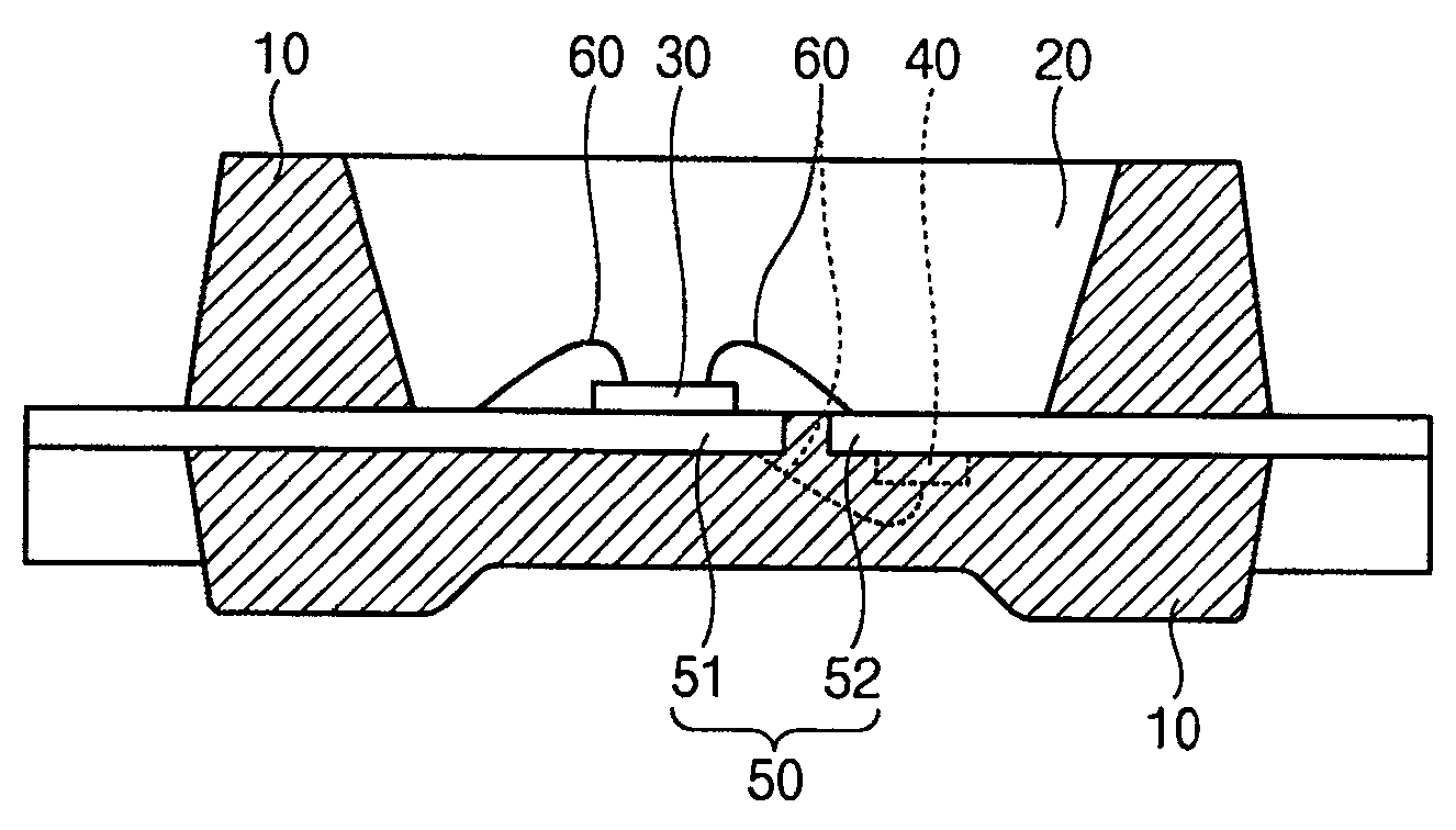
现在,将参照图1和图2详细地描述根据相关技术的具有静电放电损坏防护功能的高亮度LED。Now, a high brightness LED having an electrostatic discharge damage protection function according to the related art will be described in detail with reference to FIGS. 1 and 2 .
图1是示出了根据相关技术的具有静电放电损坏防护功能的高亮度LED的正视图,以及图2是示出了图1所示的具有静电放电损坏防护功能的高亮度LED的平面截面图。1 is a front view showing a high-brightness LED with an electrostatic discharge damage protection function according to the related art, and FIG. 2 is a plan sectional view showing the high-brightness LED with an electrostatic discharge damage protection function shown in FIG. 1 .
如图1和图2所示,根据相关技术的稳压二极管具有如下的平行结构:LED芯片30和由齐纳二极管构成的静电放电损坏防护件40成一直线安装在由一对正极51和负极52构成的引线框的同一表面上,并且LED芯片30和静电放电损坏防护件40通过由金(Au)制成的导线60彼此连接。As shown in FIGS. 1 and 2 , the zener diode according to the related art has a parallel structure as follows:
参考标号10代表由透明或不透明合成树脂制成的封装件,以及参考标号20代表用于保护LED芯片的模塑材料(moldingmaterial)。
作为静电放电损坏防护件40的齐纳二极管也被称作稳压二极管。此外,齐纳二极管作为一种半导体P-N结二极管而制造,使得其运行特性显示在P-N结的击穿区内,并且用于恒压。齐纳二极管通过齐纳恢复(Zener recovery)来获得恒压,以10mA电流在硅的P-N结中运行,并可以根据其类型获得3到12V的稳定电压。Zener diodes as the electrostatic discharge
在根据相关技术的发光二极管中,这种齐纳二极管通过导线与LED芯片并联。因此,尽管由于静电而施加反向电流,齐纳二极管可以防止损坏。In the light emitting diode according to the related art, such a zener diode is connected in parallel with the LED chip through a wire. Therefore, the zener diode prevents damage despite reverse current application due to static electricity.
然而,在根据相关技术的发光二极管中,齐纳二极管和LED芯片并联安装在引线框上。因此,引线框应足够大以保证用于引线接合(wire-bond)的足够区域,从而发光二极管的封装件的尺寸变大,从而难以使发光二极管的封装件小型化。However, in light emitting diodes according to the related art, Zener diodes and LED chips are mounted in parallel on a lead frame. Therefore, the lead frame should be large enough to secure a sufficient area for wire-bond, so that the size of the light emitting diode package becomes large, making it difficult to miniaturize the light emitting diode package.
此外,如果齐纳二极管和LED芯片并联安装在引线框上,则从LED芯片发出的光被齐纳二极管吸收或散射,从而降低了发光二极管的亮度。此外,发光二极管的特性和可靠性恶化,并且发光效率也随之降低。In addition, if the Zener diode and the LED chip are mounted in parallel on the lead frame, the light emitted from the LED chip is absorbed or scattered by the Zener diode, thereby reducing the brightness of the LED. In addition, the characteristics and reliability of the light emitting diodes deteriorate, and the luminous efficiency decreases accordingly.
发明内容 Contents of the invention
本发明的一个优点在于其提供了一种具有静电放电损坏防护功能的高亮度LED,其中,LED芯片和齐纳二极管通过引线框上的导线彼此并联连接,齐纳二极管安装在具有在其上形成的LED芯片的引线框的背面上,使得发光二极管可以免受静电放电损坏,并增强了发光二极管的亮度。An advantage of the present invention is that it provides a high-brightness LED with protection against electrostatic discharge damage, wherein the LED chip and the Zener diode are connected in parallel to each other through wires on the lead frame, and the Zener diode is mounted on a On the back of the lead frame of the LED chip, the light-emitting diode can be protected from electrostatic discharge damage, and the brightness of the light-emitting diode is enhanced.
本发明的总体思想的其它方面和优点部分将在以下的描述中阐明,部分将从描述或总体发明思想的实施中变得显而易见。Additional aspects and advantages of the general inventive concept will be set forth in part in the description which follows, and in part will be obvious from the description or practice of the general inventive concept.
根据本方面的一个方面,具有静电放电损坏防护功能的高亮度LED包括:引线框,包括一对正负极引线;封装件,由合成树脂制成,在其中容纳有引线框的一部分;LED芯片,安装在封装件内部的引线框的上表面上;静电放电损坏防护件,安装在封装件内部的引线框的下表面上,并通过导线与LED芯片并联连接;以及模塑材料,填入封装件中以保护LED芯片。According to an aspect of the present invention, a high-brightness LED having a function of protecting against electrostatic discharge damage includes: a lead frame including a pair of positive and negative electrode leads; a package made of synthetic resin in which a part of the lead frame is housed; an LED chip , installed on the upper surface of the lead frame inside the package; electrostatic discharge damage protection, installed on the lower surface of the lead frame inside the package, and connected in parallel with the LED chip through a wire; and molding material, filled into the package package to protect the LED chip.
根据本发明的另一方面,LED芯片安装在引线框的正极引线的上表面上,以及静电放电损坏防护件安装在引线框的负极引线的下表面上。According to another aspect of the present invention, the LED chip is mounted on the upper surface of the positive lead of the lead frame, and the electrostatic discharge damage guard is mounted on the lower surface of the negative lead of the lead frame.
根据本发明的再一方面,LED芯片安装在引线框的负极引线的上表面上,以及静电放电损坏防护件安装在引线框的正极引线的下表面上。According to still another aspect of the present invention, the LED chip is mounted on the upper surface of the negative lead of the lead frame, and the electrostatic discharge damage guard is mounted on the lower surface of the positive lead of the lead frame.
根据本发明的又一方面,LED芯片安装在引线框的正极引线的上表面上,以及静电放电损坏防护件安装在引线框的正极引线的下表面上。According to still another aspect of the present invention, the LED chip is mounted on the upper surface of the positive lead of the lead frame, and the electrostatic discharge damage guard is mounted on the lower surface of the positive lead of the lead frame.
根据本发明的又一方面,LED芯片安装在引线框的负极引线的上表面上,以及静电放电损坏防护件安装在引线框的负极引线的下表面上。According to still another aspect of the present invention, the LED chip is mounted on the upper surface of the negative electrode lead of the lead frame, and the electrostatic discharge damage guard is mounted on the lower surface of the negative electrode lead of the lead frame.
根据本发明的又一方面,静电放电损坏防护件包括稳压二极管或变阻器,并且稳压二极管包括从齐纳二极管、雪崩二极管、开关二极管、和肖特基二极管所组成的组中选取的二极管。According to yet another aspect of the present invention, the electrostatic discharge damage protection member includes a zener diode or a varistor, and the zener diode includes a diode selected from the group consisting of a Zener diode, an avalanche diode, a switching diode, and a Schottky diode.
附图说明 Description of drawings
本发明的总体思想的这些和/或其它方面及优点将通过以下结合附图对实施例的描述而变得显而易见,并更易于理解。在附图中:These and/or other aspects and advantages of the general inventive concept will become more apparent and easier to understand through the following description of the embodiments in conjunction with the accompanying drawings. In the attached picture:
图1是示出了根据相关技术的具有静电放电损坏防护功能的高亮度LED的正视图;FIG. 1 is a front view showing a high brightness LED having a function of protecting against electrostatic discharge damage according to the related art;
图2是示出了图1所示的具有静电放电损坏防护功能的高亮度LED的平面截面图;FIG. 2 is a plan cross-sectional view showing the high-brightness LED shown in FIG. 1 with an electrostatic discharge damage protection function;
图3是示出了根据本发明第一实施例的具有静电放电损坏防护功能的高亮度LED的正视图;3 is a front view showing a high-brightness LED with an electrostatic discharge damage protection function according to a first embodiment of the present invention;
图4是示出了图3所示的具有静电放电损坏防护功能的高亮度LED的平面截面图;FIG. 4 is a plan sectional view showing the high brightness LED shown in FIG. 3 with an electrostatic discharge damage protection function;
图5是示出了图4所示的具有静电放电损坏防护功能的高亮度LED的反向电流保护电路的示意图;FIG. 5 is a schematic diagram showing a reverse current protection circuit of a high-brightness LED with an electrostatic discharge damage protection function shown in FIG. 4;
图6是示出了根据本发明第二实施例的具有静电放电损坏防护功能的高亮度LED的正视图;6 is a front view showing a high-brightness LED with an electrostatic discharge damage protection function according to a second embodiment of the present invention;
图7是示出了图6所示的具有静电放电损坏防护功能的高亮度LED的平面截面图;7 is a plan sectional view showing the high-brightness LED shown in FIG. 6 with an electrostatic discharge damage protection function;
图8是示出了根据本发明第三实施例的具有静电放电损坏防护功能的高亮度LED的正视图;8 is a front view showing a high-brightness LED with an electrostatic discharge damage protection function according to a third embodiment of the present invention;
图9是示出了图8所示的具有静电放电损坏防护功能的高亮度LED的平面截面图;FIG. 9 is a plan sectional view showing the high brightness LED shown in FIG. 8 with an electrostatic discharge damage protection function;
图10是示出了根据本发明第四实施例的具有静电放电损坏防护功能的高亮度LED的正视图;以及10 is a front view showing a high brightness LED with an electrostatic discharge damage protection function according to a fourth embodiment of the present invention; and
图11是示出了图10所示的具有静电放电损坏防护功能的高亮度LED的平面截面图。FIG. 11 is a plan sectional view showing the high brightness LED shown in FIG. 10 with the electrostatic discharge damage protection function.
具体实施方式 Detailed ways
现在,将详细地参照本发明总体思想的实施例,其实例在附图中示出,其中,相同的参考标号始终表示相同的元件。以下,通过参照附图描述实施例以解释本发明的总体思想。Reference will now be made in detail to embodiments of the present general inventive concept, examples of which are illustrated in the accompanying drawings, wherein like reference numerals refer to like elements throughout. Hereinafter, the embodiments are described in order to explain the present general idea by referring to the figures.
以下,将参照附图详细地描述本发明的优选实施例,使得本领域的普通技术人员可以容易地实施本发明。Hereinafter, preferred embodiments of the present invention will be described in detail with reference to the accompanying drawings so that those skilled in the art can easily implement the present invention.
在附图中,厚度被放大,以清楚地示出不同的层和区域。在整个说明书中,相同的附图标号属于相同或类似的部件。In the drawings, the thicknesses are exaggerated to clearly show different layers and regions. Throughout the specification, the same reference numerals belong to the same or similar parts.
现在,将参照附图描述根据本发明实施例的具有静电放电损坏防护功能的高亮度LED。Now, a high brightness LED having an electrostatic discharge damage protection function according to an embodiment of the present invention will be described with reference to the accompanying drawings.
第一实施例first embodiment
参照图3到图5,详细描述根据本发明第一实施例的具有静电放电防护功能的高亮度LED。Referring to FIG. 3 to FIG. 5 , the high brightness LED with electrostatic discharge protection function according to the first embodiment of the present invention will be described in detail.
图3是示出了根据本发明第一实施例的具有静电放电损坏防护功能的高亮度LED的正视图。图4是示出了图3所示的具有静电放电损坏防护功能的高亮度LED的平面截面图。图5是示出了图3所示的具有静电放电损坏防护功能的高亮度LED的反向电流保护电路的示意图。FIG. 3 is a front view showing a high brightness LED having an electrostatic discharge damage protection function according to a first embodiment of the present invention. FIG. 4 is a plan sectional view showing the high brightness LED shown in FIG. 3 with the electrostatic discharge damage protection function. FIG. 5 is a schematic diagram showing a reverse current protection circuit of the high-brightness LED shown in FIG. 3 with the protection function of electrostatic discharge damage.
如图3到图5所示,根据本发明第一实施例的具有静电放电损坏防护功能的高亮度LED通过引线框50(即,正极引线51和负极引线52)安装在印刷电路板(未示出)或类似物上,该引线框从由合成树脂制成的封装件10突出。3 to 5, according to the first embodiment of the present invention, the high-brightness LED with electrostatic discharge damage protection function is mounted on a printed circuit board (not shown) through a lead frame 50 (ie, a
具有静电放电防护功能的高亮度LED包括典型的LED芯片30,其设置在封装件10内部,以在供电时发光;以及静电放电损坏防护件40,与LED芯片30并联连接,以防止静电的损坏。The high-brightness LED with electrostatic discharge protection function includes a
根据本发明的第一实施例的LED芯片30通过芯片焊接法(diebonding method)由导电性环氧树脂安装在引线框的正极51的上表面上。通过与LED芯片30中相同的方法,静电放电防护件40安装在引线框的负极引线52的下表面上。The
LED芯片30通过导线60电连接到正极引线51和负极引线52,以及静电放电损坏防护件40通过导线60引线接合到正极引线51。The
如图5所示,LED芯片30和静电放电损坏防护件40彼此并联连接。As shown in FIG. 5, the
静电放电损坏防护件40由稳压二极管或变阻器形成。优选地,稳压二极管由从齐纳二极管、雪崩二极管、开关二极管和肖特基二极管所组成的组中选取的二极管形成。在本实施例中,齐纳二极管被用作稳压二极管。The electrostatic
没有被描述的参考标号20代表用于保护LED芯片的模塑材料。
在上述具有静电放电防护功能的高亮度LED中,LED芯片30安装在正极引线51的上表面上,静电放电损坏防护件40安装在负极引线52的下表面上,并且LED芯片30与静电放电损坏防护件40并联连接。因此,尽管由于静电而施加反向电流,电流被静电放电损坏防护件40旁路,从而防止由静电放电损坏所导致的损坏。In the above-mentioned high-brightness LED with electrostatic discharge protection function, the
特别地,具有静电放电损坏防护功能的高亮度LED的静电放电损坏防护件安装在发光LED芯片的背面。换句话说,参照引线框,LED芯片安装在上表面上,并且静电损坏防护件安装在下表面上。因此,位于它们之间的引线框作为交界(barrier),防止由LED芯片发出的光被吸收或散射在静电放电损坏防护件中,从而增强了LED的亮度。In particular, the electrostatic discharge damage protection member of the high brightness LED having the electrostatic discharge damage protection function is mounted on the backside of the light-emitting LED chip. In other words, referring to the lead frame, the LED chip is mounted on the upper surface, and the electrostatic damage guard is mounted on the lower surface. Therefore, the lead frame located between them acts as a barrier, preventing light emitted from the LED chip from being absorbed or scattered in the electrostatic discharge damage protection member, thereby enhancing the brightness of the LED.
第二实施例second embodiment
参照图6和图7,将描述本发明的第二实施例。在此,将省略与第一实施例相同的第二实施例的部件。仅描述不同的部件。Referring to Fig. 6 and Fig. 7, a second embodiment of the present invention will be described. Here, the same components of the second embodiment as those of the first embodiment will be omitted. Only the different components are described.
图6是示出了根据本发明第二实施例的具有静电放电损坏防护功能的高亮度LED的正视图。图7是示出了图6所示的具有静电放电损坏防护功能的高亮度LED的平面截面图。FIG. 6 is a front view showing a high brightness LED having an electrostatic discharge damage protection function according to a second embodiment of the present invention. FIG. 7 is a plan sectional view showing the high brightness LED shown in FIG. 6 with the electrostatic discharge damage protection function.
根据本发明第二实施例的具有静电放电损坏防护功能的高亮度LED具有与根据本发明第一实施例的具有静电放电损坏防护功能的高亮度LED几乎相同的结构。然而,如图6和图7中所示,LED芯片30安装在负极引线52的上表面上,并且静电放电损坏防护件40安装在正极引线51的下表面上,这与第一实施例不同。The high-brightness LED with electrostatic discharge damage protection function according to the second embodiment of the present invention has almost the same structure as the high-brightness LED with electrostatic discharge damage protection function according to the first embodiment of the present invention. However, as shown in FIGS. 6 and 7 , the
与第一实施例相同,LED芯片30和静电放电损坏防护件40彼此并联连接,并同时相对于引线框50一上一下地设置。因此,可以获得与第一实施例相同的效果。Like the first embodiment, the
第三实施例third embodiment
参照图8和图9,将描述本发明的第三实施例。由于第三实施例的大部分部件与第一实施例的部件相同,所以仅描述不同的结构。Referring to Fig. 8 and Fig. 9, a third embodiment of the present invention will be described. Since most of the components of the third embodiment are the same as those of the first embodiment, only the different structures will be described.
图8是示出了根据本发明第三实施例的具有静电放电损坏防护功能的高亮度LED的正视图。图9是示出了图8所示的具有静电放电损坏防护功能的高亮度LED的平面截面图。FIG. 8 is a front view showing a high brightness LED having an electrostatic discharge damage protection function according to a third embodiment of the present invention. FIG. 9 is a plan sectional view showing the high brightness LED shown in FIG. 8 with the electrostatic discharge damage protection function.
如图8和图9所示,即使在根据第三实施例的高亮度LED中,LED芯片30和静电放电损坏防护件40彼此也并联连接,并同时相对于引线框50一上一下地设置。因此,第三实施例可以获得与第一和第二实施例相同的运行和效果。As shown in FIGS. 8 and 9 , even in the high brightness LED according to the third embodiment, the
然而,在根据第三实施例的高亮度LED中,LED芯片30安装在正极引线51的上表面上,并且静电放电损坏防护件40也安装在正极引线51的下表面上,这与第一和第二实施例不同。However, in the high brightness LED according to the third embodiment, the
第四实施例Fourth embodiment
图10和图11示出了根据本发明的第四实施例的具有静电放电损坏防护功能的高亮度LED。如图10和11所示,第四实施例具有与第一到第三实施例相同的结构,其中LED芯片30和静电放电损坏防护件40彼此并联连接,并同时呈现相对于引线框50一上一下地设置。然而,LED芯片30和静电放电损坏防护件40分别安装在负极引线52的上表面和下表面上,这与第一到第三实施例不同。10 and 11 show a high brightness LED with an electrostatic discharge damage protection function according to a fourth embodiment of the present invention. As shown in FIGS. 10 and 11 , the fourth embodiment has the same structure as the first to third embodiments, in which the
即使在第四实施例中,也可以获得与第一和第三实施例相同的运行和效果。Even in the fourth embodiment, the same operations and effects as those of the first and third embodiments can be obtained.
特别地,在如上所述的根据第三和第四实施例的具有静电放电损坏防护功能的高亮度LED中,LED芯片和静电放电损坏防护件安装在相同引线框的上表面和下表面上。因此,与根据第一和第二实施例的具有静电放电损坏防护功能的高亮度LED的尺寸相比,引线框的尺寸可以最小化,这使得LED封装件小型化成为可能。In particular, in the high brightness LED with electrostatic discharge damage protection function according to the third and fourth embodiments as described above, the LED chip and the electrostatic discharge damage protection member are mounted on the upper and lower surfaces of the same lead frame. Therefore, the size of the lead frame can be minimized compared to the size of the high brightness LED with the electrostatic discharge damage protection function according to the first and second embodiments, which makes it possible to miniaturize the LED package.
尽管参照本发明的典型实施例对本发明进行了描述,本领域的技术人员应该明白,在不脱离所附权利要求限定的本发明范围的情况下,可在形式和细节上进行各种修改和改进。Although the present invention has been described with reference to exemplary embodiments thereof, it will be understood to those skilled in the art that various changes and improvements in form and details may be made without departing from the scope of the invention as defined in the appended claims. .
在上述的本发明中,LED芯片和静电放电损坏防护件彼此并联连接,并同时相对于引线框一上一下地安装。因此,尽管由于静电而施加反向电流,该电流被静电放电损坏防护件旁路,从而防止由静电放电所引起的损失。In the present invention described above, the LED chip and the electrostatic discharge damage protection member are connected in parallel with each other while being mounted one above the other with respect to the lead frame. Therefore, although reverse current is applied due to static electricity, the current is bypassed by the electrostatic discharge damage guard, thereby preventing loss caused by electrostatic discharge.
此外,关于引线框,LED芯片安装在上表面上,并且静电放电损坏防护件安装在下表面上。因此,位于它们之间的引线框用作防止从LED芯片发射的光被静电放电损坏防护件吸收或散射,从而增强了LED的相同亮度。Furthermore, regarding the lead frame, the LED chip is mounted on the upper surface, and the electrostatic discharge damage guard is mounted on the lower surface. Therefore, the lead frame located between them serves to prevent the light emitted from the LED chip from being absorbed or scattered by the electrostatic discharge damage guard, thereby enhancing the same luminance of the LED.
此外,LED芯片和静电放电损坏防护件安装在相同引线框的上表面和下表面上。因此,可以使引线框的尺寸最小化,从而使LED封装件小型化。In addition, the LED chip and the electrostatic discharge damage guard are mounted on the upper and lower surfaces of the same lead frame. Therefore, the size of the lead frame can be minimized, thereby miniaturizing the LED package.
尽管示出并描述了总体发明思想的一些实施例,但是应该理解,本领域的技术人员可以在不脱离本发明的总体发明思想的原理和精神、以及所附权利要求及其等同替换范围的情况下,可以对这些实施例进行修改。Although some embodiments of the general inventive concept have been shown and described, it should be understood that those skilled in the art can implement the present invention without departing from the principle and spirit of the general inventive concept of the present invention, as well as the appended claims and their equivalent replacement scopes. Below, these embodiments can be modified.
Claims (10)
Applications Claiming Priority (2)
| Application Number | Priority Date | Filing Date | Title |
|---|---|---|---|
| KR1020050046283A KR100650191B1 (en) | 2005-05-31 | 2005-05-31 | High brightness LEDs with built-in protection against electrostatic discharge shock |
| KR1020050046283 | 2005-05-31 |
Publications (2)
| Publication Number | Publication Date |
|---|---|
| CN1873975A CN1873975A (en) | 2006-12-06 |
| CN100568503C true CN100568503C (en) | 2009-12-09 |
Family
ID=37462245
Family Applications (1)
| Application Number | Title | Priority Date | Filing Date |
|---|---|---|---|
| CNB2006100833010A Active CN100568503C (en) | 2005-05-31 | 2006-05-31 | High Brightness LEDs Protected From ESD Damage |
Country Status (4)
| Country | Link |
|---|---|
| US (1) | US20060267040A1 (en) |
| JP (1) | JP2006339640A (en) |
| KR (1) | KR100650191B1 (en) |
| CN (1) | CN100568503C (en) |
Families Citing this family (50)
| Publication number | Priority date | Publication date | Assignee | Title |
|---|---|---|---|---|
| TWI284433B (en) * | 2006-02-23 | 2007-07-21 | Novalite Optronics Corp | Light emitting diode package and fabricating method thereof |
| KR100820529B1 (en) * | 2006-05-11 | 2008-04-08 | 엘지이노텍 주식회사 | Light emitting device and manufacturing method thereof, surface light emitting device |
| KR101134752B1 (en) * | 2006-07-14 | 2012-04-13 | 엘지이노텍 주식회사 | LED Package |
| DE102007001706A1 (en) | 2007-01-11 | 2008-07-17 | Osram Opto Semiconductors Gmbh | Housing for optoelectronic component and arrangement of an optoelectronic component in a housing |
| US7968900B2 (en) * | 2007-01-19 | 2011-06-28 | Cree, Inc. | High performance LED package |
| JP4903179B2 (en) * | 2007-04-23 | 2012-03-28 | サムソン エルイーディー カンパニーリミテッド. | Light emitting device and manufacturing method thereof |
| US20090026470A1 (en) * | 2007-07-23 | 2009-01-29 | Novalite Optronics Corp. | Super thin side-view light-emitting diode (led) package and fabrication method thereof |
| KR100870950B1 (en) * | 2007-11-19 | 2008-12-01 | 일진반도체 주식회사 | Light emitting diode device and manufacturing method thereof |
| JP5463447B2 (en) * | 2008-01-18 | 2014-04-09 | 三洋電機株式会社 | Light emitting device and lamp provided with the same |
| KR200451054Y1 (en) | 2008-02-01 | 2010-11-22 | 광전자 주식회사 | Lead frame and LED package using same |
| KR200448847Y1 (en) | 2008-03-20 | 2010-05-27 | 주식회사 파워라이텍 | Side Emitting LED Package |
| TWI384649B (en) * | 2008-06-18 | 2013-02-01 | 宏齊科技股份有限公司 | Light emitting diode chip encapsulation structure with embedded electrostatic protection function and its making method |
| KR20100003320A (en) * | 2008-06-24 | 2010-01-08 | 엘지이노텍 주식회사 | Light emitting diode package |
| JP5458910B2 (en) | 2009-02-24 | 2014-04-02 | 日亜化学工業株式会社 | Light emitting device |
| TWI380433B (en) | 2009-02-25 | 2012-12-21 | Everlight Electronics Co Ltd | Light emitting diode package |
| CN101819968B (en) * | 2009-02-27 | 2012-05-23 | 亿光电子工业股份有限公司 | LED Packaging |
| KR101060761B1 (en) | 2009-04-23 | 2011-08-31 | 삼성엘이디 주식회사 | Light emitting diode package |
| RU2525325C2 (en) * | 2010-02-09 | 2014-08-10 | Нития Корпорейшн | Light-emitting device and method to manufacture light-emitting device |
| CN102201395B (en) * | 2010-03-25 | 2013-05-08 | 方伟光 | Multi-layer semiconductor component packaging structure with anti-surge function and manufacturing method thereof |
| KR101298406B1 (en) * | 2010-05-17 | 2013-08-20 | 엘지이노텍 주식회사 | Light Emitting Device |
| JP2012049348A (en) * | 2010-08-27 | 2012-03-08 | Sharp Corp | Light emitting device |
| CN102456826A (en) * | 2010-11-01 | 2012-05-16 | 富士康(昆山)电脑接插件有限公司 | LED (Light-Emitting Diode) lead frame |
| US20120112237A1 (en) * | 2010-11-05 | 2012-05-10 | Shenzhen China Star Optoelectronics Technology Co. Ltd. | Led package structure |
| KR101788723B1 (en) * | 2011-04-28 | 2017-10-20 | 엘지이노텍 주식회사 | Light emitting device package |
| KR101823506B1 (en) | 2011-06-29 | 2018-01-30 | 엘지이노텍 주식회사 | Light emitting device and light unit having thereof |
| KR102042150B1 (en) * | 2012-09-13 | 2019-11-07 | 엘지이노텍 주식회사 | Light emitting device and lighting system |
| DE102013202904A1 (en) | 2013-02-22 | 2014-08-28 | Osram Opto Semiconductors Gmbh | Optoelectronic semiconductor component and method for its production |
| CN106062466B (en) | 2013-11-15 | 2020-01-31 | 瑞尔D斯帕克有限责任公司 | Directional backlight with light emitting element package |
| CN104716246B (en) * | 2013-12-17 | 2017-09-26 | 展晶科技(深圳)有限公司 | Optoelectronic component encapsulation construction and its manufacture method |
| KR102227769B1 (en) | 2014-11-06 | 2021-03-16 | 삼성전자주식회사 | Semiconductor light emitting diode and semiconductor light emitting diode package using the same |
| RU2596062C1 (en) | 2015-03-20 | 2016-08-27 | Автономная Некоммерческая Образовательная Организация Высшего Профессионального Образования "Сколковский Институт Науки И Технологий" | Method for correction of eye image using machine learning and method of machine learning |
| EP3123937B1 (en) * | 2015-07-28 | 2019-08-28 | ams AG | Biometric sensor arrangement and method for generating a biometric signal |
| WO2017091051A1 (en) * | 2015-11-27 | 2017-06-01 | 엘지이노텍 주식회사 | Light-emitting element package and lighting device |
| CN108463787B (en) | 2016-01-05 | 2021-11-30 | 瑞尔D斯帕克有限责任公司 | Gaze correction of multi-perspective images |
| CN105679738B (en) * | 2016-03-24 | 2019-09-06 | 禾邦电子(中国)有限公司 | Chip rectifier element and its production process |
| WO2017200950A1 (en) | 2016-05-19 | 2017-11-23 | Reald Spark, Llc | Wide angle imaging directional backlights |
| EP4124795B1 (en) | 2016-05-23 | 2024-04-10 | RealD Spark, LLC | Wide angle imaging directional backlights |
| KR101790063B1 (en) | 2016-05-26 | 2017-10-25 | 주식회사 시지트로닉스 | Hybrid type module, integrated device and manufacturing method using thereof |
| CN105938866A (en) * | 2016-06-13 | 2016-09-14 | 开发晶照明(厦门)有限公司 | LED bracket and LED package structure |
| US10401638B2 (en) | 2017-01-04 | 2019-09-03 | Reald Spark, Llc | Optical stack for imaging directional backlights |
| US10408992B2 (en) | 2017-04-03 | 2019-09-10 | Reald Spark, Llc | Segmented imaging directional backlights |
| JP6572938B2 (en) * | 2017-05-12 | 2019-09-11 | 日亜化学工業株式会社 | Light emitting device and method for manufacturing light emitting device |
| KR101913508B1 (en) | 2017-07-21 | 2018-10-30 | 여성열 | Linear LED lighting instrument having self indicator |
| CN111183405A (en) | 2017-08-08 | 2020-05-19 | 瑞尔D斯帕克有限责任公司 | Adjusting digital representation of head region |
| WO2019090246A1 (en) | 2017-11-06 | 2019-05-09 | Reald Spark, Llc | Privacy display apparatus |
| CN108092133B (en) * | 2017-12-12 | 2020-01-31 | 湖南艾华集团股份有限公司 | Overvoltage and surge protection device |
| CA3089477A1 (en) | 2018-01-25 | 2019-08-01 | Reald Spark, Llc | Touch screen for privacy display |
| DE102019104325A1 (en) * | 2019-02-20 | 2020-08-20 | OSRAM Opto Semiconductors Gesellschaft mit beschränkter Haftung | Optoelectronic semiconductor component and manufacturing method for optoelectronic semiconductor components |
| KR102042547B1 (en) * | 2019-07-04 | 2019-11-08 | 엘지이노텍 주식회사 | Light emitting device and light unit having thereof |
| CN120076393B (en) * | 2025-04-27 | 2025-07-11 | 苏州达晶微电子有限公司 | TVS device and method for manufacturing the same |
Family Cites Families (14)
| Publication number | Priority date | Publication date | Assignee | Title |
|---|---|---|---|---|
| US3727064A (en) * | 1971-03-17 | 1973-04-10 | Monsanto Co | Opto-isolator devices and method for the fabrication thereof |
| JP2966591B2 (en) * | 1991-08-02 | 1999-10-25 | 三洋電機株式会社 | Optical semiconductor device |
| US5647034A (en) * | 1994-10-03 | 1997-07-08 | Matsushita Electric Works, Ltd. | Operation displaying semiconductor switch |
| JPH10144965A (en) * | 1996-11-11 | 1998-05-29 | Hamamatsu Photonics Kk | Optical semiconductor device and method of manufacturing the same |
| US6054716A (en) * | 1997-01-10 | 2000-04-25 | Rohm Co., Ltd. | Semiconductor light emitting device having a protecting device |
| JPH11103097A (en) * | 1997-07-30 | 1999-04-13 | Rohm Co Ltd | Semiconductor light emitting device |
| US5914501A (en) * | 1998-08-27 | 1999-06-22 | Hewlett-Packard Company | Light emitting diode assembly having integrated electrostatic discharge protection |
| JP2000124506A (en) * | 1998-10-15 | 2000-04-28 | Rohm Co Ltd | Semiconductor light emitting device |
| JP2001036140A (en) * | 1999-07-16 | 2001-02-09 | Stanley Electric Co Ltd | Antistatic surface mount LED |
| JP2002314143A (en) * | 2001-04-09 | 2002-10-25 | Toshiba Corp | Light emitting device |
| KR20030033590A (en) * | 2001-10-24 | 2003-05-01 | (주)옵토니카 | Light emitting device for comprising voltage regulator device and method thereof |
| TW563264B (en) * | 2002-10-11 | 2003-11-21 | Highlink Technology Corp | Base of optoelectronic device |
| JP3789428B2 (en) | 2002-12-06 | 2006-06-21 | 星和電機株式会社 | Light emitting device |
| CN100587560C (en) * | 2003-04-01 | 2010-02-03 | 夏普株式会社 | Light-emitting device module, light-emitting device, backside light irradiation device, and display device |
-
2005
- 2005-05-31 KR KR1020050046283A patent/KR100650191B1/en not_active Expired - Fee Related
-
2006
- 2006-05-29 JP JP2006147999A patent/JP2006339640A/en active Pending
- 2006-05-31 CN CNB2006100833010A patent/CN100568503C/en active Active
- 2006-05-31 US US11/442,957 patent/US20060267040A1/en not_active Abandoned
Also Published As
| Publication number | Publication date |
|---|---|
| US20060267040A1 (en) | 2006-11-30 |
| CN1873975A (en) | 2006-12-06 |
| KR100650191B1 (en) | 2006-11-27 |
| JP2006339640A (en) | 2006-12-14 |
Similar Documents
| Publication | Publication Date | Title |
|---|---|---|
| CN100568503C (en) | High Brightness LEDs Protected From ESD Damage | |
| CN103210510B (en) | Optoelectronic Semiconductor Devices | |
| US20070246729A1 (en) | High efficiency LED package | |
| CN101562178B (en) | Semiconductor light-emitting device | |
| KR100769720B1 (en) | High brightness LEDs with built-in protection against electrostatic discharge shock | |
| JP2011525702A (en) | Light emitting device package | |
| KR100604408B1 (en) | Light emitting diode package | |
| EP1207563A2 (en) | Direct bonding of flip-chip light-emitting diode and flip-chip ESD protection chip to electrodes in a package | |
| KR101309069B1 (en) | Led package including a constant current diode chip | |
| JP2010182803A (en) | Light-emitting apparatus | |
| TW200929595A (en) | Packaging structure of electro-optic device with ESD protection | |
| KR101762597B1 (en) | Substrate for semiconductor light emitting device | |
| JP3787220B2 (en) | Chip light emitting device | |
| KR102131853B1 (en) | Light emitting diode array | |
| KR100748241B1 (en) | High brightness LEDs with built-in protection against electrostatic discharge shock and manufacturing method | |
| KR101719641B1 (en) | Light emitting device | |
| KR100591688B1 (en) | Leadframe and Side Light Emitting Diode Package Using the Same | |
| KR100831712B1 (en) | LED chip and LED package including the same | |
| KR100674857B1 (en) | LED package with reinforced electrostatic discharge (ESD) and its manufacturing method | |
| KR101974088B1 (en) | Light emitting diode device | |
| KR101109688B1 (en) | Light-emitting diode union capacitor for preventing electrostatic discharge | |
| KR20160128516A (en) | Semiconductor light emitting device package | |
| KR101946910B1 (en) | Light emitting device, lightr emitting module and lighting system | |
| KR200342558Y1 (en) | Side-type light emitting diode package | |
| KR20090064717A (en) | Light emitting diode package |
Legal Events
| Date | Code | Title | Description |
|---|---|---|---|
| C06 | Publication | ||
| PB01 | Publication | ||
| C10 | Entry into substantive examination | ||
| SE01 | Entry into force of request for substantive examination | ||
| C14 | Grant of patent or utility model | ||
| GR01 | Patent grant | ||
| ASS | Succession or assignment of patent right |
Owner name: SAMSUNG LED CO., LTD. Free format text: FORMER OWNER: SAMSUNG ELECTRO-MECHANICS CO., LTD. Effective date: 20100826 |
|
| C41 | Transfer of patent application or patent right or utility model | ||
| TR01 | Transfer of patent right |
Effective date of registration: 20100826 Address after: Gyeonggi Do, South Korea Patentee after: Samsung LED Co., Ltd. Address before: Gyeonggi Do, South Korea Patentee before: Samsung Electro-Mechanics Co., Ltd. |
|
| ASS | Succession or assignment of patent right |
Owner name: SAMSUNG ELECTRONICS CO., LTD. Free format text: FORMER OWNER: SAMSUNG LED CO., LTD. Effective date: 20121211 |
|
| C41 | Transfer of patent application or patent right or utility model | ||
| TR01 | Transfer of patent right |
Effective date of registration: 20121211 Address after: Gyeonggi Do, South Korea Patentee after: Samsung Electronics Co., Ltd. Address before: Gyeonggi Do, South Korea Patentee before: Samsung LED Co., Ltd. |