CN100524707C - 用于印刷电路组件的底部填充膜 - Google Patents
用于印刷电路组件的底部填充膜 Download PDFInfo
- Publication number
- CN100524707C CN100524707C CNB2004800028872A CN200480002887A CN100524707C CN 100524707 C CN100524707 C CN 100524707C CN B2004800028872 A CNB2004800028872 A CN B2004800028872A CN 200480002887 A CN200480002887 A CN 200480002887A CN 100524707 C CN100524707 C CN 100524707C
- Authority
- CN
- China
- Prior art keywords
- printed circuit
- pcb
- circuit board
- encapsulation
- bottom filling
- Prior art date
- Legal status (The legal status is an assumption and is not a legal conclusion. Google has not performed a legal analysis and makes no representation as to the accuracy of the status listed.)
- Expired - Fee Related
Links
- 230000000712 assembly Effects 0.000 title 1
- 238000000429 assembly Methods 0.000 title 1
- 239000000853 adhesive Substances 0.000 claims abstract description 60
- 230000001070 adhesive effect Effects 0.000 claims abstract description 60
- 238000005538 encapsulation Methods 0.000 claims description 108
- 238000003466 welding Methods 0.000 claims description 45
- 238000000576 coating method Methods 0.000 claims description 6
- 239000011248 coating agent Substances 0.000 claims description 5
- 229920001169 thermoplastic Polymers 0.000 claims description 3
- 239000004416 thermosoftening plastic Substances 0.000 claims description 3
- 239000000975 dye Substances 0.000 claims description 2
- 239000011256 inorganic filler Substances 0.000 claims description 2
- 229910003475 inorganic filler Inorganic materials 0.000 claims description 2
- 239000000654 additive Substances 0.000 claims 1
- 239000000049 pigment Substances 0.000 claims 1
- 229910000679 solder Inorganic materials 0.000 abstract description 7
- 238000000034 method Methods 0.000 description 11
- 239000000945 filler Substances 0.000 description 8
- 230000035939 shock Effects 0.000 description 6
- 238000006116 polymerization reaction Methods 0.000 description 5
- 239000002313 adhesive film Substances 0.000 description 4
- 238000004519 manufacturing process Methods 0.000 description 4
- 239000011230 binding agent Substances 0.000 description 3
- 230000015572 biosynthetic process Effects 0.000 description 3
- 238000006243 chemical reaction Methods 0.000 description 3
- 239000000463 material Substances 0.000 description 3
- 230000008569 process Effects 0.000 description 3
- IYZWUWBAFUBNCH-UHFFFAOYSA-N 2,6-dichlorobiphenyl Chemical compound ClC1=CC=CC(Cl)=C1C1=CC=CC=C1 IYZWUWBAFUBNCH-UHFFFAOYSA-N 0.000 description 2
- GWEVSGVZZGPLCZ-UHFFFAOYSA-N Titan oxide Chemical compound O=[Ti]=O GWEVSGVZZGPLCZ-UHFFFAOYSA-N 0.000 description 2
- 238000013459 approach Methods 0.000 description 2
- 230000008901 benefit Effects 0.000 description 2
- 230000008859 change Effects 0.000 description 2
- 238000009792 diffusion process Methods 0.000 description 2
- 230000004907 flux Effects 0.000 description 2
- 230000004048 modification Effects 0.000 description 2
- 238000012986 modification Methods 0.000 description 2
- 230000003647 oxidation Effects 0.000 description 2
- 238000007254 oxidation reaction Methods 0.000 description 2
- 238000012545 processing Methods 0.000 description 2
- OKTJSMMVPCPJKN-UHFFFAOYSA-N Carbon Chemical compound [C] OKTJSMMVPCPJKN-UHFFFAOYSA-N 0.000 description 1
- 239000004642 Polyimide Substances 0.000 description 1
- 208000034189 Sclerosis Diseases 0.000 description 1
- ATJFFYVFTNAWJD-UHFFFAOYSA-N Tin Chemical compound [Sn] ATJFFYVFTNAWJD-UHFFFAOYSA-N 0.000 description 1
- 229910052799 carbon Inorganic materials 0.000 description 1
- 239000003795 chemical substances by application Substances 0.000 description 1
- 238000001816 cooling Methods 0.000 description 1
- 238000000354 decomposition reaction Methods 0.000 description 1
- 238000013461 design Methods 0.000 description 1
- 229920001971 elastomer Polymers 0.000 description 1
- 230000005670 electromagnetic radiation Effects 0.000 description 1
- 239000003822 epoxy resin Substances 0.000 description 1
- 230000002349 favourable effect Effects 0.000 description 1
- 239000000835 fiber Substances 0.000 description 1
- 239000011152 fibreglass Substances 0.000 description 1
- 239000011521 glass Substances 0.000 description 1
- PCHJSUWPFVWCPO-UHFFFAOYSA-N gold Chemical compound [Au] PCHJSUWPFVWCPO-UHFFFAOYSA-N 0.000 description 1
- 239000010931 gold Substances 0.000 description 1
- 229910052737 gold Inorganic materials 0.000 description 1
- 230000006872 improvement Effects 0.000 description 1
- 239000007788 liquid Substances 0.000 description 1
- 239000007791 liquid phase Substances 0.000 description 1
- 238000012423 maintenance Methods 0.000 description 1
- 230000007246 mechanism Effects 0.000 description 1
- 230000005499 meniscus Effects 0.000 description 1
- 229910052751 metal Inorganic materials 0.000 description 1
- 239000002184 metal Substances 0.000 description 1
- 238000012856 packing Methods 0.000 description 1
- 229920000647 polyepoxide Polymers 0.000 description 1
- 229920000728 polyester Polymers 0.000 description 1
- 229920001721 polyimide Polymers 0.000 description 1
- 229920000642 polymer Polymers 0.000 description 1
- 239000004814 polyurethane Substances 0.000 description 1
- 229920002635 polyurethane Polymers 0.000 description 1
- 239000010453 quartz Substances 0.000 description 1
- 230000002787 reinforcement Effects 0.000 description 1
- 230000000717 retained effect Effects 0.000 description 1
- VYPSYNLAJGMNEJ-UHFFFAOYSA-N silicon dioxide Inorganic materials O=[Si]=O VYPSYNLAJGMNEJ-UHFFFAOYSA-N 0.000 description 1
- 238000005476 soldering Methods 0.000 description 1
- 239000007787 solid Substances 0.000 description 1
- 239000003351 stiffener Substances 0.000 description 1
- 239000000758 substrate Substances 0.000 description 1
- 229920001187 thermosetting polymer Polymers 0.000 description 1
- 239000004634 thermosetting polymer Substances 0.000 description 1
- 239000004408 titanium dioxide Substances 0.000 description 1
Images


Classifications
-
- H—ELECTRICITY
- H05—ELECTRIC TECHNIQUES NOT OTHERWISE PROVIDED FOR
- H05K—PRINTED CIRCUITS; CASINGS OR CONSTRUCTIONAL DETAILS OF ELECTRIC APPARATUS; MANUFACTURE OF ASSEMBLAGES OF ELECTRICAL COMPONENTS
- H05K3/00—Apparatus or processes for manufacturing printed circuits
- H05K3/30—Assembling printed circuits with electric components, e.g. with resistor
- H05K3/303—Surface mounted components, e.g. affixing before soldering, aligning means, spacing means
- H05K3/305—Affixing by adhesive
-
- H—ELECTRICITY
- H05—ELECTRIC TECHNIQUES NOT OTHERWISE PROVIDED FOR
- H05K—PRINTED CIRCUITS; CASINGS OR CONSTRUCTIONAL DETAILS OF ELECTRIC APPARATUS; MANUFACTURE OF ASSEMBLAGES OF ELECTRICAL COMPONENTS
- H05K3/00—Apparatus or processes for manufacturing printed circuits
- H05K3/22—Secondary treatment of printed circuits
- H05K3/28—Applying non-metallic protective coatings
-
- H—ELECTRICITY
- H05—ELECTRIC TECHNIQUES NOT OTHERWISE PROVIDED FOR
- H05K—PRINTED CIRCUITS; CASINGS OR CONSTRUCTIONAL DETAILS OF ELECTRIC APPARATUS; MANUFACTURE OF ASSEMBLAGES OF ELECTRICAL COMPONENTS
- H05K7/00—Constructional details common to different types of electric apparatus
- H05K7/02—Arrangements of circuit components or wiring on supporting structure
- H05K7/10—Plug-in assemblages of components, e.g. IC sockets
- H05K7/1053—Plug-in assemblages of components, e.g. IC sockets having interior leads
-
- H—ELECTRICITY
- H01—ELECTRIC ELEMENTS
- H01L—SEMICONDUCTOR DEVICES NOT COVERED BY CLASS H10
- H01L2224/00—Indexing scheme for arrangements for connecting or disconnecting semiconductor or solid-state bodies and methods related thereto as covered by H01L24/00
- H01L2224/01—Means for bonding being attached to, or being formed on, the surface to be connected, e.g. chip-to-package, die-attach, "first-level" interconnects; Manufacturing methods related thereto
- H01L2224/26—Layer connectors, e.g. plate connectors, solder or adhesive layers; Manufacturing methods related thereto
- H01L2224/28—Structure, shape, material or disposition of the layer connectors prior to the connecting process
- H01L2224/29—Structure, shape, material or disposition of the layer connectors prior to the connecting process of an individual layer connector
- H01L2224/29001—Core members of the layer connector
- H01L2224/2901—Shape
- H01L2224/29012—Shape in top view
- H01L2224/29015—Shape in top view comprising protrusions or indentations
-
- H—ELECTRICITY
- H01—ELECTRIC ELEMENTS
- H01L—SEMICONDUCTOR DEVICES NOT COVERED BY CLASS H10
- H01L2224/00—Indexing scheme for arrangements for connecting or disconnecting semiconductor or solid-state bodies and methods related thereto as covered by H01L24/00
- H01L2224/01—Means for bonding being attached to, or being formed on, the surface to be connected, e.g. chip-to-package, die-attach, "first-level" interconnects; Manufacturing methods related thereto
- H01L2224/26—Layer connectors, e.g. plate connectors, solder or adhesive layers; Manufacturing methods related thereto
- H01L2224/28—Structure, shape, material or disposition of the layer connectors prior to the connecting process
- H01L2224/30—Structure, shape, material or disposition of the layer connectors prior to the connecting process of a plurality of layer connectors
- H01L2224/301—Disposition
- H01L2224/3012—Layout
- H01L2224/3015—Mirror array, i.e. array having only a reflection symmetry, i.e. bilateral symmetry
- H01L2224/30154—Mirror array, i.e. array having only a reflection symmetry, i.e. bilateral symmetry covering only portions of the surface to be connected
- H01L2224/30155—Covering only the peripheral area of the surface to be connected, i.e. peripheral arrangements
-
- H—ELECTRICITY
- H01—ELECTRIC ELEMENTS
- H01L—SEMICONDUCTOR DEVICES NOT COVERED BY CLASS H10
- H01L2224/00—Indexing scheme for arrangements for connecting or disconnecting semiconductor or solid-state bodies and methods related thereto as covered by H01L24/00
- H01L2224/01—Means for bonding being attached to, or being formed on, the surface to be connected, e.g. chip-to-package, die-attach, "first-level" interconnects; Manufacturing methods related thereto
- H01L2224/26—Layer connectors, e.g. plate connectors, solder or adhesive layers; Manufacturing methods related thereto
- H01L2224/31—Structure, shape, material or disposition of the layer connectors after the connecting process
- H01L2224/32—Structure, shape, material or disposition of the layer connectors after the connecting process of an individual layer connector
- H01L2224/3205—Shape
- H01L2224/32057—Shape in side view
- H01L2224/32058—Shape in side view being non uniform along the layer connector
-
- H—ELECTRICITY
- H01—ELECTRIC ELEMENTS
- H01L—SEMICONDUCTOR DEVICES NOT COVERED BY CLASS H10
- H01L2224/00—Indexing scheme for arrangements for connecting or disconnecting semiconductor or solid-state bodies and methods related thereto as covered by H01L24/00
- H01L2224/73—Means for bonding being of different types provided for in two or more of groups H01L2224/10, H01L2224/18, H01L2224/26, H01L2224/34, H01L2224/42, H01L2224/50, H01L2224/63, H01L2224/71
- H01L2224/731—Location prior to the connecting process
- H01L2224/73101—Location prior to the connecting process on the same surface
- H01L2224/73103—Bump and layer connectors
-
- H—ELECTRICITY
- H01—ELECTRIC ELEMENTS
- H01L—SEMICONDUCTOR DEVICES NOT COVERED BY CLASS H10
- H01L2224/00—Indexing scheme for arrangements for connecting or disconnecting semiconductor or solid-state bodies and methods related thereto as covered by H01L24/00
- H01L2224/73—Means for bonding being of different types provided for in two or more of groups H01L2224/10, H01L2224/18, H01L2224/26, H01L2224/34, H01L2224/42, H01L2224/50, H01L2224/63, H01L2224/71
- H01L2224/732—Location after the connecting process
- H01L2224/73201—Location after the connecting process on the same surface
- H01L2224/73203—Bump and layer connectors
-
- H—ELECTRICITY
- H05—ELECTRIC TECHNIQUES NOT OTHERWISE PROVIDED FOR
- H05K—PRINTED CIRCUITS; CASINGS OR CONSTRUCTIONAL DETAILS OF ELECTRIC APPARATUS; MANUFACTURE OF ASSEMBLAGES OF ELECTRICAL COMPONENTS
- H05K2201/00—Indexing scheme relating to printed circuits covered by H05K1/00
- H05K2201/01—Dielectrics
- H05K2201/0104—Properties and characteristics in general
- H05K2201/0129—Thermoplastic polymer, e.g. auto-adhesive layer; Shaping of thermoplastic polymer
-
- H—ELECTRICITY
- H05—ELECTRIC TECHNIQUES NOT OTHERWISE PROVIDED FOR
- H05K—PRINTED CIRCUITS; CASINGS OR CONSTRUCTIONAL DETAILS OF ELECTRIC APPARATUS; MANUFACTURE OF ASSEMBLAGES OF ELECTRICAL COMPONENTS
- H05K2201/00—Indexing scheme relating to printed circuits covered by H05K1/00
- H05K2201/09—Shape and layout
- H05K2201/09818—Shape or layout details not covered by a single group of H05K2201/09009 - H05K2201/09809
- H05K2201/09909—Special local insulating pattern, e.g. as dam around component
-
- H—ELECTRICITY
- H05—ELECTRIC TECHNIQUES NOT OTHERWISE PROVIDED FOR
- H05K—PRINTED CIRCUITS; CASINGS OR CONSTRUCTIONAL DETAILS OF ELECTRIC APPARATUS; MANUFACTURE OF ASSEMBLAGES OF ELECTRICAL COMPONENTS
- H05K2201/00—Indexing scheme relating to printed circuits covered by H05K1/00
- H05K2201/10—Details of components or other objects attached to or integrated in a printed circuit board
- H05K2201/10613—Details of electrical connections of non-printed components, e.g. special leads
- H05K2201/10621—Components characterised by their electrical contacts
- H05K2201/10734—Ball grid array [BGA]; Bump grid array
-
- H—ELECTRICITY
- H05—ELECTRIC TECHNIQUES NOT OTHERWISE PROVIDED FOR
- H05K—PRINTED CIRCUITS; CASINGS OR CONSTRUCTIONAL DETAILS OF ELECTRIC APPARATUS; MANUFACTURE OF ASSEMBLAGES OF ELECTRICAL COMPONENTS
- H05K2203/00—Indexing scheme relating to apparatus or processes for manufacturing printed circuits covered by H05K3/00
- H05K2203/01—Tools for processing; Objects used during processing
- H05K2203/0191—Using tape or non-metallic foil in a process, e.g. during filling of a hole with conductive paste
-
- H—ELECTRICITY
- H05—ELECTRIC TECHNIQUES NOT OTHERWISE PROVIDED FOR
- H05K—PRINTED CIRCUITS; CASINGS OR CONSTRUCTIONAL DETAILS OF ELECTRIC APPARATUS; MANUFACTURE OF ASSEMBLAGES OF ELECTRICAL COMPONENTS
- H05K3/00—Apparatus or processes for manufacturing printed circuits
- H05K3/30—Assembling printed circuits with electric components, e.g. with resistor
- H05K3/32—Assembling printed circuits with electric components, e.g. with resistor electrically connecting electric components or wires to printed circuits
- H05K3/34—Assembling printed circuits with electric components, e.g. with resistor electrically connecting electric components or wires to printed circuits by soldering
- H05K3/341—Surface mounted components
- H05K3/3431—Leadless components
- H05K3/3436—Leadless components having an array of bottom contacts, e.g. pad grid array or ball grid array components
-
- Y—GENERAL TAGGING OF NEW TECHNOLOGICAL DEVELOPMENTS; GENERAL TAGGING OF CROSS-SECTIONAL TECHNOLOGIES SPANNING OVER SEVERAL SECTIONS OF THE IPC; TECHNICAL SUBJECTS COVERED BY FORMER USPC CROSS-REFERENCE ART COLLECTIONS [XRACs] AND DIGESTS
- Y02—TECHNOLOGIES OR APPLICATIONS FOR MITIGATION OR ADAPTATION AGAINST CLIMATE CHANGE
- Y02P—CLIMATE CHANGE MITIGATION TECHNOLOGIES IN THE PRODUCTION OR PROCESSING OF GOODS
- Y02P70/00—Climate change mitigation technologies in the production process for final industrial or consumer products
- Y02P70/50—Manufacturing or production processes characterised by the final manufactured product
Landscapes
- Engineering & Computer Science (AREA)
- Microelectronics & Electronic Packaging (AREA)
- Manufacturing & Machinery (AREA)
- Wire Bonding (AREA)
- Electric Connection Of Electric Components To Printed Circuits (AREA)
- Non-Metallic Protective Coatings For Printed Circuits (AREA)
Abstract
自支持底部填充膜(18)粘附性地使表面安装集成电路封装(14)键合到印刷电路板(10)上。印刷电路板在表面上具有导电迹线(12)和露出的导电焊盘(13)。膜粘合剂关键设置在靠近导电焊盘的印刷电路板上,然后把表面安装印刷电路板封装放置在板上,使得封装上的导电焊盘(16)对准板上的导电焊盘。当使封装焊接到板上时,膜粘合剂软化,并且膜最终用作底部填充以增强焊接点的机械完整性。
Description
美国政府已批准本发明和权利在限定的情况内,以要求专利权人在由NIST批准的许可号No.70NANB8H4007的条款所提供的合理条件下许可其他人使用。
技术领域
本发明通常涉及印刷电路组件。更具体地,本发明涉及底部填充粘合剂的利用以使表面安装集成电路封装键合到印刷电路板上。
背景技术
借助于表面安装焊接点,使例如倒装芯片(FC)或球栅阵列(BGA)封装的集成电路(IC)封装直接附着到印刷电路板(PCB)上。现今,在从计算机到移动电话的电子产品中广泛使用这种技术,以产生非常有效、高密度的产品。
然而,当这些封装被固定在印刷电路板上时,通过许多机构、例如焊接点或电路迹线的裂缝、或焊接焊盘可以从PCB分层,转移到焊接点上的机械应力能使互连系统中断。这些机械应力可以产生于许多来源,例如封装和PCB之间的热失配,但最普遍地是当电子产品跌落时由机械震动所引起的。一段时间已知对于这种问题的一种常见解决方法。具体地,液相聚合材料、所谓的“底部填充”在封装焊接到PCB上之后在封装下面流动。一旦底部填充完全填充了存在于倒装芯片底部和基板之间的小间隙时,通过聚合使材料变硬。变硬的、聚合的底部填充使IC封装和PCB固定在一起,使得几乎不存在任何细微的移动。通过控制将另外形成在芯片和PCB之间的接合处的额外应力,可以制造可靠的组件。
当底部填充的传统利用已解决了PCB上的机械震动问题时,产生了一系列严重的制造问题。首先,必须用特殊的设备使预先聚合的液体底部填充受到二级处理。一般地,底部填充涂敷到已组装的封装的一个、两个或三个边缘,并且使得在已固定的封装下面自始至终流动。一旦材料流动到相反边缘,并且从芯片下面已排出全部空气,那么可以使额外的底部填充扩散到那些外部边缘以形成嵌条(fillet)。嵌条增加了可靠性并即使其需要额外的制造时间也是通常优选的。接着,在烘炉中烘焙组件以聚合并硬化底部填充,再次增加了处理的时间。该烘焙处理正常占10至30分钟,虽然其可能会占用几个小时,并且附加的设备和其维护显著增加了制造成本。从而,当底部填充的利用有助于减轻了机械震动问题并提供了商业解决方案,但电子器件制造工业寻求具有更低附加成本的更有效的制造方法。
最近,已发展了改进和流水线化的底部填充工艺。一种方法包括在IC封装组配到板上之前扩散底部填充到IC封装上。在焊接之前预先扩散的底部填充应含有助熔剂或具有促进焊接点形成的特性。由于电路上的焊盘常常氧化以及由于IC封装上的锡/铅焊接凸起通常氧化,所以必须设计助熔剂和底部填充来减少这些氧化物涂布并促进焊接点形成。当简化IC封装组件工艺时,该方法仍将需要额外的步骤。不管由IC封装底部填充技术所提供的各种优点,也仍需要涂敷底部填充的更简单方法。还存在用于减少了由底部填充涂敷所需的大量工艺步骤的工艺方法的需要。
发明内容
根据本发明的一个方面,提供了一种印刷电路组件,包括:印刷电路板,在其主表面上具有多条导电迹线;表面安装集成电路封装,在其主表面上具有导电焊盘的阵列,所述封装安装在所述印刷电路板上,使得导电焊盘的阵列的至少一部分接触导电迹线的相应部分;底部填充粘合剂,设置在所述封装和所述印刷电路板之间,使得底部填充粘附性地使所述封装键合到所述印刷电路板上;以及其中,在使所述封装附着到所述板上之前,涂敷所述底部填充粘合剂作为游离薄膜到所述印刷电路板主表面上,其中所述底部填充粘合剂不完全在封装周边的周围延伸。
根据本发明的另一个方面,提供了一种印刷电路组件,包括:印刷电路板,在其主表面上具有多条导电迹线;表面安装集成电路封装,在其主表面上具有导电焊盘的阵列,所述封装安装在所述印刷电路板上,使得导电焊盘的阵列的至少一部分接触导电迹线的相应部分;底部填充粘合剂,设置在所述封装和所述印刷电路板之间,使得底部填充粘附性地使所述封装键合到所述印刷电路板上;以及其中,在使所述封装附着到所述板上之前,涂敷所述底部填充粘合剂作为游离薄膜到所述印刷电路板主表面上;其中游离薄膜是“L”形状的,并且放置在所述阵列的角处。
根据本发明的再一个方面,提供了一种印刷电路组件,包括:印刷电路板,在其主表面上具有多条导电迹线;表面安装集成电路封装,在其主表面上具有导电焊盘的阵列,所述封装安装在所述印刷电路板上,使得导电焊盘的阵列的至少一部分接触导电迹线的相应部分;底部填充粘合剂,设置在所述封装和所述印刷电路板之间,使得底部填充粘附性地使所述封装键合到所述印刷电路板上;以及其中,在使所述封装附着到所述板上之前,涂敷所述底部填充粘合剂作为游离薄膜到所述印刷电路板主表面上;其中游离薄膜是张开的丝网栅格。
根据本发明,还提供了一种印刷电路组件,包括:印刷电路板,在其主表面上具有多条导电迹线;表面安装集成电路封装,在其主表面上具有导电焊盘的阵列,所述封装安装在所述印刷电路板上,使得导电焊盘的阵列的至少一部分接触导电迹线的相应部分;底部填充粘合剂,沿所述封装主表面的周边的至少一部分设置在所述封装和所述印刷电路板之间,以粘附性地使所述封装键合到所述印刷电路板上;以及其中,在使所述封装附着到所述板上之前,涂敷所述底部填充粘合剂作为游离薄膜到所述印刷电路板主表面上,而在涂敷之后,软化所述底部填充粘合剂以流动并使所述封装键合到所述印刷电路板上,其中所述底部填充粘合剂不完全在封装周边的周围延伸。
根据本发明,进一步提供了一种印刷电路组件,包括:印刷电路板,在其主表面上具有多条导电迹线;表面安装集成电路封装,在其主表面上具有导电焊盘的阵列,所述封装安装在所述印刷电路板上,使得导电焊盘的阵列的至少一部分接触导电迹线的相应部分;底部填充粘合剂,沿所述封装主表面的周边的至少一部分设置在所述封装和所述印刷电路板之间,以粘附性地使所述封装键合到所述印刷电路板上;以及其中,在使所述封装附着到所述板上之前,涂敷所述底部填充粘合剂作为游离薄膜到所述印刷电路板主表面上,而在涂敷之后,软化所述底部填充粘合剂以流动并使所述封装键合到所述印刷电路板上,其中游离薄膜是“L”形状的,并且被放置在所述阵列的角处。
根据本发明,还提供了一种印刷电路组件,包括:印刷电路板,在其主表面上具有多条导电焊盘;表面安装集成电路封装,在其主表面上具有焊接凸起的阵列,所述凸起焊接到导电焊盘上;底部填充粘合剂,沿所述封装主表面的周边的一部分设置在所述封装和所述印刷电路板之间,使得底部填充粘附性地使所述封装键合到所述印刷电路板上;以及其中,在焊接所述凸起到所述导电焊盘之前,涂敷所述底部填充粘合剂作为游离薄膜到所述印刷电路板主表面上,其中所述底部填充粘合剂不完全在封装周边的周围延伸。
附图说明
用权利要求中的特性来阐明认为是新颖的本发明的特征。然而,参考介绍了本发明确定的示范性实施例的本发明的下列详细说明,可以与其目的和优点一起最好地理解发明本身及其构造和操作方法。在以下说明中,在附图的几个视图中,相同的参考数字用来描述相同、相似或相应的元件,其中:
图1是根据本发明安装在印刷电路板上的球栅阵列封装的等角视图。
图2是根据本发明安装在印刷电路板上的球栅阵列封装的分解侧视图。
图3和4是根据本发明各种实施例安装在印刷电路板上的球栅阵列封装的局部侧视图。
图5是具有附着到其上的底部填充膜的印刷电路板的局部平面图,用来描绘根据本发明一个实施例的膜的布置。
图6是具有附着到其上的底部填充膜的印刷电路板的局部平面图,用来描绘根据本发明另一个实施例的膜的布置。
具体实施方式
尽管本发明能容许许多不同形式的实施例,在附图中示出并在此处详细介绍具体的实施例,应明白本公开可看作为本发明的原理的一个例子并不意图将本发明限制为所示和所述的具体实施例。在下列说明中,在附图的几个视图中相同的参考数字用于描述相同、相似或相应的元件。
自支持的底部填充膜附着地使表面安装集成电路封装键合到印刷电路板上。印刷电路板在表面上具有导电迹线和露出的导电焊盘。膜粘合剂关键定位在靠近导电焊盘的印刷电路板上,并随后把凸起的表面安装集成电路封装放置在印刷电路板上,使得在封装上的导电焊盘对准板上的导电焊盘。当把封装焊接在板上时软化膜粘合剂,并且膜最终用作底部填充以增加焊点的机械完整性。
现在参考图1和2,按传统方式,设计用于表面安装元件的印刷电路板10在至少一个主表面或侧面11上具有导电迹线12。PCB 10还具有位于侧面上并连接至少一些导电迹线12的多个导电焊盘13,其一般按一定的图案排列、例如阵列,并适合于接收集成电路封装14。通常露出导电焊盘13,以便成为IC封装14和PCB上的迹线12之间的电连接。IC封装、例如球栅阵列、倒装芯片封装、或其它类型的区域阵列表面安装封装通常在封装的底面上具有接触或端子16的阵列,其按本领域普通技术人员所周知的传统方式连接集成电路。这些接触16一般凸起有焊接球以使IC封装回流焊接到PCB上的相应导电焊盘13上。自支持膜粘合剂18放置在导电焊盘13附近而不与其接触的PCB上。粘合剂膜18用作IC封装14和PCB 10之间的底部填充并在使封装焊接到PCB上之后用于加固组件。现在参考图5,在一个实施例中,按字母“L”的形状剪切粘合剂膜58并关键放置在导电焊盘的阵列的四个角的每个角处。仔细定位粘合剂膜,使得其靠近独立的导电焊盘,而不接触焊盘,以便不妨碍IC封装对PCB的焊接。与现有技术不一样的是在粘附到PCB之后分布底部填充,另外与现有技术不一样的是在IC封装上预先分布底部填充,我们的发明实现了在IC封装放置在PCB的时间之前,放置到PCB上的粘合剂的自支持膜。因为底部填充粘合剂是按自支持膜的形式,所以其例如可以预先封装成带和卷轴形式,以便正如任何其它的电子元件一样通过安置工具或自动仪器来很容易地操作。实际上,恰好在放置IC封装之前,通过至少一个安置工具使膜放置到PCB上,并保留在适当的位置处,直到IC封装被存放到该位置上。当IC封装放置在PCB上时,膜和封装保留在适当的位置。在回流焊接步骤期间,IC封装上的焊接凸起熔化并被焊接到PCB导电焊盘13上,同时底部填充粘合剂膜18软化并流动以形成围绕IC封装的外部边缘的嵌条(fillet),如图1中所示。当然,软化和流动的程度取决于选择用于底部填充膜的特性。例如,在焊接步骤期间,热塑性粘合剂将软化并流动,并随后在冷却到室温时变硬。热固性粘合剂、例如环氧树脂、聚脂、聚氨基甲酸酯和聚酰亚胺将很少会经历(experiencelittle)或不软化,并通常比热塑性塑料流动差,但在凝固成刚硬的固体之前仍产生一小的嵌条。在任一情况下,在冷却时,粘合剂变硬以在适当地位置处牢固地锁住IC封装,并在电子产品的寿命周期可能出现的随后机械震动期间防止细微的移动。
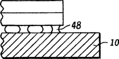
现在参考图3,流动的底部填充膜粘合剂将形成类似于该所示的嵌条38,具有接触IC封装底侧的一部分嵌条和向上延伸到封装的外侧边缘的一部分以形成一弯月面形。在该优选实施例中,底部填充延伸在封装边缘以外,并且我们发现这提供了耐机械震动的优良抵抗性。图4示出了完全在IC封装下面的底部填充膜粘合剂48,形成一凹入的嵌条。实际上,我们已发现该构造提供了改善的抗震动性,但不会达到在封装边缘外侧的优选嵌条的情况下所发现的程度。如上所述和图5中所描绘的,粘合剂膜58的优选形状是“L”形状,在阵列的每个角上的单个“L”形状的膜锁住了IC封装的角但却不会接触PCB上的独立的焊接焊盘13。在“L”形状的膜之间的间隙提供了沿封装周长的每条边的中间的开口,以使在焊接操作中所产生的挥发性气体从封装的下面逸出。这些开口通过增加IC封装下面的导热还更快速地焊接。图6中示出了本发明的一可替换实施例,其中自支持底部填充粘合剂膜68是以丝网或栅格图案的形式,包围PCB阵列上的独立的焊接焊盘13或焊盘的组。
自支持粘合剂底部填充膜18可以是纯聚合物,或其可以填充有填充物以改变粘合剂的物理特性。例如,许多的无机填充物、例如石英、二氧化钛、碳素纤维、微球等对于本领域那些技术人员来说是公知的并能随同有机染料一起被很容易地添加到膜里。这是有利的,因为其减少了膜的固有的柔软性,使得更容易在自动工厂里操作。还可以利用堆叠膜,例如,具有作为在两层粘合剂膜之间的中心核心的纵向堆叠的加劲构件(stiffener)。可以把例如金属箔、玻璃纤维垫、纸片或一层完全凝固的热固性聚合物的加劲构件堆叠到粘合剂膜上。
总之,在不意图限制本发明的范围的情况下,在印刷电路板上提供用于表面安装IC封装的底部填充的新颖方法,利用了在放置IC封装之前放置在PCB上的粘合剂的自支持膜。然后在回流焊接期间凝固或软化膜以使IC封装键合到PCB上,由此防止来自机械震动的应力被集中在焊接点处。本领域那些技术人员应认识到,按照基于在玻璃加强型印刷电路板上焊接凸起球栅阵列的利用的示范性实施例,已介绍了本发明。然而,由于对于本领域技术人员考虑到此处的讲解将会产生其它变化,所以本发明不应如此受到限制。例如,尽管本发明主要针对焊接凸起和回流的IC封装,人们还可以利用具有附着方法的其它非焊接类型的本发明,例如导电油墨、导电橡胶、镀金焊盘等,系统的这些类型包括在权利要求中。可选择地,人们可以利用不软化或流动、却根据接触简单地锁定IC封装在适当位置的力敏型粘合剂,或利用通过电磁辐射软化或凝固的粘合剂。
当结合具体实施例来描述本发明时,很明显,根据上述说明,许多转换、修改、变更和变化对于本领域那些普通技术人员来说将变得显而易见。因此,意图使本发明包含落入权利要求范围内的所有这种转换、修改和变换。
Claims (10)
1.一种印刷电路组件,包括:
印刷电路板,在其主表面上具有多条导电迹线;
表面安装集成电路封装,在其主表面上具有导电焊盘的阵列,所述封装安装在所述印刷电路板上,使得导电焊盘的阵列的至少一部分接触导电迹线的相应部分;
底部填充粘合剂,设置在所述封装和所述印刷电路板之间,使得底部填充粘合剂使所述封装键合到所述印刷电路板上;以及
其中,在使所述封装附着到所述板上之前,涂敷所述底部填充粘合剂作为游离薄膜到所述印刷电路板主表面上,其中所述底部填充粘合剂不完全在封装周边的周围延伸。
2.一种印刷电路组件,包括:
印刷电路板,在其主表面上具有多条导电迹线;
表面安装集成电路封装,在其主表面上具有导电焊盘的阵列,所述封装安装在所述印刷电路板上,使得导电焊盘的阵列的至少一部分接触导电迹线的相应部分;
底部填充粘合剂,设置在所述封装和所述印刷电路板之间,使得底部填充粘合剂使所述封装键合到所述印刷电路板上;以及
其中,在使所述封装附着到所述板上之前,涂敷所述底部填充粘合剂作为游离薄膜到所述印刷电路板主表面上;
其中游离薄膜是“L”形状的,并且放置在所述阵列的角处。
3.一种印刷电路组件,包括:
印刷电路板,在其主表面上具有多条导电迹线;
表面安装集成电路封装,在其主表面上具有导电焊盘的阵列,所述封装安装在所述印刷电路板上,使得导电焊盘的阵列的至少一部分接触导电迹线的相应部分;
底部填充粘合剂,设置在所述封装和所述印刷电路板之间,使得底部填充粘合剂使所述封装键合到所述印刷电路板上;以及
其中,在使所述封装附着到所述板上之前,涂敷所述底部填充粘合剂作为游离薄膜到所述印刷电路板主表面上;
其中游离薄膜是张开的丝网栅格。
4.一种印刷电路组件,包括:
印刷电路板,在其主表面上具有多条导电迹线;
表面安装集成电路封装,在其主表面上具有导电焊盘的阵列,所述封装安装在所述印刷电路板上,使得导电焊盘的阵列的至少一部分接触导电迹线的相应部分;
底部填充粘合剂,沿所述封装主表面的周边的至少一部分设置在所述封装和所述印刷电路板之间,以粘附性地使所述封装键合到所述印刷电路板上;以及
其中,在使所述封装附着到所述板上之前,涂敷所述底部填充粘合剂作为游离薄膜到所述印刷电路板主表面上,而在涂敷之后,软化所述底部填充粘合剂以流动并使所述封装键合到所述印刷电路板上;
其中游离薄膜是“L”形状的,并且被放置在所述阵列的角处。
5.一种印刷电路组件,包括:
印刷电路板,在其主表面上具有多条导电迹线;
表面安装集成电路封装,在其主表面上具有导电焊盘的阵列,所述封装安装在所述印刷电路板上,使得导电焊盘的阵列的至少一部分接触导电迹线的相应部分;
底部填充粘合剂,沿所述封装主表面的周边的至少一部分设置在所述封装和所述印刷电路板之间,以粘附性地使所述封装键合到所述印刷电路板上;以及
其中,在使所述封装附着到所述板上之前,涂敷所述底部填充粘合剂作为游离薄膜到所述印刷电路板主表面上,而在涂敷之后,软化所述底部填充粘合剂以流动并使所述封装键合到所述印刷电路板上,其中所述底部填充粘合剂不完全在封装周边的周围延伸。
6.如权利要求5中所述的印刷电路组件,其中一部分底部填充粘合剂延伸到封装边缘以外。
7.如权利要求5中所述的印刷电路组件,其中底部填充粘合剂含有选自由无机填充物、染料、颜料和固化层构成的组中的一种或多种添加剂。
8.如权利要求5中所述的印刷电路组件,其中底部填充粘合剂是热固性粘合剂。
9.如权利要求5中所述的印刷电路组件,其中底部填充粘合剂是热塑性粘合剂。
10.一种印刷电路组件,包括:
印刷电路板,在其主表面上具有多条导电焊盘;
表面安装集成电路封装,在其主表面上具有焊接凸起的阵列,所述凸起焊接到导电焊盘上;
底部填充粘合剂,沿所述封装主表面的周边的一部分设置在所述封装和所述印刷电路板之间,使得底部填充粘合剂使所述封装键合到所述印刷电路板上;以及
其中,在焊接所述凸起到所述导电焊盘之前,涂敷所述底部填充粘合剂作为游离薄膜到所述印刷电路板主表面上,其中所述底部填充粘合剂不完全在封装周边的周围延伸。
Applications Claiming Priority (2)
| Application Number | Priority Date | Filing Date | Title |
|---|---|---|---|
| US10/356,419 | 2003-01-31 | ||
| US10/356,419 US7265994B2 (en) | 2003-01-31 | 2003-01-31 | Underfill film for printed wiring assemblies |
Publications (2)
| Publication Number | Publication Date |
|---|---|
| CN1742369A CN1742369A (zh) | 2006-03-01 |
| CN100524707C true CN100524707C (zh) | 2009-08-05 |
Family
ID=32770803
Family Applications (1)
| Application Number | Title | Priority Date | Filing Date |
|---|---|---|---|
| CNB2004800028872A Expired - Fee Related CN100524707C (zh) | 2003-01-31 | 2004-01-30 | 用于印刷电路组件的底部填充膜 |
Country Status (5)
| Country | Link |
|---|---|
| US (1) | US7265994B2 (zh) |
| JP (1) | JP4724652B2 (zh) |
| KR (1) | KR101054239B1 (zh) |
| CN (1) | CN100524707C (zh) |
| WO (1) | WO2004071140A2 (zh) |
Families Citing this family (16)
| Publication number | Priority date | Publication date | Assignee | Title |
|---|---|---|---|---|
| KR20020053326A (ko) * | 2000-12-27 | 2002-07-05 | 이일희 | 폐옥을 이용한 건축자재 제조방법 |
| KR100475540B1 (ko) * | 2002-05-27 | 2005-03-10 | 양원모 | 건축물 마감재의 제조 방법 |
| US6978540B2 (en) | 2003-05-23 | 2005-12-27 | National Starch And Chemical Investment Holding Corporation | Method for pre-applied thermoplastic reinforcement of electronic components |
| US7004375B2 (en) | 2003-05-23 | 2006-02-28 | National Starch And Chemical Investment Holding Corporation | Pre-applied fluxing underfill composition having pressure sensitive adhesive properties |
| US7889959B2 (en) * | 2008-02-07 | 2011-02-15 | Lockheed Martin Corporation | Composite material for cable floatation jacket |
| JP2010103336A (ja) * | 2008-10-24 | 2010-05-06 | Fujitsu Ltd | 基板ユニット、情報処理装置及び基板ユニットの製造方法 |
| US20110115099A1 (en) * | 2009-05-14 | 2011-05-19 | Vertical Circuits, Inc. | Flip-chip underfill |
| KR20110024291A (ko) * | 2009-09-01 | 2011-03-09 | 삼성전기주식회사 | 회로 기판, 반도체 패키지 및 회로 기판의 제조 방법 |
| US20110067910A1 (en) * | 2009-09-18 | 2011-03-24 | International Business Machines Corporation | Component securing system and associated method |
| US10429929B2 (en) | 2010-09-24 | 2019-10-01 | Blackberry Limited | Piezoelectric actuator apparatus and methods |
| FR2994768B1 (fr) | 2012-08-21 | 2016-02-05 | Commissariat Energie Atomique | Hybridation face contre face de deux composants microelectroniques a l'aide d'un recuit uv |
| US20150064851A1 (en) * | 2013-09-03 | 2015-03-05 | Rohm And Haas Electronic Materials Llc | Pre-applied underfill |
| KR20170064594A (ko) | 2015-12-01 | 2017-06-12 | 삼성디스플레이 주식회사 | 전자 소자의 실장 방법 및 이에 사용되는 언더 필 필름 |
| CN107025481B (zh) * | 2016-02-02 | 2021-08-20 | 上海伯乐电子有限公司 | 柔性印制电路板及应用其的智能卡模块和智能卡 |
| KR20180014903A (ko) | 2016-08-01 | 2018-02-12 | 삼성디스플레이 주식회사 | 전자 소자, 이의 실장 방법 및 이를 포함하는 표시 장치의 제조 방법 |
| CN113438826B (zh) * | 2021-06-29 | 2022-10-28 | 荣成歌尔微电子有限公司 | 底填胶封装方法及设备 |
Family Cites Families (20)
| Publication number | Priority date | Publication date | Assignee | Title |
|---|---|---|---|---|
| US5859470A (en) * | 1992-11-12 | 1999-01-12 | International Business Machines Corporation | Interconnection of a carrier substrate and a semiconductor device |
| GB9502178D0 (en) * | 1995-02-03 | 1995-03-22 | Plessey Semiconductors Ltd | MCM-D Assemblies |
| US5836715A (en) * | 1995-11-19 | 1998-11-17 | Clark-Schwebel, Inc. | Structural reinforcement member and method of utilizing the same to reinforce a product |
| JPH1084014A (ja) * | 1996-07-19 | 1998-03-31 | Shinko Electric Ind Co Ltd | 半導体装置の製造方法 |
| US5796169A (en) * | 1996-11-19 | 1998-08-18 | International Business Machines Corporation | Structurally reinforced ball grid array semiconductor package and systems |
| JPH10163386A (ja) * | 1996-12-03 | 1998-06-19 | Toshiba Corp | 半導体装置、半導体パッケージおよび実装回路装置 |
| WO1998028788A1 (en) * | 1996-12-24 | 1998-07-02 | Nitto Denko Corporation | Manufacture of semiconductor device |
| JP3604248B2 (ja) * | 1997-02-25 | 2004-12-22 | 沖電気工業株式会社 | 半導体装置の製造方法 |
| US6040630A (en) * | 1998-04-13 | 2000-03-21 | Harris Corporation | Integrated circuit package for flip chip with alignment preform feature and method of forming same |
| US6139705A (en) * | 1998-05-06 | 2000-10-31 | Eltech Systems Corporation | Lead electrode |
| TW457603B (en) * | 1998-12-02 | 2001-10-01 | Seiko Epson Corp | Anisotropic conductor film, method of packaging semiconductor device, and semiconductor chip |
| US6657313B1 (en) * | 1999-01-19 | 2003-12-02 | International Business Machines Corporation | Dielectric interposer for chip to substrate soldering |
| US6291899B1 (en) * | 1999-02-16 | 2001-09-18 | Micron Technology, Inc. | Method and apparatus for reducing BGA warpage caused by encapsulation |
| JP3447620B2 (ja) * | 1999-07-05 | 2003-09-16 | Necエレクトロニクス株式会社 | フリップチップ実装型半導体装置の製造方法 |
| JP3654116B2 (ja) * | 2000-03-10 | 2005-06-02 | セイコーエプソン株式会社 | 半導体装置及びその製造方法、回路基板並びに電子機器 |
| US6570259B2 (en) * | 2001-03-22 | 2003-05-27 | International Business Machines Corporation | Apparatus to reduce thermal fatigue stress on flip chip solder connections |
| US20020162679A1 (en) * | 2001-05-04 | 2002-11-07 | Nael Hannan | Package level pre-applied underfills for thermo-mechanical reliability enhancements of electronic assemblies |
| JP4417596B2 (ja) * | 2001-09-19 | 2010-02-17 | 富士通株式会社 | 電子部品の実装方法 |
| US6696748B1 (en) * | 2002-08-23 | 2004-02-24 | Micron Technology, Inc. | Stress balanced semiconductor packages, method of fabrication and modified mold segment |
| US6877964B2 (en) * | 2002-11-06 | 2005-04-12 | The United States Of America As Represented By The Secretary Of The Air Force | Multifunction microfluidics device |
-
2003
- 2003-01-31 US US10/356,419 patent/US7265994B2/en not_active Expired - Lifetime
-
2004
- 2004-01-30 KR KR1020057014068A patent/KR101054239B1/ko active IP Right Grant
- 2004-01-30 WO PCT/US2004/002615 patent/WO2004071140A2/en active Application Filing
- 2004-01-30 JP JP2006503178A patent/JP4724652B2/ja not_active Expired - Lifetime
- 2004-01-30 CN CNB2004800028872A patent/CN100524707C/zh not_active Expired - Fee Related
Also Published As
| Publication number | Publication date |
|---|---|
| WO2004071140A3 (en) | 2005-04-28 |
| JP4724652B2 (ja) | 2011-07-13 |
| JP2006517348A (ja) | 2006-07-20 |
| US20040150967A1 (en) | 2004-08-05 |
| KR101054239B1 (ko) | 2011-08-08 |
| KR20050092456A (ko) | 2005-09-21 |
| CN1742369A (zh) | 2006-03-01 |
| US7265994B2 (en) | 2007-09-04 |
| WO2004071140A2 (en) | 2004-08-19 |
Similar Documents
| Publication | Publication Date | Title |
|---|---|---|
| CN100524707C (zh) | 用于印刷电路组件的底部填充膜 | |
| US5133495A (en) | Method of bonding flexible circuit to circuitized substrate to provide electrical connection therebetween | |
| US8035035B2 (en) | Multi-layer wiring board and method of manufacturing the same | |
| KR101053226B1 (ko) | 그의 상하면에 반도체 구성체를 갖는 반도체장치 및 그 제조방법 | |
| US5435732A (en) | Flexible circuit member | |
| US5203075A (en) | Method of bonding flexible circuit to cicuitized substrate to provide electrical connection therebetween using different solders | |
| CN100444374C (zh) | 印刷电路板和包括印刷电路板的电子设备 | |
| CN101601127B (zh) | 导电性凸起及其制造方法以及电子部件安装结构体 | |
| US6400033B1 (en) | Reinforcing solder connections of electronic devices | |
| US20070127224A1 (en) | Electronic circuit device and method of manufacturing the same | |
| US20080303145A1 (en) | Printed Circuit Board, Printed Circuit Board Manufacturing Method and Electronic Device | |
| JPH0567869A (ja) | 電装部品接合方法並びにモジユール及び多層基板 | |
| KR20080066607A (ko) | 다층 배선 기판의 제조 방법 | |
| US6483191B2 (en) | Semiconductor device having reinforced coupling between solder balls and substrate | |
| JP4051570B2 (ja) | 半導体装置の製造方法 | |
| US20030020145A1 (en) | Semiconductor device having reinforced coupling between solder balls and substrate | |
| US7019403B2 (en) | Adhesive film and tacking pads for printed wiring assemblies | |
| KR101199614B1 (ko) | 프린트 배선판 유닛, 전자기기, 및 프린트 배선판 유닛의 제작 방법 | |
| CN102209434B (zh) | 印制电路板以及印制电路板的制造方法 | |
| US11705400B2 (en) | Semiconductor package | |
| US20240136322A1 (en) | Semiconductor package and manufacturing method therefor | |
| US20230276575A1 (en) | Embedded printed circuit board | |
| US20230199967A1 (en) | Embedded printed circuit board | |
| JP2007266640A (ja) | 半導体装置及びその製造方法、回路基板並びに電子機器 | |
| CN101321433B (zh) | 组件固着印刷电路板上的结构及其固着方法 |
Legal Events
| Date | Code | Title | Description |
|---|---|---|---|
| C06 | Publication | ||
| PB01 | Publication | ||
| C10 | Entry into substantive examination | ||
| SE01 | Entry into force of request for substantive examination | ||
| C14 | Grant of patent or utility model | ||
| GR01 | Patent grant | ||
| CP01 | Change in the name or title of a patent holder |
Address after: Texas in the United States Patentee after: NXP USA, Inc. Address before: Texas in the United States Patentee before: FREESCALE SEMICONDUCTOR, Inc. |
|
| CP01 | Change in the name or title of a patent holder | ||
| CF01 | Termination of patent right due to non-payment of annual fee |
Granted publication date: 20090805 |
|
| CF01 | Termination of patent right due to non-payment of annual fee |