CN100465356C - High surface quality GaN wafer and method of fabricating same - Google Patents
High surface quality GaN wafer and method of fabricating same Download PDFInfo
- Publication number
- CN100465356C CN100465356C CNB028114140A CN02811414A CN100465356C CN 100465356 C CN100465356 C CN 100465356C CN B028114140 A CNB028114140 A CN B028114140A CN 02811414 A CN02811414 A CN 02811414A CN 100465356 C CN100465356 C CN 100465356C
- Authority
- CN
- China
- Prior art keywords
- wafer
- mechanical polishing
- slurry
- abrasive
- opto
- Prior art date
- Legal status (The legal status is an assumption and is not a legal conclusion. Google has not performed a legal analysis and makes no representation as to the accuracy of the status listed.)
- Expired - Lifetime
Links
Images


Classifications
-
- H—ELECTRICITY
- H01—ELECTRIC ELEMENTS
- H01L—SEMICONDUCTOR DEVICES NOT COVERED BY CLASS H10
- H01L21/00—Processes or apparatus adapted for the manufacture or treatment of semiconductor or solid state devices or of parts thereof
- H01L21/02—Manufacture or treatment of semiconductor devices or of parts thereof
- H01L21/04—Manufacture or treatment of semiconductor devices or of parts thereof the devices having at least one potential-jump barrier or surface barrier, e.g. PN junction, depletion layer or carrier concentration layer
- H01L21/18—Manufacture or treatment of semiconductor devices or of parts thereof the devices having at least one potential-jump barrier or surface barrier, e.g. PN junction, depletion layer or carrier concentration layer the devices having semiconductor bodies comprising elements of Group IV of the Periodic System or AIIIBV compounds with or without impurities, e.g. doping materials
- H01L21/20—Deposition of semiconductor materials on a substrate, e.g. epitaxial growth solid phase epitaxy
-
- C—CHEMISTRY; METALLURGY
- C30—CRYSTAL GROWTH
- C30B—SINGLE-CRYSTAL GROWTH; UNIDIRECTIONAL SOLIDIFICATION OF EUTECTIC MATERIAL OR UNIDIRECTIONAL DEMIXING OF EUTECTOID MATERIAL; REFINING BY ZONE-MELTING OF MATERIAL; PRODUCTION OF A HOMOGENEOUS POLYCRYSTALLINE MATERIAL WITH DEFINED STRUCTURE; SINGLE CRYSTALS OR HOMOGENEOUS POLYCRYSTALLINE MATERIAL WITH DEFINED STRUCTURE; AFTER-TREATMENT OF SINGLE CRYSTALS OR A HOMOGENEOUS POLYCRYSTALLINE MATERIAL WITH DEFINED STRUCTURE; APPARATUS THEREFOR
- C30B33/00—After-treatment of single crystals or homogeneous polycrystalline material with defined structure
-
- C—CHEMISTRY; METALLURGY
- C09—DYES; PAINTS; POLISHES; NATURAL RESINS; ADHESIVES; COMPOSITIONS NOT OTHERWISE PROVIDED FOR; APPLICATIONS OF MATERIALS NOT OTHERWISE PROVIDED FOR
- C09G—POLISHING COMPOSITIONS; SKI WAXES
- C09G1/00—Polishing compositions
- C09G1/02—Polishing compositions containing abrasives or grinding agents
-
- C—CHEMISTRY; METALLURGY
- C09—DYES; PAINTS; POLISHES; NATURAL RESINS; ADHESIVES; COMPOSITIONS NOT OTHERWISE PROVIDED FOR; APPLICATIONS OF MATERIALS NOT OTHERWISE PROVIDED FOR
- C09K—MATERIALS FOR MISCELLANEOUS APPLICATIONS, NOT PROVIDED FOR ELSEWHERE
- C09K3/00—Materials not provided for elsewhere
- C09K3/14—Anti-slip materials; Abrasives
- C09K3/1409—Abrasive particles per se
-
- C—CHEMISTRY; METALLURGY
- C09—DYES; PAINTS; POLISHES; NATURAL RESINS; ADHESIVES; COMPOSITIONS NOT OTHERWISE PROVIDED FOR; APPLICATIONS OF MATERIALS NOT OTHERWISE PROVIDED FOR
- C09K—MATERIALS FOR MISCELLANEOUS APPLICATIONS, NOT PROVIDED FOR ELSEWHERE
- C09K3/00—Materials not provided for elsewhere
- C09K3/14—Anti-slip materials; Abrasives
- C09K3/1454—Abrasive powders, suspensions and pastes for polishing
- C09K3/1463—Aqueous liquid suspensions
-
- C—CHEMISTRY; METALLURGY
- C30—CRYSTAL GROWTH
- C30B—SINGLE-CRYSTAL GROWTH; UNIDIRECTIONAL SOLIDIFICATION OF EUTECTIC MATERIAL OR UNIDIRECTIONAL DEMIXING OF EUTECTOID MATERIAL; REFINING BY ZONE-MELTING OF MATERIAL; PRODUCTION OF A HOMOGENEOUS POLYCRYSTALLINE MATERIAL WITH DEFINED STRUCTURE; SINGLE CRYSTALS OR HOMOGENEOUS POLYCRYSTALLINE MATERIAL WITH DEFINED STRUCTURE; AFTER-TREATMENT OF SINGLE CRYSTALS OR A HOMOGENEOUS POLYCRYSTALLINE MATERIAL WITH DEFINED STRUCTURE; APPARATUS THEREFOR
- C30B25/00—Single-crystal growth by chemical reaction of reactive gases, e.g. chemical vapour-deposition growth
- C30B25/02—Epitaxial-layer growth
-
- C—CHEMISTRY; METALLURGY
- C30—CRYSTAL GROWTH
- C30B—SINGLE-CRYSTAL GROWTH; UNIDIRECTIONAL SOLIDIFICATION OF EUTECTIC MATERIAL OR UNIDIRECTIONAL DEMIXING OF EUTECTOID MATERIAL; REFINING BY ZONE-MELTING OF MATERIAL; PRODUCTION OF A HOMOGENEOUS POLYCRYSTALLINE MATERIAL WITH DEFINED STRUCTURE; SINGLE CRYSTALS OR HOMOGENEOUS POLYCRYSTALLINE MATERIAL WITH DEFINED STRUCTURE; AFTER-TREATMENT OF SINGLE CRYSTALS OR A HOMOGENEOUS POLYCRYSTALLINE MATERIAL WITH DEFINED STRUCTURE; APPARATUS THEREFOR
- C30B29/00—Single crystals or homogeneous polycrystalline material with defined structure characterised by the material or by their shape
- C30B29/10—Inorganic compounds or compositions
- C30B29/40—AIIIBV compounds wherein A is B, Al, Ga, In or Tl and B is N, P, As, Sb or Bi
- C30B29/403—AIII-nitrides
-
- H—ELECTRICITY
- H01—ELECTRIC ELEMENTS
- H01L—SEMICONDUCTOR DEVICES NOT COVERED BY CLASS H10
- H01L21/00—Processes or apparatus adapted for the manufacture or treatment of semiconductor or solid state devices or of parts thereof
- H01L21/02—Manufacture or treatment of semiconductor devices or of parts thereof
- H01L21/02002—Preparing wafers
- H01L21/02005—Preparing bulk and homogeneous wafers
- H01L21/02008—Multistep processes
- H01L21/0201—Specific process step
- H01L21/02019—Chemical etching
-
- H—ELECTRICITY
- H01—ELECTRIC ELEMENTS
- H01L—SEMICONDUCTOR DEVICES NOT COVERED BY CLASS H10
- H01L21/00—Processes or apparatus adapted for the manufacture or treatment of semiconductor or solid state devices or of parts thereof
- H01L21/02—Manufacture or treatment of semiconductor devices or of parts thereof
- H01L21/02002—Preparing wafers
- H01L21/02005—Preparing bulk and homogeneous wafers
- H01L21/02008—Multistep processes
- H01L21/0201—Specific process step
- H01L21/02024—Mirror polishing
-
- H—ELECTRICITY
- H01—ELECTRIC ELEMENTS
- H01L—SEMICONDUCTOR DEVICES NOT COVERED BY CLASS H10
- H01L21/00—Processes or apparatus adapted for the manufacture or treatment of semiconductor or solid state devices or of parts thereof
- H01L21/02—Manufacture or treatment of semiconductor devices or of parts thereof
- H01L21/04—Manufacture or treatment of semiconductor devices or of parts thereof the devices having at least one potential-jump barrier or surface barrier, e.g. PN junction, depletion layer or carrier concentration layer
- H01L21/18—Manufacture or treatment of semiconductor devices or of parts thereof the devices having at least one potential-jump barrier or surface barrier, e.g. PN junction, depletion layer or carrier concentration layer the devices having semiconductor bodies comprising elements of Group IV of the Periodic System or AIIIBV compounds with or without impurities, e.g. doping materials
- H01L21/30—Treatment of semiconductor bodies using processes or apparatus not provided for in groups H01L21/20 - H01L21/26
- H01L21/302—Treatment of semiconductor bodies using processes or apparatus not provided for in groups H01L21/20 - H01L21/26 to change their surface-physical characteristics or shape, e.g. etching, polishing, cutting
- H01L21/306—Chemical or electrical treatment, e.g. electrolytic etching
- H01L21/30604—Chemical etching
- H01L21/30612—Etching of AIIIBV compounds
- H01L21/30617—Anisotropic liquid etching
-
- H—ELECTRICITY
- H01—ELECTRIC ELEMENTS
- H01L—SEMICONDUCTOR DEVICES NOT COVERED BY CLASS H10
- H01L33/00—Semiconductor devices with at least one potential-jump barrier or surface barrier specially adapted for light emission; Processes or apparatus specially adapted for the manufacture or treatment thereof or of parts thereof; Details thereof
- H01L33/005—Processes
- H01L33/0062—Processes for devices with an active region comprising only III-V compounds
- H01L33/0075—Processes for devices with an active region comprising only III-V compounds comprising nitride compounds
-
- Y—GENERAL TAGGING OF NEW TECHNOLOGICAL DEVELOPMENTS; GENERAL TAGGING OF CROSS-SECTIONAL TECHNOLOGIES SPANNING OVER SEVERAL SECTIONS OF THE IPC; TECHNICAL SUBJECTS COVERED BY FORMER USPC CROSS-REFERENCE ART COLLECTIONS [XRACs] AND DIGESTS
- Y10—TECHNICAL SUBJECTS COVERED BY FORMER USPC
- Y10T—TECHNICAL SUBJECTS COVERED BY FORMER US CLASSIFICATION
- Y10T428/00—Stock material or miscellaneous articles
- Y10T428/21—Circular sheet or circular blank
Abstract
A high quality wafer comprising AlxGayInzN, wherein 0<y<=1 and x+y+z=1, characterized by a root mean square surface roughness of less than 1 nm in a 10 x 10[micro]m<2> arera at its Gaside. Such wafer is chemically mechanically polished (CMP) at its Ga-side, using a CMP slurry comprising abrasive particles, such as silica or alumina, and an acid or a base. The process of fabricating such high quality AlxGayInzN wafer may include steps of lapping, mechanical polishing, and reducing internal stress of said wafer by thermal annealing or chemical etching for further enhancement of its surface quality. The CMP process is usefuffy employed to highlight crystal defects on the Ga-side of the AlxGayInzN wafer.
Description
Background of invention
I. invention field
The present invention relates to Al
xGa
yIn
zN (wherein 0<y≤1 and x+y+z=1) semiconductor wafer, this wafer has excellent surface quality in its Ga-side, the invention still further relates to the production method of this wafer.
II. the description of related art
With general formula Al
xGa
yIn
zN, the GaN that represents of 0<y≤1 and x+y+z=1 and relevant wherein like GaN III-V crystal of nitride film, be useful material in various application, described application examples temperature electronics, drive electronic is in this way learned and photoelectronics (for example photodiode (LEDs) and blue streak laser diode (LDs)).(LED ' s) and laser apparatus are start-up technique, and making in the structure of magnetic-optical memory and CDROM and panchromatic active display has higher storage density to send out the blue streak diode.Send out the blue streak diode and can replace in present highway and the railway signal employed incandescent light etc., can save the actual cost and the energy.
At present, because high quality Al
xGa
yIn
zThe non-practicality of N substrate, Al
xGa
yIn
zThat the N film grows in usually is non--natural substrate such as sapphire or silicon carbide on.But, these foreign substrate and epitaxially grown Al thereon
xGa
yIn
zThe coefficient of expansion between the N crystallization is different with the lattice coefficient, at the Al of described growth
xGa
yIn
zCause very big thermal stresses and internal stress in the N crystallization.Described thermal stresses and internal stress can cause Al
xGa
yIn
zN crystalline fine fisssure, distortion and other defective, thus make these Al
xGa
yIn
zThe N crystallization is broken easily.Growth on unmatched foreign substrate lattice causes highdensity lattice imperfection, causes bad device performance.
For Al in growth
xGa
yIn
zReduce deleterious thermal stresses and high defective density in the N crystallization, be desirable to provide high-quality no supporting al
xGa
yIn
zThe N wafer is as the film growth substrates, to replace above-mentioned foreign substrate.
U.S.P 5,679,152, and denomination of invention is " Method for Making a Single CrystalGa
*N Article " and U.S.P 5,679,153, denomination of invention is for " Bulk Single CrystalGallium Nitride and Method of Making Same " discloses hydride evaporation phase epitaxy growth method (HVPE) to prepare unsupported Al
xGa
yIn
zN crystallization, this crystallization can be favourable as the crystalline growth substrate, be used to make Al
xGa
yIn
zN crystallization isoepitaxial growth thereon.
Because the Al of subsequent growth
xGa
yIn
zN crystalline quality is directly connected to Al
xGa
yIn
zThe quality in the zone on substrate surface that the N crystallization is grown thereon and approaching surface, therefore, it is very important that the level and smooth initial substrate surface of height without any damage under surface and the surface is provided.
But, after mechanical polishing, Al
xGa
yIn
zN crystalline surface quality is generally all very poor, has the damage down of substantial surface and surface, and the polishing scratch.Therefore, additional wafer process technology must be arranged, so that can further improve no supporting al
xGa
yIn
zN crystalline quality so just goes for high quality epitaxial growth and fabricate devices thereon.
Crystalline Al
xGa
yIn
zN generally exists with chemically stable wurtzite structure.Al
xGa
yIn
zThe modal crystallographic orientation of N compound has the two poles of the earth perpendicular to its c-axle: a side is that N-is end capped, and end capped (the Ga-side of crystalline texture hereinafter is interpreted as normally illustrating or representing (the Al of various III-th families and opposite side is Ga-
xGa
yIn
z) crystal composition, for example corresponding to Ga
xIn
yN crystalline Ga
xIn
y-side is corresponding to Al
xGa
yIn
zN crystalline Al
xGa
yIn
z-side, and corresponding to Al
xGa
yN crystalline Al
xGa
y-side).
Crystalline polarity is very big to the growthhabit and the chemical stability influence of crystal surface.Determined Al
xGa
yIn
zN crystalline N-side is chemically active to the solution of KOH or NaOH-base, and this crystalline Ga-side is very stable, and the chemical etchant with most conventional does not react.Therefore, be easy to N-side polishing, removing the damage and the scratch on the surface that mechanical polishing process leaves over, thereby obtain highly level and smooth surface with the KOH or the NaOH aqueous solution.
On the other hand, Al
xGa
yIn
zN crystalline Ga-side (Al
xGa
yIn
zSide) with remain unchanged substantially after KOH or NaOH solution contact, its lip-deep damage and scratch can not changed by these solution.Referring to people such as Weyher, " Chemical Polishing of Bulk andEpitaxial GaN ", J.CRYSTAL GROWTH, vol.182, pp.17-22,1997; And people such as porowski, International Patent Application Publication No. WO 98/45511, denomination of invention " Mechano-Chemical Polishing of Crystals and Epitaxial Layers of GaNand Al
xGa
yIn
zN ".
But, determined Al
xGa
yIn
zN crystalline Ga-side has better film growth surface than the N-end.Referring to people such as Miskys, " MOCVD-Epitaxy on Free-StandingHVPE-GaN Substrates ", PHYS.STAT.SOL. (A), vol.176, pp.443-46,1999.Therefore, provide preparation Al
xGa
yIn
zN crystalline Ga-side is so that its especially effectively wafer process technology that is applicable to follow-up crystalline growth is very important.
Recently, used reactive ion etching (RIE) by Al
xGa
yIn
zThe Ga-side of N wafer is removed surface material layer, thereby obtains more level and smooth wafer surface.Referring to people such as Karouta, " Final Polishing of Ga-Polar GaN Substrates Using Reactive IonEtching ", J.ELECTRONIC MATERIALS, vol.28, pp.1448-51,1999.But this RIE technology can not be satisfactory, because it is invalid for the scratch of removing deep layer, and introduces other damage and bring other surface irregularity by incident pollution by ion bombardment, conversely again need be at O
2In the plasma body this GaN wafer is added cleaning procedure.
Therefore, provide and do not have or almost do not have the down damage or pollute Al of surface and surface with high quality Ga-side
xGa
yIn
zThe N wafer is favourable.Also wish simultaneously these Al
xGa
yIn
zThe N wafer is with economic and effectively processing of surface polishing preparation, during glossing and do not need loaded down with trivial details cleaning procedure afterwards.
Summary of the invention
The present invention relates generally to Al
xGa
yIn
zN (wherein 0<y≤1 and x+y+z=1) wafer, this wafer has excellent surface quality in its Ga-side, the invention still further relates to the production method of this wafer.
One aspect of the present invention relates to such high quality Al
xGa
yIn
zThe N wafer, wherein the surfaceness that characterizes with rootmean-square (RMS) roughness of this wafer is at 10 * 10 μ m of Ga-side
2On the area less than 1nm.
In the range of choice that improves gradually, the rms surface roughness of this wafer Ga-side is within following ranges: (1) is at 10 * 10 μ m
2On the area less than 0.7nm; (2) at 10 * 10 μ m
2On the area less than 0.5nm; (3) at 2 * 2 μ m
2On the area less than 0.4nm; (4) at 2 * 2 μ m
2On the area less than 0.2nm; (5) at 2 * 2 μ m
2On the area less than 0.15nm.
When observing with atomic force microscope (atomic force microscope), Al of the present invention
xGa
yIn
zThe N wafer is a feature with the phase step type structure (step structure) of rule preferably in its Ga-side.
Al of the present invention
xGa
yIn
zThe N wafer preferably has following characteristics: at this Al
xGa
yIn
zThe lattice defect of N wafer Ga-side causes the pitting (pits) of its diameter less than 1 μ m.The pitting of this size is easy to see that with atomic force microscope (AFM) and scanning electronic microscope (SEM) technology meanwhile, these pittings can be to Al
xGa
yIn
zBig damage is caused on the surface of N wafer, does not therefore influence Al
xGa
yIn
zThe N crystallization is the quality of subsequent growth thereon.
This high-quality Al
xGa
yIn
zThe N crystal wafer is easy to use Al
xGa
yIn
zN wafer work in-process carry out chemically machinery polished (CMP) with the CMP paste compound of siliceous or aluminium and prepare in its Ga-side.Corresponding C MP technology can make Al
xGa
yIn
zThe lattice defect of N wafer (its diameter is less than the pitting of 1 μ m) is easy to be observed.
Others of the present invention relate to epitaxially grown Al
xGa
yIn
zN crystalline texture is included in above-mentioned Al of the present invention
xGa
yIn
zEpitaxially grown Al on the N wafer
X 'Ga
Y 'In
Z 'N (wherein 0<y '≤1 and x '+y '+z '=1) film.These epitaxially grown Al
xGa
yIn
zN crystalline texture preferably includes wurtzite (wurtzite) type crystalline membrane, but also can be other any appropriate form or structure that is applicable to particular semiconductor, electronics or optoelectronic applications.The composition of epitaxial film can the identical wafer matrix of yes or no be formed.The Al of extension
xGa
yIn
zN crystalline texture can include different several extensions Al that form
X 'Ga
Y 'In
Z 'The N film, or continue at the above-mentioned Al of the present invention
xGa
yIn
zMixing up on the N and growing.Epitaxial film can have graduate composition, promptly the composition of epitaxial film with and substrate and epitaxial film between the interface between variable in distance.As used in this article, term " film " is meant to have less than about 100 μ m thickness of material layers.
Another aspect of the present invention relates to opto-electronic device, and this device comprises at least a Al in the invention described above
xGa
yIn
zThis extension Al that grows on the N wafer
xGa
yIn
zThe N crystalline structure.Particularly, one aspect of the present invention relates to a kind of opto-electronic device, and it is included in and contains Al
xGa
yIn
zAt least a extension Al that grows on the N wafer
X 'Ga
Y 'In
Z 'The N crystalline structure, x '+y '+z '=1 wherein, wherein 0<y≤1 and x+y+z=1, described wafer have the Ga side surface of essentially no polishing scratch and it is characterized in that its rootmean-square surfaceness in the Ga-of this wafer side at 10 * 10 μ m
2On the area less than 1nm.
The present invention further aspect relates to microelectronic device, and this device comprises at least a Al in the invention described above
xGa
yIn
zThis extension Al that grows on the N wafer
xGa
yIn
zThe N crystalline structure.Particularly, one aspect of the present invention relates to a kind of microelectronic device, and it is included in and contains Al
xGa
yIn
zAt least a extension Al that grows on the N wafer
X 'Ga
Y 'In
Z 'The N crystalline structure, x '+y '+z '=1 wherein, wherein 0<y≤1 and x+y+z=1, described wafer have the Ga side surface of essentially no polishing scratch and it is characterized in that its rootmean-square surfaceness in the Ga-of this wafer side at 10 * 10 μ m
2On the area less than 1nm.
The present invention further aspect relates to Al
xGa
yIn
zN boule (boule), this boule is included in the Al of the invention described above
xGa
yIn
zThis extension Al that grows on the N wafer
xGa
yIn
zThe N crystalline structure.Boule is defined as being cut into two wafers at least.Al
xGa
yIn
zThe N boule can be with any appropriate means growth, for example hydride evaporation phase epitaxy growth method (HVPE), organo-metallic muriate (MOC) method, organometallic chemistry evaporation deposition method (MOCVD), subliming method, liquid-phase growth method etc.Particularly, one aspect of the present invention relates to a kind of extension Al
X 'Ga
Y 'In
Z 'The N boule, wherein, x '+y '+z '=1, described boule is to contain Al
xGa
yIn
zEpitaxially grown on the N wafer, wherein 0<y≤1 and x+y+z=1, described wafer have the Ga side surface of essentially no polishing scratch and it is characterized in that its rootmean-square surfaceness in the Ga-of this wafer side at 10 * 10 μ m
2On the area less than 1nm.
The further aspect of the present invention provides a kind of CMP of using slurry with Al
xGa
yIn
zThe N wafer is in the method for its Ga-side chemically machinery polished (CMP), and described CMP slurry contains:
Grind and use amorphous silica particles, granular size is less than 200nm;
At least a acid; With
Selectively contain at least a oxygenant;
Wherein the CMP pH value of slurry is in the scope of about 0.5-about 4.
In the CMP slurry, described grinding for example comprises fumed silica or colloid silica with amorphous silica particles.The amorphous silica particles preferred average particle size is the about 100nm of about 10nm-in the CMP slurry.CMP slurry of the present invention is preferably formed and is comprised at least a oxygenant, for example hydrogen peroxide, DICHLOROISOCYANURIC ACID etc.
These CMP pH value of slurry are preferably in the scope of about 0.6-about 3, more preferably in the scope of about 0.8-about 2.5.
The further aspect of the present invention relates to the CMP slurry Al
xGa
yIn
zThe N wafer is in the method for its Ga-side chemically machinery polished (CMP), and described CMP slurry contains:
Grind and use the colloidal alumina particle, granular size is less than 200nm;
At least a acid; With
Selectively contain at least a oxygenant;
Wherein the CMP pH value of slurry is in the scope of about 3-about 5.
In the CMP slurry, described grinding uses colloidal alumina particulate granular size at about about 100nm of 10nm-.CMP slurry of the present invention is preferably formed and is comprised at least a oxygenant, for example hydrogen peroxide, DICHLOROISOCYANURIC ACID etc.
This CMP pH value of slurry is preferably in the scope of about 3-about 4.
The further aspect of the present invention provides a kind of CMP of using slurry with Al
xGa
yIn
zThe N wafer is in the method for its Ga-side chemically machinery polished (CMP), and described CMP slurry contains:
Amorphous silica particles, granular size is less than 200nm;
At least a alkali; With
Selectively contain at least a oxygenant;
Wherein the CMP pH value of slurry is in the scope of about 8-about 13.5.
In this CMP slurry, described amorphous silica particles comprises that for example granular size is the fumed silica particle of the about 100nm of about 10nm-, or granular size is the colloidal silica particles of the about 100nm of about 10nm-.
Used alkali includes but not limited to ammonia, alkanolamine and oxyhydroxide such as KOH or NaOH in the present invention's practice.Ammonia or alkanolamine are particularly preferred, because they stablize the function of CMP slurry in addition.
This CMP slurry comprises at least a oxygenant, for example hydrogen peroxide, DICHLOROISOCYANURIC ACID etc.
Preferably in the scope of about 9-about 13, more preferably the pH value is in the scope of about 10-about 11 for this CMP pH value of slurry.
The further aspect of the present invention relates to makes Al
xGa
yIn
zThe N wafer is at its Ga-side blast lattice defect, and with the method for the defect concentrations in crystals (defect density) that helps to measure this wafer, this method may further comprise the steps:
Al is provided
xGa
yIn
zThe N wafer;
According to this Al of one of the above-mentioned CMP method of the present invention chemical machinery ground polishing
xGa
yIn
zThe Ga-side of N wafer;
The Al of cleaning and dry polishing
xGa
yIn
zThe N wafer; With
Scan this wafer with atomic force microscope or scanning electronic microscope, to measure the defect concentration of wafer.
Preferred CMP method is carried out with above-mentioned acid silicon dioxide slurry.
The present invention relates to manufacturing high quality Al on the other hand
xGa
yIn
zThe method of N wafer, this method may further comprise the steps:
Al is provided
xGa
yIn
zN wafer work in-process, its thickness is in about 1000 mu m ranges of about 100 μ m-;
Optionally reduce described Al
xGa
yIn
zThe internal stress of N wafer;
Optionally grind Al with grinding (lapping) slurry
xGa
yIn
zThe half-finished N-side of N wafer, described ground slurry contain the abrasive that mean particle size is the about 15 μ m of about 5 μ m-;
With mechanical polishing material this Al of mechanical polishing optionally
xGa
yIn
zThe half-finished N-side of N wafer, described slurry contain the abrasive that mean particle size is the about 6 μ m of about 0.1 μ m-;
Optionally grind Al with ground slurry
xGa
yIn
zThe half-finished Ga-side of N wafer, described ground slurry contain the abrasive that mean particle size is the about 15 μ m of about 5 μ m-;
With this Al of mechanical polishing material mechanical polishing
xGa
yIn
zThe half-finished Ga-side of N wafer, described slurry contain the abrasive that mean particle size is the about 6 μ m of about 0.1 μ m-;
With CMP slurry chemical mechanical ground polishing Al
xGa
yIn
zThe half-finished Ga-side of N wafer, described CMP slurry contain at least a chemical reactant and the mean particle size grinding colloidal solid less than 200nm; With
Optionally appropriate etching is further to reduce Al
xGa
yIn
zThe internal stress of N wafer and improve its surface quality.
The Al of wherein said reaction
xGa
yIn
zThe N wafer is at 10 * 10 μ m in rootmean-square (RMS) surfaceness of its Ga-side
2On the area less than 1nm.
Described Al
xGa
yIn
zThe work in-process of N wafer can be by appropriate means production, for example: (1) grows into Al
xGa
yIn
zThe N boule is cut to the wafer work in-process then; Or (2) grow into thick Al on foreign substrate
xGa
yIn
zThe N film is again with this thick film and described substrate separation.These wafer work in-process can be orientated, so its c-axle is perpendicular to wafer surface, or deliberately make it that (the c-axle is not orthogonal to wafer surface) just arranged not slightly, to help subsequent epitaxial growth, device fabrication or designs.
Described Al
xGa
yIn
zThe work in-process of N wafer can be through reducing the processing of internal stress, and described internal stress for example is owing to hot coefficient with lattice parameter different cause of these wafers with the foreign substrate of growing thereon.The reducing of internal stress can pass through Al
xGa
yIn
zThe thermal annealing of N wafer or the chemical milling of wafer realize.
Preferred thermal annealing for example at about 700 ℃-about 1000 ℃, carried out in nitrogen or ammonia environment about 1 minute-about 1 hour under the temperature that improves.
Al
xGa
yIn
zThe effect of N wafer chemical milling is by removing surface material layer on the described wafer, thereby makes the internal stress relaxation of described wafer.Preferred chemical etching process is more preferably removed the surfacing of thickness less than 10 μ m thickness by removing the surfacing of thickness less than 100 μ m on the described wafer.
Described Al
xGa
yIn
zThe chemical milling of N wafer can be used very strong acid such as sulfuric acid, phosphoric acid or its combination, carries out under as 150 ℃ in the temperature that improves, or carries out under as 150 ℃ in the temperature of raising with very strong alkali such as fusion KOH or NaOH.The preferential ground slurry composition that uses contains any suitable abrasive in the present invention's practice, includes but not limited to bortz powder, carborundum powder, boron carbide powder and aluminum oxide powder.Preferably, ground slurry contains the bortz powder that mean particle size is the about 10 μ m of about 6 μ m-.Preferred, with two kinds or multiple ground slurry grinding Al
xGa
yIn
zN wafer work in-process, every kind of follow-up ground slurry contains the littler abrasive of mean size.For example, Al
xGa
yIn
zN wafer work in-process can be with containing first slurry grinding that mean size is the about 10 μ m abrasives of about 8 μ m-, then with containing second slurry grinding that mean size is the about 7 μ m abrasives of about 5 μ m-.
Similarly, be used for mechanical polishing material of the present invention and contain suitable abrasive, include but not limited to bortz powder, carborundum powder, boron carbide powder and aluminum oxide powder.Special preferred average particle size is the about 6 μ m of about 0.1 μ m-, the bortz powder of the about 3 μ m of preferably approximately 0.1 μ m-.Described mechanical polishing step also can use two kinds or multiple mechanical polishing material, and every kind of follow-up mechanical polishing material contains the abrasive that reduces successively.For example, first mechanical polishing material contains the abrasive that mean particle size is the about 3.5 μ m of about 2.5 μ m-, then second mechanical polishing material contains the abrasive that mean particle size is the about 1.25 μ m of about 0.75 μ m-, the 3rd mechanical polishing material contains the abrasive that mean particle size is the about 0.65 μ m of about 0.35 μ m-, the 4th mechanical polishing material then contains the abrasive that mean particle size is the about 0.3 μ m of about 0.2 μ m-, and the 5th mechanical polishing material of Shi Yonging contains the abrasive that mean particle size is the about 0.2 μ m of about 0.1 μ m-at last.
Contain at least a chemical reactant in the CMP slurry, it or acid, or alkali.When it is acid, preferably the CMP pH value of slurry is adjusted in the scope of about 0.5-about 4; When it is alkali, preferably the CMP pH value of slurry is adjusted in the scope of about 8-about 13.5.
After CMP, with Al
xGa
yIn
zThe N wafer is through other processing stress and its surface quality of improvement with further minimizing wafer.For reaching this purpose, preferably carry out suitable etching.Suitable etching can be removed residual surface damage on the Ga-side surface by last CMP polishing, but can the unmarred Ga-side surface of etching, therefore can improve surface quality.Suitable etching can also be removed the damage of N-side surface, therefore can reduce wafer because the caused stress of surface damage.This suitable etching also can produce uneven surface (matfinish) at the N-side surface.For example, make described wafer at the aqueous solution of alkali (for example LiOH, RbOH, CsOH, KOH, NaOH or its in conjunction with) or acid (for example HF, HNO
3, H
2SO
4, H
3PO
4Or its in conjunction with) the aqueous solution, carry out etching slightly being lower than under the boiling temperature of the aqueous solution (normally about 100 ℃).
Can make others of the present invention, feature and embodiment clearer by following open and accompanying Claim book.
Brief description of drawings
Fig. 1 is after cleaning with acidoid silicon-dioxide CMP slurry (pH=0.8) chemically machinery polished 1 hour with diluted hydrofluoric acid, the Normaski light micrograph (* 100) on GaN surface.
Fig. 2 is atomic force microscope (AFM) image on GaN shown in Figure 1 surface.
Fig. 3 is that the AFM picture on GaN surface wherein contains hydrogen peroxide as oxygenant after cleaning with acidoid aluminum oxide CMP slurry (pH=3.6) chemically machinery polished 1 hour with diluted hydrofluoric acid in the slurry.
Fig. 4 is after cleaning with basoid silicon-dioxide CMP slurry (pH=11.2) chemically machinery polished 1 hour with diluted hydrofluoric acid, the Normaski light micrograph (* 100) on GaN surface.
Fig. 5 is the AFM image on GaN shown in Figure 4 surface.
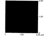
Fig. 6 is after cleaning with acid silicon dioxide CMP slurry (pH=0.8) chemically machinery polished 1 hour with diluted hydrofluoric acid, the AFM picture on GaN surface.
Fig. 7 is after cleaning with acid silicon dioxide CMP slurry (pH=0.8) chemically machinery polished 1 hour with diluted hydrofluoric acid, the scanning electronic microscope on GaN surface (SEM) photo.
Fig. 8 be with 1 μ m bortz powder slurry mechanical polishing after forming minute surface, the Normaski light micrograph (* 100) on GaN surface.
Fig. 9 is the AFM image on GaN shown in Figure 8 surface.
The detailed description and the embodiment preferred of invention
According to high quality Al of the present invention
xGa
yIn
zThe manufacturing of N wafer can be realized by the procedure of processing of hereinafter more complete description, comprises no supporting al
xGa
yIn
zThe half-finished manufacturing of N wafer, grinding, mechanical polishing, chemically machinery polished and reduce the step of internal stress.
Unsupported Al
xGa
yIn
zN wafer work in-process can be obtained by multiple appropriate means.A kind of method comprises the Al that at first grows
xGa
yIn
zThe N boule is cut to the wafer work in-process then.The another kind of Al that makes
xGa
yIn
zN wafer process of semi-finished may further comprise the steps: (1) grows into thick Al with appropriate means for example hydride evaporation phase epitaxy growth method (HVPE), organo-metallic muriate (MOC) method, organometallic chemistry evaporation deposition method (MOCVD), subliming method etc. on foreign substrate
xGa
yIn
zThe N film; (2) are by polishing or etching foreign substrate, by stripping technology or other suitable technology of induced with laser, by thick Al then
xGa
yIn
zRemove foreign substrate on the N film.
For instance, thickness is that the GaN film of about 400 μ m can grow on the Sapphire Substrate with HVPE method processing technology.
On these wafer work in-process, make marks, to differentiate the half-finished orientation of this crystal as the plane.Al
xGa
yIn
zN wafer work in-process can be made circle with for example particle beam, are beneficial to half-finished subsequent installation of described wafer or processing.
With unsupported Al
xGa
yIn
zN wafer work in-process are installed on the anchor clamps so that can carry out necessary grinding or polishing.Described wafer work in-process can be installed on the reeded mould to clamp this wafer work in-process.Perhaps, these wafer work in-process can be installed on the planar mould, heat this mould by for example (1) on hot-plate, (2) wax on mould and (3) press to the wafer work in-process on the mould that adds wax.After mold cools down, wax is cured, and has played the wafer work in-process are fixed on effect among the mould.
Work as Al
xGa
yIn
zN wafer work in-process are by Al
xGa
yIn
zThe N boule obtains with relative when thicker and even, and reeded mould can be used for setting off this wafer work in-process, is than short processes time, easier dismounting with than less contamination with respect to its advantage of the mould that adds wax.
On the other hand, to may being more crisp, thinner or at the uniform Al of its thickness low LCL
xGa
yIn
zN wafer work in-process, for example for the wafer work in-process that obtain by the HVPE method because grind and/or polishing during Al
xGa
yIn
zThe N wafer has broken danger, therefore can preferentially not select the mould of band groove for use.
Al is installed
xGa
yIn
zThe employed anchor clamps of N wafer work in-process can be any suitable suitable types and can be compatible with various grindings or polissoir.In order to improve Al
xGa
yIn
zN wafer thickness homogeneity can be used a kind of specificly, comprises the planar grinding clamp that three adjustable diamond plugs (stop) are constituted.Leaving chucking surface predetermined distance place, parallel by the plane that described plug is determined with this chucking surface.The Al of this predetermined distance definition for grinding
xGa
yIn
zThe minimum thickness of N wafer is because the effect of three diamond plugs is as stoping surfacing from Al
xGa
yIn
zThe arrests of removing on the N wafer.
At Al
xGa
yIn
zN wafer work in-process are owing to wherein exist internal stress and have slightly under the situation of bending or distortion, preferably set off in the process with wax in mould at this wafer a weight is placed on these wafer work in-process.To those skilled in the art, be easy to determine for type and the quantity that reaches the employed weight of this purpose.
At Al
xGa
yIn
zAfter N wafer work in-process are suitably set off, these wafer work in-process can be pressed to abrasive sheet, grind with the abrasive particle of implanting these abrasive sheet surfaces, to obtain wafer plane.Can regulate the wafer applied pressure, with the control grinding technics.
When using identical abrasive and abrasive sheet speed of rotation, Al
xGa
yIn
zThe half-finished grinding rate of N wafer improves with the increase of abrasive granular size.Bigger abrasive particle can bring higher grinding rate, but can produce more coarse lapped face.
Grinding rate also depends on the hardness of used abrasive material.For example, bortz powder has higher grinding rate than carborundum powder, and latter's ratio aluminum oxide powder has higher grinding rate.
Grinding rate also depends on the type of used abrasive sheet.For example, the copper abrasive sheet has lower grinding rate than cast iron abrasive sheet, but the copper abrasive sheet can produce more level and smooth lapped face than cast iron abrasive sheet.
In order to obtain best grinding result, need to consider multiple factor, for example situation of process period, surface grinding and manufacturing cost, and to take employed abrasive substance, granular size, grinding rate and wafer pressure in the present invention's practice into consideration.In order to reduce Al
xGa
yIn
zThe possibility of N broken wafers, the preferred use is lower than 5psi, the more preferably pressure of 2psi.In order to reduce process period, preferred grinding rate reaches the above cutting output of 50 μ m/hr.At various abrasive substances for example among diamond, silicon carbide, norbide and the aluminum oxide, preferred diamond slurry, this is because it has high material removing rate and can access surface appearance preferably.
Al
xGa
yIn
zThe half-finished grinding of N wafer can once be finished, and also can multistep carry out suddenly, and use reduces the abrasive of granular size in proper order in each follow-up grinding steps.After each grinding steps, use the observation by light microscope surface appearance, so that before carrying out next step, determine the previous step surface damage of basically eliminate.
In illustrative embodiment of the present invention, used simple ground slurry, comprising the diamond lap material of 9 μ m, under lpsi pressure, on the cast iron abrasive sheet, grind Al
xGa
yIn
zThe N wafer.Diamond lap material particulate size is provided by the producer of diamond slurry, and is the mean size of diamond particles in the slurry.
In another illustrative embodiment of the present invention, used two kinds of ground slurries: first kind of ground slurry comprises the diamond lap material of 9 μ m, grinds Al on the cast iron abrasive sheet
xGa
yIn
zThe N wafer; Second kind of slurry comprises the diamond lap material of 6 μ m, grinds same wafer on the copper abrasive sheet, obtains the ideal wafer surface.
At Al
xGa
yIn
zAfter the N wafer grinding, can carry out mechanical polishing to obtain level and smooth configuration of surface.In the mechanical polishing process, with described Al
xGa
yIn
zThe N wafer is pressed to the polishing pad with abrasive grains.Glossing can produce better condition of surface than grinding usually, even use the diamond slurry of identical size.Polishing can be passed through single stage method, or multistep processes realizes the abrasive grains size that use reduces successively in each follow-up polishing step.
After mechanical polishing process, Al
xGa
yIn
zIt is level and smooth relatively that the surface of N wafer becomes.Fig. 8 be with 1 μ m diamond slurry mechanical polishing after forming minute surface, the Normaski light micrograph (* 100) on GaN surface.But, this Al
xGa
yIn
zThe N wafer is not suitable for Al
xGa
yIn
zThe isoepitaxial growth of N crystalline is because the damage that it still has tangible surface and is suitable for.The feature of described surface damage is that intensive polishing scratch is arranged, and this scratch is a visible under atomic force microscope, as shown in Figure 9.
For remove these surfaces and be suitable for damage and polishing scratch, preferentially select for use Al
xGa
yIn
zThe N wafer carries out chemically machinery polished (CMP).Effectively to Al
xGa
yIn
zThe CMP slurry that the Ga-side of N wafer is carried out chemically machinery polished comprises acid and grinds and use amorphous silica particles that as fumed silica or colloid silica, its granular size is less than 200nm.This CMP pH value of slurry is in the scope of about 0.5-about 4.Preferred this CMP slurry also comprises oxygenant, as hydrogen peroxide, DICHLOROISOCYANURIC ACID etc.
Fig. 1 and 2 is Normaski light micrograph and the AFM image with the about 1 hour GaN wafer of the acidoid silica slurry chemically machinery polished of pH=0.8.Before CMP, described GaN wafer at first polishes with 1 μ m diamond slurry.A little defective on substrate, the GaN surface is very level and smooth, and the rms surface roughness is at 2 * 2 μ m
2Approximately 0.15nm on the area, at 10 * 10 μ m
2Approximately 0.5nm on the area.In addition, under AFM, the GaN phase step type structure of not seeing before can observing.The existence of this phase step type structure is CMP technology has successfully been removed the polishing scratch by aforementioned mechanical polishing a kind of indication.CMP speed when using this slurry for example can be on the order of magnitude of about 2 μ m/hr.
For further determine CMP processing removed should the surface surface damage down, in CMP processing back with strong etching reagent H
3PO
4In 180 ℃ of etchings 5 minutes.Under this etching condition, damage is more etched at faster speed than good crystalline material down for the crystal defect of GaN Ga-side and surface and surface, forms the etching pitting.The size of these pittings and number can be investigated with atomic force microscope.Through overheated H
3PO
4After the etching, the wafer of CMP polishing has some etching pittings, but the pitting consistent in density that the density of this etching pitting and CMP glazed surface show.But it is big that the size of described pitting becomes.Under the contrast, with CMP processing not fully (the promptly short CMP process period and so and kept polishing damage) of polishing be presented at and use H
3PO
4After 5 minutes, have more etching pitting in 180 ℃ of etchings, and many pittings are along a line, if this explanation CMP processes when incomplete, described surface and surface damage down can not be removed fully.
It is favourable adding oxygenant in acid CMP slurry.When with hydrogen peroxide, DICHLOROISOCYANURIC ACID during as oxygenant, polishing speed is about 2 μ m/hr, and the rms surface roughness is at 2 * 2 μ m
2Be lower than 0.2 on the area, at 10 * 10 μ m
2Be lower than 0.5nm on the area.Under AFM, can easily observe Al
xGa
yIn
zThe phase step type structure of N wafer.
Effectively to Al
xGa
yIn
zThe 2nd CMP slurry that the Ga-side of N wafer is carried out chemically machinery polished comprises that it is less than 200nm that colloidal alumina particle, granular size are used in acid and grinding.This CMP pH value of slurry is preferably in the scope of about 3-about 4.Preferred this CMP slurry also comprises oxygenant, as hydrogen peroxide, DICHLOROISOCYANURIC ACID etc.
Fig. 3 uses acidoid aluminum oxide CMP slurry (pH=3.6) chemically machinery polished after 1 hour, and the AFM picture on GaN surface contains hydrogen peroxide as oxygenant in the described slurry.Under AFM, observe the phase step type structure, illustrate that the acidoid alumina slurry is effective for the physical abuse of removing the GaN surface.But under same polishing operation condition, the slurry of colloidal alumina-Ji is than its polishing speed of slurry of silicon-dioxide-Ji much smaller (about 0.1 μ m/hr).Because polishing velocity is slow, many polishing scratches still exist after polishing 1 hour with acidoid aluminum oxide CMP slurry.Therefore the slurry with colloidal alumina-Ji needs long polishing time could remove surface/subsurface damage fully.
Effectively to Al
xGa
yIn
zThe 3rd CMP slurry that the Ga-side of N wafer is carried out chemically machinery polished comprises alkali and amorphous silica particles, or fumed silica or colloid silica, and granular size is less than 200nm.This CMP pH value of slurry is in the scope of about 8-about 13.5.
Figure 4 and 5 are to use the basoid silicon-dioxide CMP slurry chemical mechanical of pH=11.2 to polish after 1 hour the Normaski light micrograph of GaN wafer surface and AFM image.Compare with the resulting condition of surface of acid silicon dioxide slurry, the surface after the polishing is more coarse and more scratch obviously arranged.And, to compare with the GaN surface after the diamond slurry mechanical polishing of the bortz powder that contains 1 μ m with GaN is surperficial, described scratch is bigger darker, and this explanation exists larger particle or particle aggregation in alkaline silica slurry.Interesting is also can observe the phase step type structure.The surface damage that the existence explanation front mechanical polishing of phase step type structure is produced has been removed, but exists bigger particle to cause new damage in slurry.Therefore, in order to remove bigger particle, less than 200nm, need to filter alkaline silica slurry with the granular size of guaranteeing the abrasive grains in this slurry.
Except regulating the pH pH value that can also regulate alkaline silica slurry with ammonia or alkanolamine with oxyhydroxide.Ammonia-or alkanolamine-stable slurry more level and smooth glazed surface can be provided, therefore more preferably than the slurry of oxyhydroxide-Ji.
In order to improve the stability of CMP technology, it is favourable controlling ambient moisture and temperature in the CMP technological process well.
After chemically machinery polished, available technology known in the art is with Al
xGa
yIn
zN chip cleaning and drying.The etching of available appropriateness is removed any residual surface and surface damage down from last polished wafer.Select appropriate etched condition, do not remove some residual surface damages so that have etching by last polishing or only etch on the wafer Ga-side of the limited extent that does not damage the Ga-side surface.The etching of this appropriateness also may be removed the damage of N-side surface, the stress that causes in wafer with the damage that reduces by the N-surface.The etching of this appropriateness also may obtain coarse N-configuration of surface.For example can be with this wafer at the aqueous solution of alkali (for example KOH or NaOH) or acid (HF for example, H
2SO
4Or H
3PO
4) the aqueous solution in, carry out etching slightly being lower than under 100 ℃ the temperature.
Al
xGa
yIn
zThe N wafer need bear the effect of internal stress, and this internal stress can cause the crooked or distortion of wafer.Before the manufacturing processed of this wafer, afterwards or between the manufacturing step to Al
xGa
yIn
zThe N wafer carries out thermal annealing or chemical milling, can alleviate this internal stress thus.
At described Al
xGa
yIn
zThere is big pitting on the surface of N wafer and has assembled in described pitting in manufacturing processed under the situation of pollutent, carries out chemical milling and cleaning, so that remove pollutent in by pitting between the step of wafer manufacturing.
In one embodiment of the invention, Al
xGa
yIn
zThe N wafer carries out thermal annealing under up to 1000 ℃ temperature in nitrogen atmosphere.Preferably, annealing temperature is at about 700 ℃-about 1000 ℃, and the time of thermal annealing is in about 1 minute-about 1 hour scope.
In another embodiment of the present invention, with Al
xGa
yIn
zThe N wafer carries out chemical milling, and preferably this etching can be by Al
xGa
yIn
zRemove the surfacing of damage on the N wafer, and reduce wafer bending and the distortion that causes by surface damage.
Al
xGa
yIn
zThe chemical milling of N wafer can be at high temperature, wafer is immersed in very strong acid or the alkali finishes.More than 150 ℃ the time, but sulfuric acid and phosphoric acid etching Al
xGa
yIn
zThe N wafer.In addition, but also etching Al of fused potassium hydroxide or sodium hydroxide
xGa
yIn
zThe N wafer.Etching condition preferably is controlled at as etched temperature and time and can removes under the condition of thickness less than 100 μ m surfacings, under the condition of preferred thickness less than 10 μ m.
In the mechanical polishing of GaN surface chemistry, for example to use after acid silicon dioxide CMP slurry (pH=0.8) handled 1 hour, pitting may appear, and this may be because the tomography of GaN wafer lattice causes.The diameter of described pitting is usually less than 1 μ m, more typically is to be lower than 0.5 μ m.With the atomic force microscope imaging time, there is not clearly border around the described pitting.Finish CMP polishing and for example use phosphoric acid after 150 ℃ of chemical millings 5 minutes when wafer, the size of pitting increases, but density remains unchanged, and does not promptly produce more pitting.Further, with the atomic force microscope imaging time, the described pitting that produces on the wafer of etching CMP polishing is seemingly hexagonal.
Fig. 6 is the AFM picture on GaN surface, and clearly visible pitting is arranged.Described GaN uses acidoid silicon-dioxide CMP slurry (pH=0.8) chemically machinery polished 1 hour in the surface.
Fig. 7 is scanning electronic microscope (SEM) picture of GaN wafer, and this wafer has clearly visible pitting with acidoid silicon-dioxide CMP slurry (pH=0.8) chemically machinery polished 1 hour, can measure the defect concentration of these GaN wafers to these pitting countings.Do not pass through the GaN surface of chemically machinery polished, do not observe this pitting with AFM or SEM.
With CMP prepared Al
xGa
yIn
zThe N wafer can make crystal defect reveal, so that afterwards with AFM or its defect concentration of SEM technical measurement.
This technology that defective is revealed is better than for example other technology of transmission electron microscope (SEM), wet chemical etching and chemical etching photograph.These etching techniques are carried out under the etching condition of harshness usually, make the Al after the etching
xGa
yIn
zThe N wafer is not suitable for Al
xGa
yIn
zThe epitaxy thereon that the N crystalline material is follow-up.
In contrast, use CMP technology reveals crystal defect and does not damage Al
xGa
yIn
zTherefore the crystal surface of N wafer can carry out follow-up crystalline growth.
Embodiment 1
The GaN film of hundreds of micron thickness is grown by HVPE technology on Sapphire Substrate, then by separating on the Sapphire Substrate.Obtained formed nothing and supported GaN wafer work in-process, demonstrated coarse Ga-surface, the RMS roughness is at 2 * 2 μ m
2Approximately 4nm on the area.
Then, the half-finished Ga-side of GaN wafer is polished with the acid silicon dioxide slurry, but do not carry out grinding technics.
After the polishing, the configuration of surface that can observe these GaN wafers is improved, and coarse surface is removed fully.The RMS roughness drops at 2 * 2 μ m
2Be lower than 0.3nm on the area.
Embodiment 2
Thickness at the thick GaN film of 200-500 micrometer range 2 " on the Sapphire Substrate, grow by HVPE technology, then by separating the GaN film on the Sapphire Substrate.Obtain formed nothing and supported GaN wafer work in-process.
The plane of GaN film is made marks when leaving 30 ° on Sapphire Substrate plane.Then, spray with particle beam that GaN wafer work in-process are made diameter is 30,35 and the wafer shape of 40mm.In order to prevent that wafer from breaking in making processes, preferably wafer is set off and be at least on the thick sheet glass of 1mm with wax.
9 GaN wafers are installed on the grinding clamp with wax, make its N-side grinding clamp.After the wax cooling, bloom is placed on the top of each wafer.At first grind on the cast iron abrasive sheet with the diamond slurry of 9 μ m diameters in the Ga-of GaN wafer side.Before grinding, its thickness has more different between the wafer and in each wafer.After grinding, the homogeneity of wafer thickness is greatly improved.
Then, wafer by taking out in the grinding clamp, and is fixed on the mechanical polishing anchor clamps with wax.Each wafer polishes with the diamond slurry of 3 μ m diameters, up to forming minute surface.In the opticmicroscope test, the surface damage that all grinding technics cause is all removed.
After mechanical polishing, wafer is carried out chemically machinery polished with the acidoid silica slurry.The Nomaski opticmicroscope is used to test polished surface, has removed all mechanical polishing scratches to confirm CMP technology.
Embodiment 3
3 GaN wafer work in-process are installed on the grinding clamp with wax, make its Ga-side grinding clamp.After the wax cooling, bloom is placed on the top of each wafer.At first use Lapmaster 15 mills, grind on the cast iron abrasive sheet with the diamond slurry of 9 μ m diameters, up to forming coarse homogeneous surface in the N-of GaN wafer side.
The N-side grind finish after, by with the hot-plate heating, with wafer by taking out in the grinding clamp.Clean wafer, and the GaN film set off in grinding clamp with wax, make its N-side to grinding clamp.After the wax cooling, bloom is placed on the top of each wafer.On the cast iron abrasive sheet, grind with the diamond slurry of 9 μ m diameters in the Ga-of GaN wafer side, up to obtaining required wafer thickness.Then, this GaN wafer grinds on the copper abrasive sheet with the diamond slurry of 6 μ m diameters, formed surface property in having removed aforementioned grinding steps.
After the grinding, described three wafers polish on the BuehlerECOMET polishing machine with the diamond slurry of 1 μ m diameter, formed surface property in having removed aforementioned grinding steps.
After mechanical polishing, described three wafers are carried out chemically machinery polished with the acidoid silica slurry on Buehler ECOMET polishing machine, described acidoid silica slurry prepares by 2 part of 1 mole hydrochloride aqueous solution of mixing and 1 part of commodity silica slurry (Nalco2350 polishing slurries).The Nomaski opticmicroscope is used to test polished surface, has removed all mechanical polishing scratches to confirm CMP technology.
After CMP technology, with described wafer by taking out in the polishing clamp, and cleaning.Wafer can clean with dilute hydrochloric acid, to remove any residual colloidal silica particles of wafer surface.This wafer is with atomic force microscope (Digital Instruments NanoScope III) imaging, with density and the surperficial smoothness of determining pitting.For a wafer, the RMS roughness is at 2 * 2 μ m
2On the area 0.11nm, at 10 * 10 μ m
2On the area 0.28nm.The little pit density of three wafers approximately is 10
6-10
7Hole/cm
2, the size in hole approximately is less than 0.4 μ m diameter.
GaN wafer of the present invention can be used for making up opto-electronic device such as photodiode and blue streak laser apparatus.(LED ' s) and laser apparatus are start-up technique because the blue streak emitting diode, so these devices are important, it magnetic-light is stored and the storage density of CDROM higher, and can make up the indicating meter of launching panchromatic light.The alternative incandescent light that among highway and railway signal lamp etc., uses at present of these devices, but they have very actual cost and save energy.
The invention describes specific characteristic, aspect and embodiment.Be understandable that suitability of the present invention is not limited to, and be easy to expand to and comprise its various variants, modification and other embodiment that this is that those skilled in the art itself are easy to accomplish.Correspondingly, the present invention can broadly explain, and is consistent with the determined scope of accompanying Claim book.
Claims (50)
1. one kind contains Al
xGa
yIn
zThe wafer of N, wherein 0<y≤1 and x+y+z=1, described wafer have the Ga side surface of essentially no polishing scratch and it is characterized in that its rootmean-square surfaceness in the Ga-of wafer side at 10 * 10 μ m
2On the area less than 1nm.
2. the wafer of claim 1, the rootmean-square surfaceness of wherein said wafer Ga-side is at 10 * 10 μ m
2On the area less than 0.7nm.
3. the wafer of claim 1, the rootmean-square surfaceness of wherein said wafer Ga-side is at 10 * 10 μ m
2On the area less than 0.5nm.
4. the wafer of claim 1, the rootmean-square surfaceness of wherein said wafer Ga-side is at 2 * 2 μ m
2On the area less than 0.4nm.
5. the wafer of claim 1, the rootmean-square surfaceness of wherein said wafer Ga-side is at 2 * 2 μ m
2On the area less than 0.2nm.
6. the wafer of claim 1, the rootmean-square surfaceness of wherein said wafer Ga-side is at 2 * 2 μ m
2On the area less than 0.15nm.
7. the wafer of claim 1 is the phase step type structure in its Ga-side when it is characterized in that with atomic force microscope observation.
8. the wafer of claim 1 is characterized in that the lattice defect in described Ga-side is the visible pitting, and its diameter is less than 1 μ m.
9. the wafer of claim 1, this wafer are by with containing the chemical mechanical polishing slurry of silicon-dioxide or aluminum oxide to Al
xGa
yIn
zThe N wafer carries out chemically machinery polished and forms on its Ga-side.
10. epitaxially grown Al
xGa
yIn
zN crystalline texture is comprising containing Al
xGa
yIn
zEpitaxially grown Al on the N wafer
X 'Ga
Y 'In
Z 'The film of N, 0<y≤1 wherein, x+y+z=1,0<y '≤1 and x '+y '+z '=1, described wafer have the Ga side surface of essentially no polishing scratch and it is characterized in that its rootmean-square surfaceness in the Ga-of wafer side at 10 * 10 μ m
2On the area less than 1nm.
11. the epitaxy Al of claim 10
xGa
yIn
zN crystalline texture is comprising the wurtzite crystalline membrane.
12. the epitaxially grown Al of claim 10
xGa
yIn
zN crystalline texture, wherein epitaxially grown Al
X 'Ga
Y 'In
Z 'The N film with contain Al
xGa
yIn
zThe wafer of N has identical composition.
13. the epitaxially grown Al of claim 10
xGa
yIn
zN crystalline texture, wherein epitaxially grown Al
X 'Ga
Y 'In
Z 'The N film with contain Al
xGa
yIn
zThe wafer of N has different compositions.
14. the epitaxially grown Al of claim 10
xGa
yIn
zN crystalline texture, wherein epitaxially grown Al
X 'Ga
Y 'In
Z 'The N film is made up of fractionated.
15. comprising, opto-electronic device, this device at least aly containing Al
xGa
yIn
zThe extension Al that grows on the N wafer
X 'Ga
Y 'In
Z 'The N crystalline structure, wherein, x '+y '+z '=1, wherein 0<y≤1 and x+y+z=1, described wafer have the Ga side surface of essentially no polishing scratch and it is characterized in that its rootmean-square surfaceness in the Ga-of this wafer side at 10 * 10 μ m
2On the area less than 1nm.
16. the opto-electronic device of claim 15, opto-electronic device wherein is a photodiode.
17. the opto-electronic device of claim 15, opto-electronic device wherein is a blue light laser diode.
18. the opto-electronic device of claim 15, opto-electronic device wherein is added into photodiode.
19. the opto-electronic device of claim 15, opto-electronic device wherein is added into magnetic-optical memory.
20. the opto-electronic device of claim 15, opto-electronic device wherein are added into panchromatic active display light source.
21. the opto-electronic device of claim 15, opto-electronic device wherein is added into DVD equipment.
22. comprising, microelectronic device, this device at least aly containing Al
xGa
yIn
zThe extension Al that grows on the N wafer
X 'Ga
Y 'In
Z 'The N crystalline structure, wherein, x '+y '+z '=1, wherein 0<y≤1 and x+y+z=1, described wafer have the Ga side surface of essentially no polishing scratch and it is characterized in that its rootmean-square surfaceness in the Ga-of this wafer side at 10 * 10 μ m
2On the area less than 1nm.
23. epitaxially grown Al
X 'Ga
Y 'In
Z 'N crystalline boule, wherein, x '+y '+z '=1, described boule is to contain Al
xGa
yIn
zEpitaxially grown on the N wafer, wherein 0<y≤1 and x+y+z=1, described wafer have the Ga side surface of essentially no polishing scratch and it is characterized in that its rootmean-square surfaceness in the Ga-of this wafer side at 10 * 10 μ m
2On the area less than 1nm.
24. the epitaxially grown Al of claim 23
X 'Ga
Y 'In
Z 'N crystalline boule, described boule is grown in gas phase.
25. the epitaxially grown Al of claim 23
X 'Ga
Y 'In
Z 'N crystalline boule, described boule is grown in liquid phase.
Contain Al 26. make
xGa
yIn
zThe method of N wafer, wherein 0<y≤1 and x+y+z=1, this method may further comprise the steps:
Al is provided
xGa
yIn
zN wafer work in-process, its thickness is in 100 μ m-1000 mu m ranges;
Optionally reduce described Al
xGa
yIn
zThe internal stress of N wafer;
Optionally grind Al with ground slurry
xGa
yIn
zThe half-finished N-side of N wafer, described ground slurry contain the abrasive of mean particle size in 5 μ m-15 mu m ranges;
With mechanical polishing material this Al of mechanical polishing optionally
xGa
yIn
zThe half-finished N-side of N wafer, described mechanical polishing material contain the abrasive of mean particle size in 0.1 μ m-6 mu m range;
Optionally grind Al with ground slurry
xGa
yIn
zThe half-finished Ga-side of N wafer, described ground slurry contain the abrasive of mean particle size in 5 μ m-15 mu m ranges;
With this Al of mechanical polishing material mechanical polishing
xGa
yIn
zThe half-finished Ga-side of N wafer, described mechanical polishing material contain the abrasive of mean particle size in 0.1 μ m-6 mu m range;
With chemical mechanical polishing slurry chemically machinery polished Al
xGa
yIn
zThe half-finished Ga-side of N wafer, described chemical mechanical polishing slurry contain at least a chemical reactant and the mean particle size abrasive grains less than 200nm; With
In order to improve its surface quality, etching Al under the etching condition of gentleness optionally
xGa
yIn
zThe N wafer is further to reduce Al
xGa
yIn
zThe internal stress of N wafer obtains the uneven surface of N-side;
The Al that makes wherein like this
xGa
yIn
zThe N wafer is at 10 * 10 μ m in the rootmean-square surfaceness of its Ga-side
2On the area less than 1nm.
27. the method for claim 26, wherein Al
xGa
yIn
zN wafer work in-process can be produced as follows:
On foreign substrate, grow into thick Al
xGa
yIn
zThe N film; With
With this thick Al
xGa
yIn
zThe N film is by taking off on the described foreign substrate.
28. the method for claim 26, wherein Al
xGa
yIn
zN wafer work in-process can be produced as follows:
Grow into Al
xGa
yIn
zThe N boule; With
Cut described Al
xGa
yIn
zThe N boule.
29. the method for claim 28 is wherein cut Al
xGa
yIn
zThe N boule, the wafer surface of semi-finished that obtains is perpendicular to the c-axle.
30. the method for claim 28 is wherein cut Al
xGa
yIn
zThe N boule has a mind to make the wafer surface of semi-finished to be not orthogonal to the c-axle.
31. the method for claim 26, wherein by making described wafer under 700 ℃-1000 ℃ high temperature, thermal annealing 1 minute-1 hour in nitrogen or ammonia environment and reduce described Al
xGa
yIn
zThe internal stress of N wafer.
32. the method for claim 26, wherein Al
xGa
yIn
zThe internal stress of N wafer can reduce by described wafer is carried out chemical milling, consequently can be by removing the surfacing of thickness less than 100 μ m on the described wafer.
33. the method for claim 32 wherein can be by described Al
xGa
yIn
zRemove the surfacing of thickness on the N wafer less than 10 μ m.
34. the method for claim 32, wherein said Al
xGa
yIn
zThe N wafer carries out chemical milling with strong acid under the temperature more than 150 ℃.
35. the method for claim 34, wherein said strong acid are selected from sulfuric acid, phosphoric acid or its combination.
36. the method for claim 32, wherein Al
xGa
yIn
zThe N wafer carries out chemical milling with strong molten caustic soda under the temperature more than 150 ℃.
37. the method for claim 36, wherein said highly basic are selected from fusion LiOH, fusion NaOH, fusion KOH, fusion RbOH, fusion CsOH, or its combination.
38. the method for claim 26, wherein said Al
xGa
yIn
zN wafer work in-process grind with ground slurry, and described ground slurry contains the abrasive that is selected from bortz powder, carborundum powder, boron carbide powder and aluminum oxide powder.
39. the method for claim 26, wherein said ground slurry contain the bortz powder that mean particle size is 6 μ m-10 μ m.
40. the method for claim 26, wherein said Al
xGa
yIn
zThe half-finished Ga-side of N wafer is ground with two kinds or multiple ground slurry, and each follow-up ground slurry correspondingly contains the littler abrasive of mean size.
41. the method for claim 40, wherein said Al
xGa
yIn
zN wafer work in-process are earlier with containing first ground slurry grinding that mean size is 8 μ m-10 μ m abrasives, then with containing second ground slurry grinding that mean size is 5 μ m-7 μ m abrasives.
42. the method for claim 26, wherein said mechanical polishing material contains the abrasive that is selected from bortz powder, carborundum powder, boron carbide powder and aluminum oxide powder.
43. the method for claim 26, wherein mechanical polishing material contains the bortz powder that mean particle size is 0.1 μ m-6 μ m.
44. the method for claim 26, wherein said Al
xGa
yIn
zN wafer work in-process carry out mechanical polishing with two kinds or multiple mechanical polishing material, and each follow-up mechanical polishing material contains the abrasive that mean size reduces in proper order.
45. the method for claim 44, wherein said Al
xGa
yIn
zN wafer work in-process are earlier with containing the first mechanical polishing material mechanical polishing that mean size is 2.5 μ m-3.5 μ m abrasives, then with containing the second mechanical polishing material mechanical polishing that mean size is 0.75 μ m-1.25 μ m abrasive, again with containing the 3rd mechanical polishing material mechanical polishing that mean size is 0.35 μ m-0.65 μ m abrasive, again with containing the 4th mechanical polishing material mechanical polishing that mean size is 0.2 μ m-0.3 μ abrasive, again with containing the 5th mechanical polishing material mechanical polishing that mean size is 0.1 μ m-0.2 μ m abrasive.
46. the method for claim 26, wherein said chemical mechanical polishing slurry is a tart, and the pH value of described chemical mechanical polishing slurry is in the scope of 0.5-4.
47. the method for claim 26, wherein said chemical mechanical polishing slurry is alkaline, and the pH value of described chemical mechanical polishing slurry is in the scope of 8-13.5.
48. being selected from, the method for claim 26, the etching condition of wherein said gentleness be lower than under 100 ℃ the temperature etching and etching in the aqueous solution of alkali in aqueous acid.
49. the method for claim 48, wherein said acid is selected from the aqueous solution of hydrofluoric acid, nitric acid, sulfuric acid, phosphoric acid, and their combination.
50. the method for claim 48, wherein said alkali is selected from the aqueous solution of LiOH, NaOH, KOH, RbOH, CsOH, and their combination.
Applications Claiming Priority (2)
| Application Number | Priority Date | Filing Date | Title |
|---|---|---|---|
| US09/877,437 US6488767B1 (en) | 2001-06-08 | 2001-06-08 | High surface quality GaN wafer and method of fabricating same |
| US09/877,437 | 2001-06-08 |
Related Child Applications (1)
| Application Number | Title | Priority Date | Filing Date |
|---|---|---|---|
| CN200710186509XA Division CN101220244B (en) | 2001-06-08 | 2002-06-04 | High surface quality GaN wafer and method of fabricating same |
Publications (2)
| Publication Number | Publication Date |
|---|---|
| CN1541287A CN1541287A (en) | 2004-10-27 |
| CN100465356C true CN100465356C (en) | 2009-03-04 |
Family
ID=25369959
Family Applications (2)
| Application Number | Title | Priority Date | Filing Date |
|---|---|---|---|
| CNB028114140A Expired - Lifetime CN100465356C (en) | 2001-06-08 | 2002-06-04 | High surface quality GaN wafer and method of fabricating same |
| CN200710186509XA Expired - Lifetime CN101220244B (en) | 2001-06-08 | 2002-06-04 | High surface quality GaN wafer and method of fabricating same |
Family Applications After (1)
| Application Number | Title | Priority Date | Filing Date |
|---|---|---|---|
| CN200710186509XA Expired - Lifetime CN101220244B (en) | 2001-06-08 | 2002-06-04 | High surface quality GaN wafer and method of fabricating same |
Country Status (8)
| Country | Link |
|---|---|
| US (3) | US6488767B1 (en) |
| EP (2) | EP1404902B1 (en) |
| JP (7) | JP4350505B2 (en) |
| KR (2) | KR100959084B1 (en) |
| CN (2) | CN100465356C (en) |
| MY (1) | MY127915A (en) |
| TW (1) | TWI226391B (en) |
| WO (1) | WO2002101121A1 (en) |
Families Citing this family (206)
| Publication number | Priority date | Publication date | Assignee | Title |
|---|---|---|---|---|
| US5679152A (en) * | 1994-01-27 | 1997-10-21 | Advanced Technology Materials, Inc. | Method of making a single crystals Ga*N article |
| US20040134873A1 (en) * | 1996-07-25 | 2004-07-15 | Li Yao | Abrasive-free chemical mechanical polishing composition and polishing process containing same |
| US6596079B1 (en) * | 2000-03-13 | 2003-07-22 | Advanced Technology Materials, Inc. | III-V nitride substrate boule and method of making and using the same |
| RU2296189C2 (en) * | 2001-06-06 | 2007-03-27 | АММОНО Сп.з о.о. | Method and apparatus for producing three-dimensional monocrystalline gallium-containing nitride (variants) |
| US6488767B1 (en) * | 2001-06-08 | 2002-12-03 | Advanced Technology Materials, Inc. | High surface quality GaN wafer and method of fabricating same |
| US7067849B2 (en) | 2001-07-17 | 2006-06-27 | Lg Electronics Inc. | Diode having high brightness and method thereof |
| JP2003063897A (en) * | 2001-08-28 | 2003-03-05 | Sony Corp | Nitride-based iii-v group compound semiconductor substrate and method for producing the same, method for producing light emitting device of semiconductor and method for producing semiconductor device |
| US6949395B2 (en) * | 2001-10-22 | 2005-09-27 | Oriol, Inc. | Method of making diode having reflective layer |
| KR100904501B1 (en) | 2001-10-26 | 2009-06-25 | 암모노 에스피. 제트오. 오. | Substrate for epitaxy |
| US7148520B2 (en) | 2001-10-26 | 2006-12-12 | Lg Electronics Inc. | Diode having vertical structure and method of manufacturing the same |
| WO2003036771A1 (en) * | 2001-10-26 | 2003-05-01 | Ammono Sp.Zo.O. | Nitride semiconductor laser element, and production method therefor |
| US20060005763A1 (en) * | 2001-12-24 | 2006-01-12 | Crystal Is, Inc. | Method and apparatus for producing large, single-crystals of aluminum nitride |
| US8545629B2 (en) | 2001-12-24 | 2013-10-01 | Crystal Is, Inc. | Method and apparatus for producing large, single-crystals of aluminum nitride |
| US7638346B2 (en) * | 2001-12-24 | 2009-12-29 | Crystal Is, Inc. | Nitride semiconductor heterostructures and related methods |
| US8809867B2 (en) * | 2002-04-15 | 2014-08-19 | The Regents Of The University Of California | Dislocation reduction in non-polar III-nitride thin films |
| WO2003089696A1 (en) * | 2002-04-15 | 2003-10-30 | The Regents Of The University Of California | Dislocation reduction in non-polar gallium nitride thin films |
| JP2003327497A (en) * | 2002-05-13 | 2003-11-19 | Sumitomo Electric Ind Ltd | GaN SINGLE CRYSTAL SUBSTRATE, NITRIDE-BASED SEMICONDUCTOR EPITAXIAL SUBSTRATE, NITRIDE-BASED SEMICONDUCTOR DEVICE AND METHOD OF PRODUCING THE SAME |
| TWI274735B (en) * | 2002-05-17 | 2007-03-01 | Ammono Sp Zoo | Bulk single crystal production facility employing supercritical ammonia |
| US20060138431A1 (en) * | 2002-05-17 | 2006-06-29 | Robert Dwilinski | Light emitting device structure having nitride bulk single crystal layer |
| PL225427B1 (en) * | 2002-05-17 | 2017-04-28 | Ammono Spółka Z Ograniczoną Odpowiedzialnością | Light emitting element structure having nitride bulk single crystal layer |
| CN100339512C (en) * | 2002-06-26 | 2007-09-26 | 波兰商艾蒙诺公司 | Improvemrnt of process for obtaining of bulk monocrystallline gallium-containing nitride |
| KR100485169B1 (en) * | 2002-10-09 | 2005-04-22 | 동부아남반도체 주식회사 | Method of polishing semiconductor device |
| TWI334890B (en) | 2002-12-11 | 2010-12-21 | Ammono Sp Zoo | Process for obtaining bulk mono-crystalline gallium-containing nitride, eliminating impurities from the obtained crystal and manufacturing substrates made of bulk mono-crystalline gallium-containing nitride |
| PL225423B1 (en) * | 2002-12-11 | 2017-04-28 | Ammono Spółka Z Ograniczoną Odpowiedzialnością | Method of producing substrate standardized with epitaxial layer (template type substrates) from voluminal mono-crystalline nitride containing gallium with surface of high structural quality |
| PL224991B1 (en) * | 2002-12-11 | 2017-02-28 | Ammono Spółka Z Ograniczoną Odpowiedzialnością | A substrate for epitaxy and a method of preparing the same |
| US7221037B2 (en) * | 2003-01-20 | 2007-05-22 | Matsushita Electric Industrial Co., Ltd. | Method of manufacturing group III nitride substrate and semiconductor device |
| JP4052150B2 (en) * | 2003-03-05 | 2008-02-27 | 住友電気工業株式会社 | Manufacturing method of nitride semiconductor device |
| JP4511801B2 (en) * | 2003-03-14 | 2010-07-28 | 株式会社リコー | Group III nitride crystal polishing method, group III nitride crystal and semiconductor device |
| JP5096677B2 (en) | 2003-04-15 | 2012-12-12 | ザ リージェンツ オブ ザ ユニバーシティ オブ カリフォルニア | Nonpolar (Al, B, In, Ga) N quantum well |
| KR100550491B1 (en) * | 2003-05-06 | 2006-02-09 | 스미토모덴키고교가부시키가이샤 | Nitride semiconductor substrate and processing method of nitride semiconductor substrate |
| US20060012011A1 (en) * | 2003-06-16 | 2006-01-19 | Seiji Nakahata | Mehtod for processing nitride semiconductor crystal surface and nitride semiconductor crystal obtained by such method |
| US7170095B2 (en) * | 2003-07-11 | 2007-01-30 | Cree Inc. | Semi-insulating GaN and method of making the same |
| JP4276020B2 (en) * | 2003-08-01 | 2009-06-10 | 豊田合成株式会社 | Method for producing group III nitride compound semiconductor |
| JP2005112641A (en) * | 2003-10-03 | 2005-04-28 | Sumitomo Electric Ind Ltd | Nitride semiconductor substrate and method for manufacturing nitride semiconductor substrate |
| CN100552888C (en) * | 2003-10-27 | 2009-10-21 | 住友电气工业株式会社 | Gallium nitride semiconductor substrate and manufacture method thereof |
| JP4232605B2 (en) * | 2003-10-30 | 2009-03-04 | 住友電気工業株式会社 | Nitride semiconductor substrate manufacturing method and nitride semiconductor substrate |
| JP4534631B2 (en) * | 2003-10-31 | 2010-09-01 | 住友電気工業株式会社 | Method for producing group III nitride crystal |
| US7276779B2 (en) | 2003-11-04 | 2007-10-02 | Hitachi Cable, Ltd. | III-V group nitride system semiconductor substrate |
| US7323256B2 (en) * | 2003-11-13 | 2008-01-29 | Cree, Inc. | Large area, uniformly low dislocation density GaN substrate and process for making the same |
| DE102004010379A1 (en) * | 2004-03-03 | 2005-09-22 | Schott Ag | Process for the production of wafers with low-defect surfaces, the use of such wafers and electronic components obtained therefrom |
| WO2005099057A1 (en) * | 2004-03-31 | 2005-10-20 | Nec Corporation | Wafer for nitride semiconductor light emitting element, manufacturing method thereof and nitride semiconductor light emitting element obtained from the wafer |
| US20080261401A1 (en) * | 2004-04-08 | 2008-10-23 | Ii-Vi Incorporated | Chemical-Mechanical Polishing of Sic Surfaces Using Hydrogen Peroxide or Ozonated Water Solutions in Combination with Colloidal Abrasive |
| KR100718188B1 (en) * | 2004-05-07 | 2007-05-15 | 삼성코닝 주식회사 | Non-polar single crystalline a-plane nitride semiconductor wafer and preparation thereof |
| JP5116305B2 (en) * | 2004-05-11 | 2013-01-09 | ニッタ・ハース株式会社 | Polishing composition and substrate polishing method |
| US7956360B2 (en) * | 2004-06-03 | 2011-06-07 | The Regents Of The University Of California | Growth of planar reduced dislocation density M-plane gallium nitride by hydride vapor phase epitaxy |
| PL1769105T3 (en) * | 2004-06-11 | 2014-11-28 | Ammono S A | Bulk mono-crystalline gallium nitride and method for its preparation |
| EP1605498A1 (en) * | 2004-06-11 | 2005-12-14 | S.O.I. Tec Silicon on Insulator Technologies S.A. | A method of manufacturing a semiconductor wafer |
| JP4525309B2 (en) * | 2004-11-19 | 2010-08-18 | 日立電線株式会社 | Method for evaluating group III-V nitride semiconductor substrate |
| PL371405A1 (en) | 2004-11-26 | 2006-05-29 | Ammono Sp.Z O.O. | Method for manufacture of volumetric monocrystals by their growth on crystal nucleus |
| US7313965B2 (en) * | 2004-12-27 | 2008-01-01 | General Electric Company | High-temperature pressure sensor |
| US7527742B2 (en) * | 2005-06-27 | 2009-05-05 | Momentive Performance Materials Inc. | Etchant, method of etching, laminate formed thereby, and device |
| JP5065574B2 (en) * | 2005-01-12 | 2012-11-07 | 住友電気工業株式会社 | Polishing method of GaN substrate |
| JP2006261649A (en) * | 2005-02-21 | 2006-09-28 | Mitsubishi Chemicals Corp | Nitride semiconductor material and method of manufacturing nitride semiconductor crystal |
| US20090026488A1 (en) * | 2005-02-21 | 2009-01-29 | Mitsubishi Chemical Corporation | Nitride semiconductor material and production process of nitride semiconductor crystal |
| JP4849296B2 (en) * | 2005-04-11 | 2012-01-11 | 日立電線株式会社 | GaN substrate |
| JP4244953B2 (en) * | 2005-04-26 | 2009-03-25 | 住友電気工業株式会社 | Light emitting device and manufacturing method thereof |
| JP4792802B2 (en) * | 2005-04-26 | 2011-10-12 | 住友電気工業株式会社 | Surface treatment method of group III nitride crystal |
| DE102005021099A1 (en) * | 2005-05-06 | 2006-12-07 | Universität Ulm | GaN layers |
| US20110018105A1 (en) * | 2005-05-17 | 2011-01-27 | Sumitomo Electric Industries, Ltd. | Nitride-based compound semiconductor device, compound semiconductor device, and method of producing the devices |
| JP2006352075A (en) * | 2005-05-17 | 2006-12-28 | Sumitomo Electric Ind Ltd | Cleaning method and manufacturing method for nitride compound semiconductor, and compound semiconductor, and board |
| US20060288929A1 (en) * | 2005-06-10 | 2006-12-28 | Crystal Is, Inc. | Polar surface preparation of nitride substrates |
| JP4363368B2 (en) * | 2005-06-13 | 2009-11-11 | 住友電気工業株式会社 | Method for evaluating damage to compound semiconductor member, and method for producing compound semiconductor member |
| JP4277826B2 (en) * | 2005-06-23 | 2009-06-10 | 住友電気工業株式会社 | Nitride crystal, nitride crystal substrate, nitride crystal substrate with epi layer, and semiconductor device and method for manufacturing the same |
| JP4518209B1 (en) | 2009-09-07 | 2010-08-04 | 住友電気工業株式会社 | Group III nitride crystal substrate, group III nitride crystal substrate with epi layer, and semiconductor device and method for manufacturing the same |
| US9708735B2 (en) | 2005-06-23 | 2017-07-18 | Sumitomo Electric Industries, Ltd. | Group III nitride crystal substrate, epilayer-containing group III nitride crystal substrate, semiconductor device and method of manufacturing the same |
| US8771552B2 (en) * | 2005-06-23 | 2014-07-08 | Sumitomo Electric Industries, Ltd. | Group III nitride crystal substrate, epilayer-containing group III nitride crystal substrate, semiconductor device and method of manufacturing the same |
| US20090029631A1 (en) * | 2005-09-23 | 2009-01-29 | General Electric | Mitigation of stress corrosion and fatigue by surface conditioning |
| US8349077B2 (en) | 2005-11-28 | 2013-01-08 | Crystal Is, Inc. | Large aluminum nitride crystals with reduced defects and methods of making them |
| WO2007065018A2 (en) * | 2005-12-02 | 2007-06-07 | Crystal Is, Inc. | Doped aluminum nitride crystals and methods of making them |
| JP4696886B2 (en) * | 2005-12-08 | 2011-06-08 | 日立電線株式会社 | Method for manufacturing self-supporting gallium nitride single crystal substrate and method for manufacturing nitride semiconductor device |
| US7777217B2 (en) * | 2005-12-12 | 2010-08-17 | Kyma Technologies, Inc. | Inclusion-free uniform semi-insulating group III nitride substrate and methods for making same |
| US9034103B2 (en) | 2006-03-30 | 2015-05-19 | Crystal Is, Inc. | Aluminum nitride bulk crystals having high transparency to ultraviolet light and methods of forming them |
| CN101454487B (en) * | 2006-03-30 | 2013-01-23 | 晶体公司 | Methods for controllable doping of aluminum nitride bulk crystals |
| JP4930081B2 (en) * | 2006-04-03 | 2012-05-09 | 住友電気工業株式会社 | GaN crystal substrate |
| US9202872B2 (en) | 2006-04-07 | 2015-12-01 | Sixpoint Materials, Inc. | Method of growing group III nitride crystals |
| US9518340B2 (en) | 2006-04-07 | 2016-12-13 | Sixpoint Materials, Inc. | Method of growing group III nitride crystals |
| US8921231B2 (en) | 2006-04-07 | 2014-12-30 | Sixpoint Materials, Inc. | Group III nitride wafer and its production method |
| JP2007299979A (en) * | 2006-05-01 | 2007-11-15 | Sumitomo Electric Ind Ltd | Surface treatment method of group iii nitride crystal and group iii nitride crystal substrate |
| JP2008010835A (en) | 2006-05-31 | 2008-01-17 | Sumitomo Electric Ind Ltd | Surface treating method of nitride crystal, nitride crystal substrate, nitride crystal substrate with epitaxial layer, semiconductor device, and manufacturing method of nitride crystal substrate with epitaxial layer and semiconductor device |
| JP2008042157A (en) * | 2006-07-12 | 2008-02-21 | Sumitomo Electric Ind Ltd | Method of manufacturing group iii nitride substrate and group iii nitride substrate |
| KR101363316B1 (en) * | 2006-07-26 | 2014-02-14 | 프라이베르게르 컴파운드 마터리얼스 게엠베하 | Method for smoothing iii-n substrates |
| US7585772B2 (en) * | 2006-07-26 | 2009-09-08 | Freiberger Compound Materials Gmbh | Process for smoothening III-N substrates |
| TWI452617B (en) * | 2006-07-26 | 2014-09-11 | Freiberger Compound Mat Gmbh | Process for smoothening iii-n substrates |
| US7674639B2 (en) * | 2006-08-14 | 2010-03-09 | Bridgelux, Inc | GaN based LED with etched exposed surface for improved light extraction efficiency and method for making the same |
| US7998866B2 (en) * | 2006-09-05 | 2011-08-16 | Cabot Microelectronics Corporation | Silicon carbide polishing method utilizing water-soluble oxidizers |
| US7678700B2 (en) * | 2006-09-05 | 2010-03-16 | Cabot Microelectronics Corporation | Silicon carbide polishing method utilizing water-soluble oxidizers |
| JP2008066355A (en) * | 2006-09-05 | 2008-03-21 | Sumitomo Electric Ind Ltd | Manufacturing method of group iii nitride substrate, group iii nitride substrate, group iii nitride substrate with epitaxial layer, group iii nitride device, manufacturing method of group iii nitride substrate with epitaxial layer, and manufacturing method of group iii nitride device |
| JP4341721B2 (en) * | 2006-10-19 | 2009-10-07 | 住友電気工業株式会社 | GaN substrate, group III nitride substrate manufacturing method, method for manufacturing substrate with epitaxial layer, and method for manufacturing semiconductor device |
| US8283694B2 (en) * | 2006-10-19 | 2012-10-09 | Sumitomo Electric Industries, Ltd. | GaN substrate, epitaxial layer-provided substrate, methods of manufacturing the same, and method of manufacturing semiconductor device |
| US8323406B2 (en) * | 2007-01-17 | 2012-12-04 | Crystal Is, Inc. | Defect reduction in seeded aluminum nitride crystal growth |
| US9771666B2 (en) | 2007-01-17 | 2017-09-26 | Crystal Is, Inc. | Defect reduction in seeded aluminum nitride crystal growth |
| JP4321595B2 (en) * | 2007-01-23 | 2009-08-26 | 住友電気工業株式会社 | Method for producing group III-V compound semiconductor substrate |
| WO2008094464A2 (en) * | 2007-01-26 | 2008-08-07 | Crystal Is, Inc. | Thick pseudomorphic nitride epitaxial layers |
| US8080833B2 (en) * | 2007-01-26 | 2011-12-20 | Crystal Is, Inc. | Thick pseudomorphic nitride epitaxial layers |
| JP2008285364A (en) * | 2007-05-17 | 2008-11-27 | Sumitomo Electric Ind Ltd | GaN SUBSTRATE, AND EPITAXIAL SUBSTRATE AND SEMICONDUCTOR LIGHT-EMITTING ELEMENT USING THE SAME |
| US8088220B2 (en) * | 2007-05-24 | 2012-01-03 | Crystal Is, Inc. | Deep-eutectic melt growth of nitride crystals |
| KR100850519B1 (en) * | 2007-06-28 | 2008-08-05 | 주식회사 에스앤에스텍 | Process method of gray tone blankmask |
| JP5493302B2 (en) * | 2007-07-19 | 2014-05-14 | 三菱化学株式会社 | Group III nitride semiconductor substrate and cleaning method thereof |
| JP5493861B2 (en) * | 2007-10-09 | 2014-05-14 | 株式会社リコー | Method for manufacturing group III nitride crystal substrate |
| US7824929B2 (en) * | 2007-10-22 | 2010-11-02 | Toyoda Gosei Co., Ltd. | Method for producing group III nitride-based compound semiconductor |
| JP5575372B2 (en) | 2008-03-04 | 2014-08-20 | 日立金属株式会社 | Gallium nitride substrate |
| US7781780B2 (en) * | 2008-03-31 | 2010-08-24 | Bridgelux, Inc. | Light emitting diodes with smooth surface for reflective electrode |
| US8664747B2 (en) * | 2008-04-28 | 2014-03-04 | Toshiba Techno Center Inc. | Trenched substrate for crystal growth and wafer bonding |
| US20100075107A1 (en) * | 2008-05-28 | 2010-03-25 | The Regents Of The University Of California | Hexagonal wurtzite single crystal and hexagonal wurtzite single crystal substrate |
| JP5108641B2 (en) * | 2008-06-12 | 2012-12-26 | 住友電気工業株式会社 | GaN single crystal substrate, nitride semiconductor epitaxial substrate, and nitride semiconductor device |
| US9404197B2 (en) * | 2008-07-07 | 2016-08-02 | Soraa, Inc. | Large area, low-defect gallium-containing nitride crystals, method of making, and method of use |
| US8878230B2 (en) * | 2010-03-11 | 2014-11-04 | Soraa, Inc. | Semi-insulating group III metal nitride and method of manufacture |
| US9589792B2 (en) | 2012-11-26 | 2017-03-07 | Soraa, Inc. | High quality group-III metal nitride crystals, methods of making, and methods of use |
| JP2009124160A (en) * | 2008-12-26 | 2009-06-04 | Sumitomo Electric Ind Ltd | Nitride crystal and method for manufacturing nitride crystalline substrate with epitaxial layer |
| JP4305574B1 (en) * | 2009-01-14 | 2009-07-29 | 住友電気工業株式会社 | Group III nitride substrate, semiconductor device including the same, and method of manufacturing surface-treated group III nitride substrate |
| JP4333820B1 (en) * | 2009-01-19 | 2009-09-16 | 住友電気工業株式会社 | Compound semiconductor substrate |
| JP5434111B2 (en) * | 2009-02-06 | 2014-03-05 | 三菱化学株式会社 | Manufacturing method of free-standing substrate |
| EP2404312A4 (en) * | 2009-03-02 | 2013-10-02 | Univ California | DEVICES GROWN ON NONPOLAR OR SEMIPOLAR (Ga,Al,In,B)N SUBSTRATES |
| KR101346009B1 (en) | 2009-03-13 | 2013-12-31 | 생-고뱅 세라믹스 앤드 플라스틱스, 인코포레이티드 | Chemical mechanical planarization using nanodiamond |
| KR101041964B1 (en) * | 2009-04-22 | 2011-06-16 | 김정호 | Fishing prop |
| JP4787891B2 (en) * | 2009-06-09 | 2011-10-05 | 住友電気工業株式会社 | Group III nitride crystal substrate for epitaxial layer formation, group III nitride crystal substrate with epitaxial layer, and semiconductor device |
| US8207547B2 (en) | 2009-06-10 | 2012-06-26 | Brudgelux, Inc. | Thin-film LED with P and N contacts electrically isolated from the substrate |
| US20100314551A1 (en) * | 2009-06-11 | 2010-12-16 | Bettles Timothy J | In-line Fluid Treatment by UV Radiation |
| TWI405409B (en) * | 2009-08-27 | 2013-08-11 | Novatek Microelectronics Corp | Low voltage differential signal output stage |
| US8933644B2 (en) | 2009-09-18 | 2015-01-13 | Soraa, Inc. | LED lamps with improved quality of light |
| US9293667B2 (en) | 2010-08-19 | 2016-03-22 | Soraa, Inc. | System and method for selected pump LEDs with multiple phosphors |
| JP4513927B1 (en) | 2009-09-30 | 2010-07-28 | 住友電気工業株式会社 | Group III nitride semiconductor substrate, epitaxial substrate, and semiconductor device |
| JP5365454B2 (en) * | 2009-09-30 | 2013-12-11 | 住友電気工業株式会社 | Group III nitride semiconductor substrate, epitaxial substrate, and semiconductor device |
| KR101804573B1 (en) * | 2009-10-29 | 2017-12-06 | 동우 화인켐 주식회사 | An etching solution composition |
| US8525221B2 (en) * | 2009-11-25 | 2013-09-03 | Toshiba Techno Center, Inc. | LED with improved injection efficiency |
| JP4835749B2 (en) | 2009-12-18 | 2011-12-14 | 住友電気工業株式会社 | Group III nitride crystal substrate, group III nitride crystal substrate with epi layer, and semiconductor device and method for manufacturing the same |
| US8740413B1 (en) | 2010-02-03 | 2014-06-03 | Soraa, Inc. | System and method for providing color light sources in proximity to predetermined wavelength conversion structures |
| US8905588B2 (en) | 2010-02-03 | 2014-12-09 | Sorra, Inc. | System and method for providing color light sources in proximity to predetermined wavelength conversion structures |
| US10147850B1 (en) | 2010-02-03 | 2018-12-04 | Soraa, Inc. | System and method for providing color light sources in proximity to predetermined wavelength conversion structures |
| JP5819076B2 (en) * | 2010-03-10 | 2015-11-18 | 株式会社フジミインコーポレーテッド | Polishing composition |
| US9564320B2 (en) | 2010-06-18 | 2017-02-07 | Soraa, Inc. | Large area nitride crystal and method for making it |
| JP5806734B2 (en) | 2010-06-30 | 2015-11-10 | クリスタル アイエス, インコーポレーテッドCrystal Is, Inc. | Large single crystal growth of aluminum nitride by thermal gradient control |
| US9064836B1 (en) * | 2010-08-09 | 2015-06-23 | Sandisk Semiconductor (Shanghai) Co., Ltd. | Extrinsic gettering on semiconductor devices |
| CN102412136B (en) * | 2011-05-13 | 2014-03-12 | 上海华力微电子有限公司 | Chemical mechanical polishing apparatus for eliminating protuberance of metal surface and method thereof |
| JP5195966B2 (en) * | 2011-06-20 | 2013-05-15 | 住友電気工業株式会社 | Polishing method of GaN substrate |
| US8395165B2 (en) | 2011-07-08 | 2013-03-12 | Bridelux, Inc. | Laterally contacted blue LED with superlattice current spreading layer |
| US8962359B2 (en) | 2011-07-19 | 2015-02-24 | Crystal Is, Inc. | Photon extraction from nitride ultraviolet light-emitting devices |
| US20130026480A1 (en) | 2011-07-25 | 2013-01-31 | Bridgelux, Inc. | Nucleation of Aluminum Nitride on a Silicon Substrate Using an Ammonia Preflow |
| US8916906B2 (en) | 2011-07-29 | 2014-12-23 | Kabushiki Kaisha Toshiba | Boron-containing buffer layer for growing gallium nitride on silicon |
| US9142743B2 (en) | 2011-08-02 | 2015-09-22 | Kabushiki Kaisha Toshiba | High temperature gold-free wafer bonding for light emitting diodes |
| US8865565B2 (en) | 2011-08-02 | 2014-10-21 | Kabushiki Kaisha Toshiba | LED having a low defect N-type layer that has grown on a silicon substrate |
| US9012939B2 (en) | 2011-08-02 | 2015-04-21 | Kabushiki Kaisha Toshiba | N-type gallium-nitride layer having multiple conductive intervening layers |
| US9343641B2 (en) | 2011-08-02 | 2016-05-17 | Manutius Ip, Inc. | Non-reactive barrier metal for eutectic bonding process |
| US20130032810A1 (en) | 2011-08-03 | 2013-02-07 | Bridgelux, Inc. | Led on silicon substrate using zinc-sulfide as buffer layer |
| US8564010B2 (en) | 2011-08-04 | 2013-10-22 | Toshiba Techno Center Inc. | Distributed current blocking structures for light emitting diodes |
| EP2743968A4 (en) | 2011-08-09 | 2015-03-18 | Fujimi Inc | Composition for polishing compound semiconductor |
| US8624482B2 (en) | 2011-09-01 | 2014-01-07 | Toshiba Techno Center Inc. | Distributed bragg reflector for reflecting light of multiple wavelengths from an LED |
| US8669585B1 (en) | 2011-09-03 | 2014-03-11 | Toshiba Techno Center Inc. | LED that has bounding silicon-doped regions on either side of a strain release layer |
| US8558247B2 (en) | 2011-09-06 | 2013-10-15 | Toshiba Techno Center Inc. | GaN LEDs with improved area and method for making the same |
| US8686430B2 (en) | 2011-09-07 | 2014-04-01 | Toshiba Techno Center Inc. | Buffer layer for GaN-on-Si LED |
| JP2012054563A (en) * | 2011-09-12 | 2012-03-15 | Sumitomo Electric Ind Ltd | Nitride crystal and method for manufacturing nitride crystal substrate with epitaxial layer |
| US9012921B2 (en) | 2011-09-29 | 2015-04-21 | Kabushiki Kaisha Toshiba | Light emitting devices having light coupling layers |
| US9178114B2 (en) | 2011-09-29 | 2015-11-03 | Manutius Ip, Inc. | P-type doping layers for use with light emitting devices |
| US8664679B2 (en) | 2011-09-29 | 2014-03-04 | Toshiba Techno Center Inc. | Light emitting devices having light coupling layers with recessed electrodes |
| US8853668B2 (en) | 2011-09-29 | 2014-10-07 | Kabushiki Kaisha Toshiba | Light emitting regions for use with light emitting devices |
| US20130082274A1 (en) | 2011-09-29 | 2013-04-04 | Bridgelux, Inc. | Light emitting devices having dislocation density maintaining buffer layers |
| US8698163B2 (en) | 2011-09-29 | 2014-04-15 | Toshiba Techno Center Inc. | P-type doping layers for use with light emitting devices |
| JP6158190B2 (en) * | 2011-09-30 | 2017-07-05 | サン‐ゴバン、クリストー、エ、デテクトゥールSaint−Gobain Cristaux & Detecteurs | Substrate formation method |
| US8581267B2 (en) | 2011-11-09 | 2013-11-12 | Toshiba Techno Center Inc. | Series connected segmented LED |
| US8552465B2 (en) | 2011-11-09 | 2013-10-08 | Toshiba Techno Center Inc. | Method for reducing stress in epitaxial growth |
| US9000389B2 (en) * | 2011-11-22 | 2015-04-07 | General Electric Company | Radiation detectors and methods of fabricating radiation detectors |
| JP2013159531A (en) * | 2012-02-07 | 2013-08-19 | Panasonic Liquid Crystal Display Co Ltd | Method for manufacturing liquid crystal display element |
| JP5900079B2 (en) * | 2012-03-23 | 2016-04-06 | 三菱化学株式会社 | Polishing slurry, manufacturing method thereof, and manufacturing method of group 13 nitride substrate |
| US9275912B1 (en) | 2012-08-30 | 2016-03-01 | Soraa, Inc. | Method for quantification of extended defects in gallium-containing nitride crystals |
| WO2014051684A1 (en) | 2012-09-26 | 2014-04-03 | Sixpoint Materials, Inc. | Group iii nitride wafers and fabrication method and testing method |
| US9299555B1 (en) | 2012-09-28 | 2016-03-29 | Soraa, Inc. | Ultrapure mineralizers and methods for nitride crystal growth |
| WO2014057748A1 (en) | 2012-10-12 | 2014-04-17 | 住友電気工業株式会社 | Group iii nitride composite substrate, manufacturing method therefor, and group iii nitride semiconductor device manufacturing method |
| JP2013126939A (en) * | 2012-12-14 | 2013-06-27 | Hitachi Cable Ltd | Group iii nitride semiconductor substrate |
| WO2014113617A1 (en) | 2013-01-21 | 2014-07-24 | Innovative Finishes LLC | Refurbished component, electronic device including the same, and method of refurbishing a component of an electronic device |
| CN108511567A (en) | 2013-03-15 | 2018-09-07 | 晶体公司 | With the counterfeit plane contact with electronics and photoelectric device |
| JP2014192307A (en) * | 2013-03-27 | 2014-10-06 | Disco Abrasive Syst Ltd | Flatness processing method of sapphire substrate |
| KR102100841B1 (en) * | 2013-03-29 | 2020-04-14 | 엔지케이 인슐레이터 엘티디 | Method for treating group ⅲ nitride substrate and method for manufacturing epitaxial substrate |
| US20160009955A1 (en) * | 2013-05-15 | 2016-01-14 | Basf Se | Chemical-mechanical polishing compositions comprising n,n,n',n'-tetrakis-(2-hydroxypropyl)-ethylenediamine or methanesulfonic acid |
| WO2014186096A1 (en) * | 2013-05-17 | 2014-11-20 | Innovative Finishes LLC | Refurbishing a component of an electronic device |
| CN103311181B (en) * | 2013-06-03 | 2016-02-03 | 上海华力微电子有限公司 | Improve the method for metal level-insulating medium layer-metal level mismatch parameter |
| TWI793382B (en) | 2013-08-08 | 2023-02-21 | 日商三菱化學股份有限公司 | SELF-SUPPORTING GaN SUBSTRATE, METHOD FOR PRODUCING GaN SINGLE CRYSTAL AND METHOD FOR PRODUCING SEMICONDUCTOR DEVICE |
| US9574287B2 (en) * | 2013-09-26 | 2017-02-21 | Globalfoundries Inc. | Gallium nitride material and device deposition on graphene terminated wafer and method of forming the same |
| CN105917035B (en) * | 2014-01-17 | 2019-06-18 | 三菱化学株式会社 | GaN substrate, the manufacturing method of GaN substrate, the manufacturing method of the manufacturing method of GaN crystallization and semiconductor devices |
| CN104810270A (en) * | 2014-01-28 | 2015-07-29 | 中芯国际集成电路制造(上海)有限公司 | Grinding method |
| JP6179418B2 (en) * | 2014-02-13 | 2017-08-16 | 三菱ケミカル株式会社 | Manufacturing method of nitride semiconductor substrate |
| CN103915320A (en) * | 2014-04-22 | 2014-07-09 | 西安神光皓瑞光电科技有限公司 | Method improving crystalline quality through buffering layer of chemical treatment |
| JP6013410B2 (en) * | 2014-08-07 | 2016-10-25 | 株式会社タムラ製作所 | Ga2O3 single crystal substrate |
| JP6337686B2 (en) * | 2014-08-21 | 2018-06-06 | 三菱ケミカル株式会社 | GaN substrate and method of manufacturing GaN substrate |
| JP6461593B2 (en) * | 2014-12-24 | 2019-01-30 | 一般財団法人ファインセラミックスセンター | Nitride semiconductor substrate etching method and nitride semiconductor film forming method |
| US9368415B1 (en) * | 2015-02-25 | 2016-06-14 | International Business Machines Corporation | Non-destructive, wafer scale method to evaluate defect density in heterogeneous epitaxial layers |
| CN104975343B (en) * | 2015-06-04 | 2017-08-25 | 哈尔滨工业大学 | The method that diamond seed quality is improved using hydrogen plasma multiple etching/anneal cycles technique |
| CN105154968A (en) * | 2015-06-18 | 2015-12-16 | 江苏苏创光学器材有限公司 | Preparation method for sapphire LED filament substrate |
| CN105666309B (en) * | 2016-01-29 | 2018-03-16 | 柳州市安龙机械设备有限公司 | Hard alloy workpiece method for fine finishing |
| JP6688109B2 (en) * | 2016-02-25 | 2020-04-28 | 日本碍子株式会社 | Surface emitting device, external cavity type vertical surface emitting laser, and method for manufacturing surface emitting device |
| US10329455B2 (en) | 2016-09-23 | 2019-06-25 | Saint-Gobain Ceramics & Plastics, Inc. | Chemical mechanical planarization slurry and method for forming same |
| US10249786B2 (en) * | 2016-11-29 | 2019-04-02 | Palo Alto Research Center Incorporated | Thin film and substrate-removed group III-nitride based devices and method |
| CN106601607B (en) * | 2016-12-16 | 2019-08-13 | 镓特半导体科技(上海)有限公司 | Laser assisted gallium nitride cmp method |
| JP6629252B2 (en) * | 2017-02-01 | 2020-01-15 | 株式会社東芝 | Method for manufacturing semiconductor device |
| WO2018190780A1 (en) * | 2017-04-12 | 2018-10-18 | Ozyegin Universitesi | Chemical mechanical planarization of gallium nitride |
| CN112566992A (en) | 2018-08-10 | 2021-03-26 | 圣戈本陶瓷及塑料股份有限公司 | Compositions comprising a plurality of abrasive particles and methods of use thereof |
| US11466384B2 (en) | 2019-01-08 | 2022-10-11 | Slt Technologies, Inc. | Method of forming a high quality group-III metal nitride boule or wafer using a patterned substrate |
| CN115104174A (en) | 2020-02-11 | 2022-09-23 | Slt科技公司 | Improved III-nitride substrates, methods of making and methods of using |
| US11721549B2 (en) | 2020-02-11 | 2023-08-08 | Slt Technologies, Inc. | Large area group III nitride crystals and substrates, methods of making, and methods of use |
| CN111223771A (en) * | 2020-03-10 | 2020-06-02 | 江苏丽隽功率半导体有限公司 | Method for thinning vertical silicon-based gallium nitride power device |
| CN112259451B (en) * | 2020-09-22 | 2022-11-29 | 山东天岳先进科技股份有限公司 | Dislocation identification method of silicon carbide wafer, silicon carbide wafer and application |
| DE112021003792T5 (en) | 2020-10-14 | 2023-05-17 | Ngk Insulators, Ltd. | Group III nitride semiconductor substrate |
| JP7319002B2 (en) | 2020-11-25 | 2023-08-01 | オーサム ラボ カンパニー,リミテッド | Electrode heating element, electrode heating device including the same, and leakage prevention control method applied thereto |
| CN113206011A (en) * | 2021-03-18 | 2021-08-03 | 中国科学院微电子研究所 | Processing method and device for reducing optical waveguide loss |
| CN113201285A (en) * | 2021-04-29 | 2021-08-03 | 安徽应友光电科技有限公司 | Precise grinding fluid for back plate of CVD (chemical vapor deposition) equipment, preparation process and processing method |
| WO2024004576A1 (en) * | 2022-06-28 | 2024-01-04 | パナソニックホールディングス株式会社 | Group iii nitride substrate and manufacturing method thereof |
| CN115522263A (en) * | 2022-09-30 | 2022-12-27 | 中国科学院半导体研究所 | Method for controlling III-group indium and V-group arsenic oxides in indium arsenide |
Citations (7)
| Publication number | Priority date | Publication date | Assignee | Title |
|---|---|---|---|---|
| US5679152A (en) * | 1994-01-27 | 1997-10-21 | Advanced Technology Materials, Inc. | Method of making a single crystals Ga*N article |
| US5679153A (en) * | 1994-11-30 | 1997-10-21 | Cree Research, Inc. | Method for reducing micropipe formation in the epitaxial growth of silicon carbide and resulting silicon carbide structures |
| US5886367A (en) * | 1996-08-07 | 1999-03-23 | Showa Denko K.K. | Epitaxial wafer device including an active layer having a two-phase structure and light-emitting device using the wafer |
| JP2000082676A (en) * | 1998-06-26 | 2000-03-21 | Sharp Corp | Crystal growth method of nitride compound semiconductor, light-emitting device, and its manufacture |
| EP1051740A1 (en) * | 1998-01-27 | 2000-11-15 | Forschungszentrum Jülich Gmbh | Method for the production of a monocrystalline layer on a substrate with a non-adapted lattice and component containing one or several such layers |
| JP2001044126A (en) * | 1999-08-02 | 2001-02-16 | Hitachi Cable Ltd | Nitride-based compound semiconductor wafer, nitride- based compound semiconductor element and growth of nitride-based compound semiconductor crystal |
| CN1289866A (en) * | 1999-09-28 | 2001-04-04 | 中国科学院半导体研究所 | Process for growing gallium nitride and its compound film |
Family Cites Families (43)
| Publication number | Priority date | Publication date | Assignee | Title |
|---|---|---|---|---|
| JPS4913665B1 (en) | 1965-02-23 | 1974-04-02 | ||
| JPS5814536A (en) * | 1981-07-17 | 1983-01-27 | Matsushita Electric Ind Co Ltd | Treating method for surface of chemical compound semiconductor |
| JPH0767666B2 (en) * | 1986-09-29 | 1995-07-26 | 日産化学工業株式会社 | Group III-V compound semiconductor polishing agent |
| JP2809692B2 (en) * | 1989-04-28 | 1998-10-15 | 株式会社東芝 | Semiconductor light emitting device and method of manufacturing the same |
| JP2850254B2 (en) * | 1989-09-27 | 1999-01-27 | 株式会社フジミインコーポレーテッド | Abrasive composition |
| JPH04118919A (en) * | 1990-09-10 | 1992-04-20 | Nippon Telegr & Teleph Corp <Ntt> | Surface treatment method of crystal |
| JPH06302562A (en) * | 1991-12-17 | 1994-10-28 | Res Dev Corp Of Japan | Fine-processing method of compound semiconductor substrate |
| JPH0697072A (en) * | 1992-09-14 | 1994-04-08 | Hikari Gijutsu Kenkyu Kaihatsu Kk | Compound semiconductor substrate and its manufacture |
| JP2585963B2 (en) * | 1993-12-10 | 1997-02-26 | 日本エクシード株式会社 | Polishing liquid for compound semiconductor and method for polishing compound semiconductor using the same |
| US6440823B1 (en) * | 1994-01-27 | 2002-08-27 | Advanced Technology Materials, Inc. | Low defect density (Ga, Al, In)N and HVPE process for making same |
| JP2795226B2 (en) * | 1995-07-27 | 1998-09-10 | 日本電気株式会社 | Semiconductor light emitting device and method of manufacturing the same |
| JP3521614B2 (en) | 1996-05-15 | 2004-04-19 | 株式会社神戸製鋼所 | Polishing liquid composition for silicon |
| JPH1036816A (en) * | 1996-07-29 | 1998-02-10 | Sony Corp | Chemical machine polishing particle and chemical machine polishing method |
| US5664990A (en) | 1996-07-29 | 1997-09-09 | Integrated Process Equipment Corp. | Slurry recycling in CMP apparatus |
| US5895583A (en) * | 1996-11-20 | 1999-04-20 | Northrop Grumman Corporation | Method of preparing silicon carbide wafers for epitaxial growth |
| JP3721674B2 (en) * | 1996-12-05 | 2005-11-30 | ソニー株式会社 | Method for producing nitride III-V compound semiconductor substrate |
| PL184902B1 (en) * | 1997-04-04 | 2003-01-31 | Centrum Badan Wysokocisnieniowych Pan | Method of removing roughness and strongly defective areas from surface of gan and ga1-x-y-alxinyn crystals and epitaxial layers |
| US6027988A (en) | 1997-05-28 | 2000-02-22 | The Regents Of The University Of California | Method of separating films from bulk substrates by plasma immersion ion implantation |
| JP3813740B2 (en) | 1997-07-11 | 2006-08-23 | Tdk株式会社 | Substrates for electronic devices |
| US6207005B1 (en) * | 1997-07-29 | 2001-03-27 | Silicon Genesis Corporation | Cluster tool apparatus using plasma immersion ion implantation |
| JP4183787B2 (en) * | 1997-11-28 | 2008-11-19 | Tdk株式会社 | Manufacturing method of substrate for electronic device |
| JPH11233391A (en) | 1998-02-12 | 1999-08-27 | Nippon Telegr & Teleph Corp <Ntt> | Crystalline substrate, semiconductor device using the same and manufacture of the semiconductor device |
| JPH11260774A (en) * | 1998-03-13 | 1999-09-24 | Mitsubishi Materials Silicon Corp | Manufacture of laminated substrate |
| JP4260276B2 (en) * | 1998-03-27 | 2009-04-30 | シャープ株式会社 | Semiconductor device and manufacturing method thereof |
| JPH11320349A (en) * | 1998-05-11 | 1999-11-24 | Tdk Corp | Polishing method |
| WO1999066565A1 (en) * | 1998-06-18 | 1999-12-23 | University Of Florida | Method and apparatus for producing group-iii nitrides |
| US6294475B1 (en) * | 1998-06-23 | 2001-09-25 | Trustees Of Boston University | Crystallographic wet chemical etching of III-nitride material |
| KR100277968B1 (en) * | 1998-09-23 | 2001-03-02 | 구자홍 | Gallium nitride substrate manufacturing method |
| WO2000033388A1 (en) * | 1998-11-24 | 2000-06-08 | Massachusetts Institute Of Technology | METHOD OF PRODUCING DEVICE QUALITY (Al)InGaP ALLOYS ON LATTICE-MISMATCHED SUBSTRATES |
| US6280523B1 (en) * | 1999-02-05 | 2001-08-28 | Lumileds Lighting, U.S., Llc | Thickness tailoring of wafer bonded AlxGayInzN structures by laser melting |
| JP3658756B2 (en) * | 1999-03-01 | 2005-06-08 | 住友電気工業株式会社 | Method for producing compound semiconductor |
| US6656018B1 (en) | 1999-04-13 | 2003-12-02 | Freudenberg Nonwovens Limited Partnership | Polishing pads useful in chemical mechanical polishing of substrates in the presence of a slurry containing abrasive particles |
| JP4424840B2 (en) * | 1999-09-08 | 2010-03-03 | シャープ株式会社 | III-N compound semiconductor device |
| JP3733008B2 (en) * | 1999-09-08 | 2006-01-11 | シャープ株式会社 | III-N compound semiconductor device |
| US6265322B1 (en) * | 1999-09-21 | 2001-07-24 | Agere Systems Guardian Corp. | Selective growth process for group III-nitride-based semiconductors |
| JP4145437B2 (en) * | 1999-09-28 | 2008-09-03 | 住友電気工業株式会社 | Single crystal GaN crystal growth method, single crystal GaN substrate manufacturing method, and single crystal GaN substrate |
| JP2001144014A (en) * | 1999-11-17 | 2001-05-25 | Ngk Insulators Ltd | Substrate for epitaxial growth and its manufacturing method |
| US6334880B1 (en) * | 1999-12-07 | 2002-01-01 | Silbond Corporation | Abrasive media and aqueous slurries for chemical mechanical polishing and planarization |
| US6596079B1 (en) * | 2000-03-13 | 2003-07-22 | Advanced Technology Materials, Inc. | III-V nitride substrate boule and method of making and using the same |
| US6806508B2 (en) * | 2001-04-20 | 2004-10-19 | General Electic Company | Homoepitaxial gallium nitride based photodetector and method of producing |
| US6498113B1 (en) * | 2001-06-04 | 2002-12-24 | Cbl Technologies, Inc. | Free standing substrates by laser-induced decoherency and regrowth |
| US6488767B1 (en) * | 2001-06-08 | 2002-12-03 | Advanced Technology Materials, Inc. | High surface quality GaN wafer and method of fabricating same |
| US7323256B2 (en) * | 2003-11-13 | 2008-01-29 | Cree, Inc. | Large area, uniformly low dislocation density GaN substrate and process for making the same |
-
2001
- 2001-06-08 US US09/877,437 patent/US6488767B1/en not_active Expired - Lifetime
-
2002
- 2002-06-04 EP EP02739625A patent/EP1404902B1/en not_active Expired - Lifetime
- 2002-06-04 CN CNB028114140A patent/CN100465356C/en not_active Expired - Lifetime
- 2002-06-04 KR KR1020037016017A patent/KR100959084B1/en active IP Right Grant
- 2002-06-04 CN CN200710186509XA patent/CN101220244B/en not_active Expired - Lifetime
- 2002-06-04 KR KR1020097022942A patent/KR100978305B1/en active IP Right Grant
- 2002-06-04 EP EP10010517.0A patent/EP2267189B1/en not_active Expired - Lifetime
- 2002-06-04 JP JP2003503865A patent/JP4350505B2/en not_active Expired - Lifetime
- 2002-06-04 WO PCT/US2002/017449 patent/WO2002101121A1/en active Application Filing
- 2002-06-05 MY MYPI20022076A patent/MY127915A/en unknown
- 2002-06-07 TW TW091112348A patent/TWI226391B/en not_active IP Right Cessation
- 2002-10-17 US US10/272,761 patent/US6951695B2/en not_active Expired - Lifetime
-
2005
- 2005-08-26 US US11/213,535 patent/US20060029832A1/en not_active Abandoned
-
2008
- 2008-09-30 JP JP2008254168A patent/JP5575384B2/en not_active Expired - Lifetime
-
2009
- 2009-04-15 JP JP2009099024A patent/JP4909374B2/en not_active Expired - Lifetime
-
2012
- 2012-06-26 JP JP2012142857A patent/JP5624086B2/en not_active Expired - Lifetime
-
2013
- 2013-11-06 JP JP2013230181A patent/JP5670538B2/en not_active Expired - Lifetime
- 2013-11-06 JP JP2013230182A patent/JP6054282B2/en not_active Expired - Lifetime
-
2015
- 2015-03-30 JP JP2015068491A patent/JP6100824B2/en not_active Expired - Lifetime
Patent Citations (7)
| Publication number | Priority date | Publication date | Assignee | Title |
|---|---|---|---|---|
| US5679152A (en) * | 1994-01-27 | 1997-10-21 | Advanced Technology Materials, Inc. | Method of making a single crystals Ga*N article |
| US5679153A (en) * | 1994-11-30 | 1997-10-21 | Cree Research, Inc. | Method for reducing micropipe formation in the epitaxial growth of silicon carbide and resulting silicon carbide structures |
| US5886367A (en) * | 1996-08-07 | 1999-03-23 | Showa Denko K.K. | Epitaxial wafer device including an active layer having a two-phase structure and light-emitting device using the wafer |
| EP1051740A1 (en) * | 1998-01-27 | 2000-11-15 | Forschungszentrum Jülich Gmbh | Method for the production of a monocrystalline layer on a substrate with a non-adapted lattice and component containing one or several such layers |
| JP2000082676A (en) * | 1998-06-26 | 2000-03-21 | Sharp Corp | Crystal growth method of nitride compound semiconductor, light-emitting device, and its manufacture |
| JP2001044126A (en) * | 1999-08-02 | 2001-02-16 | Hitachi Cable Ltd | Nitride-based compound semiconductor wafer, nitride- based compound semiconductor element and growth of nitride-based compound semiconductor crystal |
| CN1289866A (en) * | 1999-09-28 | 2001-04-04 | 中国科学院半导体研究所 | Process for growing gallium nitride and its compound film |
Non-Patent Citations (7)
| Title |
|---|
| Chemical polishing of bulk and epitaxial GaN. J.L. Weyher, et al.Journal of Crystal Growth,Vol.182 . 1997 |
| Chemical polishing of bulk and epitaxial GaN. J.L. Weyher, et al.Journal of Crystal Growth,Vol.182. 1997 * |
| Dislocation density in GaN determined byphotoelectrochemical and hot-wet etching. P. Visconti, et al.Applied Physics Letters,,Vol.77 No.22. 2000 |
| Dislocation density in GaN determined byphotoelectrochemical and hot-wet etching. P. Visconti, et al.Applied Physics Letters,Vol.77 No.22. 2000 * |
| Final Polishing of Ga-Polar GaN Substrates using ReactiveIon Etching. F. Karouta, et al.Journal of Electronic Materials,Vol.28 . 1999 |
| Final Polishing of Ga-Polar GaN Substrates using ReactiveIon Etching. F. Karouta, et al.Journal of Electronic Materials,Vol.28 No.12. 1999 |
| Final Polishing of Ga-Polar GaN Substrates using ReactiveIon Etching. F. Karouta, et al.Journal of Electronic Materials,Vol.28 No.12. 1999 * |
Also Published As
Similar Documents
| Publication | Publication Date | Title |
|---|---|---|
| CN100465356C (en) | High surface quality GaN wafer and method of fabricating same | |
| JP2004530306A5 (en) | ||
| JP2009091235A5 (en) | ||
| US7037838B2 (en) | Method for polishing a substrate surface | |
| EP0986097A2 (en) | Method for reclaiming wafer substrate and polishing solution composition for reclaiming wafer substrate | |
| US6376335B1 (en) | Semiconductor wafer manufacturing process | |
| US20040072437A1 (en) | Production method for silicon wafer and silicon wafer and soi wafer | |
| US20080160788A1 (en) | Methods for producing smooth wafers | |
| US8415766B2 (en) | Process for smoothening III-N substrates | |
| TWI452617B (en) | Process for smoothening iii-n substrates |
Legal Events
| Date | Code | Title | Description |
|---|---|---|---|
| C06 | Publication | ||
| PB01 | Publication | ||
| C10 | Entry into substantive examination | ||
| SE01 | Entry into force of request for substantive examination | ||
| C14 | Grant of patent or utility model | ||
| GR01 | Patent grant | ||
| CP01 | Change in the name or title of a patent holder | ||
| CP01 | Change in the name or title of a patent holder |
Address after: North Carolina Patentee after: Wofu Semiconductor Co.,Ltd. Address before: North Carolina Patentee before: CREE, Inc. |
|
| CX01 | Expiry of patent term | ||
| CX01 | Expiry of patent term |
Granted publication date: 20090304 |