CN1138457C - Active matrix display - Google Patents
Active matrix display Download PDFInfo
- Publication number
- CN1138457C CN1138457C CNB988015846A CN98801584A CN1138457C CN 1138457 C CN1138457 C CN 1138457C CN B988015846 A CNB988015846 A CN B988015846A CN 98801584 A CN98801584 A CN 98801584A CN 1138457 C CN1138457 C CN 1138457C
- Authority
- CN
- China
- Prior art keywords
- film
- display unit
- diaphragm
- opposite electrode
- electrode
- Prior art date
- Legal status (The legal status is an assumption and is not a legal conclusion. Google has not performed a legal analysis and makes no representation as to the accuracy of the status listed.)
- Expired - Lifetime
Links
- 239000011159 matrix material Substances 0.000 title abstract description 51
- 239000004411 aluminium Substances 0.000 claims description 32
- 229910052782 aluminium Inorganic materials 0.000 claims description 32
- XAGFODPZIPBFFR-UHFFFAOYSA-N aluminium Chemical compound [Al] XAGFODPZIPBFFR-UHFFFAOYSA-N 0.000 claims description 32
- 229910052783 alkali metal Inorganic materials 0.000 claims description 8
- 150000001340 alkali metals Chemical class 0.000 claims description 8
- 229910052710 silicon Inorganic materials 0.000 claims description 6
- 239000010703 silicon Substances 0.000 claims description 6
- RYGMFSIKBFXOCR-UHFFFAOYSA-N Copper Chemical compound [Cu] RYGMFSIKBFXOCR-UHFFFAOYSA-N 0.000 claims description 5
- 229910052581 Si3N4 Inorganic materials 0.000 claims description 5
- 229910052802 copper Inorganic materials 0.000 claims description 5
- 239000010949 copper Substances 0.000 claims description 5
- HQVNEWCFYHHQES-UHFFFAOYSA-N silicon nitride Chemical compound N12[Si]34N5[Si]62N3[Si]51N64 HQVNEWCFYHHQES-UHFFFAOYSA-N 0.000 claims description 5
- 229910045601 alloy Inorganic materials 0.000 claims description 4
- 239000000956 alloy Substances 0.000 claims description 4
- 239000003870 refractory metal Substances 0.000 claims description 4
- 239000010408 film Substances 0.000 abstract description 129
- 239000004065 semiconductor Substances 0.000 abstract description 42
- 239000010409 thin film Substances 0.000 abstract description 40
- 230000001681 protective effect Effects 0.000 abstract description 14
- QVGXLLKOCUKJST-UHFFFAOYSA-N atomic oxygen Chemical compound [O] QVGXLLKOCUKJST-UHFFFAOYSA-N 0.000 abstract description 12
- 239000001301 oxygen Substances 0.000 abstract description 12
- 229910052760 oxygen Inorganic materials 0.000 abstract description 12
- 239000000758 substrate Substances 0.000 abstract description 11
- 239000010410 layer Substances 0.000 description 58
- 239000011229 interlayer Substances 0.000 description 19
- 230000015572 biosynthetic process Effects 0.000 description 16
- 238000005755 formation reaction Methods 0.000 description 16
- 239000003990 capacitor Substances 0.000 description 15
- 238000012423 maintenance Methods 0.000 description 11
- 239000000463 material Substances 0.000 description 11
- 230000007423 decrease Effects 0.000 description 9
- 238000000034 method Methods 0.000 description 9
- 238000004519 manufacturing process Methods 0.000 description 8
- 238000002347 injection Methods 0.000 description 6
- 239000007924 injection Substances 0.000 description 6
- 230000000694 effects Effects 0.000 description 5
- XUIMIQQOPSSXEZ-UHFFFAOYSA-N Silicon Chemical compound [Si] XUIMIQQOPSSXEZ-UHFFFAOYSA-N 0.000 description 4
- 238000010586 diagram Methods 0.000 description 4
- 238000005516 engineering process Methods 0.000 description 4
- 238000005530 etching Methods 0.000 description 4
- 239000000284 extract Substances 0.000 description 4
- 229910052751 metal Inorganic materials 0.000 description 4
- 239000002184 metal Substances 0.000 description 4
- 239000011378 shotcrete Substances 0.000 description 4
- VYPSYNLAJGMNEJ-UHFFFAOYSA-N Silicium dioxide Chemical compound O=[Si]=O VYPSYNLAJGMNEJ-UHFFFAOYSA-N 0.000 description 3
- 238000009792 diffusion process Methods 0.000 description 3
- 239000012467 final product Substances 0.000 description 3
- 239000007788 liquid Substances 0.000 description 3
- 230000003071 parasitic effect Effects 0.000 description 3
- 238000005268 plasma chemical vapour deposition Methods 0.000 description 3
- 239000002243 precursor Substances 0.000 description 3
- 230000000630 rising effect Effects 0.000 description 3
- 229910052814 silicon oxide Inorganic materials 0.000 description 3
- WHXSMMKQMYFTQS-UHFFFAOYSA-N Lithium Chemical compound [Li] WHXSMMKQMYFTQS-UHFFFAOYSA-N 0.000 description 2
- 208000037656 Respiratory Sounds Diseases 0.000 description 2
- BOTDANWDWHJENH-UHFFFAOYSA-N Tetraethyl orthosilicate Chemical compound CCO[Si](OCC)(OCC)OCC BOTDANWDWHJENH-UHFFFAOYSA-N 0.000 description 2
- 229910021417 amorphous silicon Inorganic materials 0.000 description 2
- 230000000295 complement effect Effects 0.000 description 2
- 238000002425 crystallisation Methods 0.000 description 2
- 230000008025 crystallization Effects 0.000 description 2
- 239000007789 gas Substances 0.000 description 2
- 239000004973 liquid crystal related substance Substances 0.000 description 2
- 229910052744 lithium Inorganic materials 0.000 description 2
- HZBAVWLZSLOCFR-UHFFFAOYSA-N oxosilane Chemical compound [SiH2]=O HZBAVWLZSLOCFR-UHFFFAOYSA-N 0.000 description 2
- 229920000553 poly(phenylenevinylene) Polymers 0.000 description 2
- 229920001721 polyimide Polymers 0.000 description 2
- -1 polyphenylene vinylene Polymers 0.000 description 2
- 238000004544 sputter deposition Methods 0.000 description 2
- OYPRJOBELJOOCE-UHFFFAOYSA-N Calcium Chemical compound [Ca] OYPRJOBELJOOCE-UHFFFAOYSA-N 0.000 description 1
- 206010011376 Crepitations Diseases 0.000 description 1
- ZOKXTWBITQBERF-UHFFFAOYSA-N Molybdenum Chemical compound [Mo] ZOKXTWBITQBERF-UHFFFAOYSA-N 0.000 description 1
- RTAQQCXQSZGOHL-UHFFFAOYSA-N Titanium Chemical compound [Ti] RTAQQCXQSZGOHL-UHFFFAOYSA-N 0.000 description 1
- 239000011575 calcium Substances 0.000 description 1
- 229910052791 calcium Inorganic materials 0.000 description 1
- 239000000969 carrier Substances 0.000 description 1
- 238000005229 chemical vapour deposition Methods 0.000 description 1
- 238000000576 coating method Methods 0.000 description 1
- 230000008676 import Effects 0.000 description 1
- 239000012535 impurity Substances 0.000 description 1
- 229910010272 inorganic material Inorganic materials 0.000 description 1
- 239000011147 inorganic material Substances 0.000 description 1
- 230000001788 irregular Effects 0.000 description 1
- 238000005224 laser annealing Methods 0.000 description 1
- 229910052750 molybdenum Inorganic materials 0.000 description 1
- 239000011733 molybdenum Substances 0.000 description 1
- 150000004767 nitrides Chemical class 0.000 description 1
- 230000003287 optical effect Effects 0.000 description 1
- 239000011368 organic material Substances 0.000 description 1
- 230000002093 peripheral effect Effects 0.000 description 1
- 229910021420 polycrystalline silicon Inorganic materials 0.000 description 1
- 229920005591 polysilicon Polymers 0.000 description 1
- 239000007787 solid Substances 0.000 description 1
- 239000002904 solvent Substances 0.000 description 1
- 239000007921 spray Substances 0.000 description 1
- 238000005507 spraying Methods 0.000 description 1
- 229910052715 tantalum Inorganic materials 0.000 description 1
- GUVRBAGPIYLISA-UHFFFAOYSA-N tantalum atom Chemical compound [Ta] GUVRBAGPIYLISA-UHFFFAOYSA-N 0.000 description 1
- 239000010936 titanium Substances 0.000 description 1
- 229910052719 titanium Inorganic materials 0.000 description 1
- WFKWXMTUELFFGS-UHFFFAOYSA-N tungsten Chemical compound [W] WFKWXMTUELFFGS-UHFFFAOYSA-N 0.000 description 1
- 229910052721 tungsten Inorganic materials 0.000 description 1
- 239000010937 tungsten Substances 0.000 description 1
Images


Classifications
-
- H—ELECTRICITY
- H05—ELECTRIC TECHNIQUES NOT OTHERWISE PROVIDED FOR
- H05B—ELECTRIC HEATING; ELECTRIC LIGHT SOURCES NOT OTHERWISE PROVIDED FOR; CIRCUIT ARRANGEMENTS FOR ELECTRIC LIGHT SOURCES, IN GENERAL
- H05B33/00—Electroluminescent light sources
- H05B33/12—Light sources with substantially two-dimensional radiating surfaces
- H05B33/26—Light sources with substantially two-dimensional radiating surfaces characterised by the composition or arrangement of the conductive material used as an electrode
-
- H—ELECTRICITY
- H05—ELECTRIC TECHNIQUES NOT OTHERWISE PROVIDED FOR
- H05B—ELECTRIC HEATING; ELECTRIC LIGHT SOURCES NOT OTHERWISE PROVIDED FOR; CIRCUIT ARRANGEMENTS FOR ELECTRIC LIGHT SOURCES, IN GENERAL
- H05B33/00—Electroluminescent light sources
- H05B33/02—Details
- H05B33/04—Sealing arrangements, e.g. against humidity
-
- H—ELECTRICITY
- H01—ELECTRIC ELEMENTS
- H01L—SEMICONDUCTOR DEVICES NOT COVERED BY CLASS H10
- H01L27/00—Devices consisting of a plurality of semiconductor or other solid-state components formed in or on a common substrate
- H01L27/02—Devices consisting of a plurality of semiconductor or other solid-state components formed in or on a common substrate including semiconductor components specially adapted for rectifying, oscillating, amplifying or switching and having potential barriers; including integrated passive circuit elements having potential barriers
- H01L27/12—Devices consisting of a plurality of semiconductor or other solid-state components formed in or on a common substrate including semiconductor components specially adapted for rectifying, oscillating, amplifying or switching and having potential barriers; including integrated passive circuit elements having potential barriers the substrate being other than a semiconductor body, e.g. an insulating body
- H01L27/1214—Devices consisting of a plurality of semiconductor or other solid-state components formed in or on a common substrate including semiconductor components specially adapted for rectifying, oscillating, amplifying or switching and having potential barriers; including integrated passive circuit elements having potential barriers the substrate being other than a semiconductor body, e.g. an insulating body comprising a plurality of TFTs formed on a non-semiconducting substrate, e.g. driving circuits for AMLCDs
- H01L27/1255—Devices consisting of a plurality of semiconductor or other solid-state components formed in or on a common substrate including semiconductor components specially adapted for rectifying, oscillating, amplifying or switching and having potential barriers; including integrated passive circuit elements having potential barriers the substrate being other than a semiconductor body, e.g. an insulating body comprising a plurality of TFTs formed on a non-semiconducting substrate, e.g. driving circuits for AMLCDs integrated with passive devices, e.g. auxiliary capacitors
-
- H—ELECTRICITY
- H05—ELECTRIC TECHNIQUES NOT OTHERWISE PROVIDED FOR
- H05B—ELECTRIC HEATING; ELECTRIC LIGHT SOURCES NOT OTHERWISE PROVIDED FOR; CIRCUIT ARRANGEMENTS FOR ELECTRIC LIGHT SOURCES, IN GENERAL
- H05B33/00—Electroluminescent light sources
- H05B33/12—Light sources with substantially two-dimensional radiating surfaces
- H05B33/22—Light sources with substantially two-dimensional radiating surfaces characterised by the chemical or physical composition or the arrangement of auxiliary dielectric or reflective layers
-
- H—ELECTRICITY
- H10—SEMICONDUCTOR DEVICES; ELECTRIC SOLID-STATE DEVICES NOT OTHERWISE PROVIDED FOR
- H10K—ORGANIC ELECTRIC SOLID-STATE DEVICES
- H10K50/00—Organic light-emitting devices
- H10K50/80—Constructional details
- H10K50/84—Passivation; Containers; Encapsulations
- H10K50/844—Encapsulations
-
- H—ELECTRICITY
- H10—SEMICONDUCTOR DEVICES; ELECTRIC SOLID-STATE DEVICES NOT OTHERWISE PROVIDED FOR
- H10K—ORGANIC ELECTRIC SOLID-STATE DEVICES
- H10K59/00—Integrated devices, or assemblies of multiple devices, comprising at least one organic light-emitting element covered by group H10K50/00
- H10K59/10—OLED displays
- H10K59/12—Active-matrix OLED [AMOLED] displays
- H10K59/122—Pixel-defining structures or layers, e.g. banks
-
- H—ELECTRICITY
- H10—SEMICONDUCTOR DEVICES; ELECTRIC SOLID-STATE DEVICES NOT OTHERWISE PROVIDED FOR
- H10K—ORGANIC ELECTRIC SOLID-STATE DEVICES
- H10K59/00—Integrated devices, or assemblies of multiple devices, comprising at least one organic light-emitting element covered by group H10K50/00
- H10K59/80—Constructional details
- H10K59/87—Passivation; Containers; Encapsulations
- H10K59/873—Encapsulations
-
- H—ELECTRICITY
- H10—SEMICONDUCTOR DEVICES; ELECTRIC SOLID-STATE DEVICES NOT OTHERWISE PROVIDED FOR
- H10K—ORGANIC ELECTRIC SOLID-STATE DEVICES
- H10K59/00—Integrated devices, or assemblies of multiple devices, comprising at least one organic light-emitting element covered by group H10K50/00
- H10K59/80—Constructional details
- H10K59/875—Arrangements for extracting light from the devices
- H10K59/878—Arrangements for extracting light from the devices comprising reflective means
-
- H—ELECTRICITY
- H10—SEMICONDUCTOR DEVICES; ELECTRIC SOLID-STATE DEVICES NOT OTHERWISE PROVIDED FOR
- H10K—ORGANIC ELECTRIC SOLID-STATE DEVICES
- H10K50/00—Organic light-emitting devices
- H10K50/80—Constructional details
- H10K50/86—Arrangements for improving contrast, e.g. preventing reflection of ambient light
- H10K50/865—Arrangements for improving contrast, e.g. preventing reflection of ambient light comprising light absorbing layers, e.g. light-blocking layers
Landscapes
- Engineering & Computer Science (AREA)
- Power Engineering (AREA)
- Microelectronics & Electronic Packaging (AREA)
- Physics & Mathematics (AREA)
- Condensed Matter Physics & Semiconductors (AREA)
- General Physics & Mathematics (AREA)
- Computer Hardware Design (AREA)
- Optics & Photonics (AREA)
- Electroluminescent Light Sources (AREA)
- Devices For Indicating Variable Information By Combining Individual Elements (AREA)
Abstract
An active matrix display 1 wherein each pixel 7 has a thin-film light-emitting element 40 provided with a pixel electrode 41, an organic semiconductor film 43 formed on the pixel electrode 41 and an opposing electrode op formed on the organic semiconductor film 43. A protective film 60 is formed on the opposing electrode op to cover nearly the whole surface of the substrate. The protective film 60 prevents the entrance of moisture or oxygen, thus preventing the thin-film light-emitting element 40 from being deteriorated.
Description
Technical field
The present invention relates to a kind of like this active matrix type display, wherein by thin-film transistor (hereinafter referred to as TFT) to utilizing drive current and flowing through light-emitting films such as organic semiconductor film and luminous electroluminescent cell (hereinafter referred to as EL element) or light-emitting diode thin-film luminous elements such as (hereinafter referred to as the LED elements) carries out drive controlling.
Background technology
Proposed to use the active matrix type display of the current-control type light-emitting component of EL element or LED element etc.Because the light-emitting component that uses in the display unit of the type all is that self is luminous, thus different with liquid crystal indicator, do not need to carry on the back the irradiation source, and have the advantage that the angle of visibility interdependence waits less.
Fig. 4 has been to use the block diagram of the active matrix type display of the luminous EL element of the organic semiconductor thin-film that utilizes such electric charge injection type.Among the active matrix type display 1A shown in this figure, on transparency carrier 10, constituted multi-strip scanning line gate, in the side that the bearing of trend with this scan line gate intersects upwardly extending many data wire sig, form rectangular pixel 7 with this data wire sig many common supply lines com arranged side by side with by data wire sig and scan line gate.With respect to data wire sig and scan line gate, data side drive circuit 3 and scan-side drive circuit 4 have been constituted.In pixel 7 separately, constituted by scan line gate and be supplied to the turn-on control circuit 50 of sweep signal and based on the picture intelligence that is supplied to from data wire sig by this turn-on control circuit 50 and luminous thin-film luminous element 40.Turn-on control circuit 50 is made of from the maintenance electric capacity cap of the picture intelligence of data wire sig supply with at the 2TFT30 of gate electrode acceptance by the picture intelligence of this maintenance electric capacity cap maintenance by this 1TFT20 the 1TFT20 that accepts sweep signal by scan line gate on gate electrode, maintenance.2TFT30 and thin-film luminous element 40 are connected between following opposite electrode op and the common supply lines com with series system.This thin-film luminous element 40 when 2TFT30 becomes conducting state because of drive current flow into from common supply lines com luminous, simultaneously this luminance keep by keeping electric capacity cap being scheduled to during.
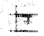
Fig. 5 extracts 1 of the pixel that is configured in the active matrix type display shown in Fig. 4 out and the plane graph that illustrates, and Fig. 6 (A), (B), (C) are respectively A-A ' profile, B-B ' profile and the C-C ' profiles of Fig. 5.
In the active matrix type display 1A of such structure, as shown in Fig. 5 and Fig. 6 (A), (B), in any pixel 7, all in same operation, utilize the semiconductor film of island to form 1TFT20 and 2TFT30.The gate electrode 21 of 1TFT20 is as the part of scan line gate and constitute.Be connected to the contact hole conductivity of data wire sig by the 1st interlayer dielectric 51 on the side of source-drain area of 1TFT20, be connected on its opposing party to drain electrode 22 conductivity.Drain electrode 22 extends towards the formation of 2TFT30 zone, is connected on this extension to the contact hole conductivity of the gate electrode 31 of 2TFT30 by the 1st interlayer dielectric 51.Be connected to the contact hole conductivity of repeater electrode 35 by the 1st interlayer dielectric 51 on the side of source-drain area of 2TFT30, be connected on this repeater electrode 35 to the contact hole conductivity of the pixel capacitors 41 of thin-film luminous element 40 by the 2nd interlayer dielectric 52.
From Fig. 5 and Fig. 6 (B), (C), as can be known, in each pixel 7, formed pixel capacitors 41 independently.In the upper layer side of pixel capacitors 41, by following sequential cascade organic semiconductor film 43 and opposite electrode op.Opposite electrode op formed cover display part 11 at least.
Have again, in Fig. 5 and Fig. 6 (A), be connected to the contact hole conductivity of common supply lines com by the 1st interlayer dielectric 51 on the opposing party of source-drain area of 2TFT30.The extension 39 of common supply lines com is with respect to the extension 36 of the gate electrode 31 of 2TFT30, the 1st interlayer dielectric 51 clamped as dielectric film and opposed, constituted maintenance electric capacity cap.
In such active matrix type display 1A since on transparency carrier 10 itself stacked opposite electrode op, so different with active array type LCD, have and there is no need the so big advantage of overlapping counter substrate.But, because the opposite electrode op that 40 quilts of thin-film luminous element are thin covers,, moisture and oxygen invades in the organic semiconductor film 43 worry of the decline of the luminous efficiency of existence generation thin-film luminous element 40, the rising (threshold voltage moves to high voltage one lateral deviation) of its driving voltage, reliability decrease etc. so spreading and see through opposite electrode op.In order to prevent the intrusion of above-mentioned moisture and oxygen, in existing active matrix type display 1A, adopted the method that covers display part 11 at least and the periphery of this counter substrate is sealed with counter substrate.But, use this method just to lose the advantage of comparing with above-mentioned liquid crystal indicator.
Therefore, problem of the present invention is to provide the active matrix type display that can come the protective film light-emitting component to make it not influenced by moisture etc. with simple structure.
Disclosure of an invention
Active matrix type display of the present invention has following structure.
On substrate, has the multi-strip scanning line; many data wires that intersect with this scan line and by being formed the display part that rectangular a plurality of pixels constitute by this data wire and above-mentioned scan line; each of this pixel possesses thin-film luminous element; this thin-film luminous element possesses and comprises the turn-on control circuit of accepting the thin-film transistor of sweep signal by above-mentioned scan line on gate electrode; the pixel capacitors that in each pixel, forms; at stacked light-emitting film of the upper layer side of this pixel capacitors and the opposite electrode that forms on whole at above-mentioned display part at least in the upper layer side of this light-emitting film; and luminous, this active matrix type display is characterised in that above-mentioned thin-film luminous element: the diaphragm that has formed the formation zone that covers this opposite electrode at least in the upper layer side of above-mentioned opposite electrode based on the picture intelligence that is supplied to from above-mentioned data wire by above-mentioned turn-on control circuit.
According to this structure owing to formed diaphragm in the upper layer side of the opposite electrode of thin-film luminous element, so can the protective film light-emitting component make its do not spread, through the influence of moisture of opposite electrode etc.Thereby, the worry of the decline of its luminous efficiency, the rising of driving voltage (threshold voltage moves to high voltage one lateral deviation), reliability decrease etc. does not take place in thin-film luminous element.In addition, owing to can utilize semiconductor technology easily to form such diaphragm, so can not improve the manufacturing cost of active matrix type display.Therefore, can in statu quo keep as the advantage of the active matrix type display that has used thin-film luminous element there is no need cover the such advantage of counter substrate, can improve the reliability of active matrix type display.Have again; owing to come the protective film light-emitting component with diaphragm; so also have following advantage: as the material that uses in the opposite electrode; consider to select this material to get final product from aspects such as the luminous efficiency of thin-film luminous element and driving voltages, be not limited to the high material of performance of selecting the protective film light-emitting component.
In the present invention, the dielectric film that preferably forms thickly by the lower layer side at above-mentioned opposite electrode than above-mentioned organic semiconductor film is divided above-mentioned light-emitting film.In the active matrix type display that has used thin-film luminous element,, be in and the opposed state of data wire, so big electric capacity parasitizes on the data wire under original state because opposite electrode forms on whole of display part at least.And in the present invention, because thick dielectric film is got involved between data wire and the opposite electrode, so can prevent that electric capacity from parasitizing on the data wire.Its result owing to can reduce the load of data side drive circuit, can seek the high speed of low power consumption or demonstration work.In addition, if form such dielectric film, then when utilizing formation light-emitting film in the zone that gunite divided by this dielectric film, above-mentioned dielectric film can be utilized as preventing to spray the dike layer that hydrorrhea goes out.
In the present invention, above-mentioned opposite electrode preferably constitutes by containing alkali-metal aluminium film.Constituting under the situation of opposite electrode with such film, because diffusions such as moisture, the possibility height that sees through are significant so form the effect of diaphragm.
In the present invention, can constitute said protection film with the dielectric film of silicon nitride film etc., but also can constitute by the conducting film of refractory metal or its alloy etc.In addition, also can constitute said protection film by pure aluminium film, the aluminium film that contains silicon, the conducting film that contains the aluminium film etc. of copper.Have again, also said protection film can be made 2 layers of structure of conducting film and dielectric film.Be stacked in the conducting film cambium layer under the situation of the diaphragm on the opposite electrode, can obtaining and make the same effect of resistance decline of opposite electrode.In addition; under the situation of the thick dielectric film that has formed the formation zone of dividing above-mentioned organic semiconductor film; the worry that fracture takes place in the opposite electrode that layer side forms is looked in existence thereon because of this film formed big step that insulate; but be stacked in the conducting film cambium layer under the situation of the diaphragm on the opposite electrode; owing to utilize such conducting film to form redundant wire structures, so can prevent the fracture of opposite electrode.Therefore, in active matrix type display, thereby even suppressed parasitic capacitance etc. owing to the periphery at organic semiconductor film forms thick dielectric film, in the opposite electrode that the upper strata of dielectric film forms, do not rupture, so can improve the display quality and the reliability of active matrix type display yet.
In the present invention, above-mentioned turn-on control circuit possesses at the 1TFT that accepts said scanning signals on the gate electrode with by this its gate electrode of 1TFT and is connected to 2TFT on the above-mentioned data wire, and it is that the drive current that constitutes is in addition supplied with between the common supply lines and above-mentioned opposite electrode of usefulness that this 2TFT and above-mentioned thin-film luminous element preferably are connected above-mentioned data wire and scan line with series system.That is, though available 1 TFT constitutes turn-on control circuit with maintenance electric capacity, from improving the viewpoint that shows grade, the most handy 2 TFT and maintenance electric capacity constitute the turn-on control circuit of each pixel.
The simple declaration of accompanying drawing
Fig. 1 is the schematically illustrated block diagram of having used the integral layout of active matrix type display of the present invention.
Fig. 2 extracts 1 of the pixel that is configured in the active matrix type display shown in Fig. 1 out and the plane graph that illustrates.
Fig. 3 (A), (B), (C) are respectively A-A ' profile, B-B ' profile and the C-C ' profiles of Fig. 2.
Fig. 4 is the block diagram of the integral layout of schematically illustrated existing active matrix type display.
Fig. 5 extracts 1 of the pixel that is configured in the active matrix type display shown in Fig. 4 out and the plane graph that illustrates.
Fig. 6 (A), (B), (C) are respectively A-A ' profile, B-B ' profile and the C-C ' profiles of Fig. 5.
The explanation of symbol
1 active matrix type display
2 display parts
3 data side drive circuits
4 scan-side drive circuits
7 pixels
10 transparency carriers
12 terminals
20 1TFT
The gate electrode of 21 1TFT
30 2TFT
The gate electrode of 31 2TFT
40 light-emitting components
41 pixel capacitors
43 organic semiconductors
60 diaphragms
Bank dike layer (dielectric film)
Cap keeps electric capacity
The common supply lines of com
The gate scan line
The op opposite electrode
The sig data wire
The optimal morphology that is used to carry out an invention
With reference to description of drawings example of the present invention.Have again, in the following description, for the common part of key element that has illustrated with reference to Fig. 4 to Fig. 6, attached with identical symbol.
(overall structure)
Fig. 1 is the block diagram of the integral layout of schematically illustrated active matrix type display.Fig. 2 extracts 1 of the pixel that wherein is configured out and the plane graph that illustrates, and Fig. 3 (A), (B), (C) are respectively A-A ' profile, B-B ' profile and the C-C ' profiles of Fig. 2.
In the active matrix type display 1 shown in Figure 1, become display part 11 as the middle body of the transparency carrier 10 of its matrix.In the outer peripheral portion of transparency carrier 10, constituted the data side drive circuit 3 of output image signal in the end of data wire sig, constituted the scan-side drive circuit 4 of output scanning signal in the end of scan line gate.In these drive circuits 3,4, constitute complementary type TFT by the TFT of N type and the TFT of P type, this complementary type TFT has constituted shift-register circuit, level shift circuit, analog switching circuit etc.In display part 11, identical with the active-matrix substrate of active array type LCD, constituted on transparency carrier 10 that upwardly extending many data wire sig form rectangular a plurality of pixels 7 by multi-strip scanning line gate with in the side that the bearing of trend with this scan line gate intersects.
In pixel 7 separately, constituted by scan line gate and be supplied to the turn-on control circuit 50 of sweep signal and based on the picture intelligence that is supplied to from data wire sig by this turn-on control circuit 50 and luminous thin-film luminous element 40.In the example shown here, turn-on control circuit 50 by the 1TFT20 that on gate electrode, accepts sweep signal by scan line gate, keep the maintenance electric capacity cap of the picture intelligence that is supplied to from data wire sig by this 1TFT20 and accept to constitute by the 2TFT30 of the picture intelligence of this maintenances electric capacity cap maintenance at gate electrode.2TFT30 and thin-film luminous element 40 are connected between the opposite electrode op and common supply lines com that below will at length narrate with series system.
In the active matrix type display 1 of such structure, as shown in Fig. 2 and Fig. 3 (A), (B), in which pixel 7, all utilize the semiconductor film (silicon fiml) of island to form 1TFT20 and 2TFT30.
The gate electrode 21 of 1TFT20 is as the part of scan line gate and constitute.Be connected to the contact hole conductivity of data wire sig by the 1st interlayer dielectric 51 on the side of source-drain area of 1TFT20, be connected on its opposing party to drain electrode 22 conductivity.Drain electrode 22 extends towards the formation of 2TFT30 zone, is connected on this extension to the contact hole conductivity of the gate electrode 31 of 2TFT30 by the 1st interlayer dielectric 51.
Be connected to the contact hole conductivity of the repeater electrode 35 that forms simultaneously with data wire sig by the 1st interlayer dielectric 51 on the side of source-drain area of 2TFT30, be connected on this repeater electrode 35 to the contact hole conductivity of the transparent pixel capacitors 41 that constitutes by the ITO film of thin-film luminous element 40 by the 2nd interlayer dielectric 52.
From Fig. 2 and Fig. 3 (B), (C), as can be known, in each pixel 7, formed pixel capacitors 41 independently.In the upper layer side of pixel capacitors 41, by following sequential cascade by the organic semiconductor film 43 of polyphenylene vinylene formations such as (PPV) with by the opposite electrode op that metal films such as alkali-metal aluminium, calcium such as containing lithium constitute, constituted thin-film luminous element 40.Though in each pixel 7, formed organic semiconductor film 43, also crossed a plurality of pixels 7 sometimes and form it into strip.Opposite electrode op in display part 11 integral body and except formed at least terminal 12 parts around the zone in form.
Have again, as thin-film luminous element 40, also can adopt the structure that is provided with hole injection layer and improves luminous efficiency (hole injection rate), be provided with structure that electron injecting layer improves luminous efficiency (electronics injection rate), formed the two structure of hole injection layer and electron injecting layer.
Have again, in Fig. 2 and Fig. 3 (A), be connected to the contact hole conductivity of common supply lines com by the 1st interlayer dielectric 51 on the opposing party of source-drain area of 2TFT30.The extension 39 of common supply lines com is with respect to the extension 36 of the gate electrode 31 of 2TFT30, the 1st interlayer dielectric 51 clamped as dielectric film and opposed, constituted maintenance electric capacity cap.
In the active matrix type display 1 that constitutes by this way, become conducting state if be scanned the 1TFT20 of signal selection, then will be applied to by 1TFT20 from the picture intelligence of data wire sig on the gate electrode 31 of 2TFT30, picture intelligence is written to by 1TFT20 and keeps among the electric capacity cap simultaneously.Its result, if 2TFT30 becomes conducting state, then respectively opposite electrode op and pixel capacitors 41 are applied voltage as negative pole and positive pole, applying voltage above in the zone of threshold voltage, the electric current (drive current) that flows through organic semiconductor film 43 sharply increases.Thereby and luminous, the light of light-emitting component 40 is reflected by opposite electrode op light-emitting component 40 as electroluminescent cell or LED element, sees through transparent pixel capacitors 41 and transparency carrier 10 and penetrates.Flow through the current path that constitutes by opposite electrode op, organic semiconductor film 43, pixel capacitors 41,2TFT30 and common supply lines com owing to carry out the drive current of such illuminating, so if 2TFT30 becomes off state, then electric current does not flow.But even because 1TFT20 becomes off state, the gate electrode of 2TFT30 is also owing to keeping electric capacity cap to remain in the current potential suitable with picture intelligence, so 2TFT30 still is in original conducting state.Therefore, drive current continues to flow through light-emitting component 40, and this pixel still is in original illuminating state.This state be maintained to new pictorial data is written to keep among the electric capacity cap, 2TFT30 becomes till the off state.
(the protection structure of thin-film luminous element)
Like this, in the active matrix type display 1 that has used thin-film luminous element 40, because stacked opposite electrode op on transparency carrier 10 itself, thus different with active array type LCD, have and there is no need the so big advantage of overlapping counter substrate.But, have the diffusion of moisture and oxygen and see through thin opposite electrode op to invade worry in the thin-film luminous element 40.Particularly in this form, to improve the electron injection efficiency in the thin-film luminous element 40 and to reduce its driving voltage is purpose, uses alkali-metal aluminium films such as containing lithium as opposite electrode op, it is generally acknowledged, this contains alkali-metal aluminium film compares with pure aluminium film, spreads easily and sees through moisture and oxygen.That is because contain alkali-metal aluminium film and pure aluminium film, contain the aluminium film of silicon, the aluminium film that contains copper is compared lacking toughness, when stress application, rupture easily, so there is moisture and oxygen worry by intrusions such as crackles.In addition, the plane of disruption that contains alkali-metal aluminium film demonstrates columnar structure, it is generally acknowledged the easily diffusion and seeing through between tissue of moisture and oxygen.
Therefore, in this form, formed the diaphragm 60 that constitutes by fine aluminium on the upper strata of opposite electrode op.Because the diaphragm 60 that should be made of fine aluminium have the toughness that does not rupture under the situation of stress more or less, so do not become the crackle in moisture and oxygen intrusion path.In addition, in the plane of disruption of fine aluminium, do not demonstrate and contain the such columnar structure of alkali-metal aluminium film, so do not have moisture and oxygen to see through, invade the worry between tissue yet.Therefore; because the active matrix type display 1 of this form can protective film light-emitting component 40 be subjected to the influence of moisture etc., so the decline of luminous efficiency, the rising of driving voltage (threshold voltage moves to high voltage one lateral deviation), reliability decrease etc. do not take place in thin-film luminous element 40.In addition, if the diaphragm 60 that constitutes by such pure aluminium film, then owing to can utilize semiconductor technology easily to form, so can not improve the manufacturing cost of active matrix type display 1.Therefore, can in statu quo keep as the advantage of the active matrix type display 1 that has used thin-film luminous element 40 there is no need cover the such advantage of counter substrate, can improve the reliability of active matrix type display 1.
Have again; owing to come protective film light-emitting component 40 with diaphragm 60; so also have following advantage: as the material that uses among the opposite electrode op; consider to select this material to get final product from aspects such as the luminous efficiency of thin-film luminous element 40 and driving voltages, be not limited to the high material of performance of selecting protective film light-emitting component 40.
Have again, in this form,, can obtain and make the same effect of resistance decline of opposite electrode op owing to use the conducting film cambium layer that constitutes by pure aluminium film to be stacked in diaphragm 60 on the opposite electrode op
(structure of dike layer)
In the active matrix type display 1 that constitutes by this way, in this form, in order to prevent that big electric capacity from parasitizing on the data wire sig, as shown in Fig. 1, Fig. 2 and Fig. 3 (A), (B), (C), along data wire sig and scan line gate, be provided with the thick dielectric film that constitutes by resist film or polyimide film (dike layer bank/ added with wide spacing towards the lower left to the zone of oblique line), formed opposite electrode op in the upper layer side of this dike layer bank.Therefore, owing between data wire sig and opposite electrode op, get involved the 2nd interlayer dielectric 52 and thick dike layer bank, so the electric capacity that parasitizes on the data wire sig is minimum.Therefore, the load of drive circuit 3,4 can be reduced, the high speed of low power consumption or demonstration work can be sought.
In addition, as shown in fig. 1, in the neighboring area of transparency carrier 10 (exterior lateral area of display part 11), also formed dike layer bank (attached with oblique line in forming the zone).Thereby data side drive circuit 3 and scan-side drive circuit 4 are all covered by dike layer bank.Opposite electrode op forms in display part 11 at least, but there is no need to form in the formation zone of drive circuit.But because opposite electrode op forms with the mask sputtering method usually, so alignment precision is relatively poor, opposite electrode op and drive circuit are overlapping sometimes.Like this,, between the wiring layer of drive circuit and opposite electrode op, also got involved dike layer bank, parasitized on the drive circuit 3,4 so can prevent electric capacity even because the formation zone of opposite electrode op and drive circuit is in overlap condition.Therefore, the load of drive circuit 3,4 can be reduced, the high speed of low power consumption or demonstration work can be sought.
Have again, in this form, in the formation zone of pixel capacitors 41, dike layer bank also with repeater electrode 35 overlapping areas of turn-on control circuit 50 in form.Therefore, with repeater electrode 35 overlapping areas in do not form organic semiconductor film 43.That is,,, can not cause the irregular of demonstration so form organic semiconductor film 43 with constant thickness owing to form on 43 flat portions in the formation zone of pixel capacitors 41 of organic semiconductor film.In addition, if with repeater electrode 35 overlapping areas in do not have dike layer bank, even then in this part drive current flow through and opposite electrode op between, organic semiconductor film 43 is also luminous.But this light is sandwiched between repeater electrode 35 and the opposite electrode op, does not outwards penetrate, to showing not contribution.From showing this respect, can be described as idle current at such drive current that demonstration is not had flow in the part of contribution.And in this form,, prevent that drive current from flowing at this place, flows through common supply lines com so can prevent useless electric current owing in the part that should flow through such idle current up to now, form dike layer bank.Therefore, the width of common supply lines com correspondingly can narrow down.As its result, can increase light-emitting area, can improve the display performance of brightness, contrast etc.
At this, under the situation that has formed thick dike layer bank, as shown in Figure 3, exist the big step difference bb that forms because of dike layer bank that the worry of fracture takes place in the opposite electrode op that layer side forms thereon.And in this form, owing to the diaphragm 60 that is stacked in the conducting film cambium layer on the opposite electrode op, so constituted redundant wire structures by such conducting film (diaphragm 60).Thereby, even thereby forming thick dike layer bank has suppressed parasitic capacitance etc., in the opposite electrode op that the upper strata of dike layer bank forms, do not rupture, so can improve the display quality and the reliability of active matrix type display 1 yet.
Have, if form dike layer bank with the resist of black, then dike layer bank plays the function as black matrix" again, improved the grade of demonstrations such as contrast.That is, in the active matrix type display relevant 1, because opposite electrode op forms on the surface of transparency carrier 10 side whole at pixel 7, so the reverberation at opposite electrode op place makes contrast decline with this form.And if constitute the dike layer bank that takes on the function that prevents parasitic capacitance with the resist of black, then because dike layer bank also plays function as black matrix", cover reverberation, so can improve contrast from opposite electrode op.
(manufacture method of active matrix type display)
Because the dike layer bank that forms constitutes in the mode in the formation zone of encirclement organic semiconductor film 43 by this way, so in the manufacturing process of active matrix type display, stop ejection liquid when forming organic semiconductor film 43 to prevent that spraying liquid overflows to the side at aqueous material (ejection liquid) by the injector head ejection.Have again, in the manufacture method of the active matrix type display 1 of following explanation, since roughly the same to the operation till making 1TFT20 and 2TFT30 on the transparency carrier 10 with the operation of the active-matrix substrate of making active array type LCD 1, so its summary is described simply with reference to Fig. 3 (A), (B), (C).
At first; for transparency carrier 10; as required; with TEOS (tetraethyl oxosilane) or oxygen etc. as unstrpped gas; utilize plasma CVD method to form and be about the base protective film (not shown) that the silicon oxide film of 2000~5000 dusts constitutes, utilize plasma CVD method on the surface of base protective film, to form afterwards and be about the semiconductor film that amorphous silicon fiml of 300~700 dusts constitutes by thickness by thickness.Secondly, the semiconductor film that is made of amorphous silicon fiml is carried out crystallization step such as laser annealing or solid state growth method, make the semiconductor film crystallization become polysilicon film.
Secondly, semiconductor film is carried out pattern etching, make the semiconductor film of island, TEOS (tetraethyl oxosilane) or oxygen etc. as unstrpped gas, are utilized plasma CVD method to form in its surface by thickness and are about the silicon oxide film of 600~1500 dusts or the gate insulating film 57 that nitride film constitutes.
Secondly, utilize sputtering method to form the conducting film that the metal film by aluminium, tantalum, molybdenum, titanium, tungsten etc. constitutes, carry out pattern etching afterwards, form the extension 36 (gate electrode formation operation) of gate electrode 21,31 and gate electrode 31.In this operation, also form scan line gate.
Under this state, inject the phosphonium ion of high concentration, form source-drain area with respect to gate electrode 21,31 in self aligned mode.Have, the part that does not import impurity becomes channel region again.
Secondly, after having formed the 1st interlayer dielectric 51, form each contact hole, secondly, form extension 39 and the repeater electrode 35 of data wire sig, drain electrode 22, common supply lines com, common supply lines com.Its result forms 1TFT20,2TFT30 and keeps electric capacity cap.
Secondly, form the 2nd interlayer dielectric 52, in this interlayer dielectric, form contact hole at the part place suitable with repeater electrode 35.Secondly, on the whole surface of the 2nd interlayer dielectric 52, formed the ITO film after, carry out pattern etching, the pixel capacitors 41 that is connected with in each pixel 7, forming source-drain area conductivity by contact hole and 2TFT30.
Secondly, a side has formed resist layer on the surface of the 2nd interlayer dielectric 52, carries out pattern etching afterwards so that stay this resist along scan line gate and data wire sig, forms dike layer bank.At this moment, make the resist wider width partly that stays along data wire sig, so that cover common supply lines com.Its result, the zone that should form the organic semiconductor film 43 of light-emitting component 40 is surrounded by dike layer bank.Secondly, utilize gunite be divided into rectangular zone by dike layer bank in formation corresponding to each organic semiconductor film 43 of R, G, B.For this reason, with respect to the medial region of dike layer bank, the aqueous material (precursor) from injector head ejection formation organic semiconductor film 43 usefulness is fixed in the medial region of dike layer bank, forms organic semiconductor film 43.At this, owing to dike layer bank is made of resist, so be hydrophobicity.Different therewith, because the precursor of organic semiconductor film 43 uses hydrophilic solvent,, can not spill in the pixel 7 of adjacency so the area of application of organic semiconductor film 43 is definite reliably by dike layer bank.Therefore, can only in predetermined zone, form organic semiconductor film 43 etc.In this operation, from the precursor of injector head ejection because the thickness of about 2 μ m to about 4 μ m is heaved in capillary influence, so the thickness of dike layer bank must be extremely about 3 μ m of about 1 μ m.Have, the thickness of the organic semiconductor film 43 after fixing is that about 0.05 μ m is to about 0.2 μ m again.Have, if the height in the next door that is made of dike layer bank is more than the 1 μ m, even dike layer bank is not hydrophobicity, dike layer bank also can fully play the effect as the next door again.If be pre-formed so thick dike layer bank, even then can determine that also this formations is regional using coating process to replace gunite to form under the situation of organic semiconductor film 43.
On roughly whole of transparency carrier 10 form opposite electrode op, again at the upper strata of opposite electrode op stacked guard film 60 thereafter.If the thickness of diaphragm 60 is about 2000 dusts~1 μ m, then can guarantee enough moisture-proofs.
According to such manufacture method, owing to can utilize gunite in predetermined zone, to form each organic semiconductor film 43 corresponding to R, G, B, so can be with the active matrix type display 1 of high productivity ratio manufacturing full color.
Have again, also form TFT in data side drive circuit 3 shown in Figure 1 and the scan-side drive circuit 4, but these TFT utilize the operation that in above-mentioned pixel 7, forms TFT all or part of form.Therefore, the TFT of formation drive circuit forms at the interlayer identical with the TFT of pixel 7.In addition, about above-mentioned 1TFT20 and 2TFT30, both are N types, both are P types, the one, and another person of N type is that any of the such situation of P type all is fine, even but because the combination of such any, also can utilize well-known method to form TFT, its explanation of Therefore, omited.
[other example]
Have again, as diaphragm 60, to form with the same method of the above embodiments, except pure aluminium film, if moisture and oxygen see through few conducting film, the metal film of the aluminium film that then can use the aluminium film that contains silicon, contains copper or other metal.In addition, as diaphragm 60, can use refractory metal or its alloy.Have again, using under the situation of dielectric film as diaphragm 60 of silicon nitride film etc., also can prevent the performance depreciation of thin-film luminous element 40.Moreover, also diaphragm 60 can be made this two-layer structure of dielectric film and conducting film, in this case,, then can realize above-mentioned redundant wire structures if for the stacked conducting film of opposite electrode op.Under any situation,, then all can guarantee enough moisture-proofs if the thickness of diaphragm is about 2000 dusts~1 μ m.
In addition, about dike layer bank (dielectric film), under the situation that the organic material by resist film, polyimide film etc. constitutes, can easily form thick film, but constituting under the situation of dike layer bank dielectric film by inorganic material with the silicon oxide film of CVD method or SOG method film forming or silicon nitride film etc., even be in organic semiconductor film 43 state of contact under, also can prevent the rotten of organic semiconductor film 43.
In addition, about keeping electric capacity cap, except and common supply lines com between the structure that forms, also can and the electric capacity line that forms side by side of scan line gate between form, in addition, also can be the structure of having utilized the gate electrode 31 of the drain region of 1TFT20 and 2TFT30.
As discussed above, in the active matrix type display relevant, owing to formed diaphragm, so energy protective film light-emitting component makes it not influenced by moisture etc. in the upper layer side of the opposite electrode of thin-film luminous element with the present invention.Thereby, there is not the worry of thin-film luminous element performance depreciation.In addition, owing to can utilize semiconductor technology easily to form such diaphragm, so can not improve the manufacturing cost of active matrix type display.Therefore, can in statu quo keep as the advantage of the active matrix type display that has used thin-film luminous element there is no need cover the such advantage of counter substrate, can improve the reliability of active matrix type display.Have again; owing to come the protective film light-emitting component with diaphragm; so also have following advantage: as the material that uses in the opposite electrode; consider to select this material to get final product from aspects such as the luminous efficiency of thin-film luminous element and driving voltages, be not limited to the high material of performance of selecting the protective film light-emitting component.
Utilize possibility on the industry
Because the present invention has above-mentioned effect, so be suitable for sending out as by thin film transistor (TFT) the field being caused The thin-film luminous element of optical element or light-emitting diode etc. drives the active array type of control Display unit is used. In addition, having used active matrix type display of the present invention can not only use In personal computer, portable information terminal, also can be widely used in outdoor large-scale telegraph board, The information display device of billboard etc.
Claims (15)
1. display unit comprises:
The multi-strip scanning line;
Many data wires;
Drive circuit, described drive circuit are connected to described multi-strip scanning line or described multi-strip scanning line; With
Display part, described display part comprise a plurality of pixels that the joining of described multi-strip scanning line and described many data wires limits and forms, and each pixel in described a plurality of pixels comprises:
Turn-on control circuit, described turn-on control circuit comprises the first transistor, sweep signal offers the grid of described the first transistor by a corresponding scan line in the described multi-strip scanning line, offers described turn-on control circuit from the picture signal of a corresponding data wire in described many data wires by described the first transistor;
Pixel electrode; With
Light-emitting film, described light-emitting film between described pixel electrode and opposite electrode,
Described opposite electrode covers the part of described display part and overlapping at least described drive circuit at least,
Dielectric film, described dielectric film place between described drive circuit and the described opposite electrode and
Diaphragm, described diaphragm covers described opposite electrode.
2. the display unit described in claim 1 is characterized in that:
Divide described light-emitting film by the dielectric film that the lower layer side at described opposite electrode forms thickly than described light-emitting film.
3. the display unit described in claim 1 or 2 is characterized in that:
Described opposite electrode constitutes by containing alkali-metal aluminium film.
4. the display unit described in claim 1 or 2 is characterized in that:
Described diaphragm is made of dielectric film.
5. the display unit described in claim 3 is characterized in that:
Described diaphragm is made of dielectric film.
6. the display unit described in claim 1 or 2 is characterized in that:
Described diaphragm is made of silicon nitride film.
7. the display unit described in claim 3 is characterized in that:
Described diaphragm is made of silicon nitride film.
8. the display unit described in claim 1 or 2 is characterized in that:
Described diaphragm is made of refractory metal or its alloy.
9. the display unit described in claim 3 is characterized in that:
Described diaphragm is made of refractory metal or its alloy.
10. the display unit described in claim 1 or 2 is characterized in that:
Described diaphragm by pure aluminium film, contain the aluminium film of silicon and any aluminium film of containing in the aluminium film of copper constitutes.
11. the display unit described in claim 3 is characterized in that:
Described diaphragm by pure aluminium film, contain the aluminium film of silicon and any aluminium film of containing in the aluminium film of copper constitutes.
12. the display unit described in claim 1 or 2 is characterized in that:
Described diaphragm becomes 2 layers of structure of conducting film and dielectric film.
13. the display unit described in claim 3 is characterized in that:
Described diaphragm becomes 2 layers of structure of conducting film and dielectric film.
14. the display unit described in claim 1 is characterized in that also comprising:
Many common supply lines,
Described turn-on control circuit also comprises transistor seconds, the grid of described transistor seconds is connected to a corresponding data wire in the described data wire by described the first transistor, and described transistor seconds places between the corresponding common supply lines and described pixel electrode of described many common supply lines.
15. the display unit described in claim 1 is characterized in that:
Described diaphragm comprises double-decker.
Applications Claiming Priority (2)
| Application Number | Priority Date | Filing Date | Title |
|---|---|---|---|
| JP23492197A JP3830238B2 (en) | 1997-08-29 | 1997-08-29 | Active matrix type device |
| JP234921/1997 | 1997-08-29 |
Related Child Applications (1)
| Application Number | Title | Priority Date | Filing Date |
|---|---|---|---|
| CNB031406548A Division CN1278292C (en) | 1997-08-29 | 1998-08-25 | Active matrix display device |
Publications (2)
| Publication Number | Publication Date |
|---|---|
| CN1242924A CN1242924A (en) | 2000-01-26 |
| CN1138457C true CN1138457C (en) | 2004-02-11 |
Family
ID=16978379
Family Applications (2)
| Application Number | Title | Priority Date | Filing Date |
|---|---|---|---|
| CNB031406548A Expired - Lifetime CN1278292C (en) | 1997-08-29 | 1998-08-25 | Active matrix display device |
| CNB988015846A Expired - Lifetime CN1138457C (en) | 1997-08-29 | 1998-08-25 | Active matrix display |
Family Applications Before (1)
| Application Number | Title | Priority Date | Filing Date |
|---|---|---|---|
| CNB031406548A Expired - Lifetime CN1278292C (en) | 1997-08-29 | 1998-08-25 | Active matrix display device |
Country Status (8)
| Country | Link |
|---|---|
| US (2) | US6359606B1 (en) |
| EP (1) | EP0961525B1 (en) |
| JP (1) | JP3830238B2 (en) |
| KR (1) | KR100483225B1 (en) |
| CN (2) | CN1278292C (en) |
| DE (1) | DE69824392T2 (en) |
| TW (1) | TW426841B (en) |
| WO (1) | WO1999012394A1 (en) |
Families Citing this family (157)
| Publication number | Priority date | Publication date | Assignee | Title |
|---|---|---|---|---|
| US6462722B1 (en) | 1997-02-17 | 2002-10-08 | Seiko Epson Corporation | Current-driven light-emitting display apparatus and method of producing the same |
| CN100341042C (en) | 1997-02-17 | 2007-10-03 | 精工爱普生株式会社 | Display device |
| JP3520396B2 (en) * | 1997-07-02 | 2004-04-19 | セイコーエプソン株式会社 | Active matrix substrate and display device |
| JP3580092B2 (en) * | 1997-08-21 | 2004-10-20 | セイコーエプソン株式会社 | Active matrix display |
| CN1267871C (en) * | 1997-08-21 | 2006-08-02 | 精工爱普生株式会社 | Display device |
| JP3830238B2 (en) * | 1997-08-29 | 2006-10-04 | セイコーエプソン株式会社 | Active matrix type device |
| US6492769B1 (en) * | 1998-12-25 | 2002-12-10 | Canon Kabushiki Kaisha | Electron emitting device, electron source, image forming apparatus and producing methods of them |
| US7821065B2 (en) | 1999-03-02 | 2010-10-26 | Semiconductor Energy Laboratory Co., Ltd. | Semiconductor device comprising a thin film transistor comprising a semiconductor thin film and method of manufacturing the same |
| TW444257B (en) * | 1999-04-12 | 2001-07-01 | Semiconductor Energy Lab | Semiconductor device and method for fabricating the same |
| US6512504B1 (en) | 1999-04-27 | 2003-01-28 | Semiconductor Energy Laborayory Co., Ltd. | Electronic device and electronic apparatus |
| US8853696B1 (en) | 1999-06-04 | 2014-10-07 | Semiconductor Energy Laboratory Co., Ltd. | Electro-optical device and electronic device |
| JP4515349B2 (en) * | 1999-06-04 | 2010-07-28 | 株式会社半導体エネルギー研究所 | Electro-optic device |
| US7288420B1 (en) * | 1999-06-04 | 2007-10-30 | Semiconductor Energy Laboratory Co., Ltd. | Method for manufacturing an electro-optical device |
| TWI232595B (en) * | 1999-06-04 | 2005-05-11 | Semiconductor Energy Lab | Electroluminescence display device and electronic device |
| JP4094437B2 (en) * | 1999-06-04 | 2008-06-04 | 株式会社半導体エネルギー研究所 | Method for manufacturing electro-optical device |
| JP4515469B2 (en) * | 1999-06-04 | 2010-07-28 | 株式会社半導体エネルギー研究所 | Method for manufacturing electro-optical device |
| JP4730994B2 (en) * | 1999-06-04 | 2011-07-20 | 株式会社半導体エネルギー研究所 | Electro-optical device, manufacturing method thereof, and electronic device |
| JP4532452B2 (en) * | 1999-06-04 | 2010-08-25 | 株式会社半導体エネルギー研究所 | Electro-optic device |
| JP4532453B2 (en) * | 1999-06-04 | 2010-08-25 | 株式会社半導体エネルギー研究所 | Method for manufacturing electro-optical device |
| TW556357B (en) * | 1999-06-28 | 2003-10-01 | Semiconductor Energy Lab | Method of manufacturing an electro-optical device |
| JP4497596B2 (en) * | 1999-09-30 | 2010-07-07 | 三洋電機株式会社 | Thin film transistor and display device |
| JP2001109395A (en) * | 1999-10-01 | 2001-04-20 | Sanyo Electric Co Ltd | El display device |
| JP2001109405A (en) * | 1999-10-01 | 2001-04-20 | Sanyo Electric Co Ltd | El display device |
| JP2001102169A (en) | 1999-10-01 | 2001-04-13 | Sanyo Electric Co Ltd | El display |
| TW480722B (en) | 1999-10-12 | 2002-03-21 | Semiconductor Energy Lab | Manufacturing method of electro-optical device |
| JP4780826B2 (en) * | 1999-10-12 | 2011-09-28 | 株式会社半導体エネルギー研究所 | Method for manufacturing electro-optical device |
| TW535454B (en) * | 1999-10-21 | 2003-06-01 | Semiconductor Energy Lab | Electro-optical device |
| US6587086B1 (en) * | 1999-10-26 | 2003-07-01 | Semiconductor Energy Laboratory Co., Ltd. | Electro-optical device |
| JP2001126867A (en) * | 1999-10-26 | 2001-05-11 | Seiko Epson Corp | Method of manufacturing display |
| US6580094B1 (en) * | 1999-10-29 | 2003-06-17 | Semiconductor Energy Laboratory Co., Ltd. | Electro luminescence display device |
| JP2001195016A (en) * | 1999-10-29 | 2001-07-19 | Semiconductor Energy Lab Co Ltd | Electronic device |
| JP4906145B2 (en) * | 1999-11-29 | 2012-03-28 | 株式会社半導体エネルギー研究所 | EL display device |
| KR20010103000A (en) * | 1999-11-29 | 2001-11-17 | 요트.게.아. 롤페즈 | Organic electroluminescent device and a method of manufacturing thereof |
| JP2001175198A (en) | 1999-12-14 | 2001-06-29 | Semiconductor Energy Lab Co Ltd | Semiconductor device and manufacturing method therefor |
| TWI252592B (en) * | 2000-01-17 | 2006-04-01 | Semiconductor Energy Lab | EL display device |
| JP2001230077A (en) * | 2000-02-18 | 2001-08-24 | Dainippon Printing Co Ltd | Manufacturing method of electroluminescence element |
| TW525305B (en) * | 2000-02-22 | 2003-03-21 | Semiconductor Energy Lab | Self-light-emitting device and method of manufacturing the same |
| JP4831873B2 (en) * | 2000-02-22 | 2011-12-07 | 株式会社半導体エネルギー研究所 | Self-luminous device and manufacturing method thereof |
| US7129918B2 (en) * | 2000-03-10 | 2006-10-31 | Semiconductor Energy Laboratory Co., Ltd. | Electronic device and method of driving electronic device |
| US7301276B2 (en) * | 2000-03-27 | 2007-11-27 | Semiconductor Energy Laboratory Co., Ltd. | Light emitting apparatus and method of manufacturing the same |
| JP4618918B2 (en) * | 2000-03-27 | 2011-01-26 | 株式会社半導体エネルギー研究所 | Method for manufacturing self-luminous device |
| TW493282B (en) * | 2000-04-17 | 2002-07-01 | Semiconductor Energy Lab | Self-luminous device and electric machine using the same |
| JP4889872B2 (en) * | 2000-04-17 | 2012-03-07 | 株式会社半導体エネルギー研究所 | Light emitting device and electric appliance using the same |
| JP4713010B2 (en) * | 2000-05-08 | 2011-06-29 | 株式会社半導体エネルギー研究所 | Light emitting device and manufacturing method thereof |
| JP4860052B2 (en) * | 2000-05-12 | 2012-01-25 | 株式会社半導体エネルギー研究所 | Light emitting device |
| US8610645B2 (en) | 2000-05-12 | 2013-12-17 | Semiconductor Energy Laboratory Co., Ltd. | Display device |
| TW554637B (en) * | 2000-05-12 | 2003-09-21 | Semiconductor Energy Lab | Display device and light emitting device |
| US7339317B2 (en) * | 2000-06-05 | 2008-03-04 | Semiconductor Energy Laboratory Co., Ltd. | Light-emitting device having triplet and singlet compound in light-emitting layers |
| US7430025B2 (en) | 2000-08-23 | 2008-09-30 | Semiconductor Energy Laboratory Co., Ltd. | Portable electronic device |
| US6864628B2 (en) * | 2000-08-28 | 2005-03-08 | Semiconductor Energy Laboratory Co., Ltd. | Light emitting device comprising light-emitting layer having triplet compound and light-emitting layer having singlet compound |
| JP2002083691A (en) * | 2000-09-06 | 2002-03-22 | Sharp Corp | Active matrix driven organic led display unit and its manufacturing method |
| JP2002184569A (en) * | 2000-10-03 | 2002-06-28 | Semiconductor Energy Lab Co Ltd | Luminescent device |
| US6924594B2 (en) * | 2000-10-03 | 2005-08-02 | Semiconductor Energy Laboratory Co., Ltd. | Light emitting device |
| JP2005100992A (en) * | 2000-10-26 | 2005-04-14 | Semiconductor Energy Lab Co Ltd | Light-emitting device |
| US6664732B2 (en) | 2000-10-26 | 2003-12-16 | Semiconductor Energy Laboratory Co., Ltd. | Light emitting device and manufacturing method thereof |
| TW522577B (en) | 2000-11-10 | 2003-03-01 | Semiconductor Energy Lab | Light emitting device |
| JP4632337B2 (en) * | 2000-11-10 | 2011-02-16 | 株式会社半導体エネルギー研究所 | Light emitting device |
| US6893887B2 (en) * | 2001-01-18 | 2005-05-17 | Semiconductor Energy Laboratory Co., Ltd. | Process for producing a light emitting device |
| SG118110A1 (en) | 2001-02-01 | 2006-01-27 | Semiconductor Energy Lab | Organic light emitting element and display device using the element |
| JP4101529B2 (en) * | 2001-02-22 | 2008-06-18 | 株式会社半導体エネルギー研究所 | Display device and manufacturing method thereof |
| US6992439B2 (en) | 2001-02-22 | 2006-01-31 | Semiconductor Energy Laboratory Co., Ltd. | Display device with sealing structure for protecting organic light emitting element |
| JP3608614B2 (en) | 2001-03-28 | 2005-01-12 | 株式会社日立製作所 | Display device |
| JP4801278B2 (en) * | 2001-04-23 | 2011-10-26 | 株式会社半導体エネルギー研究所 | Light emitting device and manufacturing method thereof |
| US7294517B2 (en) * | 2001-06-18 | 2007-11-13 | Semiconductor Energy Laboratory Co., Ltd. | Light emitting device and method of fabricating the same |
| JP2003076301A (en) * | 2001-09-07 | 2003-03-14 | Matsushita Electric Ind Co Ltd | Light emitting element and display device using the element |
| JP4019690B2 (en) * | 2001-11-02 | 2007-12-12 | セイコーエプソン株式会社 | ELECTRO-OPTICAL DEVICE, MANUFACTURING METHOD THEREOF, AND ELECTRONIC DEVICE |
| US7483001B2 (en) | 2001-11-21 | 2009-01-27 | Seiko Epson Corporation | Active matrix substrate, electro-optical device, and electronic device |
| TWI250498B (en) * | 2001-12-07 | 2006-03-01 | Semiconductor Energy Lab | Display device and electric equipment using the same |
| CN1209662C (en) * | 2001-12-17 | 2005-07-06 | 精工爱普生株式会社 | Display device and electronic apparatus |
| JP4182467B2 (en) * | 2001-12-27 | 2008-11-19 | セイコーエプソン株式会社 | Circuit board, electro-optical device and electronic apparatus |
| KR100467943B1 (en) * | 2001-12-28 | 2005-01-24 | 엘지.필립스 엘시디 주식회사 | The organic electroluminescence device and method of fabricating the same |
| US7038377B2 (en) | 2002-01-16 | 2006-05-02 | Seiko Epson Corporation | Display device with a narrow frame |
| SG126714A1 (en) * | 2002-01-24 | 2006-11-29 | Semiconductor Energy Lab | Light emitting device and method of manufacturing the same |
| JP3818261B2 (en) | 2002-01-24 | 2006-09-06 | セイコーエプソン株式会社 | LIGHT EMITTING DEVICE AND ELECTRONIC DEVICE |
| TWI258317B (en) | 2002-01-25 | 2006-07-11 | Semiconductor Energy Lab | A display device and method for manufacturing thereof |
| JP4310984B2 (en) * | 2002-02-06 | 2009-08-12 | 株式会社日立製作所 | Organic light emitting display |
| EP1343206B1 (en) | 2002-03-07 | 2016-10-26 | Semiconductor Energy Laboratory Co., Ltd. | Light emitting apparatus, electronic apparatus, illuminating device and method of fabricating the light emitting apparatus |
| US6885146B2 (en) | 2002-03-14 | 2005-04-26 | Semiconductor Energy Laboratory Co., Ltd. | Display device comprising substrates, contrast medium and barrier layers between contrast medium and each of substrates |
| JP4197233B2 (en) * | 2002-03-20 | 2008-12-17 | 株式会社日立製作所 | Display device |
| CN101488481B (en) * | 2002-05-28 | 2011-05-11 | 精工爱普生株式会社 | Light-emitting device and electronic apparatus |
| JP3778176B2 (en) | 2002-05-28 | 2006-05-24 | セイコーエプソン株式会社 | LIGHT EMITTING DEVICE AND ELECTRONIC DEVICE |
| KR20030093016A (en) * | 2002-06-01 | 2003-12-06 | 삼성에스디아이 주식회사 | Organic electroluminescence device |
| JP4001066B2 (en) | 2002-07-18 | 2007-10-31 | セイコーエプソン株式会社 | Electro-optical device, wiring board, and electronic equipment |
| US7150537B2 (en) * | 2002-08-16 | 2006-12-19 | Infocus Corporation | Projection television device and screen |
| JP3729262B2 (en) | 2002-08-29 | 2005-12-21 | セイコーエプソン株式会社 | ELECTROLUMINESCENT DEVICE AND ELECTRONIC DEVICE |
| JP2004095482A (en) * | 2002-09-03 | 2004-03-25 | Chi Mei Electronics Corp | Image display device |
| JP3922374B2 (en) | 2002-09-25 | 2007-05-30 | セイコーエプソン株式会社 | Electro-optical device, matrix substrate, and electronic apparatus |
| JP3997888B2 (en) | 2002-10-25 | 2007-10-24 | セイコーエプソン株式会社 | Electro-optical device, method of manufacturing electro-optical device, and electronic apparatus |
| JP4042548B2 (en) * | 2002-11-29 | 2008-02-06 | セイコーエプソン株式会社 | Electro-optical device and electronic apparatus |
| KR100895313B1 (en) * | 2002-12-11 | 2009-05-07 | 삼성전자주식회사 | Organic electro-luminescence display panel |
| US7710019B2 (en) | 2002-12-11 | 2010-05-04 | Samsung Electronics Co., Ltd. | Organic light-emitting diode display comprising auxiliary electrodes |
| KR100521272B1 (en) * | 2002-12-20 | 2005-10-12 | 삼성에스디아이 주식회사 | OELD with improved brightness |
| KR20040055337A (en) * | 2002-12-20 | 2004-06-26 | 엘지.필립스 엘시디 주식회사 | Liquid Crystal Display and Driving Apparatus Thereof |
| KR100490625B1 (en) * | 2003-02-20 | 2005-05-17 | 삼성에스디아이 주식회사 | Image display apparatus |
| JP2004361424A (en) * | 2003-03-19 | 2004-12-24 | Semiconductor Energy Lab Co Ltd | Element substrate, light emitting device and driving method of light emitting device |
| JP2004304009A (en) * | 2003-03-31 | 2004-10-28 | Canon Inc | Organic thin film transistor |
| KR20050119685A (en) * | 2003-04-08 | 2005-12-21 | 코닌클리케 필립스 일렉트로닉스 엔.브이. | Two sided light emitting device |
| US7250720B2 (en) | 2003-04-25 | 2007-07-31 | Semiconductor Energy Laboratory Co., Ltd. | Display device |
| US7161184B2 (en) * | 2003-06-16 | 2007-01-09 | Semiconductor Energy Laboratory Co., Ltd. | Display device and method for manufacturing the same |
| US7221095B2 (en) | 2003-06-16 | 2007-05-22 | Semiconductor Energy Laboratory Co., Ltd. | Light emitting device and method for fabricating light emitting device |
| US7224118B2 (en) | 2003-06-17 | 2007-05-29 | Semiconductor Energy Laboratory Co., Ltd. | Display device and electronic apparatus having a wiring connected to a counter electrode via an opening portion in an insulating layer that surrounds a pixel electrode |
| US20040263072A1 (en) * | 2003-06-24 | 2004-12-30 | Joon-Young Park | Flat panel display |
| SG142140A1 (en) | 2003-06-27 | 2008-05-28 | Semiconductor Energy Lab | Display device and method of manufacturing thereof |
| KR20050005085A (en) * | 2003-07-01 | 2005-01-13 | 엘지전자 주식회사 | Organic electroluminescence device and fabricating method thereof |
| KR100544123B1 (en) * | 2003-07-29 | 2006-01-23 | 삼성에스디아이 주식회사 | Flat panel display |
| EP1511095A3 (en) * | 2003-08-19 | 2011-02-23 | LG Display Co., Ltd. | Organic electroluminescent device and method of manufacturing the same |
| KR100551046B1 (en) * | 2003-08-28 | 2006-02-09 | 삼성에스디아이 주식회사 | Organic EL device |
| CN100411186C (en) * | 2003-10-29 | 2008-08-13 | 铼宝科技股份有限公司 | Organic light-emitting display panel |
| US7286120B2 (en) * | 2003-11-12 | 2007-10-23 | Hewlett-Packard Development Company, L.P. | Large area display and method of manufacturing same |
| KR100611147B1 (en) * | 2003-11-25 | 2006-08-09 | 삼성에스디아이 주식회사 | organic electroluminescence display |
| JP4686122B2 (en) * | 2003-11-28 | 2011-05-18 | 東芝モバイルディスプレイ株式会社 | Active matrix display device and manufacturing method thereof |
| JP4507611B2 (en) * | 2004-01-29 | 2010-07-21 | セイコーエプソン株式会社 | ORGANIC ELECTROLUMINESCENCE DEVICE AND ELECTRONIC DEVICE |
| US7538488B2 (en) * | 2004-02-14 | 2009-05-26 | Samsung Mobile Display Co., Ltd. | Flat panel display |
| JP4281584B2 (en) * | 2004-03-04 | 2009-06-17 | セイコーエプソン株式会社 | Manufacturing method of semiconductor device |
| KR100615212B1 (en) * | 2004-03-08 | 2006-08-25 | 삼성에스디아이 주식회사 | Flat display device |
| KR100684712B1 (en) * | 2004-03-09 | 2007-02-20 | 삼성에스디아이 주식회사 | Light emitting display |
| US7619258B2 (en) * | 2004-03-16 | 2009-11-17 | Semiconductor Energy Laboratory Co., Ltd. | Display device |
| US7868343B2 (en) | 2004-04-06 | 2011-01-11 | Cree, Inc. | Light-emitting devices having multiple encapsulation layers with at least one of the encapsulation layers including nanoparticles and methods of forming the same |
| JP5222455B2 (en) * | 2004-04-28 | 2013-06-26 | 株式会社半導体エネルギー研究所 | Display device |
| US7268498B2 (en) | 2004-04-28 | 2007-09-11 | Semiconductor Energy Laboratory Co., Ltd. | Display device |
| KR100698695B1 (en) * | 2004-06-25 | 2007-03-23 | 삼성에스디아이 주식회사 | Light emitting device and making method thereof |
| TWI279752B (en) * | 2004-09-21 | 2007-04-21 | Casio Computer Co Ltd | Transistor array substrate, display panel and manufacturing method of display panel |
| TWI302644B (en) * | 2004-09-29 | 2008-11-01 | Seiko Epson Corp | Electro-optical device, image forming apparatus, and image reader |
| JP2006114585A (en) * | 2004-10-13 | 2006-04-27 | Seiko Epson Corp | Barrier rib structure, formation method thereof, device, electro-optical device, and electronic equipment |
| KR100712111B1 (en) * | 2004-12-14 | 2007-04-27 | 삼성에스디아이 주식회사 | Organic Electroluminescence Display Device Having Auxiliary Electrode Line and Fabricating of the same |
| JP4640085B2 (en) * | 2005-09-30 | 2011-03-02 | カシオ計算機株式会社 | Display panel |
| EP2027602A4 (en) | 2006-05-23 | 2012-11-28 | Cree Inc | Lighting device and method of making |
| JP4245032B2 (en) | 2006-10-03 | 2009-03-25 | セイコーエプソン株式会社 | LIGHT EMITTING DEVICE AND ELECTRONIC DEVICE |
| JP4743093B2 (en) * | 2006-11-20 | 2011-08-10 | セイコーエプソン株式会社 | Light emitting device |
| JP4797945B2 (en) * | 2006-11-20 | 2011-10-19 | セイコーエプソン株式会社 | Light emitting device |
| US20090033643A1 (en) * | 2007-07-30 | 2009-02-05 | Honeywell International, Inc. | Integrated display module |
| JP5315684B2 (en) * | 2007-12-18 | 2013-10-16 | セイコーエプソン株式会社 | Electrophoretic display device |
| JP2008198626A (en) * | 2008-05-23 | 2008-08-28 | Seiko Epson Corp | Organic el device |
| JP5309854B2 (en) * | 2008-10-02 | 2013-10-09 | セイコーエプソン株式会社 | Display device and electronic device |
| JP5359162B2 (en) * | 2008-10-02 | 2013-12-04 | セイコーエプソン株式会社 | Display device and electronic device |
| JP2009055065A (en) * | 2008-11-25 | 2009-03-12 | Seiko Epson Corp | Electrooptical device, and electronic apparatus |
| WO2012007996A1 (en) * | 2010-07-15 | 2012-01-19 | パナソニック株式会社 | Organic electroluminescence display panel, organic electroluminescence display device, and method of manufacturing same |
| JP5222927B2 (en) * | 2010-11-19 | 2013-06-26 | 株式会社半導体エネルギー研究所 | Light emitting device |
| TWI445170B (en) * | 2010-12-03 | 2014-07-11 | Au Optronics Corp | Organic light emitting diode pixel array |
| JP5447457B2 (en) * | 2011-08-22 | 2014-03-19 | セイコーエプソン株式会社 | LIGHT EMITTING DEVICE AND ELECTRONIC DEVICE |
| JP5581373B2 (en) * | 2012-12-19 | 2014-08-27 | 株式会社半導体エネルギー研究所 | Display device and electronic device |
| JP5548795B2 (en) * | 2013-03-12 | 2014-07-16 | 株式会社半導体エネルギー研究所 | Light emitting device |
| WO2014147964A1 (en) * | 2013-03-18 | 2014-09-25 | パナソニック株式会社 | Thin film semiconductor substrate, light emitting panel, and method for manufacturing thin film semiconductor substrate |
| JP5712266B2 (en) * | 2013-10-25 | 2015-05-07 | 株式会社半導体エネルギー研究所 | Display device and electronic device |
| JP5919335B2 (en) * | 2014-07-09 | 2016-05-18 | 株式会社半導体エネルギー研究所 | Display device and method for manufacturing display device |
| KR101737865B1 (en) | 2014-07-30 | 2017-05-22 | 엘지디스플레이 주식회사 | Organic light emitting display panel |
| KR102360783B1 (en) | 2014-09-16 | 2022-02-10 | 삼성디스플레이 주식회사 | display device |
| KR102284756B1 (en) | 2014-09-23 | 2021-08-03 | 삼성디스플레이 주식회사 | display device |
| KR102490881B1 (en) * | 2014-12-26 | 2023-01-25 | 삼성디스플레이 주식회사 | Organic light emitting display device and manufacturing method of the same |
| KR102552276B1 (en) | 2015-02-24 | 2023-07-07 | 삼성디스플레이 주식회사 | Organic light emitting display device and manufacturing method of the same |
| JP5947963B2 (en) * | 2015-07-24 | 2016-07-06 | 株式会社半導体エネルギー研究所 | Display device and method for manufacturing display device |
| KR102439308B1 (en) * | 2015-10-06 | 2022-09-02 | 삼성디스플레이 주식회사 | Display apparutus |
| JP2016186633A (en) * | 2016-04-25 | 2016-10-27 | 株式会社半導体エネルギー研究所 | Semiconductor device and electronic apparatus |
| KR20170135585A (en) * | 2016-05-31 | 2017-12-08 | 엘지디스플레이 주식회사 | Organic Light Emitting Display device having a bank insulating layer |
| CN107104203B (en) * | 2017-06-22 | 2018-09-11 | 京东方科技集团股份有限公司 | A kind of OLED display panel and display |
| CN107170904B (en) * | 2017-06-30 | 2019-10-15 | 京东方科技集团股份有限公司 | Oled display substrate and preparation method thereof, display device |
| CN207116483U (en) * | 2017-09-06 | 2018-03-16 | 京东方科技集团股份有限公司 | A kind of array base palte and display device |
Family Cites Families (26)
| Publication number | Priority date | Publication date | Assignee | Title |
|---|---|---|---|---|
| JPS60202682A (en) | 1984-03-27 | 1985-10-14 | 日本電気株式会社 | Thin film electric field light emitting panel |
| JPH04212287A (en) * | 1990-05-29 | 1992-08-03 | Toppan Printing Co Ltd | Organic membranous electro-luminescence(el) element |
| JP3202219B2 (en) * | 1990-09-18 | 2001-08-27 | 株式会社東芝 | EL display device |
| EP0566736B1 (en) * | 1990-11-30 | 1998-07-29 | Idemitsu Kosan Company Limited | Organic electroluminescence device |
| US5317432A (en) * | 1991-09-04 | 1994-05-31 | Sony Corporation | Liquid crystal display device with a capacitor and a thin film transistor in a trench for each pixel |
| WO1993011455A1 (en) * | 1991-11-29 | 1993-06-10 | Seiko Epson Corporation | Liquid crystal display and method of manufacturing same |
| JPH05182759A (en) | 1991-12-26 | 1993-07-23 | Pioneer Video Corp | Organic el element |
| US5429884A (en) * | 1992-01-17 | 1995-07-04 | Pioneer Electronic Corporation | Organic electroluminescent element |
| JPH06325869A (en) * | 1993-05-18 | 1994-11-25 | Mitsubishi Kasei Corp | Organic electroluminescent panel |
| JP2821347B2 (en) * | 1993-10-12 | 1998-11-05 | 日本電気株式会社 | Current control type light emitting element array |
| JPH07282975A (en) | 1994-04-14 | 1995-10-27 | Matsushita Electric Ind Co Ltd | Organic electroluminescence(el) element and its manufacture |
| JP2701738B2 (en) * | 1994-05-17 | 1998-01-21 | 日本電気株式会社 | Organic thin film EL device |
| JPH08111285A (en) | 1994-10-07 | 1996-04-30 | Tdk Corp | Manufacture of organic electroluminescent element and its device |
| US5684365A (en) * | 1994-12-14 | 1997-11-04 | Eastman Kodak Company | TFT-el display panel using organic electroluminescent media |
| US5550066A (en) | 1994-12-14 | 1996-08-27 | Eastman Kodak Company | Method of fabricating a TFT-EL pixel |
| US6115014A (en) * | 1994-12-26 | 2000-09-05 | Casio Computer Co., Ltd. | Liquid crystal display by means of time-division color mixing and voltage driving methods using birefringence |
| JP3401356B2 (en) | 1995-02-21 | 2003-04-28 | パイオニア株式会社 | Organic electroluminescent display panel and method of manufacturing the same |
| EP0812526B1 (en) * | 1995-12-30 | 2001-08-08 | Casio Computer Co., Ltd. | Display device for performing display operation in accordance with signal light and driving method therefor |
| JP3725169B2 (en) * | 1996-05-15 | 2005-12-07 | セイコーエプソン株式会社 | Method for manufacturing thin film device having coating film |
| JP3899566B2 (en) * | 1996-11-25 | 2007-03-28 | セイコーエプソン株式会社 | Manufacturing method of organic EL display device |
| JP3541625B2 (en) * | 1997-07-02 | 2004-07-14 | セイコーエプソン株式会社 | Display device and active matrix substrate |
| JPH1187068A (en) * | 1997-07-15 | 1999-03-30 | Tdk Corp | Organic el element and manufacture thereof |
| JP3830238B2 (en) * | 1997-08-29 | 2006-10-04 | セイコーエプソン株式会社 | Active matrix type device |
| JP4013293B2 (en) * | 1997-09-01 | 2007-11-28 | セイコーエプソン株式会社 | Display device combined type image sensor device and active matrix display device |
| US6617644B1 (en) * | 1998-11-09 | 2003-09-09 | Semiconductor Energy Laboratory Co., Ltd. | Semiconductor device and method of manufacturing the same |
| JP2000260886A (en) * | 1999-03-11 | 2000-09-22 | Toshiba Corp | Semiconductor storage device and manufacture thereof |
-
1997
- 1997-08-29 JP JP23492197A patent/JP3830238B2/en not_active Expired - Lifetime
-
1998
- 1998-08-25 DE DE69824392T patent/DE69824392T2/en not_active Expired - Lifetime
- 1998-08-25 CN CNB031406548A patent/CN1278292C/en not_active Expired - Lifetime
- 1998-08-25 CN CNB988015846A patent/CN1138457C/en not_active Expired - Lifetime
- 1998-08-25 TW TW087114009A patent/TW426841B/en not_active IP Right Cessation
- 1998-08-25 US US09/297,278 patent/US6359606B1/en not_active Expired - Lifetime
- 1998-08-25 WO PCT/JP1998/003758 patent/WO1999012394A1/en active IP Right Grant
- 1998-08-25 KR KR10-1999-7003673A patent/KR100483225B1/en not_active IP Right Cessation
- 1998-08-25 EP EP98938971A patent/EP0961525B1/en not_active Expired - Lifetime
-
2002
- 2002-01-22 US US10/050,925 patent/US6734839B2/en not_active Expired - Lifetime
Also Published As
| Publication number | Publication date |
|---|---|
| JP3830238B2 (en) | 2006-10-04 |
| EP0961525A4 (en) | 2003-01-22 |
| US20020089497A1 (en) | 2002-07-11 |
| DE69824392D1 (en) | 2004-07-15 |
| KR100483225B1 (en) | 2005-04-15 |
| DE69824392T2 (en) | 2005-06-16 |
| US6359606B1 (en) | 2002-03-19 |
| KR20000068846A (en) | 2000-11-25 |
| EP0961525A1 (en) | 1999-12-01 |
| CN1482584A (en) | 2004-03-17 |
| CN1278292C (en) | 2006-10-04 |
| CN1242924A (en) | 2000-01-26 |
| US6734839B2 (en) | 2004-05-11 |
| TW426841B (en) | 2001-03-21 |
| JPH1174073A (en) | 1999-03-16 |
| WO1999012394A1 (en) | 1999-03-11 |
| EP0961525B1 (en) | 2004-06-09 |
Similar Documents
| Publication | Publication Date | Title |
|---|---|---|
| CN1138457C (en) | Active matrix display | |
| CN1146843C (en) | Active matrix display | |
| US6194837B1 (en) | Display device with thin film transistor (TFT) and organic semiconductor film in a luminescent element | |
| CN100517424C (en) | Display device | |
| CN1129103C (en) | Display | |
| CN1140886C (en) | Active matrix light emitting device and method of mfg. same | |
| CN101043047A (en) | Display apparatus and method of manufacturing thereof | |
| CN105355646A (en) | Array substrate and preparation method thereof and display device | |
| CN1622703A (en) | Flat panel display device | |
| CN1628333A (en) | Display device | |
| US20120329190A1 (en) | Organic light emitting diode display and manufacturing method thereof | |
| CN1638564A (en) | Active matrix organic electroluminescent display device and method of fabricating the same | |
| JP3804646B2 (en) | Display device | |
| JP3690406B2 (en) | Organic electroluminescence device | |
| JP2004177972A (en) | Active matrix substrate and display device | |
| JP2004171007A (en) | Active matrix substrate and display device | |
| JP2004356108A (en) | Organic electroluminescent device | |
| JP2004146388A (en) | Method for forming organic semiconductor film, and method for manufacturing active matrix substrate |
Legal Events
| Date | Code | Title | Description |
|---|---|---|---|
| C06 | Publication | ||
| PB01 | Publication | ||
| C10 | Entry into substantive examination | ||
| SE01 | Entry into force of request for substantive examination | ||
| C14 | Grant of patent or utility model | ||
| GR01 | Patent grant | ||
| ASS | Succession or assignment of patent right |
Owner name: ZHIJI SHIDUN TECHNOLOGY CO., LTD. Free format text: FORMER OWNER: SEIKO EPSON CORP. Effective date: 20130820 |
|
| C41 | Transfer of patent application or patent right or utility model | ||
| TR01 | Transfer of patent right |
Effective date of registration: 20130820 Address after: Delaware, Newcastle, USA Patentee after: Seiko Epson Corp. Address before: Tokyo, Japan, Japan Patentee before: Seiko Epson Corp. |
|
| CX01 | Expiry of patent term |
Granted publication date: 20040211 |
|
| CX01 | Expiry of patent term |