JP4780826B2 - Method for manufacturing electro-optical device - Google Patents
Method for manufacturing electro-optical device Download PDFInfo
- Publication number
- JP4780826B2 JP4780826B2 JP2000308742A JP2000308742A JP4780826B2 JP 4780826 B2 JP4780826 B2 JP 4780826B2 JP 2000308742 A JP2000308742 A JP 2000308742A JP 2000308742 A JP2000308742 A JP 2000308742A JP 4780826 B2 JP4780826 B2 JP 4780826B2
- Authority
- JP
- Japan
- Prior art keywords
- layer
- film
- forming
- tft
- insulating film
- Prior art date
- Legal status (The legal status is an assumption and is not a legal conclusion. Google has not performed a legal analysis and makes no representation as to the accuracy of the status listed.)
- Expired - Lifetime
Links
- 238000004519 manufacturing process Methods 0.000 title claims description 22
- 238000000034 method Methods 0.000 title description 95
- 239000000463 material Substances 0.000 claims description 103
- 239000011159 matrix material Substances 0.000 claims description 28
- 229920005989 resin Polymers 0.000 claims description 20
- 239000011347 resin Substances 0.000 claims description 20
- 229910052782 aluminium Inorganic materials 0.000 claims description 14
- 238000005070 sampling Methods 0.000 claims description 11
- XAGFODPZIPBFFR-UHFFFAOYSA-N aluminium Chemical compound [Al] XAGFODPZIPBFFR-UHFFFAOYSA-N 0.000 claims description 10
- PMHQVHHXPFUNSP-UHFFFAOYSA-M copper(1+);methylsulfanylmethane;bromide Chemical compound Br[Cu].CSC PMHQVHHXPFUNSP-UHFFFAOYSA-M 0.000 claims description 9
- TWNQGVIAIRXVLR-UHFFFAOYSA-N oxo(oxoalumanyloxy)alumane Chemical compound O=[Al]O[Al]=O TWNQGVIAIRXVLR-UHFFFAOYSA-N 0.000 claims description 9
- 229910052709 silver Inorganic materials 0.000 claims description 5
- 239000004332 silver Substances 0.000 claims description 4
- 238000005401 electroluminescence Methods 0.000 description 264
- 239000010408 film Substances 0.000 description 257
- 239000010410 layer Substances 0.000 description 233
- 239000000758 substrate Substances 0.000 description 59
- 238000002161 passivation Methods 0.000 description 45
- 238000012545 processing Methods 0.000 description 29
- 238000000926 separation method Methods 0.000 description 28
- 230000015572 biosynthetic process Effects 0.000 description 26
- 239000012535 impurity Substances 0.000 description 26
- 230000000694 effects Effects 0.000 description 23
- 229910052783 alkali metal Inorganic materials 0.000 description 22
- 150000001340 alkali metals Chemical class 0.000 description 22
- 238000002347 injection Methods 0.000 description 21
- 239000007924 injection Substances 0.000 description 21
- 229910052581 Si3N4 Inorganic materials 0.000 description 20
- HQVNEWCFYHHQES-UHFFFAOYSA-N silicon nitride Chemical compound N12[Si]34N5[Si]62N3[Si]51N64 HQVNEWCFYHHQES-UHFFFAOYSA-N 0.000 description 20
- 239000011229 interlayer Substances 0.000 description 19
- 229910052760 oxygen Inorganic materials 0.000 description 18
- QVGXLLKOCUKJST-UHFFFAOYSA-N atomic oxygen Chemical compound [O] QVGXLLKOCUKJST-UHFFFAOYSA-N 0.000 description 16
- 230000006870 function Effects 0.000 description 16
- 239000001301 oxygen Substances 0.000 description 16
- 239000012298 atmosphere Substances 0.000 description 15
- 230000017525 heat dissipation Effects 0.000 description 15
- 239000004065 semiconductor Substances 0.000 description 15
- 229910052710 silicon Inorganic materials 0.000 description 14
- 238000010586 diagram Methods 0.000 description 13
- 229910052751 metal Inorganic materials 0.000 description 13
- 239000002184 metal Substances 0.000 description 13
- 239000011368 organic material Substances 0.000 description 13
- IJGRMHOSHXDMSA-UHFFFAOYSA-N Atomic nitrogen Chemical compound N#N IJGRMHOSHXDMSA-UHFFFAOYSA-N 0.000 description 12
- XUIMIQQOPSSXEZ-UHFFFAOYSA-N Silicon Chemical compound [Si] XUIMIQQOPSSXEZ-UHFFFAOYSA-N 0.000 description 12
- 230000006866 deterioration Effects 0.000 description 12
- 239000011521 glass Substances 0.000 description 12
- 239000010703 silicon Substances 0.000 description 12
- 239000000243 solution Substances 0.000 description 12
- 229910021419 crystalline silicon Inorganic materials 0.000 description 11
- OAICVXFJPJFONN-UHFFFAOYSA-N Phosphorus Chemical compound [P] OAICVXFJPJFONN-UHFFFAOYSA-N 0.000 description 10
- 229910021417 amorphous silicon Inorganic materials 0.000 description 10
- 125000004429 atom Chemical group 0.000 description 10
- 239000003086 colorant Substances 0.000 description 10
- -1 for example Substances 0.000 description 10
- 238000010438 heat treatment Methods 0.000 description 10
- 239000000126 substance Substances 0.000 description 10
- 238000007740 vapor deposition Methods 0.000 description 10
- 239000000945 filler Substances 0.000 description 9
- 229910052757 nitrogen Inorganic materials 0.000 description 9
- 229910052698 phosphorus Inorganic materials 0.000 description 9
- 239000011574 phosphorus Substances 0.000 description 9
- 239000010409 thin film Substances 0.000 description 9
- 238000001994 activation Methods 0.000 description 8
- 239000002585 base Substances 0.000 description 8
- 239000001257 hydrogen Substances 0.000 description 8
- 229910052739 hydrogen Inorganic materials 0.000 description 8
- 239000011777 magnesium Substances 0.000 description 8
- VYPSYNLAJGMNEJ-UHFFFAOYSA-N silicon dioxide Inorganic materials O=[Si]=O VYPSYNLAJGMNEJ-UHFFFAOYSA-N 0.000 description 8
- 230000004913 activation Effects 0.000 description 7
- 239000000853 adhesive Substances 0.000 description 7
- 230000001070 adhesive effect Effects 0.000 description 7
- 150000001875 compounds Chemical class 0.000 description 7
- 238000002425 crystallisation Methods 0.000 description 7
- 239000002356 single layer Substances 0.000 description 7
- 238000004528 spin coating Methods 0.000 description 7
- XKRFYHLGVUSROY-UHFFFAOYSA-N Argon Chemical compound [Ar] XKRFYHLGVUSROY-UHFFFAOYSA-N 0.000 description 6
- UFHFLCQGNIYNRP-UHFFFAOYSA-N Hydrogen Chemical compound [H][H] UFHFLCQGNIYNRP-UHFFFAOYSA-N 0.000 description 6
- 230000000903 blocking effect Effects 0.000 description 6
- 230000008025 crystallization Effects 0.000 description 6
- 238000007641 inkjet printing Methods 0.000 description 6
- 230000008569 process Effects 0.000 description 6
- 230000001681 protective effect Effects 0.000 description 6
- 239000010936 titanium Substances 0.000 description 6
- ZOXJGFHDIHLPTG-UHFFFAOYSA-N Boron Chemical compound [B] ZOXJGFHDIHLPTG-UHFFFAOYSA-N 0.000 description 5
- OKTJSMMVPCPJKN-UHFFFAOYSA-N Carbon Chemical compound [C] OKTJSMMVPCPJKN-UHFFFAOYSA-N 0.000 description 5
- NIXOWILDQLNWCW-UHFFFAOYSA-N acrylic acid group Chemical group C(C=C)(=O)O NIXOWILDQLNWCW-UHFFFAOYSA-N 0.000 description 5
- 230000008901 benefit Effects 0.000 description 5
- 229910052796 boron Inorganic materials 0.000 description 5
- 229910052799 carbon Inorganic materials 0.000 description 5
- 238000005984 hydrogenation reaction Methods 0.000 description 5
- 239000011261 inert gas Substances 0.000 description 5
- 150000002500 ions Chemical class 0.000 description 5
- 230000010355 oscillation Effects 0.000 description 5
- 229920000642 polymer Polymers 0.000 description 5
- 229910052814 silicon oxide Inorganic materials 0.000 description 5
- 238000009751 slip forming Methods 0.000 description 5
- 238000004544 sputter deposition Methods 0.000 description 5
- 238000012546 transfer Methods 0.000 description 5
- 239000004925 Acrylic resin Substances 0.000 description 4
- XYFCBTPGUUZFHI-UHFFFAOYSA-N Phosphine Chemical compound P XYFCBTPGUUZFHI-UHFFFAOYSA-N 0.000 description 4
- 238000000137 annealing Methods 0.000 description 4
- QVQLCTNNEUAWMS-UHFFFAOYSA-N barium oxide Chemical compound [Ba]=O QVQLCTNNEUAWMS-UHFFFAOYSA-N 0.000 description 4
- UMIVXZPTRXBADB-UHFFFAOYSA-N benzocyclobutene Chemical compound C1=CC=C2CCC2=C1 UMIVXZPTRXBADB-UHFFFAOYSA-N 0.000 description 4
- 239000000872 buffer Substances 0.000 description 4
- 239000000919 ceramic Substances 0.000 description 4
- 238000009792 diffusion process Methods 0.000 description 4
- 238000010304 firing Methods 0.000 description 4
- 239000007789 gas Substances 0.000 description 4
- 230000005525 hole transport Effects 0.000 description 4
- 229910052749 magnesium Inorganic materials 0.000 description 4
- 229920000553 poly(phenylenevinylene) Polymers 0.000 description 4
- 229920001721 polyimide Polymers 0.000 description 4
- 239000002861 polymer material Substances 0.000 description 4
- 229920000178 Acrylic resin Polymers 0.000 description 3
- 229910010199 LiAl Inorganic materials 0.000 description 3
- 239000004642 Polyimide Substances 0.000 description 3
- 239000000956 alloy Substances 0.000 description 3
- 229910052786 argon Inorganic materials 0.000 description 3
- DQXBYHZEEUGOBF-UHFFFAOYSA-N but-3-enoic acid;ethene Chemical compound C=C.OC(=O)CC=C DQXBYHZEEUGOBF-UHFFFAOYSA-N 0.000 description 3
- 239000000969 carrier Substances 0.000 description 3
- 239000003054 catalyst Substances 0.000 description 3
- 239000010406 cathode material Substances 0.000 description 3
- 239000010949 copper Substances 0.000 description 3
- 239000013078 crystal Substances 0.000 description 3
- 239000002274 desiccant Substances 0.000 description 3
- 239000003822 epoxy resin Substances 0.000 description 3
- 239000005038 ethylene vinyl acetate Substances 0.000 description 3
- 238000005224 laser annealing Methods 0.000 description 3
- 230000007246 mechanism Effects 0.000 description 3
- 239000000203 mixture Substances 0.000 description 3
- 238000000059 patterning Methods 0.000 description 3
- 238000009832 plasma treatment Methods 0.000 description 3
- 229920001200 poly(ethylene-vinyl acetate) Polymers 0.000 description 3
- 229920002037 poly(vinyl butyral) polymer Polymers 0.000 description 3
- 229910021420 polycrystalline silicon Inorganic materials 0.000 description 3
- 229920000647 polyepoxide Polymers 0.000 description 3
- 229920002620 polyvinyl fluoride Polymers 0.000 description 3
- 239000011241 protective layer Substances 0.000 description 3
- 239000010453 quartz Substances 0.000 description 3
- 230000007723 transport mechanism Effects 0.000 description 3
- 229910052721 tungsten Inorganic materials 0.000 description 3
- 239000010937 tungsten Substances 0.000 description 3
- 238000001771 vacuum deposition Methods 0.000 description 3
- 125000003903 2-propenyl group Chemical group [H]C([*])([H])C([H])=C([H])[H] 0.000 description 2
- 229910052582 BN Inorganic materials 0.000 description 2
- 229920002799 BoPET Polymers 0.000 description 2
- PZNSFCLAULLKQX-UHFFFAOYSA-N Boron nitride Chemical compound N#B PZNSFCLAULLKQX-UHFFFAOYSA-N 0.000 description 2
- RYGMFSIKBFXOCR-UHFFFAOYSA-N Copper Chemical compound [Cu] RYGMFSIKBFXOCR-UHFFFAOYSA-N 0.000 description 2
- 239000005041 Mylar™ Substances 0.000 description 2
- PXHVJJICTQNCMI-UHFFFAOYSA-N Nickel Chemical compound [Ni] PXHVJJICTQNCMI-UHFFFAOYSA-N 0.000 description 2
- 239000004952 Polyamide Substances 0.000 description 2
- 229910020286 SiOxNy Inorganic materials 0.000 description 2
- BQCADISMDOOEFD-UHFFFAOYSA-N Silver Chemical compound [Ag] BQCADISMDOOEFD-UHFFFAOYSA-N 0.000 description 2
- 229910020776 SixNy Inorganic materials 0.000 description 2
- PPBRXRYQALVLMV-UHFFFAOYSA-N Styrene Chemical compound C=CC1=CC=CC=C1 PPBRXRYQALVLMV-UHFFFAOYSA-N 0.000 description 2
- RTAQQCXQSZGOHL-UHFFFAOYSA-N Titanium Chemical compound [Ti] RTAQQCXQSZGOHL-UHFFFAOYSA-N 0.000 description 2
- 238000010521 absorption reaction Methods 0.000 description 2
- 230000002411 adverse Effects 0.000 description 2
- 125000000217 alkyl group Chemical group 0.000 description 2
- 229910045601 alloy Inorganic materials 0.000 description 2
- 150000001412 amines Chemical class 0.000 description 2
- RDOXTESZEPMUJZ-UHFFFAOYSA-N anisole Chemical compound COC1=CC=CC=C1 RDOXTESZEPMUJZ-UHFFFAOYSA-N 0.000 description 2
- FFBGYFUYJVKRNV-UHFFFAOYSA-N boranylidynephosphane Chemical compound P#B FFBGYFUYJVKRNV-UHFFFAOYSA-N 0.000 description 2
- 239000011575 calcium Substances 0.000 description 2
- 239000003990 capacitor Substances 0.000 description 2
- 238000006243 chemical reaction Methods 0.000 description 2
- 239000011651 chromium Substances 0.000 description 2
- 238000000576 coating method Methods 0.000 description 2
- 229910052802 copper Inorganic materials 0.000 description 2
- ZYGHJZDHTFUPRJ-UHFFFAOYSA-N coumarin Chemical compound C1=CC=C2OC(=O)C=CC2=C1 ZYGHJZDHTFUPRJ-UHFFFAOYSA-N 0.000 description 2
- 230000007423 decrease Effects 0.000 description 2
- 229910003460 diamond Inorganic materials 0.000 description 2
- 239000010432 diamond Substances 0.000 description 2
- 238000007599 discharging Methods 0.000 description 2
- 238000010894 electron beam technology Methods 0.000 description 2
- 125000005678 ethenylene group Chemical group [H]C([*:1])=C([H])[*:2] 0.000 description 2
- 230000005281 excited state Effects 0.000 description 2
- 239000011152 fibreglass Substances 0.000 description 2
- 230000005283 ground state Effects 0.000 description 2
- 150000002431 hydrogen Chemical group 0.000 description 2
- 229910003437 indium oxide Inorganic materials 0.000 description 2
- PJXISJQVUVHSOJ-UHFFFAOYSA-N indium(iii) oxide Chemical compound [O-2].[O-2].[O-2].[In+3].[In+3] PJXISJQVUVHSOJ-UHFFFAOYSA-N 0.000 description 2
- 229910052746 lanthanum Inorganic materials 0.000 description 2
- 239000004973 liquid crystal related substance Substances 0.000 description 2
- 238000001000 micrograph Methods 0.000 description 2
- 150000004767 nitrides Chemical class 0.000 description 2
- 239000012299 nitrogen atmosphere Substances 0.000 description 2
- 230000003287 optical effect Effects 0.000 description 2
- 150000002894 organic compounds Chemical class 0.000 description 2
- 238000004806 packaging method and process Methods 0.000 description 2
- 230000003071 parasitic effect Effects 0.000 description 2
- 230000000737 periodic effect Effects 0.000 description 2
- 229910000073 phosphorus hydride Inorganic materials 0.000 description 2
- 238000005268 plasma chemical vapour deposition Methods 0.000 description 2
- 229920003023 plastic Polymers 0.000 description 2
- 239000004033 plastic Substances 0.000 description 2
- 229920002647 polyamide Polymers 0.000 description 2
- 229920002098 polyfluorene Polymers 0.000 description 2
- 229920005591 polysilicon Polymers 0.000 description 2
- 239000004800 polyvinyl chloride Substances 0.000 description 2
- 229920000915 polyvinyl chloride Polymers 0.000 description 2
- 230000001737 promoting effect Effects 0.000 description 2
- 230000009467 reduction Effects 0.000 description 2
- 239000000565 sealant Substances 0.000 description 2
- 238000007789 sealing Methods 0.000 description 2
- HBMJWWWQQXIZIP-UHFFFAOYSA-N silicon carbide Chemical compound [Si+]#[C-] HBMJWWWQQXIZIP-UHFFFAOYSA-N 0.000 description 2
- 229910010271 silicon carbide Inorganic materials 0.000 description 2
- 229920002050 silicone resin Polymers 0.000 description 2
- 229910052715 tantalum Inorganic materials 0.000 description 2
- GUVRBAGPIYLISA-UHFFFAOYSA-N tantalum atom Chemical compound [Ta] GUVRBAGPIYLISA-UHFFFAOYSA-N 0.000 description 2
- MZLGASXMSKOWSE-UHFFFAOYSA-N tantalum nitride Chemical compound [Ta]#N MZLGASXMSKOWSE-UHFFFAOYSA-N 0.000 description 2
- 229920001187 thermosetting polymer Polymers 0.000 description 2
- 229910052719 titanium Inorganic materials 0.000 description 2
- WFKWXMTUELFFGS-UHFFFAOYSA-N tungsten Chemical compound [W] WFKWXMTUELFFGS-UHFFFAOYSA-N 0.000 description 2
- 239000012808 vapor phase Substances 0.000 description 2
- UHXOHPVVEHBKKT-UHFFFAOYSA-N 1-(2,2-diphenylethenyl)-4-[4-(2,2-diphenylethenyl)phenyl]benzene Chemical compound C=1C=C(C=2C=CC(C=C(C=3C=CC=CC=3)C=3C=CC=CC=3)=CC=2)C=CC=1C=C(C=1C=CC=CC=1)C1=CC=CC=C1 UHXOHPVVEHBKKT-UHFFFAOYSA-N 0.000 description 1
- ZMLPKJYZRQZLDA-UHFFFAOYSA-N 1-(2-phenylethenyl)-4-[4-(2-phenylethenyl)phenyl]benzene Chemical group C=1C=CC=CC=1C=CC(C=C1)=CC=C1C(C=C1)=CC=C1C=CC1=CC=CC=C1 ZMLPKJYZRQZLDA-UHFFFAOYSA-N 0.000 description 1
- DIVZFUBWFAOMCW-UHFFFAOYSA-N 4-n-(3-methylphenyl)-1-n,1-n-bis[4-(n-(3-methylphenyl)anilino)phenyl]-4-n-phenylbenzene-1,4-diamine Chemical compound CC1=CC=CC(N(C=2C=CC=CC=2)C=2C=CC(=CC=2)N(C=2C=CC(=CC=2)N(C=2C=CC=CC=2)C=2C=C(C)C=CC=2)C=2C=CC(=CC=2)N(C=2C=CC=CC=2)C=2C=C(C)C=CC=2)=C1 DIVZFUBWFAOMCW-UHFFFAOYSA-N 0.000 description 1
- 239000005725 8-Hydroxyquinoline Substances 0.000 description 1
- 229910016909 AlxOy Inorganic materials 0.000 description 1
- JRLALOMYZVOMRI-UHFFFAOYSA-N BPPC Chemical compound BPPC JRLALOMYZVOMRI-UHFFFAOYSA-N 0.000 description 1
- OYPRJOBELJOOCE-UHFFFAOYSA-N Calcium Chemical compound [Ca] OYPRJOBELJOOCE-UHFFFAOYSA-N 0.000 description 1
- 229910052684 Cerium Inorganic materials 0.000 description 1
- VYZAMTAEIAYCRO-UHFFFAOYSA-N Chromium Chemical compound [Cr] VYZAMTAEIAYCRO-UHFFFAOYSA-N 0.000 description 1
- YMWUJEATGCHHMB-UHFFFAOYSA-N Dichloromethane Chemical compound ClCCl YMWUJEATGCHHMB-UHFFFAOYSA-N 0.000 description 1
- 229910052692 Dysprosium Inorganic materials 0.000 description 1
- 229910052691 Erbium Inorganic materials 0.000 description 1
- 229910052688 Gadolinium Inorganic materials 0.000 description 1
- DGAQECJNVWCQMB-PUAWFVPOSA-M Ilexoside XXIX Chemical compound C[C@@H]1CC[C@@]2(CC[C@@]3(C(=CC[C@H]4[C@]3(CC[C@@H]5[C@@]4(CC[C@@H](C5(C)C)OS(=O)(=O)[O-])C)C)[C@@H]2[C@]1(C)O)C)C(=O)O[C@H]6[C@@H]([C@H]([C@@H]([C@H](O6)CO)O)O)O.[Na+] DGAQECJNVWCQMB-PUAWFVPOSA-M 0.000 description 1
- WHXSMMKQMYFTQS-UHFFFAOYSA-N Lithium Chemical compound [Li] WHXSMMKQMYFTQS-UHFFFAOYSA-N 0.000 description 1
- FYYHWMGAXLPEAU-UHFFFAOYSA-N Magnesium Chemical compound [Mg] FYYHWMGAXLPEAU-UHFFFAOYSA-N 0.000 description 1
- ZOKXTWBITQBERF-UHFFFAOYSA-N Molybdenum Chemical compound [Mo] ZOKXTWBITQBERF-UHFFFAOYSA-N 0.000 description 1
- 101001132548 Mus musculus Ras-related protein Rab-9A Proteins 0.000 description 1
- 229910052779 Neodymium Inorganic materials 0.000 description 1
- YNPNZTXNASCQKK-UHFFFAOYSA-N Phenanthrene Natural products C1=CC=C2C3=CC=CC=C3C=CC2=C1 YNPNZTXNASCQKK-UHFFFAOYSA-N 0.000 description 1
- 229920001609 Poly(3,4-ethylenedioxythiophene) Polymers 0.000 description 1
- NRCMAYZCPIVABH-UHFFFAOYSA-N Quinacridone Chemical compound N1C2=CC=CC=C2C(=O)C2=C1C=C1C(=O)C3=CC=CC=C3NC1=C2 NRCMAYZCPIVABH-UHFFFAOYSA-N 0.000 description 1
- 229910052772 Samarium Inorganic materials 0.000 description 1
- 229910006404 SnO 2 Inorganic materials 0.000 description 1
- PJANXHGTPQOBST-VAWYXSNFSA-N Stilbene Natural products C=1C=CC=CC=1/C=C/C1=CC=CC=C1 PJANXHGTPQOBST-VAWYXSNFSA-N 0.000 description 1
- 229910001362 Ta alloys Inorganic materials 0.000 description 1
- NRTOMJZYCJJWKI-UHFFFAOYSA-N Titanium nitride Chemical compound [Ti]#N NRTOMJZYCJJWKI-UHFFFAOYSA-N 0.000 description 1
- 229910001080 W alloy Inorganic materials 0.000 description 1
- 229910052769 Ytterbium Inorganic materials 0.000 description 1
- HCHKCACWOHOZIP-UHFFFAOYSA-N Zinc Chemical compound [Zn] HCHKCACWOHOZIP-UHFFFAOYSA-N 0.000 description 1
- DGEZNRSVGBDHLK-UHFFFAOYSA-N [1,10]phenanthroline Chemical compound C1=CN=C2C3=NC=CC=C3C=CC2=C1 DGEZNRSVGBDHLK-UHFFFAOYSA-N 0.000 description 1
- LEVVHYCKPQWKOP-UHFFFAOYSA-N [Si].[Ge] Chemical compound [Si].[Ge] LEVVHYCKPQWKOP-UHFFFAOYSA-N 0.000 description 1
- 238000009825 accumulation Methods 0.000 description 1
- 239000003513 alkali Substances 0.000 description 1
- 125000002877 alkyl aryl group Chemical group 0.000 description 1
- 125000003277 amino group Chemical group 0.000 description 1
- 229910003481 amorphous carbon Inorganic materials 0.000 description 1
- 239000012300 argon atmosphere Substances 0.000 description 1
- 229910052785 arsenic Inorganic materials 0.000 description 1
- RQNWIZPPADIBDY-UHFFFAOYSA-N arsenic atom Chemical compound [As] RQNWIZPPADIBDY-UHFFFAOYSA-N 0.000 description 1
- 125000003710 aryl alkyl group Chemical group 0.000 description 1
- 125000000732 arylene group Chemical group 0.000 description 1
- 125000005605 benzo group Chemical group 0.000 description 1
- 239000005388 borosilicate glass Substances 0.000 description 1
- 229910052791 calcium Inorganic materials 0.000 description 1
- 150000001720 carbohydrates Chemical class 0.000 description 1
- 235000014633 carbohydrates Nutrition 0.000 description 1
- 230000015556 catabolic process Effects 0.000 description 1
- ZMIGMASIKSOYAM-UHFFFAOYSA-N cerium Chemical compound [Ce][Ce][Ce][Ce][Ce][Ce][Ce][Ce][Ce][Ce][Ce][Ce][Ce][Ce][Ce][Ce][Ce][Ce][Ce][Ce][Ce][Ce][Ce][Ce][Ce][Ce][Ce][Ce][Ce][Ce][Ce][Ce][Ce][Ce][Ce][Ce][Ce][Ce] ZMIGMASIKSOYAM-UHFFFAOYSA-N 0.000 description 1
- 229910052804 chromium Inorganic materials 0.000 description 1
- 238000012937 correction Methods 0.000 description 1
- 229960000956 coumarin Drugs 0.000 description 1
- 235000001671 coumarin Nutrition 0.000 description 1
- 238000007872 degassing Methods 0.000 description 1
- 238000006731 degradation reaction Methods 0.000 description 1
- 238000000151 deposition Methods 0.000 description 1
- 230000008021 deposition Effects 0.000 description 1
- 238000005137 deposition process Methods 0.000 description 1
- 230000002542 deteriorative effect Effects 0.000 description 1
- 238000011161 development Methods 0.000 description 1
- 238000001035 drying Methods 0.000 description 1
- KBQHZAAAGSGFKK-UHFFFAOYSA-N dysprosium atom Chemical compound [Dy] KBQHZAAAGSGFKK-UHFFFAOYSA-N 0.000 description 1
- 238000005538 encapsulation Methods 0.000 description 1
- UYAHIZSMUZPPFV-UHFFFAOYSA-N erbium Chemical compound [Er] UYAHIZSMUZPPFV-UHFFFAOYSA-N 0.000 description 1
- 238000005530 etching Methods 0.000 description 1
- 230000005669 field effect Effects 0.000 description 1
- 239000007850 fluorescent dye Substances 0.000 description 1
- 239000011888 foil Substances 0.000 description 1
- UIWYJDYFSGRHKR-UHFFFAOYSA-N gadolinium atom Chemical compound [Gd] UIWYJDYFSGRHKR-UHFFFAOYSA-N 0.000 description 1
- 230000009477 glass transition Effects 0.000 description 1
- 239000002241 glass-ceramic Substances 0.000 description 1
- 229910052736 halogen Chemical group 0.000 description 1
- 150000002367 halogens Chemical group 0.000 description 1
- 239000012761 high-performance material Substances 0.000 description 1
- 150000007857 hydrazones Chemical class 0.000 description 1
- 230000002209 hydrophobic effect Effects 0.000 description 1
- 230000001771 impaired effect Effects 0.000 description 1
- 230000006872 improvement Effects 0.000 description 1
- AMGQUBHHOARCQH-UHFFFAOYSA-N indium;oxotin Chemical compound [In].[Sn]=O AMGQUBHHOARCQH-UHFFFAOYSA-N 0.000 description 1
- 239000011810 insulating material Substances 0.000 description 1
- 238000009413 insulation Methods 0.000 description 1
- 238000005468 ion implantation Methods 0.000 description 1
- 238000007733 ion plating Methods 0.000 description 1
- 239000005001 laminate film Substances 0.000 description 1
- FZLIPJUXYLNCLC-UHFFFAOYSA-N lanthanum atom Chemical compound [La] FZLIPJUXYLNCLC-UHFFFAOYSA-N 0.000 description 1
- 238000005499 laser crystallization Methods 0.000 description 1
- 229910052744 lithium Inorganic materials 0.000 description 1
- 238000011068 loading method Methods 0.000 description 1
- 229910001507 metal halide Inorganic materials 0.000 description 1
- 150000005309 metal halides Chemical class 0.000 description 1
- 239000007769 metal material Substances 0.000 description 1
- 229910044991 metal oxide Inorganic materials 0.000 description 1
- 150000004706 metal oxides Chemical class 0.000 description 1
- UZKWTJUDCOPSNM-UHFFFAOYSA-N methoxybenzene Substances CCCCOC=C UZKWTJUDCOPSNM-UHFFFAOYSA-N 0.000 description 1
- 238000002156 mixing Methods 0.000 description 1
- 229910052750 molybdenum Inorganic materials 0.000 description 1
- 239000011733 molybdenum Substances 0.000 description 1
- QEFYFXOXNSNQGX-UHFFFAOYSA-N neodymium atom Chemical compound [Nd] QEFYFXOXNSNQGX-UHFFFAOYSA-N 0.000 description 1
- 229910052759 nickel Inorganic materials 0.000 description 1
- 239000003921 oil Substances 0.000 description 1
- 239000013110 organic ligand Substances 0.000 description 1
- 230000003647 oxidation Effects 0.000 description 1
- 238000007254 oxidation reaction Methods 0.000 description 1
- 230000001590 oxidative effect Effects 0.000 description 1
- 229960003540 oxyquinoline Drugs 0.000 description 1
- 230000035515 penetration Effects 0.000 description 1
- 125000002080 perylenyl group Chemical group C1(=CC=C2C=CC=C3C4=CC=CC5=CC=CC(C1=C23)=C45)* 0.000 description 1
- CSHWQDPOILHKBI-UHFFFAOYSA-N peryrene Natural products C1=CC(C2=CC=CC=3C2=C2C=CC=3)=C3C2=CC=CC3=C1 CSHWQDPOILHKBI-UHFFFAOYSA-N 0.000 description 1
- 238000000206 photolithography Methods 0.000 description 1
- 239000002985 plastic film Substances 0.000 description 1
- 229920006255 plastic film Polymers 0.000 description 1
- 229920005668 polycarbonate resin Polymers 0.000 description 1
- 239000004431 polycarbonate resin Substances 0.000 description 1
- 229920006267 polyester film Polymers 0.000 description 1
- MCJGNVYPOGVAJF-UHFFFAOYSA-N quinolin-8-ol Chemical compound C1=CN=C2C(O)=CC=CC2=C1 MCJGNVYPOGVAJF-UHFFFAOYSA-N 0.000 description 1
- 229910052761 rare earth metal Inorganic materials 0.000 description 1
- KZUNJOHGWZRPMI-UHFFFAOYSA-N samarium atom Chemical compound [Sm] KZUNJOHGWZRPMI-UHFFFAOYSA-N 0.000 description 1
- 239000003566 sealing material Substances 0.000 description 1
- 229910021332 silicide Inorganic materials 0.000 description 1
- FVBUAEGBCNSCDD-UHFFFAOYSA-N silicide(4-) Chemical compound [Si-4] FVBUAEGBCNSCDD-UHFFFAOYSA-N 0.000 description 1
- 239000005361 soda-lime glass Substances 0.000 description 1
- 229910052708 sodium Inorganic materials 0.000 description 1
- 239000011734 sodium Substances 0.000 description 1
- 239000002904 solvent Substances 0.000 description 1
- 239000010935 stainless steel Substances 0.000 description 1
- 229910001220 stainless steel Inorganic materials 0.000 description 1
- PJANXHGTPQOBST-UHFFFAOYSA-N stilbene Chemical compound C=1C=CC=CC=1C=CC1=CC=CC=C1 PJANXHGTPQOBST-UHFFFAOYSA-N 0.000 description 1
- 235000021286 stilbenes Nutrition 0.000 description 1
- 125000001424 substituent group Chemical group 0.000 description 1
- 229910021341 titanium silicide Inorganic materials 0.000 description 1
- 238000002834 transmittance Methods 0.000 description 1
- ODHXBMXNKOYIBV-UHFFFAOYSA-N triphenylamine Chemical class C1=CC=CC=C1N(C=1C=CC=CC=1)C1=CC=CC=C1 ODHXBMXNKOYIBV-UHFFFAOYSA-N 0.000 description 1
- WQJQOUPTWCFRMM-UHFFFAOYSA-N tungsten disilicide Chemical compound [Si]#[W]#[Si] WQJQOUPTWCFRMM-UHFFFAOYSA-N 0.000 description 1
- 229910021342 tungsten silicide Inorganic materials 0.000 description 1
- 238000005019 vapor deposition process Methods 0.000 description 1
- XLYOFNOQVPJJNP-UHFFFAOYSA-N water Substances O XLYOFNOQVPJJNP-UHFFFAOYSA-N 0.000 description 1
- NAWDYIZEMPQZHO-UHFFFAOYSA-N ytterbium Chemical compound [Yb] NAWDYIZEMPQZHO-UHFFFAOYSA-N 0.000 description 1
- 229910052727 yttrium Inorganic materials 0.000 description 1
- VWQVUPCCIRVNHF-UHFFFAOYSA-N yttrium atom Chemical compound [Y] VWQVUPCCIRVNHF-UHFFFAOYSA-N 0.000 description 1
- 229910052725 zinc Inorganic materials 0.000 description 1
- 239000011701 zinc Substances 0.000 description 1
Images


Landscapes
- Devices For Indicating Variable Information By Combining Individual Elements (AREA)
- Electroluminescent Light Sources (AREA)
Description
【0001】
【発明の属する技術分野】
本発明は半導体素子(半導体薄膜を用いた素子)を基板上に作り込んで形成されたエレクトロルミネッセンス(EL:Electro Luminescence)表示装置に代表される電気光学装置及びその電気光学装置を表示ディスプレイとして有する電子装置(電子デバイス)に関する。特にそれらの作製方法に関する。本明細書では、エレクトロルミネセンスが得られる有機化合物を含む層をEL層と呼ぶ。尚、有機化合物におけるミネセンスには一重項励起状態から基底状態に戻る際の発光(蛍光)と三重項励起状態から基底状態に戻る際の発光(りん光)とがあり、その両者を含むものとする。
【0002】
【従来の技術】
近年、基板上に薄膜トランジスタ(以下、TFTと記す)を形成する技術が大幅に進歩し、アクティブマトリクス型表示装置への応用開発が進められている。特に、結晶構造を有する半導体膜(例えば、ポリシリコン膜)を用いたTFTは、従来のアモルファスシリコン膜を用いたTFTよりも電界効果移動度が高いので高速動作が可能となる。そのため、画素部に接続する駆動回路をTFTで形成して、同一基板上に作り込むことが可能となっている。
【0003】
このようなアクティブマトリクス型表示装置は、同一基板上に様々な回路や素子を作り込むことで製造コストの低減、表示装置の小型化や薄型化、歩留まりの上昇、スループットの向上など、様々な利点が得られるとして注目されている。
【0004】
アクティブマトリクス型EL表示装置は、各画素のそれぞれにTFTでなるスイッチング素子を設け、そのスイッチング素子によって電流制御を行う駆動素子を動作させてEL層(発光層)を発光させる。例えば米国特許番号5,684,365号(日本国公開公報:特開平8−234683号参照)、日本国公開公報:特開平10−189252号に記載されたEL表示装置がある。
【0005】
これらEL表示装置でカラー表示させる方法において、赤(R)、緑(G)、青(B)の三原色を発光するEL層を画素毎に配置する試みがなされている。しかしながら、EL層として一般的に用いられる材料は殆ど有機材料であり、微細加工で用いられるフォトリソグラフィーの技術をそのまま適用することは困難であった。その理由は、EL材料自体が水分に非常に弱く、現像液にも容易に溶解してしまうほど取り扱いが難しいからである。
【0006】
このような問題を解決する技術として、EL層をインクジェット方式により形成する技術が提案されている。例えば、特開平10−012377号公報には、インクジェット方式によりEL層を形成したアクティブマトリクス型EL表示体が開示されている。また、同様な技術が、「Multicolor Pixel Patterning of Light-Emitting Polymers by Ink-jet Printing;T.Shimada et.al.,p376-379,SID 99 DIGEST」にも開示されている。
【0007】
【発明が解決しようとする課題】
インクジェット方式では1画素毎にEL層を形成することが可能となり、EL層を形成した後でパターニングをするという工程を省略することができる。しかし、アクティブマトリクス型EL表示装置にしても、パッシブ型EL表示装置にしても、画面サイズが大きくなり画素密度が高くなるにつれ、高い位置精度と処理速度の高速化が要求される。
【0008】
本発明は、インクジェット方式によるEL層の形成を簡便でかつ高速に処理することを目的としている。そして、動作性能及び信頼性の高い電気光学装置の作製方法、特にEL表示装置の作製方法を提供することを課題とする。そして、電気光学装置の画質を向上させることにより、それを表示用ディスプレイとして有する電子装置(電子デバイス)の品質を向上させることを課題とする。
【0009】
【課題を解決するための手段】
上記課題を達成するために、本発明はインクジェット方式でEL層を形成するときに、該EL層を複数の画素に渡って連続して設ける。具体的には、m行n列にマトリクス状に配列された画素電極に対して、選択されたある一列または一行に対し、EL層をストライプ状に連続的に形成する。または、各画素電極に対応して長円形或いは長方形にEL層を形成する。
【0010】
インクジェット方式では、インクヘッドの位置制御と、インク(EL層を形成する場合はその材料を含有する溶液)の吐出との操作を繰り返し行うことで所定のパターンを形成する。しかし、画面サイズが大きくなり、また画素密度が大きくなると、各画素電極毎に対応してEL層を形成する方法では処理時間が膨大なものとなってくる。しかし、上記のようにストライプ状、または長円形或いは長方形に形成する方法は、インクヘッドを連続的に走査させることでEL層の形成が可能となり処理時間を短縮することができる。
【0011】
カラー表示のEL表示装置を作製するには、赤、緑、青の各色に対応するEL層をストライプ状、または長円形或いは長方形に形成すれば良い。このようなEL層及びEL層の作製方法は、アクティブマトリクス型であってもパッシブマトリクス型であっても適用できる。
【0012】
さらに、本発明ではインクジェット方式で形成されたEL素子からのアルカリ金属の拡散を、EL素子とTFTとの間に設けた絶縁膜(パッシベーション膜)によって防止する。具体的には、TFTを覆う平坦化膜上にアルカリ金属の透過を妨げる絶縁膜を設ける。即ち、その絶縁膜中においてEL表示装置の動作温度におけるアルカリ金属の拡散速度が十分に小さいものを用いれば良い。
【0013】
好ましくは、水分及びアルカリ金属を透過せず、且つ、熱伝導率の高い(放熱効果の高い)絶縁膜を選定し、この絶縁膜をEL素子に接して設けるか、さらに好ましくはそのような絶縁膜でもってEL素子を囲んだ状態とする。即ち、EL素子になるべく近い位置に、水分及びアルカリ金属に対するブロッキング効果があり、且つ、放熱効果をも有する絶縁膜を設け、該絶縁膜によってEL素子の劣化を抑制するのである。
【0014】
また、そのような絶縁膜を単層で用いることができない場合は、水分及びアルカリ金属に対するブロッキング効果を有する絶縁膜と、放熱効果を有する絶縁膜とを積層して用いることもできる。さらには、水分に対するブロッキング効果を有する絶縁膜と、アルカリ金属に対するブロッキング効果を有する絶縁膜と、放熱効果を有する絶縁膜とを積層して用いることもできる。
【0015】
【発明の実施の形態】
[実施形態1]
図1は本発明の概念を説明する図である。図1(A)は、基板101上に画素部102と走査線側駆動回路103、データ線側駆動回路104が設けられている構成を示している。画素部102にはストライプ状に分離層105が設けられ、各分離層の間にEL層が形成されている。分離層105はインクジェット方式でEL層を形成する場合において、隣接するEL層が相互に混ざり合わないようにするために設けてある。
【0016】
EL層106は、インクヘッド107からEL材料を含む溶液を吐出して形成される。EL層の材料は特に限定されるものではないが、カラー表示を行うには赤、緑、青に対応したEL層106R、106G、106Bを設ければ良い。
【0017】
図2は画素部にEL層を形成する場合の詳細を説明する図である。図2(A)では画素部120において、各画素に対応して電流制御用TFT122とそれに接続する画素電極123が複数個設けられ、かつ、マトリクス状に配列され、選択されたある一列または一行の画素電極に対し、EL層121をストライプ状に形成する様子を示している。カラー表示を行うには赤、緑、青に対応したEL層121R、121G、121Bを図のように設ければ良い。
【0018】
また、画素部120のマトリクス状に配列された電流制御用TFT125とそれに接続する画素電極126に対して、EL層124を長円形或いは長方形にEL層を形成しても良い。カラー表示を行うには同様にEL層124R、124G、124Bを図のように設ける。
【0019】
図1(B)は図1(A)で示した概念図の断面構造図であり、基板101上に走査線側駆動回路103、画素部102が形成されている様子を示している。画素部102には分離層105が形成され、各分離層の間にEL層106R、106G、106Bが形成されている。インクヘッド107はインクジェット方式のものであり、制御信号に応じて赤、緑、青の各色に対応したインクドット108R、108G、108Bが吐出される。吐出されたインクドット108R、108G、108Bは基板上に付着し、その後の乾燥或いは焼成工程を経てEL層として機能するが、図2で示したように本発明はこのように吐出されたインクドットを基板上で連続させストライプ状、または長円状或いは長方形状に形成することに特徴がある。インクヘッドは一列または一行毎に一方向に走査させれば良いので、EL層の形成にかかる処理時間を短縮することができる。
【0020】
図1(C)は画素部をさらに詳細に説明する図であり、基板上に電流制御用TFT110と、該電流制御用TFT110に接続する画素電極112が設けられ、各画素電極上にEL層106R、106G、106Bが分離層105の間に形成されている。画素電極112と電流制御用TFT110との間にはアルカリ金属に対するブロッキング効果を有する絶縁膜111が形成されていることが望ましい。
【0021】
図3はインクヘッドの構成を説明する図であり、はピエゾ方式を採用した例である。図3(A)で示すのはピエゾ素子(圧電素子)131、筐体132、EL形成溶液133である。電圧がかかるとピエゾ素子が変形し、筐体132も変形する。その結果、図3(B)で示すように内部のEL形成溶液133は液滴134として発射される。このようにピエゾ素子にかかる電圧を制御することでEL形成溶液の塗布を行う。この場合、EL形成溶液133は物理的な外圧によって押し出されるため、組成等になんら影響はない。
【0022】
図4は同様に本発明の概念を説明する図であるが、基板141上に形成された画素部142には第1の分離層145とこれに直交する第2の分離層146が設けられ、EL層147は第1の分離層145と分離層146とに囲まれた部分に形成されている。第1の分離層145と第2の分離層146とは各画素電極に対応して設けられている。EL層はインクヘッド148からEL材料を含むEL形成溶液を吐出して形成される。カラー表示を行うには赤、緑、青に対応したEL層148R、148G、148Bを設ければ良い。
【0023】
[実施形態2]
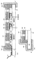
本発明のアクティブマトリクス型EL表示装置について図5と図6を用いて説明する。図5に示したのは本発明であるアクティブマトリクス型EL表示装置の画素の断面図であり、図6(A)はその上面図、図6(B)はその回路構成である。実際にはこのような画素がマトリクス状に複数配列されて画素部(画像表示部)が形成される。
【0024】
なお、図5の断面図は図6(A)に示した上面図においてA−A’で切断した切断面を示している。ここでは図5及び図6で共通の符号を用いているので、適宜両図面を参照すると良い。
【0025】
図5において、11は基板、12は下地となる絶縁膜(以下、下地膜という)である。基板11としてはガラス基板、ガラスセラミックス基板、石英基板、シリコン基板、セラミックス基板、金属基板若しくはプラスチック基板(プラスチックフィルムも含む)を用いることができる。
【0026】
また、下地膜12は特に可動イオンを含む基板や導電性を有する基板を用いる場合に有効であるが、石英基板には設けなくても構わない。下地膜12としては、珪素(シリコン)を含む絶縁膜を用いれば良い。なお、本明細書において「珪素を含む絶縁膜」とは、具体的には酸化珪素膜、窒化珪素膜若しくは窒化酸化珪素膜(SiOxNyで示される)など珪素、酸素若しくは窒素を所定の割合で含む絶縁膜を指す。
【0027】
また、下地膜12に放熱効果を持たせることによりTFTの発熱を発散させることはTFTの劣化又はEL素子の劣化を防ぐためにも有効である。その場合、アルミニウム(Al)の酸化物、窒化物などAlを成分とする合金材料で形成しても良い。
【0028】
画素内には二つのTFTを形成している。201はスイッチング用素子として機能するTFT(以下、スイッチング用TFTという)、202はEL素子へ流す電流量を制御する電流制御用素子として機能するTFT(以下、電流制御用TFTという)であり、どちらもnチャネル型TFTで形成されている。
【0029】
但し、スイッチング用TFTと電流制御用TFTをnチャネル型TFTに限定する必要はなく、両方又はどちらか片方にpチャネル型TFTを用いることも可能である。いずれにしても、電流制御用TFTに接続するEL素子にかけるバイアス電圧の極性によりTFTを選択すれば良い。
【0030】
スイッチング用TFT201は、ソース領域13、ドレイン領域14、LDD領域15a〜15d、高濃度不純物領域16及びチャネル形成領域17a、17bを含む活性層、ゲート絶縁膜18、ゲート電極19a、19b、第1層間絶縁膜20、ソース配線21並びにドレイン配線22を有して形成される。
【0031】
また、図示しないが、ゲート電極19a、19bは別の材料(ゲート電極19a、19bよりも低抵抗な材料)で形成されたゲート線によって電気的に接続されたダブルゲート構造としても良く、このような構成とすることで画面サイズの大型化に対応できる。勿論、ダブルゲート構造だけでなく、トリプルゲート構造などいわゆるマルチゲート構造(直列に接続された二つ以上のチャネル形成領域を有する活性層を含む構造)であっても良い。マルチゲート構造はオフ電流値を低減する上で極めて有効であり、本発明では画素のスイッチング素子201をマルチゲート構造とすることによりオフ電流値の低いスイッチング素子を実現している。
【0032】
また、活性層は結晶構造を含む半導体膜で形成される。即ち、単結晶半導体膜でも良いし、多結晶半導体膜や微結晶半導体膜でも良い。また、ゲート絶縁膜18は珪素を含む絶縁膜で形成すれば良い。また、ゲート電極、ソース線若しくはドレイン線はAl、タンタル(Ta)、タングステン(W)等に代表される公知の配線材料を用いることができる。
【0033】
さらに、スイッチング用TFT201においては、LDD領域15a〜15dは、ゲート絶縁膜18を介してゲート電極17a、17bと重ならないように設ける。このような構造はオフ電流値を低減する上で非常に効果的である。
【0034】
なお、チャネル形成領域とLDD領域との間にオフセット領域(チャネル形成領域と同一組成の半導体層でなり、ゲート電圧が印加されない領域)を設けることはオフ電流値を下げる上でさらに好ましい。また、二つ以上のゲート電極を有するマルチゲート構造の場合、チャネル形成領域の間に設けられた高濃度不純物領域がオフ電流値の低減に効果的である。
【0035】
以上のように、マルチゲート構造のTFTを画素のスイッチング素子201として用いることにより、十分にオフ電流値の低いスイッチング素子を実現することができる。そのため、特開平10−189252号公報の図2のようなコンデンサーを設けなくても十分な時間(選択されてから次に選択されるまでの間)電流制御用TFTのゲート電圧を維持しうる。
【0036】
即ち、従来、有効発光面積を狭める要因となっていたコンデンサーを排除することが可能となり、有効発光面積を広くすることが可能となる。このことはEL表示装置の画質を明るくできることを意味する。
【0037】
電流制御用TFT202は、ソース領域31、ドレイン領域32、LDD領域33及びチャネル形成領域34を含む活性層、ゲート絶縁膜18、ゲート電極35、第1層間絶縁膜20、ソース配線36並びにドレイン配線37を有して形成される。なお、ゲート電極35はシングルゲート構造となっているが、マルチゲート構造であっても良い。
【0038】
図6に示すように、スイッチング用TFTのドレインは電流制御用TFTのゲートに接続されている。具体的には電流制御用TFT202のゲート電極35はスイッチング用TFT201のドレイン領域14とドレイン線(接続配線とも言える)22を介して電気的に接続されている。また、ソース線36は電源供給線212に接続される。
【0039】
この電流制御用TFT202の特徴は、チャネル幅がスイッチング用TFT201のチャネル幅よりも大きい点である。即ち、図12に示すように、スイッチング用TFTのチャネル長をL1、チャネル幅をW1とし、電流制御用TFTのチャネル長をL2、チャネル幅をW2とした場合、W2/L2≧5×W1/L1(好ましくはW2/L2≧10×W1/L1)という関係式が成り立つようにする。このため、スイッチング用TFTよりも多くの電流を容易に流すことが可能である。
【0040】
なお、マルチゲート構造であるスイッチング用TFT201のチャネル長L1は、形成された二つ以上のチャネル形成領域のそれぞれのチャネル長の総和とする。図12の場合、ダブルゲート構造であるので、二つのチャネル形成領域のそれぞれのチャネル長L1a及びL1bを加えたものがスイッチング用TFT201のチャネル長L1となる。
【0041】
本発明において、チャネル長L1、L2及びチャネル幅W1、W2は特定の数値範囲に限定されるものではないが、W1は0.1〜5μm(代表的には1〜3μm)、W2は0.5〜30μm(代表的には2〜10μm)とするのが好ましい。この時、L1は0.2〜18μm(代表的には2〜15μm)、L2は0.1〜50μm(代表的には1〜20μm)とするのが好ましい。
【0042】
なお、電流制御用TFT202では電流が過剰に流れることを防止するためチャネル長Lの長さを長めに設定することが望ましい。好ましくはW2/L2≧3(好ましくはW2/L2≧5)とするとよい。望ましくはは一画素あたり0.5〜2μA(好ましくは1〜1.5μA)となるようにする。
【0043】
これらの数値範囲とすることによりVGAクラスの画素数(640×480)を有するEL表示装置からハイビジョンクラスの画素数(1920×1080又は1280×1024)を有するEL表示装置まで、あらゆる規格を網羅することができる。また、スイッチング用TFT201に形成されるLDD領域の長さ(幅)は0.5〜3.5μm、代表的には2.0〜2.5μmとすれば良い。
【0044】
また、図5に示したEL表示装置は、電流制御用TFT202において、ドレイン領域32とチャネル形成領域34との間にLDD領域33が設けられ、且つ、LDD領域33がゲート絶縁膜18を介してゲート電極35に重なっている領域と重なっていない領域とを有する点にも特徴がある。
【0045】
電流制御用TFT202は、EL素子204を発光させるための電流を供給すると同時に、その供給量を制御して階調表示を可能とする。そのため、大電流を流しても劣化しないようにホットキャリア注入による劣化対策を講じておく必要がある。また、黒色を表示する際は、電流制御用TFT202をオフ状態にしておくが、その際、オフ電流値が高いときれいな黒色表示ができなくなり、コントラストの低下等を招く。従って、オフ電流値も抑える必要がある。
【0046】
ホットキャリア注入による劣化に関しては、ゲート電極に対してLDD領域が重なった構造が非常に効果的であることが知られている。しかしながら、LDD領域全体をゲート電極に重ねてしまうとオフ電流値が増加してしまうため、本出願人はゲート電極に重ならないLDD領域を直列に設けるという新規な構造によって、ホットキャリア対策とオフ電流値対策とを同時に解決している。
【0047】
この時、ゲート電極に重なったLDD領域の長さは0.1〜3μm(好ましくは0.3〜1.5μm)にすれば良い。長すぎては寄生容量を大きくしてしまい、短すぎてはホットキャリアを防止する効果が弱くなってしまう。また、ゲート電極に重ならないLDD領域の長さは1.0〜3.5μm(好ましくは1.5〜2.0μm)にすれば良い。長すぎると十分な電流を流せなくなり、短すぎるとオフ電流値を低減する効果が弱くなる。
【0048】
また、上記構造においてゲート電極とLDD領域とが重なった領域では寄生容量が形成されてしまうため、ソース領域31とチャネル形成領域34との間には設けない方が好ましい。電流制御用TFTはキャリア(ここでは電子)の流れる方向が常に同一であるので、ドレイン領域側のみにLDD領域を設けておけば十分である。
【0049】
また、流しうる電流量を多くするという観点から見れば、電流制御用TFT202の活性層(特にチャネル形成領域)の膜厚を厚くする(好ましくは50〜100nm、さらに好ましくは60〜80nm)ことも有効である。逆に、スイッチング用TFT201の場合はオフ電流値を小さくするという観点から見れば、活性層(特にチャネル形成領域)の膜厚を薄くする(好ましくは20〜50nm、さらに好ましくは25〜40nm)ことも有効である。
【0050】
第1パッシベーション膜41の膜厚は10nm〜1μm(好ましくは200〜500nm)とすれば良い。材料としては、珪素を含む絶縁膜(特に窒化酸化珪素膜又は窒化珪素膜が好ましい)を用いることができる。このパッシベーション膜41は形成されたTFTをアルカリ金属や水分から保護する役割をもつ。最終的にTFTの上方に設けられるEL層にはナトリウム等のアルカリ金属が含まれている。即ち、第1パッシベーション膜41はこれらのアルカリ金属(可動イオン)をTFT側に侵入させない保護層としても働く。
【0051】
また、第1パッシベーション膜41に放熱効果を持たせることでEL層の熱劣化を防ぐことも有効である。但し、図5の構造のEL表示装置は基板11側に光が放射されるため、第1パッシベーション膜41は透光性を有することが必要である。また、EL層として有機材料を用いる場合、酸素との結合により劣化するので、酸素を放出しやすい絶縁膜は用いないことが望ましい。
【0052】
アルカリ金属の透過を妨げ、さらに放熱効果をもつ透光性材料としては、B(ホウ素)、C(炭素)、N(窒素)から選ばれた少なくとも一つの元素と、Al(アルミニウム)、Si(珪素)、P(リン)から選ばれた少なくとも一つの元素とを含む絶縁膜が挙げられる。例えば、窒化アルミニウム(AlxNy)に代表されるアルミニウムの窒化物、炭化珪素(SixCy)に代表される珪素の炭化物、窒化珪素(SixNy)に代表される珪素の窒化物、窒化ホウ素(BxNy)に代表されるホウ素の窒化物、リン化ホウ素(BxPy)に代表されるホウ素のリン化物を用いることが可能である。また、酸化アルミニウム(AlxOy)に代表されるアルミニウムの酸化物は透光性に優れ、熱伝導率が20Wm-1K-1であり、好ましい材料の一つと言える。これらの材料には上記効果だけでなく、水分の侵入を防ぐ効果もある。
【0053】
上記化合物に他の元素を組み合わせることもできる。例えば、酸化アルミニウムに窒素を添加して、AlNxOyで示される窒化酸化アルミニウムを用いることも可能である。この材料にも放熱効果だけでなく、水分やアルカリ金属等の侵入を防ぐ効果がある。
【0054】
また、特開昭62−90260号公報に記載された材料を用いることができる。即ち、Si、Al、N、O、Mを含む絶縁膜(但し、Mは希土類元素の少なくとも一種、好ましくはCe(セリウム),Yb(イッテルビウム),Sm(サマリウム),Er(エルビウム),Y(イットリウム)、La(ランタン)、Gd(ガドリニウム)、Dy(ジスプロシウム)、Nd(ネオジウム)から選ばれた少なくとも一つの元素)を用いることもできる。これらの材料にも放熱効果だけでなく、水分やアルカリ金属等の侵入を防ぐ効果がある。
【0055】
また、少なくともダイヤモンド薄膜又はアモルファスカーボン膜(特にダイヤモンドに特性の近いもの、ダイヤモンドライクカーボン等と呼ばれる。)を含む炭素膜を用いることもできる。これらは非常に熱伝導率が高く、放熱層として極めて有効である。但し、膜厚が厚くなると褐色を帯びて透過率が低下するため、なるべく薄い膜厚(好ましくは5〜100nm)で用いることが好ましい。
【0056】
なお、第1パッシベーション膜41の目的はあくまでアルカリ金属や水分からTFTを保護することにあるので、その効果を損なうものであってはならない。従って、上記放熱効果をもつ材料からなる薄膜を単体で用いることもできるが、これらの薄膜と、アルカリ金属や水分の透過を妨げうる絶縁膜(代表的には窒化珪素膜(SixNy)や窒化酸化珪素膜(SiOxNy))とを積層することは有効である。
【0057】
また、EL表示装置には大きく分けて四つのカラー化表示方式があり、RGBに対応した三種類のEL素子を形成する方式、白色発光のEL素子とカラーフィルターを組み合わせた方式、青色又は青緑発光のEL素子と蛍光体(蛍光性の色変換層:CCM)とを組み合わせた方式、陰極(対向電極)に透明電極を使用してRGBに対応したEL素子を重ねる方式がある。図5には一つの画素しか図示していないが、同一構造の画素が赤、緑又は青のそれぞれの色に対応して形成され、これによりカラー表示を行うことができる。これら各色のEL層は公知の材料を採用すれば良い。但し、本発明は発光方式に関わらず実施することが可能であり、上記四つの全ての方式を本発明に用いることができる。
【0058】
また、第1パッシベーション膜41を形成したら、各TFTを覆うような形で第2層間絶縁膜(平坦化膜と言っても良い)44を形成し、TFTによってできる段差の平坦化を行う。第2層間絶縁膜44としては、有機樹脂膜が好ましく、ポリイミド、ポリアミド、アクリル、BCB(ベンゾシクロブテン)等を用いると良い。勿論、十分な平坦化が可能であれば、無機膜を用いても良い。
【0059】
第2層間絶縁膜44によってTFTによる段差を平坦化することは非常に重要である。後に形成されるEL層は非常に薄いため、段差が存在することによってその部分に亀裂が入ったり、陽極と陰極が短絡したりする場合がある。従って、EL層をできるだけ平坦面に形成しうるように画素電極を形成する前に平坦化しておくことが望ましい。
【0060】
第2パッシベーション膜45はEL素子から拡散するアルカリ金属をブロッキングする重要な役割を担う。膜厚は5nm〜1μm(典型的には20〜300nm)とすれば良い。この第2パッシベーション膜45は、アルカリ金属の透過を妨げうる絶縁膜を用いる。材料としては、第1パッシベーション膜41として用いた材料を用いることができる。また、この第2パッシベーション膜45はEL素子で発生した熱を逃がしてEL素子に熱が蓄積しないように機能する放熱層としても機能する。また、第2層間絶縁膜44が有機樹脂膜である場合は熱に弱いため、EL素子で発生した熱が第2層間絶縁膜44に悪影響を与えないようにする。また、第2パッシベーション膜45は上記熱による劣化を防ぐと同時に、EL層中のアルカリ金属がTFT側へと拡散しないようにするための保護層としても機能し、さらにはEL層側へTFT側から水分や酸素が侵入しないようにする保護層としても機能する。
【0061】
前述のようにEL表示装置を作製するにあたってTFTを有機樹脂膜で平坦化することは有効であるが、EL素子で発生した熱による有機樹脂膜の劣化を考慮した構造は従来なかった。本発明では第2パッシベーション膜45を設けることによってその点を解決している点も特徴の一つと言える。
【0062】
画素電極(EL素子の陽極)46は透明導電膜であり、第2パッシベーション膜45、第2層間絶縁膜44及び第1パッシベーション膜41にコンタクトホール(開孔)を開けた後、形成された開孔部において電流制御用TFT202のドレイン配線37に接続されるように形成される。
【0063】
画素電極46が形成されたら、第2パッシベーション膜45の上に有機樹脂膜でなる分離層101を形成する。本実施例では感光性のポリイミド膜をスピンコーティング法により形成し、パターニングによって分離層101を形成する。この分離層101はインクジェット方式でEL層を形成する際の型であり、この分離層の配置によってEL素子の形成される場所が画定する。
【0064】
そして、分離層101を形成したら、次にEL層(有機材料が好ましい)47をインクジェット方式で形成する。EL層47は単層又は積層構造で用いられるが、積層構造で用いられる場合が多い。発光層、電子輸送層、電子注入層、正孔注入層又は正孔輸送層などを組み合わせて様々な積層構造が提案されているが、本発明ではいずれの構造であっても良い。また、EL層に対して蛍光性色素等をドーピングしても良い。
【0065】
本発明では既に公知のあらゆるEL材料を用いることができる。公知の材料としては、有機材料が広く知られており、駆動電圧を考慮すると有機材料を用いるのが好ましい。有機EL材料としては、例えば、以下の米国特許又は公開公報に開示された材料を用いることができる。
【0066】
米国特許第4,356,429号、米国特許第4,539,507号、米国特許第4,720,432号、米国特許第4,769,292号、米国特許第4,885,211号、米国特許第4,950,950号、米国特許第5,059,861号、米国特許第5,047,687号、米国特許第5,073,446号、米国特許第5,059,862号、米国特許第5,061,617号、米国特許第5,151,629号、米国特許第5,294,869号、米国特許第5,294,870号、特開平10−189525号公報、特開平8−241048号公報、特開平8−78159号公報。
【0067】
具体的には、正孔注入層としての有機材料は次のような一般式で表されるものを用いることができる。
【0068】
【化1】

ここでQはN又はC−R(炭素鎖)であり、Mは金属、金属酸化物又は金属ハロゲン化物であり、Rは水素、アルキル、アラルキル、アリル又はアルカリルであり、T1、T2は水素、アルキル又はハロゲンのような置換基を含む不飽和六員環である。
【0070】
また、正孔輸送層としての有機材料は芳香族第三アミンを用いることができ、好ましくは次のような一般式で表されるテトラアリルジアミンを含む。
【0071】
【化2】
ここでAreはアリレン群であり、nは1から4の整数であり、Ar、R7、R8、R9はそれぞれ選択されたアリル群である。
【0073】
また、EL層、電子輸送層又は電子注入層としての有機材料は金属オキシノイド化合物を用いることができる。金属オキシノイド化合物としては以下のような一般式で表されるものを用いれば良い。
【0074】
【化3】
ここでR2−R7は置き換え可能であり、次のような金属オキシノイド化合物を用いることもできる。
【0076】
【化4】
ここでR2−R7は上述の定義によるものであり、L1−L5は1から12の炭素元素を含む炭水化物群であり、L1、L2又はL2、L3は共にベンゾ環を形成することができる。また、次のような金属オキシノイド化合物でも良い。
【0078】
【化5】
ここでR2−R6は置き換え可能である。このように有機EL材料としては有機リガンドを有する配位化合物を含む。但し、以上の例は本発明のEL材料として用いることのできる有機EL材料の一例であって、これに限定する必要はまったくない。
【0080】
また、本発明ではEL層の形成方法としてインクジェット方式を用いるため、好ましいEL材料としてはポリマー系材料が多い。代表的なポリマー系材料としては、ポリパラフェニレンビニレン(PPV)系やポリフルオレン系などの高分子材料が挙げられる。カラー化するには、例えば、赤色発光材料にはシアノポリフェニレンビニレン、緑色発光材料にはポリフェニレンビニレン、青色発光材料にはポリフェニレンビニレン及びポリアルキルフェニレンが好ましい。
【0081】
但し、以上の例は本発明のEL材料として用いることのできる有機EL材料の一例であって、これに限定する必要はまったくない。インクジェット法に使用できる有機EL材料については、特開平10−012377号公報に記載されている材料を全て引用することができる。
【0082】
なお、インクジェット方式はバブルジェット方式(サーマルインクジェット方式ともいう)とピエゾ方式とに大別されるが、本発明を実施するにはピエゾ方式が望ましい。
【0083】
また、実際に画素電極上にEL材料を塗布するときの形状は、実施形態1で示したようにストライプ状或いは複数のドットを連続させて長円状または長方形状に形成する。分離層101はインクジェット方式でEL層を形成するに当たり隣接するEL層が相互に混合しないための機能を有している。
【0084】
カラー表示を行うには、図6で示すように赤色発光のEL層47R、緑色発光のEL層47G、青色発光のEL層47Bを形成する。このとき、それぞれのEL層を順次形成しても良いし、赤、緑、青に対応するEL層を同時に形成しても良い。また、EL形成溶液に含まれる溶媒を除去するためにベーク(焼成)処理が必要である。このベーク処理は全てのEL層を形成した後で行っても良いし、各色のEL層が形成し終えた時点で個別に行っても良い。このようにして、EL層の厚さを50〜250nmの厚さに形成する。
【0085】
図21は画素部における構成を説明するものであり、ストライプ状または長円状或いは長方形状に形成されたEL層に複数の画素電極が形成されている様子を示している。図21(A)では異なる色で発光するEL層1702a、1702bに対しそれぞれ複数の画素電極が設けられている。各画素電極にはスイッチング用TFTと電流制御用TFTの2つのTFTが接続されている。またEL層1702aと1702bは分離層1701により分離されている。マルチカラー表示するには、画素電極1703aと1703bを一組として一つの画素1710aを形成する。同様に画素1710bを隣に設けるとき、その間隔をDとするとその値はEL層の厚さの5〜10倍とする。即ち250〜2500nmとする。
【0086】
図21(B)は他の構成例を示すものであり、例えば、赤、緑、青といった様に異なる色で発光するEL層1705a、1705b、1705cに対しそれぞれ複数の画素電極が設けられている。これらのEL層は分離層1704で分離されている。マルチカラー或いはRGBフルカラー表示するには、画素電極1706a、1706b、1706cを一組として一つの画素1720aを形成する。同様に画素1710bを隣に設けるとき、その間隔をDとすると、やはりその値はEL層の厚さの5〜10倍とする。即ち250〜2500nmとする。このようにすることで画像表示を鮮明なものとすることができる。
【0087】
また、EL層47を形成する際、処理雰囲気は極力水分の少ない乾燥雰囲気とし、不活性ガス中で行うことが望ましい。EL層は水分や酸素の存在によって容易に劣化してしまうため、形成する際は極力このような要因を排除しておく必要がある。例えば、乾燥窒素雰囲気、乾燥アルゴン雰囲気等が好ましい。
【0088】
以上のようにしてEL層47をインクジェット方式により形成したら、次に陰極48、補助電極49を形成する。本明細書中では、画素電極(陽極)、EL層及び陰極で形成される発光素子をEL素子と呼ぶ。
【0089】
陰極48は仕事関数の小さいマグネシウム(Mg)、リチウム(Li)若しくはカルシウム(Ca)を含む材料を用いる。好ましくはMgAg(MgとAlをMg:Ag=10:1で混合した材料)でなる電極を用いれば良い。他にもMgAgAl電極、LiAl電極、また、LiFAl電極が挙げられる。また、補助電極49は陰極48を外部の水分等から保護膜するために設けられる電極であり、アルミニウム(Al)若しくは銀(Ag)を含む材料が用いられる。この補助電極48には放熱効果もある。
【0090】
なお、EL層47及び陰極48は大気解放せずに乾燥された不活性雰囲気中にて連続的に形成することが望ましい。これはEL層として有機材料を用いる場合、水分に非常に弱いため、大気解放した時の吸湿を避けるためである。さらに、EL層47及び陰極48だけでなく、その上の補助電極49まで連続形成するとさらに良い。
【0091】
また、第3パッシベーション膜50の膜厚は10nm〜1μm(好ましくは200〜500nm)とすれば良い。第3パッシベーション膜50を設ける目的は、EL層47を水分から保護する目的が主であるが、第2パッシベーション膜45と同様に放熱効果をもたせても良い。従って、形成材料としては第1パッシベーション膜41と同様のものを用いることができる。但し、EL層47として有機材料を用いる場合、酸素との結合により劣化する可能性があるので、酸素を放出しやすい絶縁膜は用いないことが望ましい。
【0092】
また、上述のようにEL層は熱に弱いので、なるべく低温(好ましくは室温から120℃までの温度範囲)で成膜するのが望ましい。従って、プラズマCVD法、スパッタ法、真空蒸着法、イオンプレーティング法又は溶液塗布法(スピンコーティング法)が望ましい成膜方法と言える。
【0093】
このように、第2パッシベーション膜45を設けるだけでも十分にEL素子の劣化を抑制することはできるが、さらに好ましくはEL素子を第2パッシベーション膜45及び第2パッシベーション膜50というようにEL素子を挟んで形成された二層の絶縁膜によって囲み、EL層への水分、酸素の侵入を防ぎ、EL層からのアルカリ金属の拡散を防ぎ、EL層への熱の蓄積を防ぐ。その結果、EL層の劣化がさらに抑制されて信頼性の高いEL表示装置が得られる。
【0094】
また、本発明のEL表示装置は図5のような構造の画素からなる画素部を有し、画素内において機能に応じて構造の異なるTFTが配置されている。これによりオフ電流値の十分に低いスイッチング用TFTと、ホットキャリア注入に強い電流制御用TFTとが同じ画素内に形成でき、高い信頼性を有し、且つ、良好な画像表示が可能な(動作性能の高い)EL表示装置が得られる。
【0095】
なお、図5の画素構造においてスイッチング用TFTとしてマルチゲート構造のTFTを用いているが、LDD領域の配置等の構成に関しては図1の構成に限定する必要はない。以上の構成でなる本発明について、以下に示す実施例でもってさらに詳細な説明を行うこととする。
【0096】
【実施例】
[実施例1]
本発明の実施例について図7〜図9を用いて説明する。ここでは、画素部とその周辺に設けられる駆動回路部のTFTを同時に作製する方法について説明する。但し、説明を簡単にするために、駆動回路に関しては基本回路であるCMOS回路を図示することとする。
【0097】
まず、図7(A)に示すように、ガラス基板300上に下地膜301を300nmの厚さに形成する。本実施例では下地膜302として窒化酸化珪素膜を積層して用いる。この時、ガラス基板300に接する方の窒素濃度を10〜25wt%としておくと良い。
【0098】
また、下地膜301の一部として、図5に示した第1パッシベーション膜41と同様の材料からなる絶縁膜を設けることは有効である。電流制御用TFTは大電流を流すことになるので発熱しやすく、なるべく近いところに放熱効果のある絶縁膜を設けておくことは有効である。
【0099】
次に下地膜301の上に50nmの厚さの非晶質珪素膜(図示せず))を公知の成膜法で形成する。なお、非晶質珪素膜に限定する必要はなく、非晶質構造を含む半導体膜(微結晶半導体膜を含む)であれば良い。さらに非晶質シリコンゲルマニウム膜などの非晶質構造を含む化合物半導体膜でも良い。また、膜厚は20〜100nmの厚さであれば良い。
【0100】
そして、公知の技術により非晶質珪素膜を結晶化し、結晶質珪素膜(多結晶シリコン膜若しくはポリシリコン膜ともいう)302を形成する。公知の結晶化方法としては、電熱炉を使用した熱アニール法、レーザー光を用いたレーザーアニール法、赤外光を用いたランプアニール法がある。本実施例では、XeClガスを用いたエキシマレーザー光を用いたレーザーアニール法で結晶化する。
【0101】
なお、本実施例では線状に加工したパルス発振型のエキシマレーザー光を用いるが、矩形であっても良いし、連続発振型のアルゴンレーザー光や連続発振型のエキシマレーザー光を用いることもできる。また、レーザー光の光源はエキシマレーザーに限定されるものではなく、YAGレーザーの第2高調波或いは第3高調波を用いても良い。
【0102】
本実施例では結晶質珪素膜をTFTの活性層として用いるが、非晶質珪素膜を用いることも可能である。しかし、電流制御用TFTは大電流を流す必要性があるため、電流を流しやすい結晶質珪素膜を用いた方が有利である。
【0103】
なお、オフ電流を低減する必要のあるスイッチング用TFTの活性層を非晶質珪素膜で形成し、電流制御用TFTの活性層を結晶質珪素膜で形成することは有効である。非晶質珪素膜はキャリア移動度が低いため電流を流しにくくオフ電流が流れにくい。即ち、電流を流しにくい非晶質珪素膜と電流を流しやすい結晶質珪素膜の両者の利点を生かすことができる。
【0104】
次に、図7(B)に示すように、結晶質珪素膜302上に酸化珪素膜でなる保護膜303を130nmの厚さに形成する。この厚さは100〜200nm(好ましくは130〜170nm)の範囲で選べば良い。また、珪素を含む絶縁膜であれば他の膜でも良い。この保護膜303は不純物を添加する際に結晶質珪素膜が直接プラズマに曝されないようにするためと、微妙な濃度制御を可能にするために設ける。
【0105】
そして、その上にレジストマスク304a、304bを形成し、保護膜303を介してn型を付与する不純物元素(以下、n型不純物元素という)を添加する。なお、n型不純物元素としては、代表的には15族に属する元素、典型的にはリン又は砒素を用いることができる。なお、本実施例ではフォスフィン(PH3)を質量分離しないでプラズマ励起したプラズマドーピング法を用い、リンを1×10¹⁸atoms/cm3の濃度で添加する。勿論、質量分離を行うイオンインプランテーション法を用いても良い。
【0106】
この工程により形成されるn型不純物領域305、306には、n型不純物元素が2×10¹⁶〜5×10¹⁹atoms/cm3(代表的には5×1017〜5×1018atoms/cm3)の濃度で含まれるようにドーズ量を調節する。
【0107】
次に、図7(C)に示すように、保護膜303を除去し、添加した15族に属する元素の活性化を行う。活性化手段は公知の技術を用いれば良いが、本実施例ではエキシマレーザー光の照射により活性化する。勿論、パルス発振型でも連続発振型でも良いし、エキシマレーザー光に限定する必要はない。但し、添加された不純物元素の活性化が目的であるので、結晶質珪素膜が溶融しない程度のエネルギーで照射することが好ましい。なお、保護膜303をつけたままレーザー光を照射しても良い。尚、このレーザー光による不純物元素の活性化に際して、熱処理による活性化を併用しても構わない。熱処理による活性化を行う場合は、基板の耐熱性を考慮して450〜550℃程度の熱処理を行えば良い。
【0108】
この工程によりn型不純物領域305、306の端部、即ち、n型不純物領域305、306の周囲に存在するn型不純物元素を添加していない領域との境界部(接合部)が明確になる。このことは、後にTFTが完成した時点において、LDD領域とチャネル形成領域とが非常に良好な接合部を形成しうることを意味する。
【0109】
次に、図7(D)に示すように、結晶質珪素膜の不要な部分を除去して、島状の半導体膜(以下、活性層という)307〜310を形成する。
【0110】
次に、図7(E)に示すように、活性層307〜310を覆ってゲート絶縁膜311を形成する。ゲート絶縁膜311としては、10〜200nm、好ましくは50〜150nmの厚さの珪素を含む絶縁膜を用いれば良い。これは単層構造でも積層構造でも良い。本実施例では110nm厚の窒化酸化珪素膜を用いる。
【0111】
次に、200〜400nm厚の導電膜を形成し、パターニングしてゲート電極312〜316を形成する。なお、本実施例ではゲート電極と、ゲート電極に電気的に接続された引き回しのための配線(以下、ゲート配線という)とを別の材料で形成する。具体的にはゲート電極よりも低抵抗な材料をゲート配線として用いる。これは、ゲート電極としては微細加工が可能な材料を用い、ゲート配線には微細加工はできなくとも配線抵抗が小さい材料を用いるためである。勿論、ゲート電極とゲート配線とを同一材料で形成してしまっても構わない。
【0112】
また、ゲート電極は単層の導電膜で形成しても良いが、必要に応じて二層、三層といった積層膜とすることが好ましい。ゲート電極の材料としては公知のあらゆる導電膜を用いることができる。ただし、上述のように微細加工が可能、具体的には2μm以下の線幅にパターニング可能な材料が好ましい。
【0113】
代表的には、タンタル(Ta)、チタン(Ti)、モリブデン(Mo)、タングステン(W)、クロム(Cr)、導電性を有するシリコン(Si)から選ばれた元素でなる膜、または前記元素の窒化物膜(代表的には窒化タンタル膜、窒化タングステン膜、窒化チタン膜)、または前記元素を組み合わせた合金膜(代表的にはMo−W合金、Mo−Ta合金)、または前記元素のシリサイド膜(代表的にはタングステンシリサイド膜、チタンシリサイド膜)を用いることができる。勿論、単層で用いても積層して用いても良い。本実施例では、50nm厚の窒化タンタル(TaN)膜と、350nm厚のTa膜とでなる積層膜を用いる。これはスパッタ法で形成すれば良い。また、スパッタガスとしてXe、Ne等の不活性ガスを添加すると応力による膜はがれを防止することができる。
【0114】
この時、ゲート電極313、316はそれぞれn型不純物領域305、306の一部とゲート絶縁膜311を介して重なるように形成する。この重なった部分が後にゲート電極と重なったLDD領域となる。
【0115】
次に、図8(A)に示すように、ゲート電極312〜316をマスクとして自己整合的にn型不純物元素(本実施例ではリン)を添加する。こうして形成される不純物領域317〜323にはn型不純物領域305、306の1/2〜1/10(代表的には1/3〜1/4)の濃度でリンが添加されるように調節する。具体的には、1×1016〜5×1018atoms/cm3(典型的には3×1017〜3×1018atoms/cm3)の濃度が好ましい。
【0116】
次に、図8(B)に示すように、ゲート電極等を覆う形でレジストマスク324a〜324cを形成し、n型不純物元素(本実施例ではリン)を添加して高濃度にリンを含む不純物領域325〜331を形成する。ここでもフォスフィン(PH3)を用いたイオンドープ法で行い、この領域のリンの濃度は1×10²⁰〜1×10²¹atoms/cm3(代表的には2×1020〜5×1021atoms/cm3)となるように調節する。
【0117】
この工程によってnチャネル型TFTのソース領域若しくはドレイン領域が形成されるが、スイッチング用TFTでは、図8(A)の工程で形成したn型不純物領域320〜322の一部を残す。この残された領域が、図5におけるスイッチング用TFTのLDD領域15a〜15dに対応する。
【0118】
次に、図8(C)に示すように、レジストマスク324a〜324cを除去し、新たにレジストマスク332を形成する。そして、p型不純物元素(本実施例ではボロン)を添加し、高濃度にボロンを含む不純物領域333、334を形成する。ここではジボラン(B2H6)を用いたイオンドープ法により3×10²⁰〜3×10²¹atoms/cm3(代表的には5×1020〜1×1021atoms/cm3ノ)濃度となるようにボロンを添加する。
【0119】
なお、不純物領域333、334には既に1×10²⁰〜1×10²¹atoms/cm3の濃度でリンが添加されているが、ここで添加されるボロンはその少なくとも3倍以上の濃度で添加される。そのため、予め形成されていたn型の不純物領域は完全にP型に反転し、P型の不純物領域として機能する。
【0120】
次に、レジストマスク332を除去した後、それぞれの濃度で添加されたn型またはp型不純物元素を活性化する。活性化手段としては、ファーネスアニール法、レーザーアニール法、またはランプアニール法で行うことができる。本実施例では電熱炉において窒素雰囲気中、550℃、4時間の熱処理を行う。
【0121】
このとき雰囲気中の酸素を極力排除することが重要である。なぜならば酸素が少しでも存在していると露呈したゲート電極の表面が酸化され、抵抗の増加を招くと共に後にオーミックコンタクトを取りにくくなるからである。従って、上記活性化工程における処理雰囲気中の酸素濃度は1ppm以下、好ましくは0.1ppm以下とすることが望ましい。
【0122】
次に、活性化工程が終了したら図8(D)に示すように300nm厚のゲート線335を形成する。ゲート配線335の材料としては、アルミニウム(Al)又は銅(Cu)を主成分(組成として50〜100%を占める。)とする金属膜を用いれば良い。配置としては図2のゲート配線211のように、スイッチング用TFTのゲート電極314、315(図2のゲート電極19a、19bに相当する)を電気的に接続するように形成する。
【0123】
このような構造とすることでゲート配線の配線抵抗を非常に小さくすることができるため、面積の大きい画像表示領域(画素部)を形成することができる。即ち、画面の大きさが対角10インチ以上(さらには30インチ以上)のEL表示装置を実現する上で、本実施例の画素構造は極めて有効である。
【0124】
次に、図9(A)に示すように、第1層間絶縁膜336を形成する。第1層間絶縁膜336としては、珪素を含む絶縁膜を単層で用いるか、その中で組み合わせた積層膜を用いれば良い。また、膜厚は400nm〜1.5μmとすれば良い。本実施例では、200nm厚の窒化酸化珪素膜の上に800nm厚の酸化珪素膜を積層した構造とする。
【0125】
さらに、3〜100%の水素を含む雰囲気中で、300〜450℃で1〜12時間の熱処理を行い水素化処理を行う。この工程は熱的に励起された水素により半導体膜の不対結合手を水素終端する工程である。水素化の他の手段として、プラズマ水素化(プラズマにより励起された水素を用いる)を行っても良い。尚、水素化処理は第1層間絶縁膜336を形成する間に入れても良い。即ち、200nm厚の窒化酸化珪素膜を形成した後で上記のように水素化処理を行い、その後で残り800nm厚の酸化珪素膜を形成しても構わない。
【0126】
次に、第1層間絶縁膜336に対してコンタクトホールを形成し、ソース配線337〜340と、ドレイン配線341〜343を形成する。なお、本実施例ではこの電極を、Ti膜を100nm、Tiを含むアルミニウム膜を300nm、Ti膜150nmをスパッタ法で連続形成した3層構造の積層膜とする。勿論、他の導電膜でも良い。
【0127】
次に、50〜500nm(代表的には200〜300nm)の厚さで第1パッシベーション膜344を形成する。本実施例では第1パッシベーション膜344として300nm厚の窒化酸化珪素膜を用いる。これは窒化珪素膜で代用しても良い。勿論、図5の第1パッシベーション膜41と同様の材料を用いることが可能である。
【0128】
なお、窒化酸化珪素膜の形成に先立ってH2、NH3等水素を含むガスを用いてプラズマ処理を行うことは有効である。この前処理により励起された水素が第1層間絶縁膜336に供給され、熱処理を行うことで、第1パッシベーション膜344の膜質が改善される。それと同時に、第1層間絶縁膜336に添加された水素が下層側に拡散するため、効果的に活性層を水素化することができる。
【0129】
次に、有機樹脂からなる第2層間絶縁膜347を形成する。有機樹脂としてはポリイミド、ポリアミド、アクリル、BCB(ベンゾシクロブテン)等を使用することができる。特に、第2層間絶縁膜346は平坦化の意味合いが強いので、平坦性に優れたアクリルが好ましい。本実施例ではTFTによって形成される段差を十分に平坦化しうる膜厚でアクリル膜を形成する。好ましくは1〜5μm(さらに好ましくは2〜4μm)とすれば良い。
【0130】
次に、第2層間絶縁膜347上に100nm厚の第2パッシベーション膜348を形成する。本実施例ではSi、Al、N、O及びLaを含む絶縁膜を用いるため、その上に設けられるEL層からのアルカリ金属の拡散を防止することができる。また、同時にEL層に水分を侵入させず、且つ、EL層で発生した熱を分散させて、熱によるEL層の劣化や平坦化膜(第2層間絶縁膜)の劣化を抑制することができる。
【0131】
そして、第2パッシベーション膜348、第2層間絶縁膜347及び第1パッシベーション膜344にドレイン配線343に達するコンタクトホールを形成し、画素電極349を形成する。本実施例では酸化インジウム・スズ(ITO)膜を110nmの厚さに形成し、パターニングを行って画素電極とする。この画素電極349がEL素子の陽極となる。なお、他の材料として、酸化インジウム・チタン膜や酸化インジウム・亜鉛膜を用いることも可能である。
【0132】
尚、本実施例では画素電極349がドレイン配線343を介して電流制御用TFTのドレイン領域331へと電気的に接続された構造となっている。この構造には次のような利点がある。
【0133】
画素電極349はEL層(発光層)や電荷輸送層などの有機材料に直接接することになるため、EL層等に含まれた可動イオンが画素電極中を拡散する可能性がある。即ち、本実施例の構造は画素電極349を直接活性層の一部であるドレイン領域331へ接続せず、ドレイン配線343を中継することによって活性層中への可動イオンの侵入を防ぐことができる。
【0134】
次に、図9(C)に示すように、EL層350をインクジェット方式により形成し、さらに大気解放しないで陰極(MgAg電極)351、補助電極352を形成する。このときEL層350及び陰極351を形成するに先立って画素電極349に対して熱処理を施し、水分を完全に除去しておくことが望ましい。なお、本実施例ではEL素子の陰極としてMgAg電極を用いるが、公知の他の材料であっても良い。
【0135】
尚、EL層350としては実施形態2で説明した材料を用いることができる。例えば、正孔注入層(Hole injecting layer)、正孔輸送層(Hole transporting layer)、発光層(Emitting layer)及び電子輸送層(Electron transporting layer)でなる4層構造をEL層としても良いし、電子輸送層を設けない場合もあり、電子注入層を設ける場合もある。また、正孔注入層を省略する場合もある。このように組み合わせは既に様々な例が報告されており、そのいずれの構成を用いても構わない。
【0136】
正孔注入層又は正孔輸送層としてはアミン系のTPD(トリフェニルアミン誘導体)を用いればよく、他にもヒドラゾン系(代表的にはDEH)、スチルベン系(代表的にはSTB)、スターバスト系(代表的にはm−MTDATA)等を用いることができる。特にガラス転移温度が高く結晶化しにくいスターバスト系材料が好ましい。
【0137】
発光層としては赤色発光層としてはBPPC、ペリレン、DCMが用いることができるが、特にEu(DBM)3(Phen)で示されるEu錯体(J.Kido et.al,Appl.Phys.,vol.35,pp.L394-396,1996に詳しい。)は620nmの波長に鋭い発光をもち単色性が高い。
【0138】
また、緑色発光層として代表的にはAlq3(8-hydroxyquinoline alminium)に数モル%のキナクリドン又はクマリンを添加した材料を用いることができる。化学式は以下のようになる。
【0139】
【化6】
また、青色発光層として代表的にはDSA(ジスチルアリーレン誘導体)にアミノ置換DSAを添加したジスチルアリーレンアミン誘導体を用いることができる。特に、性能の高い材料であるジスチリルビフェニル(DPVBi)を用いることが好ましい。化学式は以下のようになる。
【0141】
【化7】
また、補助電極352でもEL層350を水分や酸素から保護することは可能であるが、さらに好ましくは第3パッシベーション膜353を設けると良い。本実施例では第3パッシベーション膜353として300nm厚の窒化珪素膜を設ける。この第3パッシベーション膜も補助電極352の後に大気解放しないで連続的に形成しても構わない。勿論、第3パッシベーション膜353としては、図5の第3パッシベーション膜50と同一の材料を用いることができる。
【0143】
補助電極352はMgAg電極351の劣化を防ぐために設けられ、Alを主成分とする金属膜が代表的である。勿論、他の材料でも良い。また、EL層350、MgAg電極351は非常に水分に弱いので、補助電極352までを大気解放しないで連続的に形成し、外気からEL層を保護することが望ましい。
【0144】
尚、EL層350の膜厚は10〜400nm(典型的には60〜160nm)、MgAg電極351の厚さは180〜300nm(典型的には200〜250nm)とすれば良い。また、EL層350を積層構造とする場合、各層の膜厚は10〜100nmの範囲とすれば良い。
【0145】
こうして図9(C)に示すような構造のアクティブマトリクス型EL表示装置が完成する。ところで、本実施例のアクティブマトリクス型EL表示装置は、画素部だけでなく駆動回路部にも最適な構造のTFTを配置することにより、非常に高い信頼性を示し、動作特性も向上しうる。
【0146】
まず、極力動作速度を落とさないようにホットキャリア注入を低減させる構造を有するTFTを、駆動回路を形成するCMOS回路のnチャネル型TFT205として用いる。なお、ここでいう駆動回路としては、シフトレジスタ、バッファ、レベルシフタ、サンプリング回路(サンプル及びホールド回路)などが含まれる。デジタル駆動を行う場合には、D/Aコンバータなどの信号変換回路も含まれうる。
【0147】
本実施例の場合、図9(C)に示すように、nチャネル型205の活性層は、ソース領域355、ドレイン領域356、LDD領域357及びチャネル形成領域358を含み、LDD領域357はゲート絶縁膜311を介してゲート電極313と重なっている。
【0148】
ドレイン領域側のみにLDD領域を形成しているのは、動作速度を落とさないための配慮である。また、このnチャネル型TFT205はオフ電流値をあまり気にする必要はなく、それよりも動作速度を重視した方が良い。従って、LDD領域357は完全にゲート電極に重ねてしまい、極力抵抗成分を少なくすることが望ましい。即ち、いわゆるオフセットはなくした方がよい。
【0149】
また、CMOS回路のpチャネル型TFT206は、ホットキャリア注入による劣化が殆ど気にならないので、特にLDD領域を設けなくても良い。勿論、nチャネル型TFT205と同様にLDD領域を設け、ホットキャリア対策を講じることも可能である。尚、駆動回路の中でもサンプリング回路は他の回路と比べて少し特殊であり、チャネル形成領域を双方向に大電流が流れる。即ち、ソース領域とドレイン領域の役割が入れ替わるのである。さらに、オフ電流値を極力低く抑える必要があり、そういった意味でスイッチング用TFTと電流制御用TFTの中間程度の機能を有するTFTを配置することが望ましい。
【0150】
従って、サンプリング回路を形成するnチャネル型TFTは、図13に示すような構造のTFTを配置することが望ましい。図13に示すように、LDD領域901a、901bの一部がゲート絶縁膜902を介してゲート電極903と重なる。この効果は電流制御用TFT202の説明で述べた通りであり、サンプリング回路の場合はチャネル形成領域904を挟む形で設ける点が異なる。
【0151】
また、図5に示したような構造の画素を形成して画素部を形成している。画素内に形成されるスイッチング用TFT及び電流制御用TFTの構造については、図5で既に説明したのでここでの説明は省略する。
【0152】
なお、実際には図9(C)まで完成したら、さらに外気に曝されないように気密性の高い保護フィルム(ラミネートフィルム、紫外線硬化樹脂フィルム等)やセラミックス製シーリングカンなどのハウジング材でパッケージング(封入)することが好ましい。その際、ハウジング材の内部を不活性雰囲気にしたり、内部に吸湿性材料(例えば酸化バリウム)を配置することでEL層の信頼性(寿命)が向上する。
【0153】
また、パッケージング等の処理により気密性を高めたら、基板上に形成された素子又は回路から引き回された端子と外部信号端子とを接続するためのコネクター(フレキシブルプリントサーキット:FPC)を取り付けて製品として完成する。このような出荷できる状態にまでしたEL表示装置を本明細書中ではELモジュールという。
【0154】
ここで本実施例のアクティブマトリクス型EL表示装置の構成を図10の斜視図を用いて説明する。本実施例のアクティブマトリクス型EL表示装置は、ガラス基板601上に形成された、画素部602と、ゲート側駆動回路603と、ソース側駆動回路604で構成される。画素部のスイッチング用TFT605はnチャネル型TFTであり、ゲート側駆動回路603に接続されたゲート配線606、ソース側駆動回路604に接続されたソース配線607の交点に配置されている。また、スイッチング用TFT605のドレインは電流制御用TFT608のゲートに接続されている。
【0155】
さらに、電流制御用TFT606のソース側は電源供給線609に接続される。本実施例のような構造では、電源供給線609には接地電位(アース電位)が与えられている。また、電流制御用TFT608のドレインにはEL素子610が接続されている。また、このEL素子610のカソードには所定の電圧(本実施例では10〜12V)が加えられる。そして、外部入出力端子となるFPC611には駆動回路まで信号を伝達するための入出力配線(接続配線)612、613、及び電源供給線609に接続された入出力配線614が設けられている。
【0156】
また、図10に示したEL表示装置の回路構成の一例を図11に示す。図11の回路構成はアナログ駆動の例であり、ソース側駆動回路701、ゲート側駆動回路(A)707、ゲート側駆動回路(B)711、画素部706を有している。なお、本明細書中において、駆動回路とはソース側処理回路およびゲート側駆動回路を含めた総称である。
【0157】
ソース側駆動回路701は、シフトレジスタ702、レベルシフタ703、バッファ704、サンプリング回路(サンプル及びホールド回路)705を備えている。また、ゲート側駆動回路(A)707は、シフトレジスタ708、レベルシフタ709、バッファ710を備えている。ゲート側駆動回路(B)711も同様な構成である。
【0158】
ここで、シフトレジスタ702、708は駆動電圧が5〜16V(代表的には10V)であり、回路を形成するCMOS回路に使われるnチャネル型TFTは図9(C)の205で示される構造が適している。
【0159】
また、レベルシフタ703、709、バッファ704、710は、駆動電圧は14〜16Vと高くなるが、シフトレジスタと同様に、図9(C)のnチャネル型TFT205を含むCMOS回路が適している。なお、ゲート配線をダブルゲート構造、トリプルゲート構造といったマルチゲート構造とすることは、各回路の信頼性を向上させる上で有効である。また、サンプリング回路705は駆動電圧が14〜16Vであるが、ソース領域とドレイン領域が反転する上、オフ電流値を低減する必要があるので、図13のnチャネル型TFT208を含むCMOS回路が適している。画素部706は駆動電圧が14〜16Vであり、図5に示した構造の画素を配置する。
【0160】
上記構成は、図7〜9に示した作製工程に従ってTFTを作製することによって容易に実現することができる。また、本実施例では画素部と駆動回路の構成のみ示しているが、本実施例の作製工程に従えば、その他にも信号分割回路、D/Aコンバータ回路、オペアンプ回路、γ補正回路など駆動回路以外の論理回路を同一基板上に形成することが可能であり、さらにはメモリ部やマイクロプロセッサ等を形成しうると考えている。
【0161】
さらに、ハウジング材をも含めた本実施例のELモジュールについて図14、図15を用いて説明する。なお、必要に応じて図10、図11で用いた符号を引用することにする。
【0162】
図14において、601は基板、602は画素部、603はソース側駆動回路、604はゲート側駆動回路、612は画素部602、ソース側駆動回路603、ゲート側駆動回路604をFPC(フレキシブルプリントサーキット)611に電気的に接続するための接続配線である。また、FPCは外部機器へと電気的に接続され、これにより画素部602、ソース側駆動回路603及びゲート側駆動回路604に外部からの信号を入力することができる。画素部602、ソース側駆動回路603及びゲート側駆動回路604は基板601上に形成された薄膜トランジスタ(以下、TFTという)で形成されている。なお、TFTとしては如何なる構造のTFTを用いても良い。勿論、公知の構造であっても良い。さらに、充填材(図示せず)、カバー材1407、シール材(図示せず)及びフレーム材1408が形成される。
【0163】
ここで、図14をA−A’で切断した断面図を図15(A)に、B−B’で切断した断面図を図15(B)に示す。なお、図15(A)、(B)では図14と同一の部位に同一の符号を用いている。
【0164】
図15(A)に示すように、基板601上に画素部602、駆動回路603が形成されており、画素部602は電流制御用TFT1501とそれに電気的に接続された画素電極1502を含む複数の画素により形成される。この画素電極1502はEL素子の陽極として機能する。また、画素電極1502を覆うようにEL層1503が形成され、その上にはEL素子の陰極1504が形成される。
【0165】
陰極1504は全画素に共通の配線としても機能し、接続配線612を経由してFPC611に電気的に接続されている。さらに、画素部602及び駆動回路603に含まれる素子は全てパッシベーション膜1507で覆われている。
【0166】
さらに、EL素子を覆うようにして充填材1508を設ける。この充填材1508はカバー材1407を接着するための接着剤としても機能する。充填材1508としては、PVC(ポリビニルクロライド)、エポキシ樹脂、シリコーン樹脂、PVB(ポリビニルブチラル)またはEVA(エチレンビニルアセテート)を用いることができる。この充填材1508の内部に乾燥剤を設けておくと、吸湿効果を保ち続けられるので好ましい。
【0167】
また、カバー材1407としては、ガラス板、アルミニウム板、ステンレス板、FRP(Fiberglass-Reinforced Plastics)板、PVF(ポリビニルフロライド)フィルム、マイラーフィルム、ポリエステルフィルムまたはアクリルフィルムを用いることができる。なお、充填材1508としてPVBやEVAを用いる場合、数十μmのアルミニウムホイルをPVFフィルムやマイラーフィルムで挟んだ構造のシートを用いることが好ましい。
【0168】
但し、EL素子からの発光方向(光の放射方向)によってはカバー材1407が透光性を有する必要がある。即ち、図15の場合はカバー材1407の反対側に光が放射されるので材質は問わないが、カバー材1407側に放射されるような場合はカバー材1407に透光性の高い部材を用いる。
【0169】
次に、充填材1508を用いてカバー材1407を接着した後、充填材1508の側面(露呈面)を覆うようにフレーム材1408を取り付ける。フレーム材1408はシール材(接着剤として機能する)1509によって接着される。このとき、シール材1509としては、光硬化性樹脂を用いるのが好ましいが、EL層の耐熱性が許せば熱硬化性樹脂を用いても良い。なお、シール材1509はできるだけ水分や酸素を透過しない材料であることが望ましい。また、シール材1509の内部に乾燥剤を添加してあっても良い。
【0170】
以上のような方式を用いてEL素子を充填材1508に封入することにより、EL素子を外部から完全に遮断することができ、外部から水分や酸素等のEL層の酸化による劣化を促す物質が侵入することを防ぐことができる。従って、信頼性の高いEL表示装置を作製することができる。
【0171】
[実施例2]
実施例1ではTFTを形成した基板側にEL素子で発光した光を放射する形式のEL表示装置について示した。この場合には、少なくともTFTが形成された領域は影となり、その分画素部の開口率は低下する。一方、EL素子で発光した光を上方(TFTが形成された基板の反対側)に放射する形式とすると、少なくとも開口率を向上させることは容易となる。
【0172】
図18は上方に光を放射する形式のEL表示素子の構成を示す。スイッチング用TFT201と電流制御用TFT202の構成は実施形態2と同様なものであり、ここではその他の部分の差異について説明する。
【0173】
電流制御用TFT202のドレイン側に接続する陰極側画素電極949は第2パッシベーション膜945上に形成する。分離層951は有機樹脂材料で形成する。そして、陰極948をMgAg(MgとAlをMg:Ag=10:1で混合した材料)、MgAgAl、LiAl、LiFAl等の材料を用いて形成する。
【0174】
EL層947も実施形態1または実施形態2と同様にしてインクジェット方式で形成する。さらに、ITOなどの透明導電膜材料で陽極側画素電極を形成し、その上に第3パッシベーション膜950を形成して上方に光を放射する形式のEL表示素子が完成する。
【0175】
[実施例3]
本発明のインクジェット方式によるEL層の作製方法、及び作製されたEL層はパッシブ型のEL表示装置にも適用できる。その実施例を図16を用いて説明する。
【0176】
図16(A)において基板1601はコーニング社の#1737ガラス基板に代表される無アルカリガラス基板、結晶化ガラス基板、表面に酸化珪素または窒化珪素等を形成したソーダライムガラス基板、プラスチック基板などを適用することができる。基板1601上には透明電極1602が50〜200nmの厚さに形成され、エッチング処理やリフトオフ法等の手法により短冊状に複数個に分割する。透明電極1601はITO、ZnO、SnO2、ITO−ZnO等の材料で形成する。そして、ポリイミド等の有機樹脂材料を用いて、短冊状に形成した透明電極1602の側端部に接するように分離層1603を0.5〜2μmの厚さで形成する。
【0177】
EL層は単層又は積層構造で用いられる。積層構造は、発光層、電子輸送層、電子注入層、正孔注入層又は正孔輸送層などを組み合わせた積層構造で形成されるが、本実施例では正孔注入層と発光層を積層させた構造で形成する。まず、図16(B)に示すように正孔注入層1606を形成する。正孔注入層は必ずしも必要なものではないが、発光効率の向上のために設けると好ましい場合がある。正孔注入層の材料は実施形態1で示したように、テトラアリルジアミンを含む有機材料で形成する。この場合もインクジェット方式を用い、インクヘッド1604から吐出した溶液1605を、分離層の間にストライプ状、または複数のドットを連結させて長円状または長方形状に形成する。その後、ホットプレート等により100℃程度に加熱し不要な水分等を蒸発させる。
【0178】
図16(C)に示すように発光層もインクジェット方式で形成する。カラー表示をする場合には、赤、緑、青の各色のシリンダーを有するインクヘッドを用い、発光材料を含有するEL形成溶液1609を正孔注入層上に吐出させて形成する。発光層1608は、好ましいEL材料として、ポリパラフェニレンビニレン(PPV)系やポリフルオレン系などの高分子材料がある。カラー化するには、例えば、赤色発光材料にはシアノポリフェニレンビニレン、緑色発光材料にはポリフェニレンビニレン、青色発光材料にはポリフェニレンビニレン及びポリアルキルフェニレンが好ましい。このようにして、赤、緑、青の各色に対応した発光層1608R、1608G、1608Bをストライプ状、または複数のを連結させて長円状または長方形状に形成する。インクジェット方式においても、形成時にEL材料が酸化して劣化するのを防ぐために窒素またはアルゴン等の不活性ガス雰囲気中で作業を行うようにする。
【0179】
そして、陰極材料をMgAg(MgとAgをMg:Ag=10:1で混合した材料)、MgAgAl、LiAl、LiFAl等の材料で形成する。この陰極材料は、代表的には真空蒸着法で1〜50nmの厚さで形成する。さらにこの上に補助電極としてAlなどを積層させる。図16(D)の陰極層1610はこのような構成を示し、それぞれの膜形成時にマスク部材を用い短冊状に形成する。短冊状に形成された陰極層1610は、やはり同様に短冊状に形成した透明電極1602とほぼ直交するように形成する。この陰極層1610上には窒化珪素膜、窒化酸化珪素膜などでパッシベーション膜1611が形成される。
【0180】
ここで示したEL層を形成する材料は水分や湿気等に弱いためハウジング材で封止することが望ましい。ハウジング材1614の材質はガラス、ポリマー等の絶縁性物質が好ましい。例えば、非晶質ガラス(硼硅酸塩ガラス、石英等)、結晶化ガラス、セラミックスガラス、有機系樹脂(アクリル系樹脂、スチレン系樹脂、ポリカーボネート系樹脂、エポキシ系樹脂等)、シリコーン系樹脂が挙げられる。また、セラミックスを用いても良い。また、接着剤1705が絶縁性物質であるならステンレス合金等の金属材料を用いることも可能である。
【0181】
また、ハウジング材1614をEL層が形成された基板に張り合わせる接着剤1612の材質は、エポキシ系樹脂、アクリレート系樹脂等の接着剤を用いることが可能である。さらに、熱硬化性樹脂や光硬化性樹脂を接着剤として用いることもできる。但し、可能な限り酸素、水分を透過しない材質であることが必要である。接着剤1612には酸化バリウム等の乾燥剤1613を混入させておいても良い。このようにしてパッシブ型のEL表示装置を形成することができる。
【0182】
[実施例4]
EL素子を形成する薄膜形成装置の一例を図17に示す。図17に示したのは発光層として高分子系有機EL層、陰極層として周期律表の1族若しくは2族に属する元素を含む金属膜、補助電極としてAl等の導電膜、パッシベーション膜を連続して形成する装置である。
【0183】
図17において、401は基板の搬入または搬出を行う搬送室であり、ロード・アンロード室とも呼ばれる。ここに基板をセットしたキャリア402が配置される。尚、搬送室401は基板搬入用と基板搬出用と区別されていても良い。また、403は基板404を搬送する機構(以下、搬送機構という)405を含む共通室である。基板のハンドリングを行うロボットアームなどは搬送機構(1)405の一種である。
【0184】
共通室403にはゲート406a〜406fを介して複数の処理室が連結されている。図17の構成では共通室403を数mTorrから数十mTorrに減圧し、各処理室はゲート406a〜406fによって共通室403とは遮断されている。この場合、インクジェット印刷用処理室415とスピンコート用処理室408は窒素またはアルゴン等の不活性ガスを満たした常圧中で行われるため、共通室403との間に、真空排気用処理室412を設けた構成となっている。
【0185】
減圧下で所定の作業を行う各処理室には排気ポンプを設けることで真空下での処理を行うことが可能となる。排気ポンプとしては、油回転ポンプ、メカニカルブースターポンプ、ターボ分子ポンプ若しくはクライオポンプを用いることが可能であるが、水分の除去に効果的なクライオポンプが好ましい。
【0186】
発光層や注入層から成るEL層の形成は、インクジェット印刷用処理室415、またはスピンコート用処理室408で行う。インクジェット印刷用処理室415には基板保持手段や図3で説明したインクヘッド等が設けられている。また、前述のように有機EL材料は水分に極めて弱いため、インクジェット印刷用処理室415、スピンコート用処理室408は常に不活性雰囲気に保たれている。
【0187】
基板の搬送は、まず真空排気用処理室412を共通室403と同じ圧力まで減圧しておき、その状態でゲート406dを開けて基板を搬送する。そして、ゲート406dを閉めた後、真空排気用処理室412内を不活性ガスでパージし、常圧に戻った時点でゲート413を開けて基板搬送室414にある搬送機構(2)418で基板をインクジェット印刷用処理室415、スピンコート用処理室408に搬送する。
【0188】
本発明では有機EL層はインクジェット方式で形成するものであるが、発光層をインクジェット方式で形成し、正孔または電子注入層や正孔または電子輸送層などの一部の層をスピンコート法で形成するといったように両者を適宣組み合わせて形成しても良い。
【0189】
EL層の形成工程が終了したら、ゲート413を開けて真空排気用処理室412へ基板を搬送し、ゲート413及びゲート406dを閉めた状態で真空排気を行う。真空排気用処理室412が共通室403と同じ減圧状態にまで達したら、ゲート406dを開けて基板を共通室へと搬送する。
【0190】
尚、ここでは焼成用処理室409を設けているが、真空排気用処理室412のサセプターを加熱できるようにして、ここで焼成工程を行っても良い。焼成後に真空排気することで、脱ガスを抑えることが可能である。
【0191】
第1成膜用処理室410では陰極の形成を行う。陰極材料としては、公知の材料を用いて行う。陰極は真空蒸着法で形成するが、そのとき基板表面(高分子系EL層が形成された面)は、上向き(フェイスアップ方式)であっても下向き(フェイスダウン方式)であっても良い。
【0192】
フェイスアップ方式の場合、共通室403から搬送された基板をそのままサセプターに設置すれば良いため非常に簡易である。フェイスダウン方式の場合、搬送機構(1)405若しくは第1成膜用処理室410に、基板を反転させるための機構を備えておく必要が生じるため搬送機構が複雑になるが、ゴミの付着が少ないという利点が得られる。
【0193】
尚、第1成膜用処理室110において蒸着処理を行う場合には、蒸着源を具備しておく必要がある。蒸着源は複数設けても良い。また、抵抗加熱方式の蒸着源としても良いし、EB(電子ビーム)方式の蒸着源としても良い。
【0194】
第2成膜用処理室411は、気相成膜法により電極を形成するための処理室である。ここでは陰極を補助するための補助電極の形成が行われる。また、蒸着法又はスパッタ法が用いられるが、蒸着法の方がダメージを与えにくいので好ましい。いずれにしてもゲート406fによって共通室403と遮断され、真空下で成膜が行われる。尚、気相成膜法として蒸着法を行う場合には、蒸着源を設ける必要がある。蒸着源に関しては第1気相成膜用処理室410と同様で構わないので、ここでの説明は省略する。
【0195】
陰極として良く用いられる金属膜は、周期律表の1族若しくは2族に属する元素を含む金属膜であるが、これらの金属膜は酸化しやすいので表面を保護しておくことが望ましい。また、必要な膜厚も薄いため、抵抗率の低い導電膜を補助的に設けて陰極の抵抗を下げ、加えて陰極の保護を図る。抵抗率の低い導電膜としてはアルミニウム、銅又は銀を主成分とする金属膜が用いられる。
【0196】
次に、第3成膜用処理室407では、第3パッシベーション膜を形成するための処理室である。第3パッシベーション膜は窒化珪素膜または窒化酸化珪素膜等をプラズマCVD法で形成する。従って、図示していないが、SiH4、N2O、NH3などのガス供給系、13.56〜60MHzの高周波電源を用いたプラズマ発生手段、基板加熱手段などが設けられている。有機材料から成るEL層は水分または湿気に弱いので、EL層を形成後大気雰囲気に晒すことなく連続してこのようなパッシベーション膜を設けると良い。
【0197】
以上の構成でなる薄膜形成装置の最大の特徴は、EL層の形成うインクジェット方式により行われ、且つ、そのための手段が陰極を形成する手段と共にマルチチャンバー方式の薄膜形成装置に搭載されている点にある。従って、透明導電膜でなる陽極上を表面酸化する工程から始まって、補助電極を形成する工程までを一度も外気に晒すことなく行うことが可能である。その結果、劣化に強い高分子系EL層を簡易な手段で形成することが可能となり、信頼性の高いEL表示装置を作製することが可能となる。
【0198】
[実施例5]
実施例1では、結晶質珪素膜302の形成手段としてレーザー結晶化を用いているが、本実施例では異なる結晶化手段を用いる場合について説明する。
【0199】
本実施例では、非晶質珪素膜を形成した後、特開平7−130652号公報に記載された技術を用いて結晶化を行う。同公報に記載された技術は、結晶化を促進(助長)する触媒として、ニッケル等の元素を用い、結晶性の高い結晶質珪素膜を得る技術である。
【0200】
また、結晶化工程が終了した後で、結晶化に用いた触媒を除去する工程を行っても良い。その場合、特開平10−270363号若しくは特開平8−330602号に記載された技術により触媒をゲッタリングすれば良い。また、本出願人による特願平11−076967の出願明細書に記載された技術を用いてTFTを形成しても良い。
【0201】
以上のように、実施例1に示した作製工程は一実施例であって、図5又は実施例1の図9(C)の構造が実現できるのであれば、他の作製工程を用いても問題はない。尚、本実施例の構成は、実施形態2及び実施例1〜2のいずれの構成とも自由に組み合わせることが可能である。
【0202】
[実施例6]
本発明を実施して形成されたアクティブマトリクス型EL表示装置またはパッシブ型EL表示装置(ELモジュール)は、自発光型であるため液晶表示装置に比べて明るい場所での視認性に優れている。そのため直視型のEL表示装置(ELモジュールを組み込んだ表示装置を指す)として用途は広い。
【0203】
尚、EL表示装置が液晶表示装置よりも有利な点の一つとして視野角の広さが挙げられる。従って、TV放送等を大画面で鑑賞するには対角30インチ以上(典型的には40インチ以上)の表示装置(表示モニタ)として本発明のEL表示装置を用いるとよい。
【0204】
また、EL表示装置(パソコンモニタ、TV放送受信用モニタ、広告表示モニタ等)として用いるだけでなく、様々な電子装置の表示装置として用いることができる。その様な電子装置としては、ビデオカメラ、デジタルカメラ、ゴーグル型ディスプレイ(ヘッドマウントディスプレイ)、カーナビゲーション、パーソナルコンピュータ、携帯情報端末(モバイルコンピュータ、携帯電話または電子書籍等)、記録媒体を備えた画像再生装置(具体的にはコンパクトディスク(CD)、レーザーディスク(LD)又はデジタルビデオディスク(DVD)等の記録媒体を再生し、その画像を表示しうるディスプレイを備えた装置)などが挙げられる。それら半導体装置の例を図19と図20に示す。
【0205】
図19(A)はELディスプレイであり、筐体2001、支持台2002、表示部2003等を含む。本発明のEL表示装置は表示部2003に用いることができる。本発明のEL表示装置は特に大画面化した場合において有利であり、対角10インチ以上(特に対角30インチ以上)のディスプレイには有利である。
【0206】
図19(B)はビデオカメラであり、本体2101、表示部2102、音声入力部2103、操作スイッチ2104、バッテリー2105、受像部2106等を含む。本発明のEL表示装置を表示部2102に用いることができる。
【0207】
図19(C)はヘッドマウント型ディスプレイであり、本体2201、信号ケーブル2202、固定バンド2203、表示部2204、光学系2205、EL表示装置2206等を含む。これは、EL表示装置2206で写し出された画像情報を光学系により表示部2204に映し出す構成になっており、本発明は表示装置2206に用いることができる。
【0208】
図19(D)は記録媒体を備えた画像再生装置(具体的にはDVD再生装置)であり、本体2301、記録媒体(CD、LDまたはDVD等)2302、操作スイッチ2303、表示部(a)2304、表示部(b)2305等を含む。表示部(a)は主として画像情報を表示し、表示部(b)は主として文字情報を表示するが、本発明のEL表示装置はこれら表示部(a)、(b)に用いることができる。なお、記録媒体を備えた画像再生装置としては、CD再生装置、ゲーム機器などに本発明を用いることができる。
【0209】
図19(E)は携帯型(モバイル)コンピュータであり、本体2401、カメラ部2402、受像部2403、操作スイッチ2404、表示部2405等を含む。本発明のEL表示装置は表示部2405に用いることができる。
【0210】
図19(F)はパーソナルコンピュータであり、本体2501、表示部2503、キーボード2504等を含む。本発明のEL表示装置は表示部2503に用いることができる。
【0211】
図20(A)は携帯電話であり、本体2601、音声出力部2602、音声入力部2603、表示部2604、操作スイッチ2605、アンテナ2606等から構成されている。本発明のEL表示装置は低消費電力であり、表示部2604に好適に用いることができる。
【0212】
図20(B)は車載用オーディオ機器であり、本体2701、表示部2702、操作スイッチ2703、2704等を含む。本発明のEL表示装置は視野角が広いので視認性に優れることから表示部2702に好適に用いることができる。
【0213】
以上の様に、本発明の適用範囲は極めて広く、あらゆる分野の電子機器に適用することが可能である。また、本実施例の電子機器は実施例1〜5のどのような組み合わせからなる構成を用いても実現することができる。
【0214】
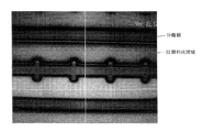
[実施例7]
図22は本発明のインクジェット方式を用いてEL層を形成した試料の顕微鏡写真を示す。試料の構造は、アクリル樹脂で形成した絶縁膜上にITOで形成した画素電極が設けられ、感光性アクリル樹脂で形成した分離層がストライプ状に設けられている。
【0215】
ITO上には最初に溶液塗布法(スピンコーティング法)でPEDOT層が形成される。そのとき、ITOは疎水性であるので、親水性とするため酸素プラズマ処理とCF4プラズマ処理を行っている。
【0216】
EL層はアニソール20mgにPPVを0.04gの割合で溶かしたものを用い、インクジェット方式により形成している。分離層の間隔は90μmであり、その間にEL層が連続的に形成されている様子が分かる。このようにして、EL層の形成を簡便でかつ高速に処理することが可能となっている。
【0217】
【発明の効果】
本発明を用いることで、EL層の形成を簡便でかつ高速に処理することが可能となる。また、EL素子が水分や熱によって劣化することを抑制することができる。また、EL層からアルカリ金属が拡散してTFT特性に悪影響を与えることを防ぐことができる。その結果、EL表示装置の動作性能や信頼性を大幅に向上させることができる。
【0218】
また、そのようなEL表示装置を表示ディスプレイとして有することで、画像品質が良く、耐久性のある(信頼性の高い)応用製品(電子装置)を生産することが可能となる。
【図面の簡単な説明】
【図1】 本発明のインクジェット方式でEL層を連続的に形成する概念を説明するための図。
【図2】 マトリクス状に配列した各画素電極に対し、EL層をストライプ状或いは連続的に形成する概念を説明するための図。
【図3】 インクジェット方式を説明するための図。
【図4】 本発明のインクジェット方式でEL層を連続的に形成する概念を説明するための図。
【図5】 EL表示装置の画素部の断面構造を示す図。
【図6】 EL表示装置の画素部の上面構造及び構成を示す図。
【図7】 アクティブマトリクス型EL表示装置の作製工程を示す図。
【図8】 アクティブマトリクス型EL表示装置の作製工程を示す図。
【図9】 アクティブマトリクス型EL表示装置の作製工程を示す図。
【図10】 ELモジュールの外観を示す図。
【図11】 EL表示装置の回路ブロック構成を示す図。
【図12】 EL表示装置の画素部を拡大した図。
【図13】 EL表示装置のサンプリング回路の素子構造を示す図。
【図14】 ELモジュールの示す上面図。
【図15】 EL表示装置の封止構造を示す断面図。
【図16】 パッシブ型EL表示装置の作製工程を示す図。
【図17】 EL表示装置を作製するための装置構成を説明する図。
【図18】 EL表示装置の画素部の断面構造を示す図。
【図19】 電子装置の具体例を示す図。
【図20】 電子装置の具体例を示す図。
【図21】 画素部の画素配列を説明する図。
【図22】 本発明のインクジェット方式でEL層を連続的に形成した試料の顕微鏡写真。[0001]
BACKGROUND OF THE INVENTION
The present invention includes an electro-optical device typified by an electroluminescence (EL) display device formed by fabricating a semiconductor element (an element using a semiconductor thin film) on a substrate, and the electro-optical device as a display display. The present invention relates to an electronic apparatus (electronic device). In particular, it relates to a manufacturing method thereof. In this specification, a layer including an organic compound from which electroluminescence is obtained is referred to as an EL layer. Minescence in an organic compound includes light emission (fluorescence) when returning from the singlet excited state to the ground state and light emission (phosphorescence) when returning from the triplet excited state to the ground state, and includes both.
[0002]
[Prior art]
In recent years, a technique for forming a thin film transistor (hereinafter referred to as TFT) on a substrate has greatly advanced, and application development to an active matrix display device has been advanced. In particular, a TFT using a semiconductor film having a crystal structure (for example, a polysilicon film) has higher field effect mobility than a TFT using a conventional amorphous silicon film, and thus can operate at high speed. Therefore, a driver circuit connected to the pixel portion can be formed using a TFT and formed over the same substrate.
[0003]
Such an active matrix display device has various advantages such as reduction in manufacturing cost by making various circuits and elements on the same substrate, downsizing and thinning of the display device, increase in yield, and improvement in throughput. Has been attracting attention as it can be obtained.
[0004]
In the active matrix EL display device, each pixel is provided with a switching element made of a TFT, and a driving element that controls current is operated by the switching element to cause the EL layer (light emitting layer) to emit light. For example, there is an EL display device described in US Pat. No. 5,684,365 (see Japanese Laid-Open Publication No. 8-234683) and Japanese Laid-Open Publication No. 10-189252.
[0005]
In these color display methods using an EL display device, an attempt is made to arrange an EL layer that emits three primary colors of red (R), green (G), and blue (B) for each pixel. However, most of the materials generally used for the EL layer are organic materials, and it has been difficult to apply the photolithography technique used in microfabrication as it is. The reason is that the EL material itself is very weak against moisture and is difficult to handle as it easily dissolves in the developer.
[0006]
As a technique for solving such a problem, a technique for forming an EL layer by an inkjet method has been proposed. For example, Japanese Patent Application Laid-Open No. 10-012377 discloses an active matrix EL display body in which an EL layer is formed by an ink jet method. A similar technique is also disclosed in “Multicolor Pixel Patterning of Light-Emitting Polymers by Ink-jet Printing; T. Shimada et.al., p376-379, SID 99 DIGEST”.
[0007]
[Problems to be solved by the invention]
In the inkjet method, an EL layer can be formed for each pixel, and a process of patterning after forming the EL layer can be omitted. However, in both an active matrix EL display device and a passive EL display device, higher position accuracy and higher processing speed are required as the screen size increases and the pixel density increases.
[0008]
An object of the present invention is to easily and rapidly process formation of an EL layer by an ink jet method. It is another object of the present invention to provide a method for manufacturing an electro-optical device with high operation performance and reliability, particularly a method for manufacturing an EL display device. An object of the present invention is to improve the quality of an electronic device (electronic device) having the electro-optical device as a display for display by improving the image quality of the electro-optical device.
[0009]
[Means for Solving the Problems]
In order to achieve the above object, in the present invention, when an EL layer is formed by an inkjet method, the EL layer is continuously provided over a plurality of pixels. Specifically, EL layers are continuously formed in stripes for a selected column or row for pixel electrodes arranged in a matrix of m rows and n columns. Alternatively, an EL layer is formed in an oval shape or a rectangular shape corresponding to each pixel electrode.
[0010]
In the ink jet method, a predetermined pattern is formed by repeatedly performing operations of ink head position control and ink discharge (a solution containing the material when forming an EL layer). However, as the screen size increases and the pixel density increases, the processing time becomes enormous in the method of forming the EL layer corresponding to each pixel electrode. However, in the method of forming the stripe shape, the oval shape, or the rectangular shape as described above, the EL layer can be formed by continuously scanning the ink head, and the processing time can be shortened.
[0011]
In order to manufacture an EL display device for color display, EL layers corresponding to red, green, and blue colors may be formed in a stripe shape, an oval shape, or a rectangular shape. Such an EL layer and a manufacturing method of the EL layer can be applied to either an active matrix type or a passive matrix type.
[0012]
Furthermore, in the present invention, alkali metal diffusion from an EL element formed by an ink jet method is prevented by an insulating film (passivation film) provided between the EL element and the TFT. Specifically, an insulating film that prevents permeation of alkali metal is provided over the planarization film that covers the TFT. That is, the insulating film having a sufficiently low alkali metal diffusion rate at the operating temperature of the EL display device may be used.
[0013]
Preferably, an insulating film that does not transmit moisture and alkali metal and has high thermal conductivity (high heat dissipation effect) is selected, and this insulating film is provided in contact with the EL element, or more preferably, such an insulating film is used. The EL element is surrounded by a film. That is, an insulating film that has a blocking effect on moisture and alkali metal and has a heat dissipation effect is provided at a position as close as possible to the EL element, and the deterioration of the EL element is suppressed by the insulating film.
[0014]
In the case where such an insulating film cannot be used as a single layer, an insulating film having a blocking effect on moisture and alkali metal and an insulating film having a heat dissipation effect can be stacked and used. Furthermore, an insulating film having a blocking effect on moisture, an insulating film having a blocking effect on alkali metal, and an insulating film having a heat dissipation effect can be stacked and used.
[0015]
DETAILED DESCRIPTION OF THE INVENTION
[Embodiment 1]
FIG. 1 is a diagram for explaining the concept of the present invention. FIG. 1A illustrates a structure in which a
[0016]
The
[0017]
FIG. 2 is a diagram illustrating details when an EL layer is formed in the pixel portion. In FIG. 2A, in the
[0018]
Alternatively, the
[0019]
FIG. 1B is a cross-sectional structure diagram of the conceptual diagram illustrated in FIG. 1A, and illustrates a state where the scan line
[0020]
FIG. 1C is a diagram for explaining the pixel portion in more detail. A
[0021]
FIG. 3 is a diagram illustrating the configuration of the ink head, and is an example in which a piezo method is adopted. FIG. 3A shows a piezoelectric element (piezoelectric element) 131, a
[0022]
FIG. 4 is also a diagram for explaining the concept of the present invention. The
[0023]
[Embodiment 2]
The active matrix EL display device of the present invention will be described with reference to FIGS. FIG. 5 is a cross-sectional view of a pixel of an active matrix EL display device according to the present invention, FIG. 6A is a top view thereof, and FIG. 6B is a circuit configuration thereof. Actually, a plurality of such pixels are arranged in a matrix to form a pixel portion (image display portion).
[0024]
Note that the cross-sectional view of FIG. 5 shows a cut surface cut along AA ′ in the top view shown in FIG. Here, since common reference numerals are used in FIGS. 5 and 6, it is preferable to refer to both drawings as appropriate.
[0025]
In FIG. 5, 11 is a substrate, and 12 is an insulating film (hereinafter referred to as a base film) serving as a base. As the
[0026]
The
[0027]
In addition, it is effective to dissipate the heat generated by the TFT by providing the
[0028]
Two TFTs are formed in the pixel.
[0029]
However, the switching TFT and the current control TFT need not be limited to the n-channel TFT, and a p-channel TFT can be used for both or one of them. In any case, the TFT may be selected depending on the polarity of the bias voltage applied to the EL element connected to the current control TFT.
[0030]
The switching
[0031]
Although not shown, the
[0032]
The active layer is formed of a semiconductor film including a crystal structure. That is, a single crystal semiconductor film, a polycrystalline semiconductor film, or a microcrystalline semiconductor film may be used. The
[0033]
Further, in the switching
[0034]
Note that it is more preferable to provide an offset region (a region made of a semiconductor layer having the same composition as the channel formation region to which no gate voltage is applied) between the channel formation region and the LDD region in order to reduce the off-state current value. In the case of a multi-gate structure having two or more gate electrodes, a high-concentration impurity region provided between channel formation regions is effective in reducing the off-current value.
[0035]
As described above, a switching element having a sufficiently low off-state current value can be realized by using a TFT having a multi-gate structure as the switching
[0036]
That is, it is possible to eliminate the capacitor that has been a factor for reducing the effective light emitting area, and it is possible to widen the effective light emitting area. This means that the image quality of the EL display device can be brightened.
[0037]
The
[0038]
As shown in FIG. 6, the drain of the switching TFT is connected to the gate of the current control TFT. Specifically, the
[0039]
The
[0040]
Note that the channel length L1 of the switching
[0041]
In the present invention, the channel lengths L1 and L2 and the channel widths W1 and W2 are not limited to specific numerical ranges, but W1 is 0.1 to 5 μm (typically 1 to 3 μm), and W2 is 0. The thickness is preferably 5 to 30 μm (typically 2 to 10 μm). At this time, L1 is preferably 0.2 to 18 μm (typically 2 to 15 μm), and L2 is preferably 0.1 to 50 μm (typically 1 to 20 μm).
[0042]
In the
[0043]
By setting these numerical ranges, all standards are covered, from EL display devices having the number of VGA class pixels (640 × 480) to EL display devices having the number of high-definition class pixels (1920 × 1080 or 1280 × 1024). be able to. The length (width) of the LDD region formed in the switching
[0044]
Further, in the EL display device shown in FIG. 5, in the
[0045]
The
[0046]
Regarding deterioration due to hot carrier injection, it is known that a structure in which an LDD region overlaps a gate electrode is very effective. However, if the entire LDD region is overlaid on the gate electrode, the off-current value increases. Therefore, the applicant has a novel structure in which LDD regions that do not overlap with the gate electrode are provided in series, thereby preventing hot carriers and off-current. It solves value measures at the same time.
[0047]
At this time, the length of the LDD region overlapping with the gate electrode may be 0.1 to 3 μm (preferably 0.3 to 1.5 μm). If it is too long, the parasitic capacitance is increased, and if it is too short, the effect of preventing hot carriers is weakened. The length of the LDD region that does not overlap with the gate electrode may be 1.0 to 3.5 μm (preferably 1.5 to 2.0 μm). If it is too long, it will not be possible to pass a sufficient current, and if it is too short, the effect of reducing the off-current value will be weak.
[0048]
Further, in the above structure, a parasitic capacitance is formed in a region where the gate electrode and the LDD region overlap with each other. Therefore, it is preferable not to provide between the
[0049]
Further, from the viewpoint of increasing the amount of current that can be passed, the thickness of the active layer (especially the channel formation region) of the
[0050]
The film thickness of the
[0051]
It is also effective to prevent thermal degradation of the EL layer by providing the
[0052]
As a translucent material that prevents alkali metal from passing through and has a heat dissipation effect, at least one element selected from B (boron), C (carbon), and N (nitrogen), Al (aluminum), Si ( And an insulating film containing at least one element selected from silicon and P (phosphorus). For example, aluminum nitride represented by aluminum nitride (AlxNy), silicon carbide represented by silicon carbide (SixCy), silicon nitride represented by silicon nitride (SixNy), and boron nitride (BxNy) Boron phosphide represented by boron nitride and boron phosphide (BxPy) can be used. In addition, an aluminum oxide typified by aluminum oxide (AlxOy) has excellent translucency and a thermal conductivity of 20 Wm. -1 K -1 It can be said that it is one of the preferable materials. These materials not only have the above effects, but also have an effect of preventing moisture from entering.
[0053]
Other elements can be combined with the above compound. For example, it is possible to use aluminum nitride oxide represented by AlNxOy by adding nitrogen to aluminum oxide. This material has not only a heat dissipation effect but also an effect of preventing moisture, alkali metal and the like from entering.
[0054]
Moreover, the material described in Unexamined-Japanese-Patent No. 62-90260 can be used. That is, an insulating film containing Si, Al, N, O, and M (where M is at least one of rare earth elements, preferably Ce (cerium), Yb (ytterbium), Sm (samarium), Er (erbium), Y ( Yttrium), La (lanthanum), Gd (gadolinium), Dy (dysprosium), and Nd (neodymium). These materials have not only a heat dissipation effect but also an effect of preventing intrusion of moisture, alkali metals, and the like.
[0055]
In addition, a carbon film including at least a diamond thin film or an amorphous carbon film (in particular, a material having characteristics close to diamond, called diamond-like carbon) can be used. These have very high thermal conductivity and are extremely effective as a heat dissipation layer. However, as the film thickness increases, the film becomes brownish and the transmittance decreases. Therefore, it is preferable to use the film as thin as possible (preferably 5 to 100 nm).
[0056]
Note that the purpose of the
[0057]
In addition, the EL display device can be roughly divided into four color display methods, a method of forming three types of EL elements corresponding to RGB, a method of combining a white light emitting EL element and a color filter, and blue or blue-green. There are a method in which a light-emitting EL element and a phosphor (fluorescent color conversion layer: CCM) are combined, and a method in which a transparent electrode is used as a cathode (counter electrode) and EL elements corresponding to RGB are stacked. Although only one pixel is shown in FIG. 5, pixels having the same structure are formed corresponding to the respective colors of red, green, and blue, so that color display can be performed. A known material may be used for the EL layers of these colors. However, the present invention can be carried out regardless of the light emission method, and all the above four methods can be used in the present invention.
[0058]
When the
[0059]
It is very important to flatten the step due to the TFT by the second
[0060]
The
[0061]
As described above, it is effective to planarize a TFT with an organic resin film in manufacturing an EL display device, but there has not been a structure that takes into account deterioration of an organic resin film due to heat generated in an EL element. It can be said that the present invention solves this problem by providing the
[0062]
The pixel electrode (EL element anode) 46 is a transparent conductive film, and a contact hole (opening) is formed in the
[0063]
When the
[0064]
After the
[0065]
Any known EL material can be used in the present invention. As a known material, an organic material is widely known, and it is preferable to use an organic material in consideration of a driving voltage. As the organic EL material, for example, materials disclosed in the following US patents or publications can be used.
[0066]
U.S. Patent No. 4,356,429, U.S. Patent No. 4,539,507, U.S. Patent No. 4,720,432, U.S. Patent No. 4,769,292, U.S. Patent No. 4,885,211, US Patent No. 4,950,950, US Patent No. 5,059,861, US Patent No. 5,047,687, US Patent No. 5,073,446, US Patent No. 5,059,862, US Pat. No. 5,061,617, US Pat. No. 5,151,629, US Pat. No. 5,294,869, US Pat. No. 5,294,870, JP-A-10-189525, JP-A-10-189525 JP-A-8-241048, JP-A-8-78159.
[0067]
Specifically, as the organic material for the hole injection layer, those represented by the following general formula can be used.
[0068]
[Chemical 1]
Where Q is N or C—R (carbon chain), M is a metal, metal oxide or metal halide, R is hydrogen, alkyl, aralkyl, allyl or alkaryl, T1, T2 are hydrogen, An unsaturated six-membered ring containing a substituent such as alkyl or halogen.
[0070]
An aromatic tertiary amine can be used as the organic material for the hole transport layer, and preferably includes tetraallyldiamine represented by the following general formula.
[0071]
[Chemical 2]
Where Are is an arylene group, n is an integer of 1 to 4, Ar, R 7 , R 8 , R 9 Are the selected allyl groups.
[0073]
In addition, a metal oxinoid compound can be used as the organic material for the EL layer, the electron transport layer, or the electron injection layer. What is necessary is just to use what is represented with the following general formulas as a metal oxinoid compound.
[0074]
[Chemical 3]
Where R 2 -R 7 Can be replaced, and the following metal oxinoid compounds can also be used.
[0076]
[Formula 4]
Where R 2 -R 7 Is as defined above, L 1 -L Five Is a group of carbohydrates containing 1 to 12 carbon elements and L 1 , L 2 Or L 2 , L Three Together can form a benzo ring. Moreover, the following metal oxinoid compounds may be used.
[0078]
[Chemical formula 5]
Where R 2 -R 6 Can be replaced. As described above, the organic EL material includes a coordination compound having an organic ligand. However, the above example is an example of the organic EL material that can be used as the EL material of the present invention, and it is not absolutely necessary to limit to this.
[0080]
In the present invention, since an ink jet method is used as a method for forming an EL layer, polymer materials are often used as preferable EL materials. Typical polymer materials include polymer materials such as polyparaphenylene vinylene (PPV) and polyfluorene. For colorization, for example, cyanopolyphenylene vinylene is preferable for the red light emitting material, polyphenylene vinylene is preferable for the green light emitting material, and polyphenylene vinylene and polyalkylphenylene are preferable for the blue light emitting material.
[0081]
However, the above example is an example of the organic EL material that can be used as the EL material of the present invention, and it is not absolutely necessary to limit to this. With respect to the organic EL material that can be used in the ink jet method, all materials described in JP-A-10-012377 can be cited.
[0082]
The ink jet method is roughly classified into a bubble jet method (also referred to as a thermal ink jet method) and a piezo method, but the piezo method is desirable for carrying out the present invention.
[0083]
In addition, the shape when the EL material is actually applied on the pixel electrode is formed in an oval shape or a rectangular shape by continuously forming a stripe shape or a plurality of dots as shown in the first embodiment. The
[0084]
In order to perform color display, as shown in FIG. 6, a red light emitting
[0085]
FIG. 21 illustrates a configuration of the pixel portion, and shows a state in which a plurality of pixel electrodes are formed in an EL layer formed in a stripe shape, an oval shape, or a rectangular shape. In FIG. 21A, a plurality of pixel electrodes are provided for
[0086]
FIG. 21B shows another configuration example. For example, a plurality of pixel electrodes are provided for
[0087]
Further, when forming the
[0088]
After the
[0089]
The
[0090]
Note that the
[0091]
The thickness of the
[0092]
Further, since the EL layer is vulnerable to heat as described above, it is desirable to form the film at as low a temperature as possible (preferably in a temperature range from room temperature to 120 ° C.). Therefore, the plasma CVD method, the sputtering method, the vacuum deposition method, the ion plating method, or the solution coating method (spin coating method) can be said to be a preferable film forming method.
[0093]
As described above, it is possible to sufficiently suppress the deterioration of the EL element only by providing the
[0094]
In addition, the EL display device of the present invention has a pixel portion composed of pixels having a structure as shown in FIG. 5, and TFTs having different structures are arranged in the pixels according to functions. As a result, a switching TFT having a sufficiently low off-current value and a current control TFT resistant to hot carrier injection can be formed in the same pixel, have high reliability, and can display a good image (operation) An EL display device with high performance is obtained.
[0095]
Although the multi-gate TFT is used as the switching TFT in the pixel structure of FIG. 5, the arrangement of the LDD region and the like need not be limited to those shown in FIG. The present invention having the above-described configuration will be described in more detail with the following examples.
[0096]
【Example】
[Example 1]
An embodiment of the present invention will be described with reference to FIGS. Here, a method for simultaneously manufacturing a TFT of a pixel portion and a driver circuit portion provided around the pixel portion will be described. However, in order to simplify the description, a CMOS circuit, which is a basic circuit, is illustrated with respect to the drive circuit.
[0097]
First, as shown in FIG. 7A, a
[0098]
In addition, it is effective to provide an insulating film made of the same material as that of the
[0099]
Next, an amorphous silicon film (not shown) having a thickness of 50 nm is formed on the
[0100]
Then, the amorphous silicon film is crystallized by a known technique to form a crystalline silicon film (also referred to as a polycrystalline silicon film or a polysilicon film) 302. Known crystallization methods include a thermal annealing method using an electric furnace, a laser annealing method using laser light, and a lamp annealing method using infrared light. In this embodiment, crystallization is performed by a laser annealing method using excimer laser light using XeCl gas.
[0101]
In this embodiment, a pulse oscillation type excimer laser beam processed into a linear shape is used. However, a rectangular shape, a continuous oscillation type argon laser beam, or a continuous oscillation type excimer laser beam may be used. . The light source of the laser light is not limited to the excimer laser, and the second harmonic or the third harmonic of the YAG laser may be used.
[0102]
In this embodiment, a crystalline silicon film is used as an active layer of a TFT, but an amorphous silicon film can also be used. However, since the current control TFT needs to pass a large current, it is advantageous to use a crystalline silicon film that easily allows a current to flow.
[0103]
It is effective to form the active layer of the switching TFT that needs to reduce the off current from an amorphous silicon film, and to form the active layer of the current control TFT from a crystalline silicon film. Since the amorphous silicon film has low carrier mobility, it is difficult for an electric current to flow and an off current is difficult to flow. That is, the advantages of both an amorphous silicon film that hardly allows current to flow and a crystalline silicon film that easily allows current to flow can be utilized.
[0104]
Next, as shown in FIG. 7B, a
[0105]
Then, resist
[0106]
In the n-
[0107]
Next, as shown in FIG. 7C, the
[0108]
By this step, the end portion of the n-
[0109]
Next, as shown in FIG. 7D, unnecessary portions of the crystalline silicon film are removed, and island-shaped semiconductor films (hereinafter referred to as active layers) 307 to 310 are formed.
[0110]
Next, as shown in FIG. 7E, a
[0111]
Next, a conductive film having a thickness of 200 to 400 nm is formed and patterned to form
[0112]
The gate electrode may be formed of a single-layer conductive film, but it is preferable to form a stacked film of two layers or three layers as necessary. Any known conductive film can be used as the material of the gate electrode. However, a material that can be finely processed as described above, specifically, that can be patterned to a line width of 2 μm or less is preferable.
[0113]
Typically, a film made of an element selected from tantalum (Ta), titanium (Ti), molybdenum (Mo), tungsten (W), chromium (Cr), conductive silicon (Si), or the element Nitride films (typically tantalum nitride films, tungsten nitride films, titanium nitride films), alloy films combining the above elements (typically Mo—W alloys, Mo—Ta alloys), or of the above elements A silicide film (typically a tungsten silicide film or a titanium silicide film) can be used. Of course, it may be used as a single layer or may be laminated. In this embodiment, a laminated film including a tantalum nitride (TaN) film having a thickness of 50 nm and a Ta film having a thickness of 350 nm is used. This may be formed by sputtering. Further, when an inert gas such as Xe or Ne is added as a sputtering gas, peeling of the film due to stress can be prevented.
[0114]
At this time, the
[0115]
Next, as shown in FIG. 8A, an n-type impurity element (phosphorus in this embodiment) is added in a self-aligning manner using the
[0116]
Next, as shown in FIG. 8B, resist
[0117]
In this step, the source region or drain region of the n-channel TFT is formed. However, in the switching TFT, a part of the n-
[0118]
Next, as shown in FIG. 8C, the resist
[0119]
Note that the
[0120]
Next, after removing the resist
[0121]
At this time, it is important to eliminate oxygen in the atmosphere as much as possible. This is because the presence of even a small amount of oxygen oxidizes the exposed surface of the gate electrode, which increases resistance and makes it difficult to make ohmic contact later. Therefore, the oxygen concentration in the treatment atmosphere in the activation step is 1 ppm or less, preferably 0.1 ppm or less.
[0122]
Next, when the activation process is completed, a
[0123]
With such a structure, the wiring resistance of the gate wiring can be extremely reduced, so that an image display region (pixel portion) having a large area can be formed. That is, the pixel structure of this embodiment is extremely effective in realizing an EL display device having a screen size of 10 inches or more (or 30 inches or more) diagonally.
[0124]
Next, as shown in FIG. 9A, a first
[0125]
Further, a hydrogenation treatment is performed by performing a heat treatment at 300 to 450 ° C. for 1 to 12 hours in an atmosphere containing 3 to 100% hydrogen. This step is a step in which the dangling bonds of the semiconductor film are terminated with hydrogen by thermally excited hydrogen. As another means of hydrogenation, plasma hydrogenation (using hydrogen excited by plasma) may be performed. The hydrogenation process may be performed while the first
[0126]
Next, contact holes are formed in the first
[0127]
Next, a
[0128]
Prior to the formation of the silicon nitride oxide film, H 2 , NH Three It is effective to perform plasma treatment using a gas containing isohydrogen. Hydrogen excited by this pretreatment is supplied to the first
[0129]
Next, a second
[0130]
Next, a
[0131]
Then, a contact hole reaching the
[0132]
In this embodiment, the
[0133]
Since the
[0134]
Next, as shown in FIG. 9C, an
[0135]
Note that the material described in Embodiment 2 can be used for the
[0136]
As the hole injection layer or the hole transport layer, an amine-based TPD (triphenylamine derivative) may be used. Besides, hydrazone (typically DEH), stilbene (typically STB), star A bust system (typically m-MTDATA) or the like can be used. In particular, a star bust material having a high glass transition temperature and being difficult to crystallize is preferable.
[0137]
As the light emitting layer, BPPC, perylene, and DCM can be used as the red light emitting layer, and in particular Eu (DBM). Three The Eu complex represented by (Phen) (detailed in J. Kido et.al, Appl. Phys., Vol. 35, pp. L394-396, 1996) has sharp emission at a wavelength of 620 nm and high monochromaticity.
[0138]
Moreover, as a green light emitting layer, typically, Alq Three (8-hydroxyquinoline alminium) to which a few mol% quinacridone or coumarin is added can be used. The chemical formula is as follows.
[0139]
[Chemical 6]
As the blue light-emitting layer, a distyarylene amine derivative obtained by adding amino-substituted DSA to DSA (distyryarylene derivative) can be typically used. In particular, it is preferable to use distyrylbiphenyl (DPVBi), which is a high-performance material. The chemical formula is as follows.
[0141]
[Chemical 7]
In addition, although the
[0143]
The
[0144]
Note that the thickness of the
[0145]
Thus, an active matrix EL display device having a structure as shown in FIG. 9C is completed. By the way, the active matrix EL display device of this embodiment can provide extremely high reliability and improve the operating characteristics by arranging TFTs having an optimal structure not only in the pixel portion but also in the drive circuit portion.
[0146]
First, a TFT having a structure that reduces hot carrier injection so as not to reduce the operating speed as much as possible is used as an n-channel TFT 205 of a CMOS circuit that forms a driving circuit. Note that the drive circuit here includes a shift register, a buffer, a level shifter, a sampling circuit (sample and hold circuit), and the like. In the case of performing digital driving, a signal conversion circuit such as a D / A converter may be included.
[0147]
In this embodiment, as shown in FIG. 9C, the active layer of the n-channel type 205 includes a
[0148]
The reason why the LDD region is formed only on the drain region side is to prevent the operation speed from being lowered. In addition, the n-channel TFT 205 does not need to care about the off-current value, and it is better to focus on the operation speed than that. Therefore, it is desirable that the
[0149]
In addition, since the p-channel TFT 206 of the CMOS circuit is hardly concerned about deterioration due to hot carrier injection, it is not particularly necessary to provide an LDD region. Needless to say, it is possible to provide an LDD region as in the case of the n-channel TFT 205 and take measures against hot carriers. Of the driving circuits, the sampling circuit is a little special compared to other circuits, and a large current flows bidirectionally in the channel formation region. That is, the roles of the source region and the drain region are interchanged. Furthermore, it is necessary to keep the off-current value as low as possible, and in that sense, it is desirable to dispose a TFT having an intermediate function between the switching TFT and the current control TFT.
[0150]
Therefore, it is desirable to dispose a TFT having a structure as shown in FIG. 13 as the n-channel TFT forming the sampling circuit. As shown in FIG. 13, part of the
[0151]
In addition, a pixel portion is formed by forming a pixel having a structure as shown in FIG. Since the structure of the switching TFT and the current control TFT formed in the pixel has already been described with reference to FIG. 5, the description thereof is omitted here.
[0152]
Actually, when completed up to FIG. 9C, packaging with a housing material such as a highly airtight protective film (laminate film, UV curable resin film, etc.) or ceramic sealing can so as not to be exposed to the outside air ( (Encapsulation) is preferable. At that time, the reliability (life) of the EL layer is improved by making the inside of the housing material an inert atmosphere or disposing a hygroscopic material (for example, barium oxide) inside.
[0153]
In addition, when the airtightness is improved by processing such as packaging, a connector (flexible printed circuit: FPC) for connecting the terminal routed from the element or circuit formed on the substrate and the external signal terminal is attached. Completed as a product. In this specification, an EL display device that can be shipped is referred to as an EL module.
[0154]
Here, the configuration of the active matrix EL display device of this embodiment will be described with reference to the perspective view of FIG. The active matrix EL display device of this embodiment includes a
[0155]
Further, the source side of the
[0156]
FIG. 11 shows an example of a circuit configuration of the EL display device shown in FIG. The circuit configuration in FIG. 11 is an example of analog driving, and includes a source side driver circuit 701, a gate side driver circuit (A) 707, a gate side driver circuit (B) 711, and a pixel portion 706. Note that in this specification, the drive circuit is a generic name including a source side processing circuit and a gate side drive circuit.
[0157]
The source side driver circuit 701 includes a shift register 702, a level shifter 703, a buffer 704, and a sampling circuit (sample and hold circuit) 705. The gate side driver circuit (A) 707 includes a
[0158]
Here, the shift registers 702 and 708 have a driving voltage of 5 to 16 V (typically 10 V), and an n-channel TFT used in a CMOS circuit forming the circuit has a structure indicated by 205 in FIG. Is suitable.
[0159]
The
[0160]
The above configuration can be easily realized by manufacturing a TFT according to the manufacturing steps shown in FIGS. In addition, in this embodiment, only the configuration of the pixel portion and the drive circuit is shown. However, according to the manufacturing process of this embodiment, other driving such as a signal dividing circuit, a D / A converter circuit, an operational amplifier circuit, and a γ correction circuit is performed. It is considered that logic circuits other than circuits can be formed on the same substrate, and further, a memory portion, a microprocessor, and the like can be formed.
[0161]
Further, the EL module of this embodiment including the housing material will be described with reference to FIGS. Note that the reference numerals used in FIGS. 10 and 11 are cited as necessary.
[0162]
In FIG. 14, 601 is a substrate, 602 is a pixel portion, 603 is a source side driver circuit, 604 is a gate side driver circuit, 612 is a
[0163]
Here, FIG. 15A shows a cross-sectional view taken along line AA ′ of FIG. 14 and FIG. 15B shows a cross-sectional view taken along line BB ′. 15A and 15B, the same reference numerals are used for the same portions as those in FIG.
[0164]
As shown in FIG. 15A, a
[0165]
The
[0166]
Further, a
[0167]
As the
[0168]
However, the
[0169]
Next, after the
[0170]
By encapsulating the EL element in the
[0171]
[Example 2]
In the first embodiment, an EL display device in which light emitted from an EL element is emitted to the substrate side on which a TFT is formed is shown. In this case, at least the region where the TFT is formed becomes a shadow, and the aperture ratio of the pixel portion is lowered accordingly. On the other hand, when the light emitted from the EL element is emitted upward (on the opposite side of the substrate on which the TFT is formed), it is easy to improve at least the aperture ratio.
[0172]
FIG. 18 shows a configuration of an EL display element that emits light upward. The configurations of the switching
[0173]
A cathode
[0174]
The
[0175]
[Example 3]
The method for manufacturing an EL layer by the inkjet method of the present invention and the manufactured EL layer can also be applied to a passive EL display device. The embodiment will be described with reference to FIG.
[0176]
In FIG. 16A, a
[0177]
The EL layer is used in a single layer or a stacked structure. The laminated structure is formed by a laminated structure in which a light emitting layer, an electron transport layer, an electron injection layer, a hole injection layer, or a hole transport layer are combined. In this embodiment, the hole injection layer and the light emitting layer are laminated. The structure is formed. First, as shown in FIG. 16B, a
[0178]
As shown in FIG. 16C, the light emitting layer is also formed by an ink jet method. In the case of performing color display, an ink head having cylinders of red, green, and blue colors is used, and an
[0179]
The cathode material is formed of a material such as MgAg (a material in which Mg and Ag are mixed at Mg: Ag = 10: 1), MgAgAl, LiAl, LiFAl, or the like. This cathode material is typically formed with a thickness of 1 to 50 nm by vacuum deposition. Further, Al or the like is laminated thereon as an auxiliary electrode. The cathode layer 1610 in FIG. 16D has such a structure, and is formed in a strip shape using a mask member when forming each film. The cathode layer 1610 formed in a strip shape is formed so as to be substantially orthogonal to the
[0180]
Since the material for forming the EL layer shown here is vulnerable to moisture, moisture, and the like, it is desirable to seal with a housing material. The material of the
[0181]
The material of the adhesive 1612 that bonds the
[0182]
[Example 4]
An example of a thin film forming apparatus for forming an EL element is shown in FIG. FIG. 17 shows a polymer organic EL layer as a light emitting layer, a metal film containing an element belonging to
[0183]
In FIG. 17, reference numeral 401 denotes a transfer chamber for loading or unloading substrates, which is also called a load / unload chamber. A carrier 402 on which a substrate is set is disposed here. It should be noted that the transfer chamber 401 may be distinguished from substrate carry-in and substrate carry-out. Reference numeral 403 denotes a common chamber including a mechanism (hereinafter referred to as a transport mechanism) 405 for transporting the substrate 404. A robot arm or the like that handles the substrate is a kind of the transport mechanism (1) 405.
[0184]
A plurality of processing chambers are connected to the common chamber 403 through
[0185]
It is possible to perform processing under vacuum by providing an exhaust pump in each processing chamber that performs a predetermined operation under reduced pressure. As the exhaust pump, an oil rotary pump, a mechanical booster pump, a turbo molecular pump, or a cryopump can be used, but a cryopump effective for removing water is preferable.
[0186]
The EL layer formed of a light emitting layer or an injection layer is formed in the ink jet printing processing chamber 415 or the spin coating processing chamber 408. The ink jet printing processing chamber 415 is provided with a substrate holding means, the ink head described with reference to FIG. Further, as described above, since the organic EL material is extremely sensitive to moisture, the inkjet printing processing chamber 415 and the spin coating processing chamber 408 are always kept in an inert atmosphere.
[0187]
In transferring the substrate, first, the evacuation processing chamber 412 is depressurized to the same pressure as the common chamber 403, and in that state, the
[0188]
In the present invention, the organic EL layer is formed by an ink jet method, but a light emitting layer is formed by an ink jet method, and some layers such as a hole or electron injection layer or a hole or electron transport layer are formed by a spin coat method. It may be formed by properly combining the two, such as forming.
[0189]
When the EL layer formation step is completed, the gate 413 is opened, the substrate is transferred to the processing chamber 412 for evacuation, and evacuation is performed with the gate 413 and the
[0190]
Note that although the firing processing chamber 409 is provided here, the firing step may be performed so that the susceptor of the vacuum exhaust processing chamber 412 can be heated. Degassing can be suppressed by evacuation after firing.
[0191]
In the first film formation chamber 410, a cathode is formed. As the cathode material, a known material is used. The cathode is formed by a vacuum deposition method. At that time, the substrate surface (the surface on which the polymer EL layer is formed) may be upward (face-up method) or downward (face-down method).
[0192]
In the case of the face-up method, the substrate transferred from the common chamber 403 is simply installed on the susceptor as it is, which is very simple. In the case of the face-down method, the transport mechanism (1) 405 or the first film formation processing chamber 410 needs to be provided with a mechanism for inverting the substrate. The advantage of less is obtained.
[0193]
In addition, when performing a vapor deposition process in the 1st film-forming
[0194]
The second deposition process chamber 411 is a process chamber for forming electrodes by a vapor deposition method. Here, an auxiliary electrode for assisting the cathode is formed. Further, a vapor deposition method or a sputtering method is used, but the vapor deposition method is preferable because it is less likely to cause damage. In any case, the common chamber 403 is cut off by the
[0195]
A metal film often used as a cathode is a metal film containing an element belonging to
[0196]
Next, the third film formation processing chamber 407 is a processing chamber for forming a third passivation film. As the third passivation film, a silicon nitride film, a silicon nitride oxide film, or the like is formed by a plasma CVD method. Therefore, although not shown, SiH Four , N 2 O, NH Three A gas supply system such as a plasma generating means using a high frequency power source of 13.56-60 MHz, a substrate heating means, and the like are provided. Since an EL layer made of an organic material is vulnerable to moisture or moisture, it is preferable to continuously provide such a passivation film without exposing it to the air atmosphere after the EL layer is formed.
[0197]
The greatest feature of the thin film forming apparatus having the above configuration is that it is performed by an ink jet method for forming an EL layer, and the means for that purpose is mounted on a multi-chamber type thin film forming apparatus together with a means for forming a cathode. It is in. Therefore, it is possible to start from the step of oxidizing the surface of the anode made of the transparent conductive film to the step of forming the auxiliary electrode without being exposed to the outside air. As a result, it is possible to form a polymer EL layer that is resistant to deterioration by simple means, and a highly reliable EL display device can be manufactured.
[0198]
[Example 5]
In the first embodiment, laser crystallization is used as a means for forming the
[0199]
In this embodiment, after an amorphous silicon film is formed, crystallization is performed using the technique described in Japanese Patent Laid-Open No. 7-130652. The technique described in this publication is a technique for obtaining a crystalline silicon film having high crystallinity by using an element such as nickel as a catalyst for promoting (promoting) crystallization.
[0200]
Further, after the crystallization step is completed, a step of removing the catalyst used for crystallization may be performed. In that case, the catalyst may be gettered by the technique described in JP-A-10-270363 or JP-A-8-330602. Further, a TFT may be formed using the technique described in the application specification of Japanese Patent Application No. 11-076967 by the present applicant.
[0201]
As described above, the manufacturing process described in Example 1 is one example, and other manufacturing processes can be used as long as the structure of FIG. 5 or FIG. 9C of Example 1 can be realized. No problem. In addition, the structure of a present Example can be freely combined with any structure of Embodiment 2 and Examples 1-2.
[0202]
[Example 6]
An active matrix EL display device or a passive EL display device (EL module) formed by implementing the present invention is a self-luminous type, and thus has better visibility in a bright place than a liquid crystal display device. Therefore, the application is wide as a direct-view type EL display device (referring to a display device incorporating an EL module).
[0203]
Note that one of the advantages of the EL display device over the liquid crystal display device is a wide viewing angle. Therefore, in order to watch TV broadcasts or the like on a large screen, the EL display device of the present invention may be used as a display device (display monitor) having a diagonal of 30 inches or more (typically 40 inches or more).
[0204]
Moreover, it can be used not only as an EL display device (a personal computer monitor, a TV broadcast reception monitor, an advertisement display monitor, etc.) but also as a display device for various electronic devices. Such electronic devices include video cameras, digital cameras, goggle-type displays (head-mounted displays), car navigation systems, personal computers, personal digital assistants (such as mobile computers, mobile phones or electronic books), and images with recording media. A playback device (specifically, a device provided with a display capable of playing back a recording medium such as a compact disc (CD), a laser disc (LD), or a digital video disc (DVD) and displaying an image thereof). Examples of these semiconductor devices are shown in FIGS.
[0205]
FIG. 19A illustrates an EL display, which includes a
[0206]
FIG. 19B illustrates a video camera, which includes a main body 2101, a display portion 2102, an
[0207]
FIG. 19C illustrates a head-mounted display, which includes a main body 2201, a signal cable 2202, a fixed
[0208]
FIG. 19D shows an image reproducing apparatus (specifically, a DVD reproducing apparatus) provided with a recording medium, which includes a main body 2301, a recording medium (CD, LD, DVD, etc.) 2302, an
[0209]
FIG. 19E illustrates a portable (mobile) computer, which includes a
[0210]
FIG. 19F illustrates a personal computer, which includes a main body 2501, a display portion 2503, a
[0211]
FIG. 20A illustrates a mobile phone, which includes a
[0212]
FIG. 20B illustrates an on-vehicle audio device, which includes a
[0213]
As described above, the application range of the present invention is extremely wide and can be applied to electronic devices in various fields. Moreover, the electronic apparatus of a present Example is realizable even if it uses the structure which consists of what combination of Examples 1-5.
[0214]
[Example 7]
FIG. 22 shows a micrograph of a sample in which an EL layer is formed using the ink jet system of the present invention. In the structure of the sample, pixel electrodes made of ITO are provided on an insulating film made of acrylic resin, and separation layers made of photosensitive acrylic resin are provided in stripes.
[0215]
A PEDOT layer is first formed on ITO by a solution coating method (spin coating method). At that time, since ITO is hydrophobic, oxygen plasma treatment and CF Four Plasma treatment is performed.
[0216]
The EL layer is formed by an inkjet method using 20 mg of anisole and PPV dissolved at a ratio of 0.04 g. The interval between the separation layers is 90 μm, and it can be seen that the EL layers are continuously formed therebetween. In this way, the formation of the EL layer can be processed easily and at high speed.
[0217]
【The invention's effect】
By using the present invention, the EL layer can be formed easily and at high speed. In addition, the EL element can be prevented from being deteriorated by moisture or heat. Further, it is possible to prevent the alkali metal from diffusing from the EL layer and adversely affecting the TFT characteristics. As a result, the operation performance and reliability of the EL display device can be greatly improved.
[0218]
In addition, by having such an EL display device as a display display, it is possible to produce an application product (electronic device) having good image quality and durability (high reliability).
[Brief description of the drawings]
FIG. 1 is a view for explaining a concept of continuously forming an EL layer by an ink jet method of the present invention.
FIG. 2 is a diagram for explaining a concept of forming an EL layer in a stripe shape or continuously for each pixel electrode arranged in a matrix.
FIG. 3 is a diagram for explaining an ink jet method.
FIG. 4 is a view for explaining the concept of continuously forming an EL layer by the inkjet method of the present invention.
FIG. 5 illustrates a cross-sectional structure of a pixel portion of an EL display device.
FIGS. 6A and 6B illustrate a top structure and a structure of a pixel portion of an EL display device. FIGS.
FIGS. 7A to 7C illustrate a manufacturing process of an active matrix EL display device. FIGS.
FIG. 8 illustrates a manufacturing process of an active matrix EL display device.
FIG. 9 illustrates a manufacturing process of an active matrix EL display device.
FIG. 10 is a diagram showing the appearance of an EL module.
FIG. 11 is a diagram showing a circuit block configuration of an EL display device.
FIG. 12 is an enlarged view of a pixel portion of an EL display device.
FIG. 13 is a diagram showing an element structure of a sampling circuit of an EL display device.
FIG. 14 is a top view showing an EL module.
FIG. 15 is a cross-sectional view illustrating a sealing structure of an EL display device.
FIG. 16 illustrates a manufacturing process of a passive EL display device.
FIGS. 17A and 17B illustrate a device structure for manufacturing an EL display device. FIGS.
FIG 18 illustrates a cross-sectional structure of a pixel portion of an EL display device.
FIG. 19 illustrates a specific example of an electronic device.
FIG. 20 illustrates a specific example of an electronic device.
FIG. 21 is a diagram illustrating a pixel arrangement of a pixel portion.
FIG. 22 is a micrograph of a sample in which an EL layer is continuously formed by the inkjet method of the present invention.
Claims (2)
前記画素部及び駆動回路部上に酸化アルミニウム又は窒化酸化アルミニウムからなる第3の絶縁膜を形成し、
前記第3の絶縁膜上に有機樹脂膜を形成し、
前記有機樹脂膜上に接して酸化アルミニウム又は窒化酸化アルミニウムからなる第1の絶縁膜を形成し、
前記第1の絶縁膜上に接してマトリクス状に配列された複数の第1の電極を形成し、
前記マトリクスの列毎又は行毎に一方向にインクヘッドを連続的に走査させながら、前記インクヘッドからインクドットを連続させて吐出することによって、前記マトリクスの列毎又は行毎にストライプ状のEL層を形成し、
前記EL層上に第2の電極を形成し、
前記第2の電極上に接してアルミニウム若しくは銀を含む材料からなる補助電極を形成し、
前記補助電極上に接して酸化アルミニウム又は窒化酸化アルミニウムからなる第2の絶縁膜を形成し、
前記駆動回路部には、nチャネル型TFTとpチャネル型TFTとを有するCMOS回路が複数設けられており、
サンプリング回路以外の前記CMOS回路において、nチャネル型TFTにはゲート電極のみと重なるLDD領域がドレイン領域側のみに設けられており、pチャネル型TFTにはLDD領域が設けられておらず、
前記サンプリング回路に用いられる前記CMOS回路において、nチャネル型TFTにはゲート電極に重なる領域と重ならない領域の双方を有するLDD領域がドレイン領域側及びソース領域側の双方に設けられており、pチャネル型TFTにはLDD領域が設けられていないことを特徴とする電気光学装置の作製方法。 Forming a pixel portion and a drive circuit portion in which a plurality of TFTs are formed;
Forming a third insulating film made of aluminum oxide or aluminum nitride oxide on the pixel portion and the drive circuit portion;
Forming an organic resin film on the third insulating film;
Forming a first insulating film made of aluminum oxide or aluminum nitride oxide in contact with the organic resin film;
Forming a plurality of first electrodes arranged in a matrix in contact with the first insulating film;
By continuously ejecting ink dots from the ink head while continuously scanning the ink head in one direction for each column or row of the matrix, a striped EL for each column or row of the matrix Forming a layer,
Forming a second electrode on the EL layer;
Forming an auxiliary electrode made of a material containing aluminum or silver in contact with the second electrode;
Forming a second insulating film made of aluminum oxide or aluminum nitride oxide in contact with the auxiliary electrode;
The driving circuit section is provided with a plurality of CMOS circuits having an n-channel TFT and a p-channel TFT,
In the CMOS circuit other than the sampling circuit, the n-channel type TFT has an LDD region overlapping the only gate electrode is provided on only the drain region side, not provided with an LDD region in the p-channel type TFT,
In the CMOS circuit used for the sampling circuit, the n-channel type TFT is provided in both LDD region on the drain region side and a source region side having both a region which does not overlap with the region overlapping the gate electrode, p-channel A manufacturing method of an electro-optical device, wherein an LDD region is not provided in a type TFT.
前記画素部及び駆動回路部上に酸化アルミニウム又は窒化酸化アルミニウムからなる第3の絶縁膜を形成し、
前記第3の絶縁膜上に有機樹脂膜を形成し、
前記有機樹脂膜上に接して酸化アルミニウム又は窒化酸化アルミニウムからなる第1の絶縁膜を形成し、
前記第1の絶縁膜上に接してマトリクス状に配列された複数の第1の電極を形成し、
前記マトリクスの列毎又は行毎に一方向にインクヘッドを連続的に走査させながら、前記インクヘッドからインクドットを連続させて吐出することによって、前記マトリクスの列毎又は行毎に前記第1の電極の各々に対応する長円形或いは長方形の複数のEL層を形成し、
前記EL層上に第2の電極を形成し、
前記第2の電極上に接してアルミニウム若しくは銀を含む材料からなる補助電極を形成し、
前記補助電極上に接して酸化アルミニウム又は窒化酸化アルミニウムからなる第2の絶縁膜を形成し、
前記駆動回路部には、nチャネル型TFTとpチャネル型TFTとを有するCMOS回路が複数設けられており、
サンプリング回路以外の前記CMOS回路において、nチャネル型TFTにはゲート電極のみと重なるLDD領域がドレイン領域側のみに設けられており、pチャネル型TFTにはLDD領域が設けられておらず、
前記サンプリング回路に用いられる前記CMOS回路において、nチャネル型TFTにはゲート電極に重なる領域と重ならない領域の双方を有するLDD領域がドレイン領域側及びソース領域側の双方に設けられており、pチャネル型TFTにはLDD領域が設けられていないことを特徴とする電気光学装置の作製方法。 Forming a pixel portion and a drive circuit portion in which a plurality of TFTs are formed;
Forming a third insulating film made of aluminum oxide or aluminum nitride oxide on the pixel portion and the drive circuit portion;
Forming an organic resin film on the third insulating film;
Forming a first insulating film made of aluminum oxide or aluminum nitride oxide in contact with the organic resin film;
Forming a plurality of first electrodes arranged in a matrix in contact with the first insulating film;
By continuously ejecting ink dots from the ink head while continuously scanning the ink head in one direction for each column or row of the matrix, the first for each column or row of the matrix. Forming a plurality of oval or rectangular EL layers corresponding to each of the electrodes;
Forming a second electrode on the EL layer;
Forming an auxiliary electrode made of a material containing aluminum or silver in contact with the second electrode;
Forming a second insulating film made of aluminum oxide or aluminum nitride oxide in contact with the auxiliary electrode;
The driving circuit section is provided with a plurality of CMOS circuits having an n-channel TFT and a p-channel TFT,
In the CMOS circuit other than the sampling circuit, the n-channel type TFT has an LDD region overlapping the only gate electrode is provided on only the drain region side, not provided with an LDD region in the p-channel type TFT,
In the CMOS circuit used for the sampling circuit, the n-channel type TFT is provided in both LDD region on the drain region side and a source region side having both a region which does not overlap with the region overlapping the gate electrode, p-channel A manufacturing method of an electro-optical device, wherein an LDD region is not provided in a type TFT.
Priority Applications (1)
| Application Number | Priority Date | Filing Date | Title |
|---|---|---|---|
| JP2000308742A JP4780826B2 (en) | 1999-10-12 | 2000-10-10 | Method for manufacturing electro-optical device |
Applications Claiming Priority (4)
| Application Number | Priority Date | Filing Date | Title |
|---|---|---|---|
| JP29031499 | 1999-10-12 | ||
| JP1999290314 | 1999-10-12 | ||
| JP11-290314 | 1999-10-12 | ||
| JP2000308742A JP4780826B2 (en) | 1999-10-12 | 2000-10-10 | Method for manufacturing electro-optical device |
Publications (3)
| Publication Number | Publication Date |
|---|---|
| JP2001185354A JP2001185354A (en) | 2001-07-06 |
| JP2001185354A5 JP2001185354A5 (en) | 2007-11-08 |
| JP4780826B2 true JP4780826B2 (en) | 2011-09-28 |
Family
ID=26557995
Family Applications (1)
| Application Number | Title | Priority Date | Filing Date |
|---|---|---|---|
| JP2000308742A Expired - Lifetime JP4780826B2 (en) | 1999-10-12 | 2000-10-10 | Method for manufacturing electro-optical device |
Country Status (1)
| Country | Link |
|---|---|
| JP (1) | JP4780826B2 (en) |
Families Citing this family (39)
| Publication number | Priority date | Publication date | Assignee | Title |
|---|---|---|---|---|
| JP4789341B2 (en) * | 2001-03-30 | 2011-10-12 | 三洋電機株式会社 | Semiconductor device and mask for manufacturing semiconductor device |
| US7211828B2 (en) | 2001-06-20 | 2007-05-01 | Semiconductor Energy Laboratory Co., Ltd. | Light emitting device and electronic apparatus |
| TW548860B (en) | 2001-06-20 | 2003-08-21 | Semiconductor Energy Lab | Light emitting device and method of manufacturing the same |
| JP5202673B2 (en) * | 2001-07-27 | 2013-06-05 | 株式会社半導体エネルギー研究所 | Method for manufacturing semiconductor device |
| US7488986B2 (en) * | 2001-10-26 | 2009-02-10 | Semiconductor Energy Laboratory Co., Ltd. | Light emitting device |
| JP3825395B2 (en) * | 2001-10-30 | 2006-09-27 | 株式会社半導体エネルギー研究所 | Light emitting device and electric appliance |
| US6956240B2 (en) | 2001-10-30 | 2005-10-18 | Semiconductor Energy Laboratory Co., Ltd. | Light emitting device |
| US7483001B2 (en) | 2001-11-21 | 2009-01-27 | Seiko Epson Corporation | Active matrix substrate, electro-optical device, and electronic device |
| TWI264121B (en) * | 2001-11-30 | 2006-10-11 | Semiconductor Energy Lab | A display device, a method of manufacturing a semiconductor device, and a method of manufacturing a display device |
| SG143063A1 (en) * | 2002-01-24 | 2008-06-27 | Semiconductor Energy Lab | Light emitting device and method of manufacturing the same |
| JP2003264067A (en) * | 2002-03-07 | 2003-09-19 | Ricoh Co Ltd | Functional element substrate, manufacturing installation of the same, image display device, and image display system |
| JP4481292B2 (en) * | 2002-03-13 | 2010-06-16 | 株式会社リコー | Functional element substrate manufacturing apparatus and method |
| US7148508B2 (en) | 2002-03-20 | 2006-12-12 | Seiko Epson Corporation | Wiring substrate, electronic device, electro-optical device, and electronic apparatus |
| JP4217428B2 (en) | 2002-05-31 | 2009-02-04 | キヤノン株式会社 | Display device |
| CN1729719B (en) * | 2002-12-19 | 2010-09-15 | 株式会社半导体能源研究所 | Display unit and method of fabricating display unit |
| JP2005032704A (en) * | 2003-06-18 | 2005-02-03 | Sharp Corp | Display element and display device |
| WO2005031798A2 (en) | 2003-09-26 | 2005-04-07 | Semiconductor Energy Laboratory Co., Ltd. | Light-emitting device and method for manufacturing the same |
| EP2276088B1 (en) | 2003-10-03 | 2018-02-14 | Semiconductor Energy Laboratory Co, Ltd. | Light emitting element, and light emitting device using the light emitting element |
| US8796670B2 (en) | 2003-12-26 | 2014-08-05 | Semiconductor Energy Laboratory Co., Ltd. | Light-emitting element |
| JP2006295104A (en) | 2004-07-23 | 2006-10-26 | Semiconductor Energy Lab Co Ltd | Light emitting element and light emitting device using the same |
| WO2006046678A1 (en) | 2004-10-29 | 2006-05-04 | Semiconductor Energy Laboratory Co., Ltd. | Composite material, light-emittintg element, light-emitting device, and manufacturing method thereof |
| JP2006201423A (en) | 2005-01-20 | 2006-08-03 | Seiko Epson Corp | Substrate with color element, film forming method, electro-optical device and electronic appliance |
| EP1866984B1 (en) | 2005-03-23 | 2017-08-30 | Semiconductor Energy Laboratory Co., Ltd. | Composite material, light emitting element and light emitting device |
| US7851989B2 (en) | 2005-03-25 | 2010-12-14 | Semiconductor Energy Laboratory Co., Ltd. | Light emitting device |
| EP1724852A3 (en) | 2005-05-20 | 2010-01-27 | Semiconductor Energy Laboratory Co., Ltd. | Light emitting element, light emitting device, and electronic device |
| JP4613700B2 (en) * | 2005-06-01 | 2011-01-19 | セイコーエプソン株式会社 | Electro-optical device and electronic apparatus |
| JP2006344545A (en) * | 2005-06-10 | 2006-12-21 | Toppan Printing Co Ltd | Method of manufacturing organic el element, and organic el element |
| US8017252B2 (en) | 2005-06-22 | 2011-09-13 | Semiconductor Energy Laboratory Co., Ltd. | Light emitting device and electronic appliance using the same |
| US7745989B2 (en) | 2005-06-30 | 2010-06-29 | Semiconductor Energy Laboratory Co., Ltd | Light emitting element, light emitting device, and electronic apparatus |
| JP5024021B2 (en) | 2007-12-18 | 2012-09-12 | セイコーエプソン株式会社 | LIGHT EMITTING DEVICE AND ELECTRONIC DEVICE |
| JP4650495B2 (en) * | 2008-02-05 | 2011-03-16 | セイコーエプソン株式会社 | LIGHT EMITTING DEVICE AND ELECTRONIC DEVICE |
| JP2010153365A (en) | 2008-11-19 | 2010-07-08 | Semiconductor Energy Lab Co Ltd | Light-emitting element, light-emitting device, electronic equipment, and illumination device |
| US8093803B2 (en) | 2009-03-17 | 2012-01-10 | Seiko Epson Corporation | Electro-optical device, electronic device, and method for manufacturing electro-optical device |
| KR101613865B1 (en) * | 2009-03-26 | 2016-04-20 | 가부시키가이샤 한도오따이 에네루기 켄큐쇼 | Light-emitting device and method for manufacturing the same |
| US8404500B2 (en) | 2009-11-02 | 2013-03-26 | Semiconductor Energy Laboratory Co., Ltd. | Method for manufacturing light-emitting element, light-emitting element, light-emitting device, lighting device, and electronic appliance |
| JP5969216B2 (en) | 2011-02-11 | 2016-08-17 | 株式会社半導体エネルギー研究所 | Light emitting element, display device, lighting device, and manufacturing method thereof |
| JP2017188478A (en) * | 2017-06-19 | 2017-10-12 | 株式会社半導体エネルギー研究所 | Light-emitting device |
| JP2019149384A (en) * | 2019-05-29 | 2019-09-05 | 株式会社半導体エネルギー研究所 | Light-emitting device |
| CN117813915A (en) | 2021-08-12 | 2024-04-02 | 株式会社半导体能源研究所 | Display device and method for manufacturing display device |
Family Cites Families (13)
| Publication number | Priority date | Publication date | Assignee | Title |
|---|---|---|---|---|
| JP3180978B2 (en) * | 1992-01-21 | 2001-07-03 | 京セラ株式会社 | Magneto-optical recording element |
| JPH05315360A (en) * | 1992-05-08 | 1993-11-26 | Fuji Xerox Co Ltd | Manufacture of thin film transistor |
| JP2677167B2 (en) * | 1993-07-08 | 1997-11-17 | 日本電気株式会社 | Method for manufacturing liquid crystal display device with built-in drive circuit |
| TW345654B (en) * | 1995-02-15 | 1998-11-21 | Handotai Energy Kenkyusho Kk | Active matrix display device |
| JP3111024B2 (en) * | 1995-07-19 | 2000-11-20 | キヤノン株式会社 | Apparatus and method for manufacturing color filter, method for manufacturing display apparatus, and method for manufacturing apparatus provided with display apparatus |
| JP3383535B2 (en) * | 1995-12-14 | 2003-03-04 | 株式会社半導体エネルギー研究所 | Semiconductor device |
| EP1367431B1 (en) * | 1996-09-19 | 2005-12-28 | Seiko Epson Corporation | Manufacturing method of a matrix type display device |
| JPH10107266A (en) * | 1996-09-27 | 1998-04-24 | New Japan Radio Co Ltd | Manufacture of mosfet |
| JPH10275682A (en) * | 1997-02-03 | 1998-10-13 | Nec Corp | Organic el element |
| JP3830238B2 (en) * | 1997-08-29 | 2006-10-04 | セイコーエプソン株式会社 | Active matrix type device |
| JPH11231805A (en) * | 1998-02-10 | 1999-08-27 | Sanyo Electric Co Ltd | Display device |
| CN100550472C (en) * | 1998-03-17 | 2009-10-14 | 精工爱普生株式会社 | The substrate of patterning thin film and surface treatment thereof |
| JPH11273855A (en) * | 1998-03-25 | 1999-10-08 | Tdk Corp | Organic el display device |
-
2000
- 2000-10-10 JP JP2000308742A patent/JP4780826B2/en not_active Expired - Lifetime
Also Published As
| Publication number | Publication date |
|---|---|
| JP2001185354A (en) | 2001-07-06 |
Similar Documents
| Publication | Publication Date | Title |
|---|---|---|
| JP4780826B2 (en) | Method for manufacturing electro-optical device | |
| KR100713032B1 (en) | An electro-optical device | |
| JP4730994B2 (en) | Electro-optical device, manufacturing method thereof, and electronic device | |
| KR100707887B1 (en) | Display device | |
| JP4776792B2 (en) | Light emitting device and electric appliance | |
| KR100733900B1 (en) | A light emitting device | |
| JP3904807B2 (en) | Display device | |
| JP4408118B2 (en) | Display device | |
| JP4515349B2 (en) | Electro-optic device | |
| JP4094437B2 (en) | Method for manufacturing electro-optical device | |
| JP4265818B2 (en) | Electro-optic device | |
| JP4532452B2 (en) | Electro-optic device | |
| JP2006011454A (en) | Electro-optical device and electronic device | |
| JP4515469B2 (en) | Method for manufacturing electro-optical device | |
| JP4532453B2 (en) | Method for manufacturing electro-optical device |
Legal Events
| Date | Code | Title | Description |
|---|---|---|---|
| A521 | Request for written amendment filed |
Free format text: JAPANESE INTERMEDIATE CODE: A523 Effective date: 20070920 |
|
| A621 | Written request for application examination |
Free format text: JAPANESE INTERMEDIATE CODE: A621 Effective date: 20070920 |
|
| A131 | Notification of reasons for refusal |
Free format text: JAPANESE INTERMEDIATE CODE: A131 Effective date: 20100316 |
|
| A521 | Request for written amendment filed |
Free format text: JAPANESE INTERMEDIATE CODE: A523 Effective date: 20100329 |
|
| A02 | Decision of refusal |
Free format text: JAPANESE INTERMEDIATE CODE: A02 Effective date: 20110329 |
|
| A521 | Request for written amendment filed |
Free format text: JAPANESE INTERMEDIATE CODE: A523 Effective date: 20110407 |
|
| A911 | Transfer to examiner for re-examination before appeal (zenchi) |
Free format text: JAPANESE INTERMEDIATE CODE: A911 Effective date: 20110531 |
|
| TRDD | Decision of grant or rejection written | ||
| A01 | Written decision to grant a patent or to grant a registration (utility model) |
Free format text: JAPANESE INTERMEDIATE CODE: A01 Effective date: 20110628 |
|
| A01 | Written decision to grant a patent or to grant a registration (utility model) |
Free format text: JAPANESE INTERMEDIATE CODE: A01 |
|
| A61 | First payment of annual fees (during grant procedure) |
Free format text: JAPANESE INTERMEDIATE CODE: A61 Effective date: 20110705 |
|
| FPAY | Renewal fee payment (event date is renewal date of database) |
Free format text: PAYMENT UNTIL: 20140715 Year of fee payment: 3 |
|
| R150 | Certificate of patent or registration of utility model |
Free format text: JAPANESE INTERMEDIATE CODE: R150 Ref document number: 4780826 Country of ref document: JP Free format text: JAPANESE INTERMEDIATE CODE: R150 |
|
| FPAY | Renewal fee payment (event date is renewal date of database) |
Free format text: PAYMENT UNTIL: 20140715 Year of fee payment: 3 |
|
| R250 | Receipt of annual fees |
Free format text: JAPANESE INTERMEDIATE CODE: R250 |
|
| R250 | Receipt of annual fees |
Free format text: JAPANESE INTERMEDIATE CODE: R250 |
|
| R250 | Receipt of annual fees |
Free format text: JAPANESE INTERMEDIATE CODE: R250 |
|
| R250 | Receipt of annual fees |
Free format text: JAPANESE INTERMEDIATE CODE: R250 |
|
| R250 | Receipt of annual fees |
Free format text: JAPANESE INTERMEDIATE CODE: R250 |
|
| R250 | Receipt of annual fees |
Free format text: JAPANESE INTERMEDIATE CODE: R250 |
|
| R250 | Receipt of annual fees |
Free format text: JAPANESE INTERMEDIATE CODE: R250 |