JP4182467B2 - Circuit board, electro-optical device and electronic apparatus - Google Patents
Circuit board, electro-optical device and electronic apparatus Download PDFInfo
- Publication number
- JP4182467B2 JP4182467B2 JP2001398522A JP2001398522A JP4182467B2 JP 4182467 B2 JP4182467 B2 JP 4182467B2 JP 2001398522 A JP2001398522 A JP 2001398522A JP 2001398522 A JP2001398522 A JP 2001398522A JP 4182467 B2 JP4182467 B2 JP 4182467B2
- Authority
- JP
- Japan
- Prior art keywords
- insulating layer
- layer
- circuit board
- interlayer insulating
- refractive index
- Prior art date
- Legal status (The legal status is an assumption and is not a legal conclusion. Google has not performed a legal analysis and makes no representation as to the accuracy of the status listed.)
- Expired - Fee Related
Links
- 239000010410 layer Substances 0.000 claims description 359
- 239000011229 interlayer Substances 0.000 claims description 90
- 239000000758 substrate Substances 0.000 claims description 64
- 238000000034 method Methods 0.000 claims description 51
- 229910052710 silicon Inorganic materials 0.000 claims description 26
- XUIMIQQOPSSXEZ-UHFFFAOYSA-N Silicon Chemical compound [Si] XUIMIQQOPSSXEZ-UHFFFAOYSA-N 0.000 claims description 23
- 239000010703 silicon Substances 0.000 claims description 23
- 239000011241 protective layer Substances 0.000 claims description 21
- 239000004065 semiconductor Substances 0.000 claims description 15
- IJGRMHOSHXDMSA-UHFFFAOYSA-N Atomic nitrogen Chemical compound N#N IJGRMHOSHXDMSA-UHFFFAOYSA-N 0.000 claims description 12
- 229910052782 aluminium Inorganic materials 0.000 claims description 10
- 229910052581 Si3N4 Inorganic materials 0.000 claims description 9
- HQVNEWCFYHHQES-UHFFFAOYSA-N silicon nitride Chemical group N12[Si]34N5[Si]62N3[Si]51N64 HQVNEWCFYHHQES-UHFFFAOYSA-N 0.000 claims description 9
- XAGFODPZIPBFFR-UHFFFAOYSA-N aluminium Chemical compound [Al] XAGFODPZIPBFFR-UHFFFAOYSA-N 0.000 claims description 8
- 229910052757 nitrogen Inorganic materials 0.000 claims description 8
- OAICVXFJPJFONN-UHFFFAOYSA-N Phosphorus Chemical compound [P] OAICVXFJPJFONN-UHFFFAOYSA-N 0.000 claims description 7
- 229910004298 SiO 2 Inorganic materials 0.000 claims description 6
- 238000004518 low pressure chemical vapour deposition Methods 0.000 claims description 6
- OKTJSMMVPCPJKN-UHFFFAOYSA-N Carbon Chemical compound [C] OKTJSMMVPCPJKN-UHFFFAOYSA-N 0.000 claims description 5
- QVGXLLKOCUKJST-UHFFFAOYSA-N atomic oxygen Chemical compound [O] QVGXLLKOCUKJST-UHFFFAOYSA-N 0.000 claims description 5
- 229910052796 boron Inorganic materials 0.000 claims description 5
- 229910052799 carbon Inorganic materials 0.000 claims description 5
- 229910052760 oxygen Inorganic materials 0.000 claims description 5
- 239000001301 oxygen Substances 0.000 claims description 5
- ZOXJGFHDIHLPTG-UHFFFAOYSA-N Boron Chemical compound [B] ZOXJGFHDIHLPTG-UHFFFAOYSA-N 0.000 claims description 4
- 238000010030 laminating Methods 0.000 claims description 4
- 229910052698 phosphorus Inorganic materials 0.000 claims description 4
- 239000011574 phosphorus Substances 0.000 claims description 4
- 239000011148 porous material Substances 0.000 claims description 4
- 229910052761 rare earth metal Inorganic materials 0.000 claims description 3
- 239000000463 material Substances 0.000 description 144
- 239000010408 film Substances 0.000 description 59
- 239000000126 substance Substances 0.000 description 52
- VYPSYNLAJGMNEJ-UHFFFAOYSA-N silicon dioxide Inorganic materials O=[Si]=O VYPSYNLAJGMNEJ-UHFFFAOYSA-N 0.000 description 51
- -1 phosphorus ions Chemical class 0.000 description 40
- 239000007850 fluorescent dye Substances 0.000 description 31
- 239000010419 fine particle Substances 0.000 description 28
- 229920000642 polymer Polymers 0.000 description 28
- 239000010409 thin film Substances 0.000 description 24
- 239000000377 silicon dioxide Substances 0.000 description 23
- 238000002347 injection Methods 0.000 description 20
- 239000007924 injection Substances 0.000 description 20
- 125000004432 carbon atom Chemical group C* 0.000 description 16
- 229920000553 poly(phenylenevinylene) Polymers 0.000 description 16
- LIVNPJMFVYWSIS-UHFFFAOYSA-N silicon monoxide Chemical compound [Si-]#[O+] LIVNPJMFVYWSIS-UHFFFAOYSA-N 0.000 description 15
- 230000000694 effects Effects 0.000 description 14
- 238000005401 electroluminescence Methods 0.000 description 14
- LFQSCWFLJHTTHZ-UHFFFAOYSA-N Ethanol Chemical compound CCO LFQSCWFLJHTTHZ-UHFFFAOYSA-N 0.000 description 13
- 239000002585 base Substances 0.000 description 13
- 229910052731 fluorine Inorganic materials 0.000 description 13
- 239000002904 solvent Substances 0.000 description 13
- 238000000605 extraction Methods 0.000 description 10
- 229910001635 magnesium fluoride Inorganic materials 0.000 description 10
- 229910052751 metal Inorganic materials 0.000 description 10
- 239000002184 metal Substances 0.000 description 10
- 239000000203 mixture Substances 0.000 description 10
- 239000000178 monomer Substances 0.000 description 10
- 230000008569 process Effects 0.000 description 10
- YCKRFDGAMUMZLT-UHFFFAOYSA-N Fluorine atom Chemical compound [F] YCKRFDGAMUMZLT-UHFFFAOYSA-N 0.000 description 9
- 229910052681 coesite Inorganic materials 0.000 description 9
- 229910052906 cristobalite Inorganic materials 0.000 description 9
- 239000011737 fluorine Substances 0.000 description 9
- 150000002894 organic compounds Chemical class 0.000 description 9
- 239000002245 particle Substances 0.000 description 9
- 229910052682 stishovite Inorganic materials 0.000 description 9
- 229910052905 tridymite Inorganic materials 0.000 description 9
- 239000011240 wet gel Substances 0.000 description 9
- KFZMGEQAYNKOFK-UHFFFAOYSA-N Isopropanol Chemical compound CC(C)O KFZMGEQAYNKOFK-UHFFFAOYSA-N 0.000 description 8
- 235000019441 ethanol Nutrition 0.000 description 8
- 239000011521 glass Substances 0.000 description 8
- 150000002391 heterocyclic compounds Chemical group 0.000 description 8
- ORUIBWPALBXDOA-UHFFFAOYSA-L magnesium fluoride Chemical compound [F-].[F-].[Mg+2] ORUIBWPALBXDOA-UHFFFAOYSA-L 0.000 description 8
- CURLTUGMZLYLDI-UHFFFAOYSA-N Carbon dioxide Chemical compound O=C=O CURLTUGMZLYLDI-UHFFFAOYSA-N 0.000 description 7
- 125000000732 arylene group Chemical group 0.000 description 7
- 150000001875 compounds Chemical class 0.000 description 7
- 238000010586 diagram Methods 0.000 description 7
- 239000007789 gas Substances 0.000 description 7
- 239000000499 gel Substances 0.000 description 7
- 238000010438 heat treatment Methods 0.000 description 7
- 230000005525 hole transport Effects 0.000 description 7
- 125000002496 methyl group Chemical group [H]C([H])([H])* 0.000 description 7
- 238000000059 patterning Methods 0.000 description 7
- 238000009832 plasma treatment Methods 0.000 description 7
- 235000012239 silicon dioxide Nutrition 0.000 description 7
- 238000000352 supercritical drying Methods 0.000 description 7
- 229920003002 synthetic resin Polymers 0.000 description 7
- 239000000057 synthetic resin Substances 0.000 description 7
- RWSOTUBLDIXVET-UHFFFAOYSA-N Dihydrogen sulfide Chemical class S RWSOTUBLDIXVET-UHFFFAOYSA-N 0.000 description 6
- OKKJLVBELUTLKV-UHFFFAOYSA-N Methanol Chemical compound OC OKKJLVBELUTLKV-UHFFFAOYSA-N 0.000 description 6
- 229920000547 conjugated polymer Polymers 0.000 description 6
- 238000001035 drying Methods 0.000 description 6
- 125000005678 ethenylene group Chemical group [H]C([*:1])=C([H])[*:2] 0.000 description 6
- 239000012530 fluid Substances 0.000 description 6
- 230000017525 heat dissipation Effects 0.000 description 6
- 150000002500 ions Chemical class 0.000 description 6
- 239000004973 liquid crystal related substance Substances 0.000 description 6
- 239000011777 magnesium Substances 0.000 description 6
- 238000004519 manufacturing process Methods 0.000 description 6
- 238000005268 plasma chemical vapour deposition Methods 0.000 description 6
- 229920000412 polyarylene Polymers 0.000 description 6
- 239000002243 precursor Substances 0.000 description 6
- BOTDANWDWHJENH-UHFFFAOYSA-N Tetraethyl orthosilicate Chemical compound CCO[Si](OCC)(OCC)OCC BOTDANWDWHJENH-UHFFFAOYSA-N 0.000 description 5
- 125000000217 alkyl group Chemical group 0.000 description 5
- 125000003118 aryl group Chemical group 0.000 description 5
- 239000011575 calcium Substances 0.000 description 5
- 125000001153 fluoro group Chemical group F* 0.000 description 5
- 239000012495 reaction gas Substances 0.000 description 5
- 239000005871 repellent Substances 0.000 description 5
- 125000001424 substituent group Chemical group 0.000 description 5
- XLYOFNOQVPJJNP-UHFFFAOYSA-N water Chemical compound O XLYOFNOQVPJJNP-UHFFFAOYSA-N 0.000 description 5
- CDBYLPFSWZWCQE-UHFFFAOYSA-L Sodium Carbonate Chemical compound [Na+].[Na+].[O-]C([O-])=O CDBYLPFSWZWCQE-UHFFFAOYSA-L 0.000 description 4
- 238000007239 Wittig reaction Methods 0.000 description 4
- 239000004964 aerogel Substances 0.000 description 4
- 239000000956 alloy Substances 0.000 description 4
- 239000012298 atmosphere Substances 0.000 description 4
- 239000003990 capacitor Substances 0.000 description 4
- 239000001569 carbon dioxide Substances 0.000 description 4
- 229910002092 carbon dioxide Inorganic materials 0.000 description 4
- 238000006243 chemical reaction Methods 0.000 description 4
- 239000011248 coating agent Substances 0.000 description 4
- 238000000576 coating method Methods 0.000 description 4
- 229920001577 copolymer Polymers 0.000 description 4
- ZYGHJZDHTFUPRJ-UHFFFAOYSA-N coumarin Chemical compound C1=CC=C2OC(=O)C=CC2=C1 ZYGHJZDHTFUPRJ-UHFFFAOYSA-N 0.000 description 4
- 238000004132 cross linking Methods 0.000 description 4
- 125000003187 heptyl group Chemical group [H]C([*])([H])C([H])([H])C([H])([H])C([H])([H])C([H])([H])C([H])([H])C([H])([H])[H] 0.000 description 4
- 125000004051 hexyl group Chemical group [H]C([H])([H])C([H])([H])C([H])([H])C([H])([H])C([H])([H])C([H])([H])* 0.000 description 4
- 239000001257 hydrogen Substances 0.000 description 4
- 229910052739 hydrogen Inorganic materials 0.000 description 4
- 229910052749 magnesium Inorganic materials 0.000 description 4
- 239000012528 membrane Substances 0.000 description 4
- VNWKTOKETHGBQD-UHFFFAOYSA-N methane Chemical compound C VNWKTOKETHGBQD-UHFFFAOYSA-N 0.000 description 4
- 125000002347 octyl group Chemical group [H]C([*])([H])C([H])([H])C([H])([H])C([H])([H])C([H])([H])C([H])([H])C([H])([H])C([H])([H])[H] 0.000 description 4
- 125000001147 pentyl group Chemical group C(CCCC)* 0.000 description 4
- 239000010453 quartz Substances 0.000 description 4
- 229920005604 random copolymer Polymers 0.000 description 4
- 238000007789 sealing Methods 0.000 description 4
- 229910052814 silicon oxide Inorganic materials 0.000 description 4
- 230000002194 synthesizing effect Effects 0.000 description 4
- KLCLIOISYBHYDZ-UHFFFAOYSA-N 1,4,4-triphenylbuta-1,3-dienylbenzene Chemical compound C=1C=CC=CC=1C(C=1C=CC=CC=1)=CC=C(C=1C=CC=CC=1)C1=CC=CC=C1 KLCLIOISYBHYDZ-UHFFFAOYSA-N 0.000 description 3
- UHXOHPVVEHBKKT-UHFFFAOYSA-N 1-(2,2-diphenylethenyl)-4-[4-(2,2-diphenylethenyl)phenyl]benzene Chemical compound C=1C=C(C=2C=CC(C=C(C=3C=CC=CC=3)C=3C=CC=CC=3)=CC=2)C=CC=1C=C(C=1C=CC=CC=1)C1=CC=CC=C1 UHXOHPVVEHBKKT-UHFFFAOYSA-N 0.000 description 3
- ZWEHNKRNPOVVGH-UHFFFAOYSA-N 2-Butanone Chemical compound CCC(C)=O ZWEHNKRNPOVVGH-UHFFFAOYSA-N 0.000 description 3
- NIXOWILDQLNWCW-UHFFFAOYSA-N 2-Propenoic acid Natural products OC(=O)C=C NIXOWILDQLNWCW-UHFFFAOYSA-N 0.000 description 3
- KAKZBPTYRLMSJV-UHFFFAOYSA-N Butadiene Chemical compound C=CC=C KAKZBPTYRLMSJV-UHFFFAOYSA-N 0.000 description 3
- YMWUJEATGCHHMB-UHFFFAOYSA-N Dichloromethane Chemical compound ClCCl YMWUJEATGCHHMB-UHFFFAOYSA-N 0.000 description 3
- 239000001856 Ethyl cellulose Substances 0.000 description 3
- ZZSNKZQZMQGXPY-UHFFFAOYSA-N Ethyl cellulose Chemical compound CCOCC1OC(OC)C(OCC)C(OCC)C1OC1C(O)C(O)C(OC)C(CO)O1 ZZSNKZQZMQGXPY-UHFFFAOYSA-N 0.000 description 3
- ZMXDDKWLCZADIW-UHFFFAOYSA-N N,N-Dimethylformamide Chemical compound CN(C)C=O ZMXDDKWLCZADIW-UHFFFAOYSA-N 0.000 description 3
- 239000004965 Silica aerogel Substances 0.000 description 3
- YXFVVABEGXRONW-UHFFFAOYSA-N Toluene Chemical compound CC1=CC=CC=C1 YXFVVABEGXRONW-UHFFFAOYSA-N 0.000 description 3
- 239000002253 acid Substances 0.000 description 3
- 125000003545 alkoxy group Chemical group 0.000 description 3
- 125000004414 alkyl thio group Chemical group 0.000 description 3
- 229910045601 alloy Inorganic materials 0.000 description 3
- PNEYBMLMFCGWSK-UHFFFAOYSA-N aluminium oxide Inorganic materials [O-2].[O-2].[O-2].[Al+3].[Al+3] PNEYBMLMFCGWSK-UHFFFAOYSA-N 0.000 description 3
- 229910021417 amorphous silicon Inorganic materials 0.000 description 3
- 125000004104 aryloxy group Chemical group 0.000 description 3
- 230000008901 benefit Effects 0.000 description 3
- 230000015572 biosynthetic process Effects 0.000 description 3
- 125000002529 biphenylenyl group Chemical group C1(=CC=CC=2C3=CC=CC=C3C12)* 0.000 description 3
- 229910052791 calcium Inorganic materials 0.000 description 3
- 238000005229 chemical vapour deposition Methods 0.000 description 3
- PMHQVHHXPFUNSP-UHFFFAOYSA-M copper(1+);methylsulfanylmethane;bromide Chemical compound Br[Cu].CSC PMHQVHHXPFUNSP-UHFFFAOYSA-M 0.000 description 3
- 239000007772 electrode material Substances 0.000 description 3
- 229920001249 ethyl cellulose Polymers 0.000 description 3
- 235000019325 ethyl cellulose Nutrition 0.000 description 3
- 125000001495 ethyl group Chemical group [H]C([H])([H])C([H])([H])* 0.000 description 3
- 230000010365 information processing Effects 0.000 description 3
- 229910044991 metal oxide Inorganic materials 0.000 description 3
- 150000004706 metal oxides Chemical class 0.000 description 3
- 150000004767 nitrides Chemical class 0.000 description 3
- TWNQGVIAIRXVLR-UHFFFAOYSA-N oxo(oxoalumanyloxy)alumane Chemical compound O=[Al]O[Al]=O TWNQGVIAIRXVLR-UHFFFAOYSA-N 0.000 description 3
- 238000000206 photolithography Methods 0.000 description 3
- 229920002037 poly(vinyl butyral) polymer Polymers 0.000 description 3
- 239000002994 raw material Substances 0.000 description 3
- 230000002940 repellent Effects 0.000 description 3
- PYWVYCXTNDRMGF-UHFFFAOYSA-N rhodamine B Chemical compound [Cl-].C=12C=CC(=[N+](CC)CC)C=C2OC2=CC(N(CC)CC)=CC=C2C=1C1=CC=CC=C1C(O)=O PYWVYCXTNDRMGF-UHFFFAOYSA-N 0.000 description 3
- 150000003839 salts Chemical class 0.000 description 3
- 239000007787 solid Substances 0.000 description 3
- 125000005556 thienylene group Chemical group 0.000 description 3
- 239000011882 ultra-fine particle Substances 0.000 description 3
- AZQWKYJCGOJGHM-UHFFFAOYSA-N 1,4-benzoquinone Chemical compound O=C1C=CC(=O)C=C1 AZQWKYJCGOJGHM-UHFFFAOYSA-N 0.000 description 2
- ZMLPKJYZRQZLDA-UHFFFAOYSA-N 1-(2-phenylethenyl)-4-[4-(2-phenylethenyl)phenyl]benzene Chemical group C=1C=CC=CC=1C=CC(C=C1)=CC=C1C(C=C1)=CC=C1C=CC1=CC=CC=C1 ZMLPKJYZRQZLDA-UHFFFAOYSA-N 0.000 description 2
- AXRSOGFYDSXLQX-UHFFFAOYSA-N 2,2,3,3,4,4,5,5-octafluorohexanedioic acid Chemical compound OC(=O)C(F)(F)C(F)(F)C(F)(F)C(F)(F)C(O)=O AXRSOGFYDSXLQX-UHFFFAOYSA-N 0.000 description 2
- SMZOUWXMTYCWNB-UHFFFAOYSA-N 2-(2-methoxy-5-methylphenyl)ethanamine Chemical compound COC1=CC=C(C)C=C1CCN SMZOUWXMTYCWNB-UHFFFAOYSA-N 0.000 description 2
- 125000001622 2-naphthyl group Chemical group [H]C1=C([H])C([H])=C2C([H])=C(*)C([H])=C([H])C2=C1[H] 0.000 description 2
- KUDUQBURMYMBIJ-UHFFFAOYSA-N 2-prop-2-enoyloxyethyl prop-2-enoate Chemical compound C=CC(=O)OCCOC(=O)C=C KUDUQBURMYMBIJ-UHFFFAOYSA-N 0.000 description 2
- 229920000178 Acrylic resin Polymers 0.000 description 2
- 239000004925 Acrylic resin Substances 0.000 description 2
- 229910052582 BN Inorganic materials 0.000 description 2
- PZNSFCLAULLKQX-UHFFFAOYSA-N Boron nitride Chemical compound N#B PZNSFCLAULLKQX-UHFFFAOYSA-N 0.000 description 2
- SOGAXMICEFXMKE-UHFFFAOYSA-N Butylmethacrylate Chemical compound CCCCOC(=O)C(C)=C SOGAXMICEFXMKE-UHFFFAOYSA-N 0.000 description 2
- HEDRZPFGACZZDS-UHFFFAOYSA-N Chloroform Chemical compound ClC(Cl)Cl HEDRZPFGACZZDS-UHFFFAOYSA-N 0.000 description 2
- MYMOFIZGZYHOMD-UHFFFAOYSA-N Dioxygen Chemical compound O=O MYMOFIZGZYHOMD-UHFFFAOYSA-N 0.000 description 2
- UFHFLCQGNIYNRP-UHFFFAOYSA-N Hydrogen Chemical compound [H][H] UFHFLCQGNIYNRP-UHFFFAOYSA-N 0.000 description 2
- CERQOIWHTDAKMF-UHFFFAOYSA-N Methacrylic acid Chemical compound CC(=C)C(O)=O CERQOIWHTDAKMF-UHFFFAOYSA-N 0.000 description 2
- BAPJBEWLBFYGME-UHFFFAOYSA-N Methyl acrylate Chemical compound COC(=O)C=C BAPJBEWLBFYGME-UHFFFAOYSA-N 0.000 description 2
- OFBQJSOFQDEBGM-UHFFFAOYSA-N Pentane Chemical compound CCCCC OFBQJSOFQDEBGM-UHFFFAOYSA-N 0.000 description 2
- XYFCBTPGUUZFHI-UHFFFAOYSA-N Phosphine Chemical compound P XYFCBTPGUUZFHI-UHFFFAOYSA-N 0.000 description 2
- ATUOYWHBWRKTHZ-UHFFFAOYSA-N Propane Chemical compound CCC ATUOYWHBWRKTHZ-UHFFFAOYSA-N 0.000 description 2
- 229910007264 Si2H6 Inorganic materials 0.000 description 2
- 229910020776 SixNy Inorganic materials 0.000 description 2
- PPBRXRYQALVLMV-UHFFFAOYSA-N Styrene Chemical compound C=CC1=CC=CC=C1 PPBRXRYQALVLMV-UHFFFAOYSA-N 0.000 description 2
- WYURNTSHIVDZCO-UHFFFAOYSA-N Tetrahydrofuran Chemical compound C1CCOC1 WYURNTSHIVDZCO-UHFFFAOYSA-N 0.000 description 2
- QYKIQEUNHZKYBP-UHFFFAOYSA-N Vinyl ether Chemical class C=COC=C QYKIQEUNHZKYBP-UHFFFAOYSA-N 0.000 description 2
- 239000000853 adhesive Substances 0.000 description 2
- 230000001070 adhesive effect Effects 0.000 description 2
- 239000003513 alkali Substances 0.000 description 2
- PYKYMHQGRFAEBM-UHFFFAOYSA-N anthraquinone Natural products CCC(=O)c1c(O)c2C(=O)C3C(C=CC=C3O)C(=O)c2cc1CC(=O)OC PYKYMHQGRFAEBM-UHFFFAOYSA-N 0.000 description 2
- 150000004056 anthraquinones Chemical class 0.000 description 2
- 150000004982 aromatic amines Chemical class 0.000 description 2
- 150000001491 aromatic compounds Chemical group 0.000 description 2
- YOALFLHFSFEMLP-UHFFFAOYSA-N azane;2,2,3,3,4,4,5,5,6,6,7,7,8,8,8-pentadecafluorooctanoic acid Chemical compound [NH4+].[O-]C(=O)C(F)(F)C(F)(F)C(F)(F)C(F)(F)C(F)(F)C(F)(F)C(F)(F)F YOALFLHFSFEMLP-UHFFFAOYSA-N 0.000 description 2
- 230000005540 biological transmission Effects 0.000 description 2
- UFVXQDWNSAGPHN-UHFFFAOYSA-K bis[(2-methylquinolin-8-yl)oxy]-(4-phenylphenoxy)alumane Chemical compound [Al+3].C1=CC=C([O-])C2=NC(C)=CC=C21.C1=CC=C([O-])C2=NC(C)=CC=C21.C1=CC([O-])=CC=C1C1=CC=CC=C1 UFVXQDWNSAGPHN-UHFFFAOYSA-K 0.000 description 2
- 229920001400 block copolymer Polymers 0.000 description 2
- 230000000903 blocking effect Effects 0.000 description 2
- FFBGYFUYJVKRNV-UHFFFAOYSA-N boranylidynephosphane Chemical compound P#B FFBGYFUYJVKRNV-UHFFFAOYSA-N 0.000 description 2
- 125000000484 butyl group Chemical group [H]C([*])([H])C([H])([H])C([H])([H])C([H])([H])[H] 0.000 description 2
- 239000000919 ceramic Substances 0.000 description 2
- 239000003086 colorant Substances 0.000 description 2
- XCJYREBRNVKWGJ-UHFFFAOYSA-N copper(II) phthalocyanine Chemical compound [Cu+2].C12=CC=CC=C2C(N=C2[N-]C(C3=CC=CC=C32)=N2)=NC1=NC([C]1C=CC=CC1=1)=NC=1N=C1[C]3C=CC=CC3=C2[N-]1 XCJYREBRNVKWGJ-UHFFFAOYSA-N 0.000 description 2
- 229960000956 coumarin Drugs 0.000 description 2
- 235000001671 coumarin Nutrition 0.000 description 2
- 125000004093 cyano group Chemical group *C#N 0.000 description 2
- 125000002704 decyl group Chemical group [H]C([H])([H])C([H])([H])C([H])([H])C([H])([H])C([H])([H])C([H])([H])C([H])([H])C([H])([H])C([H])([H])C([H])([H])* 0.000 description 2
- 125000006612 decyloxy group Chemical group 0.000 description 2
- 229910003460 diamond Inorganic materials 0.000 description 2
- 239000010432 diamond Substances 0.000 description 2
- 229910001882 dioxygen Inorganic materials 0.000 description 2
- ZUOUZKKEUPVFJK-UHFFFAOYSA-N diphenyl Chemical compound C1=CC=CC=C1C1=CC=CC=C1 ZUOUZKKEUPVFJK-UHFFFAOYSA-N 0.000 description 2
- 238000007599 discharging Methods 0.000 description 2
- PZPGRFITIJYNEJ-UHFFFAOYSA-N disilane Chemical compound [SiH3][SiH3] PZPGRFITIJYNEJ-UHFFFAOYSA-N 0.000 description 2
- 239000006185 dispersion Substances 0.000 description 2
- 125000003438 dodecyl group Chemical group [H]C([H])([H])C([H])([H])C([H])([H])C([H])([H])C([H])([H])C([H])([H])C([H])([H])C([H])([H])C([H])([H])C([H])([H])C([H])([H])C([H])([H])* 0.000 description 2
- 239000000975 dye Substances 0.000 description 2
- 150000002148 esters Chemical class 0.000 description 2
- 239000010931 gold Substances 0.000 description 2
- 229920000578 graft copolymer Polymers 0.000 description 2
- 238000003505 heat denaturation Methods 0.000 description 2
- RBTKNAXYKSUFRK-UHFFFAOYSA-N heliogen blue Chemical compound [Cu].[N-]1C2=C(C=CC=C3)C3=C1N=C([N-]1)C3=CC=CC=C3C1=NC([N-]1)=C(C=CC=C3)C3=C1N=C([N-]1)C3=CC=CC=C3C1=N2 RBTKNAXYKSUFRK-UHFFFAOYSA-N 0.000 description 2
- 125000005446 heptyloxy group Chemical group [H]C([H])([H])C([H])([H])C([H])([H])C([H])([H])C([H])([H])C([H])([H])C([H])([H])O* 0.000 description 2
- 125000003707 hexyloxy group Chemical group [H]C([H])([H])C([H])([H])C([H])([H])C([H])([H])C([H])([H])C([H])([H])O* 0.000 description 2
- 125000004435 hydrogen atom Chemical class [H]* 0.000 description 2
- 239000012535 impurity Substances 0.000 description 2
- 239000011261 inert gas Substances 0.000 description 2
- 150000002484 inorganic compounds Chemical class 0.000 description 2
- 229910010272 inorganic material Inorganic materials 0.000 description 2
- 238000009413 insulation Methods 0.000 description 2
- ZXEKIIBDNHEJCQ-UHFFFAOYSA-N isobutanol Chemical compound CC(C)CO ZXEKIIBDNHEJCQ-UHFFFAOYSA-N 0.000 description 2
- 238000005224 laser annealing Methods 0.000 description 2
- 230000031700 light absorption Effects 0.000 description 2
- 239000007788 liquid Substances 0.000 description 2
- 229910021645 metal ion Inorganic materials 0.000 description 2
- 238000002156 mixing Methods 0.000 description 2
- NBVXSUQYWXRMNV-UHFFFAOYSA-N monofluoromethane Natural products FC NBVXSUQYWXRMNV-UHFFFAOYSA-N 0.000 description 2
- DCZNSJVFOQPSRV-UHFFFAOYSA-N n,n-diphenyl-4-[4-(n-phenylanilino)phenyl]aniline Chemical class C1=CC=CC=C1N(C=1C=CC(=CC=1)C=1C=CC(=CC=1)N(C=1C=CC=CC=1)C=1C=CC=CC=1)C1=CC=CC=C1 DCZNSJVFOQPSRV-UHFFFAOYSA-N 0.000 description 2
- 125000005447 octyloxy group Chemical group [H]C([H])([H])C([H])([H])C([H])([H])C([H])([H])C([H])([H])C([H])([H])C([H])([H])C([H])([H])O* 0.000 description 2
- 125000004115 pentoxy group Chemical group [*]OC([H])([H])C([H])([H])C([H])([H])C(C([H])([H])[H])([H])[H] 0.000 description 2
- 125000001997 phenyl group Chemical group [H]C1=C([H])C([H])=C(*)C([H])=C1[H] 0.000 description 2
- 125000000843 phenylene group Chemical group C1(=C(C=CC=C1)*)* 0.000 description 2
- 239000002798 polar solvent Substances 0.000 description 2
- 229910021420 polycrystalline silicon Inorganic materials 0.000 description 2
- 229920001721 polyimide Polymers 0.000 description 2
- 239000009719 polyimide resin Substances 0.000 description 2
- 229920005596 polymer binder Polymers 0.000 description 2
- 239000002491 polymer binding agent Substances 0.000 description 2
- 238000006116 polymerization reaction Methods 0.000 description 2
- 229920005591 polysilicon Polymers 0.000 description 2
- 229920000123 polythiophene Polymers 0.000 description 2
- 239000000843 powder Substances 0.000 description 2
- 238000001556 precipitation Methods 0.000 description 2
- 238000000746 purification Methods 0.000 description 2
- 150000003219 pyrazolines Chemical class 0.000 description 2
- 229920005989 resin Polymers 0.000 description 2
- 239000011347 resin Substances 0.000 description 2
- YYMBJDOZVAITBP-UHFFFAOYSA-N rubrene Chemical compound C1=CC=CC=C1C(C1=C(C=2C=CC=CC=2)C2=CC=CC=C2C(C=2C=CC=CC=2)=C11)=C(C=CC=C2)C2=C1C1=CC=CC=C1 YYMBJDOZVAITBP-UHFFFAOYSA-N 0.000 description 2
- HBMJWWWQQXIZIP-UHFFFAOYSA-N silicon carbide Chemical compound [Si+]#[C-] HBMJWWWQQXIZIP-UHFFFAOYSA-N 0.000 description 2
- 229910010271 silicon carbide Inorganic materials 0.000 description 2
- 238000003980 solgel method Methods 0.000 description 2
- 239000007790 solid phase Substances 0.000 description 2
- 238000004528 spin coating Methods 0.000 description 2
- 238000004544 sputter deposition Methods 0.000 description 2
- 238000003860 storage Methods 0.000 description 2
- 150000005846 sugar alcohols Polymers 0.000 description 2
- 238000001308 synthesis method Methods 0.000 description 2
- 229910052715 tantalum Inorganic materials 0.000 description 2
- GUVRBAGPIYLISA-UHFFFAOYSA-N tantalum atom Chemical compound [Ta] GUVRBAGPIYLISA-UHFFFAOYSA-N 0.000 description 2
- 238000005979 thermal decomposition reaction Methods 0.000 description 2
- 229910052719 titanium Inorganic materials 0.000 description 2
- 239000010936 titanium Substances 0.000 description 2
- 238000002834 transmittance Methods 0.000 description 2
- TVIVIEFSHFOWTE-UHFFFAOYSA-K tri(quinolin-8-yloxy)alumane Chemical compound [Al+3].C1=CN=C2C([O-])=CC=CC2=C1.C1=CN=C2C([O-])=CC=CC2=C1.C1=CN=C2C([O-])=CC=CC2=C1 TVIVIEFSHFOWTE-UHFFFAOYSA-K 0.000 description 2
- RIOQSEWOXXDEQQ-UHFFFAOYSA-N triphenylphosphine Chemical compound C1=CC=CC=C1P(C=1C=CC=CC=1)C1=CC=CC=C1 RIOQSEWOXXDEQQ-UHFFFAOYSA-N 0.000 description 2
- 229910052721 tungsten Inorganic materials 0.000 description 2
- 229920002554 vinyl polymer Polymers 0.000 description 2
- 229910052727 yttrium Inorganic materials 0.000 description 2
- JCXLYAWYOTYWKM-UHFFFAOYSA-N (2,3,4-triphenylcyclopenta-1,3-dien-1-yl)benzene Chemical class C1C(C=2C=CC=CC=2)=C(C=2C=CC=CC=2)C(C=2C=CC=CC=2)=C1C1=CC=CC=C1 JCXLYAWYOTYWKM-UHFFFAOYSA-N 0.000 description 1
- NAWXUBYGYWOOIX-SFHVURJKSA-N (2s)-2-[[4-[2-(2,4-diaminoquinazolin-6-yl)ethyl]benzoyl]amino]-4-methylidenepentanedioic acid Chemical compound C1=CC2=NC(N)=NC(N)=C2C=C1CCC1=CC=C(C(=O)N[C@@H](CC(=C)C(O)=O)C(O)=O)C=C1 NAWXUBYGYWOOIX-SFHVURJKSA-N 0.000 description 1
- QGKMIGUHVLGJBR-UHFFFAOYSA-M (4z)-1-(3-methylbutyl)-4-[[1-(3-methylbutyl)quinolin-1-ium-4-yl]methylidene]quinoline;iodide Chemical class [I-].C12=CC=CC=C2N(CCC(C)C)C=CC1=CC1=CC=[N+](CCC(C)C)C2=CC=CC=C12 QGKMIGUHVLGJBR-UHFFFAOYSA-M 0.000 description 1
- PMJHHCWVYXUKFD-SNAWJCMRSA-N (E)-1,3-pentadiene Chemical compound C\C=C\C=C PMJHHCWVYXUKFD-SNAWJCMRSA-N 0.000 description 1
- DTZWGKCFKSJGPK-VOTSOKGWSA-N (e)-2-(2-methyl-6-(2-(1,1,7,7-tetramethyl-1,2,3,5,6,7-hexahydropyrido[3,2,1-ij]quinolin-9-yl)vinyl)-4h-pyran-4-ylidene)malononitrile Chemical compound O1C(C)=CC(=C(C#N)C#N)C=C1\C=C\C1=CC(C(CCN2CCC3(C)C)(C)C)=C2C3=C1 DTZWGKCFKSJGPK-VOTSOKGWSA-N 0.000 description 1
- SCYULBFZEHDVBN-UHFFFAOYSA-N 1,1-Dichloroethane Chemical compound CC(Cl)Cl SCYULBFZEHDVBN-UHFFFAOYSA-N 0.000 description 1
- BQCIDUSAKPWEOX-UHFFFAOYSA-N 1,1-Difluoroethene Chemical compound FC(F)=C BQCIDUSAKPWEOX-UHFFFAOYSA-N 0.000 description 1
- ZWUBFMWIQJSEQS-UHFFFAOYSA-N 1,1-bis(ethenyl)cyclohexane Chemical compound C=CC1(C=C)CCCCC1 ZWUBFMWIQJSEQS-UHFFFAOYSA-N 0.000 description 1
- RTSZQXSYCGBHMO-UHFFFAOYSA-N 1,2,4-trichloro-3-prop-1-ynoxybenzene Chemical compound CC#COC1=C(Cl)C=CC(Cl)=C1Cl RTSZQXSYCGBHMO-UHFFFAOYSA-N 0.000 description 1
- YJTKZCDBKVTVBY-UHFFFAOYSA-N 1,3-Diphenylbenzene Chemical group C1=CC=CC=C1C1=CC=CC(C=2C=CC=CC=2)=C1 YJTKZCDBKVTVBY-UHFFFAOYSA-N 0.000 description 1
- SWHDCISENXYFAI-UHFFFAOYSA-N 1,4-bis(bromomethyl)-2,5-dioctoxybenzene Chemical compound CCCCCCCCOC1=CC(CBr)=C(OCCCCCCCC)C=C1CBr SWHDCISENXYFAI-UHFFFAOYSA-N 0.000 description 1
- WEERVPDNCOGWJF-UHFFFAOYSA-N 1,4-bis(ethenyl)benzene Chemical compound C=CC1=CC=C(C=C)C=C1 WEERVPDNCOGWJF-UHFFFAOYSA-N 0.000 description 1
- 125000001140 1,4-phenylene group Chemical group [H]C1=C([H])C([*:2])=C([H])C([H])=C1[*:1] 0.000 description 1
- 125000001637 1-naphthyl group Chemical group [H]C1=C([H])C([H])=C2C(*)=C([H])C([H])=C([H])C2=C1[H] 0.000 description 1
- IDXNJDWGFALBDP-UHFFFAOYSA-M 2,2,3,3,4,4,5,5,6,6,7,7,8,8,8-pentadecafluorooctanoate;tetramethylazanium Chemical compound C[N+](C)(C)C.[O-]C(=O)C(F)(F)C(F)(F)C(F)(F)C(F)(F)C(F)(F)C(F)(F)C(F)(F)F IDXNJDWGFALBDP-UHFFFAOYSA-M 0.000 description 1
- VFBJMPNFKOMEEW-UHFFFAOYSA-N 2,3-diphenylbut-2-enedinitrile Chemical group C=1C=CC=CC=1C(C#N)=C(C#N)C1=CC=CC=C1 VFBJMPNFKOMEEW-UHFFFAOYSA-N 0.000 description 1
- HIXDQWDOVZUNNA-UHFFFAOYSA-N 2-(3,4-dimethoxyphenyl)-5-hydroxy-7-methoxychromen-4-one Chemical compound C=1C(OC)=CC(O)=C(C(C=2)=O)C=1OC=2C1=CC=C(OC)C(OC)=C1 HIXDQWDOVZUNNA-UHFFFAOYSA-N 0.000 description 1
- OEPOKWHJYJXUGD-UHFFFAOYSA-N 2-(3-phenylmethoxyphenyl)-1,3-thiazole-4-carbaldehyde Chemical compound O=CC1=CSC(C=2C=C(OCC=3C=CC=CC=3)C=CC=2)=N1 OEPOKWHJYJXUGD-UHFFFAOYSA-N 0.000 description 1
- VLSRKCIBHNJFHA-UHFFFAOYSA-N 2-(trifluoromethyl)prop-2-enoic acid Chemical compound OC(=O)C(=C)C(F)(F)F VLSRKCIBHNJFHA-UHFFFAOYSA-N 0.000 description 1
- GOXQRTZXKQZDDN-UHFFFAOYSA-N 2-Ethylhexyl acrylate Chemical compound CCCCC(CC)COC(=O)C=C GOXQRTZXKQZDDN-UHFFFAOYSA-N 0.000 description 1
- 125000002941 2-furyl group Chemical group O1C([*])=C([H])C([H])=C1[H] 0.000 description 1
- 125000004105 2-pyridyl group Chemical group N1=C([*])C([H])=C([H])C([H])=C1[H] 0.000 description 1
- 125000000389 2-pyrrolyl group Chemical group [H]N1C([*])=C([H])C([H])=C1[H] 0.000 description 1
- 125000000175 2-thienyl group Chemical group S1C([*])=C([H])C([H])=C1[H] 0.000 description 1
- DZNJMLVCIZGWSC-UHFFFAOYSA-N 3',6'-bis(diethylamino)spiro[2-benzofuran-3,9'-xanthene]-1-one Chemical compound O1C(=O)C2=CC=CC=C2C21C1=CC=C(N(CC)CC)C=C1OC1=CC(N(CC)CC)=CC=C21 DZNJMLVCIZGWSC-UHFFFAOYSA-N 0.000 description 1
- GOLORTLGFDVFDW-UHFFFAOYSA-N 3-(1h-benzimidazol-2-yl)-7-(diethylamino)chromen-2-one Chemical compound C1=CC=C2NC(C3=CC4=CC=C(C=C4OC3=O)N(CC)CC)=NC2=C1 GOLORTLGFDVFDW-UHFFFAOYSA-N 0.000 description 1
- 125000003349 3-pyridyl group Chemical group N1=C([H])C([*])=C([H])C([H])=C1[H] 0.000 description 1
- YSYRISKCBOPJRG-UHFFFAOYSA-N 4,5-difluoro-2,2-bis(trifluoromethyl)-1,3-dioxole Chemical compound FC1=C(F)OC(C(F)(F)F)(C(F)(F)F)O1 YSYRISKCBOPJRG-UHFFFAOYSA-N 0.000 description 1
- DDTHMESPCBONDT-UHFFFAOYSA-N 4-(4-oxocyclohexa-2,5-dien-1-ylidene)cyclohexa-2,5-dien-1-one Chemical class C1=CC(=O)C=CC1=C1C=CC(=O)C=C1 DDTHMESPCBONDT-UHFFFAOYSA-N 0.000 description 1
- DBCAQXHNJOFNGC-UHFFFAOYSA-N 4-bromo-1,1,1-trifluorobutane Chemical compound FC(F)(F)CCCBr DBCAQXHNJOFNGC-UHFFFAOYSA-N 0.000 description 1
- 125000000339 4-pyridyl group Chemical group N1=C([H])C([H])=C([*])C([H])=C1[H] 0.000 description 1
- RIUSGHALMCFISX-UHFFFAOYSA-N 7-(dimethylamino)-2,3-dihydro-1h-cyclopenta[c]chromen-4-one Chemical compound O=C1OC2=CC(N(C)C)=CC=C2C2=C1CCC2 RIUSGHALMCFISX-UHFFFAOYSA-N 0.000 description 1
- GZEYLLPOQRZUDF-UHFFFAOYSA-N 7-(dimethylamino)-4-methylchromen-2-one Chemical compound CC1=CC(=O)OC2=CC(N(C)C)=CC=C21 GZEYLLPOQRZUDF-UHFFFAOYSA-N 0.000 description 1
- 239000005725 8-Hydroxyquinoline Substances 0.000 description 1
- 229910016909 AlxOy Inorganic materials 0.000 description 1
- OYPRJOBELJOOCE-UHFFFAOYSA-N Calcium Chemical compound [Ca] OYPRJOBELJOOCE-UHFFFAOYSA-N 0.000 description 1
- 229910052684 Cerium Inorganic materials 0.000 description 1
- 239000004709 Chlorinated polyethylene Substances 0.000 description 1
- VYZAMTAEIAYCRO-UHFFFAOYSA-N Chromium Chemical compound [Cr] VYZAMTAEIAYCRO-UHFFFAOYSA-N 0.000 description 1
- XDTMQSROBMDMFD-UHFFFAOYSA-N Cyclohexane Chemical compound C1CCCCC1 XDTMQSROBMDMFD-UHFFFAOYSA-N 0.000 description 1
- ZNZYKNKBJPZETN-WELNAUFTSA-N Dialdehyde 11678 Chemical class N1C2=CC=CC=C2C2=C1[C@H](C[C@H](/C(=C/O)C(=O)OC)[C@@H](C=C)C=O)NCC2 ZNZYKNKBJPZETN-WELNAUFTSA-N 0.000 description 1
- 229910052692 Dysprosium Inorganic materials 0.000 description 1
- 229910052691 Erbium Inorganic materials 0.000 description 1
- OTMSDBZUPAUEDD-UHFFFAOYSA-N Ethane Chemical compound CC OTMSDBZUPAUEDD-UHFFFAOYSA-N 0.000 description 1
- VGGSQFUCUMXWEO-UHFFFAOYSA-N Ethene Chemical compound C=C VGGSQFUCUMXWEO-UHFFFAOYSA-N 0.000 description 1
- JIGUQPWFLRLWPJ-UHFFFAOYSA-N Ethyl acrylate Chemical compound CCOC(=O)C=C JIGUQPWFLRLWPJ-UHFFFAOYSA-N 0.000 description 1
- 239000005977 Ethylene Substances 0.000 description 1
- 229910052693 Europium Inorganic materials 0.000 description 1
- 229910052688 Gadolinium Inorganic materials 0.000 description 1
- 229910011763 Li2 O Inorganic materials 0.000 description 1
- FYYHWMGAXLPEAU-UHFFFAOYSA-N Magnesium Chemical compound [Mg] FYYHWMGAXLPEAU-UHFFFAOYSA-N 0.000 description 1
- NTIZESTWPVYFNL-UHFFFAOYSA-N Methyl isobutyl ketone Chemical compound CC(C)CC(C)=O NTIZESTWPVYFNL-UHFFFAOYSA-N 0.000 description 1
- UIHCLUNTQKBZGK-UHFFFAOYSA-N Methyl isobutyl ketone Natural products CCC(C)C(C)=O UIHCLUNTQKBZGK-UHFFFAOYSA-N 0.000 description 1
- VVQNEPGJFQJSBK-UHFFFAOYSA-N Methyl methacrylate Chemical compound COC(=O)C(C)=C VVQNEPGJFQJSBK-UHFFFAOYSA-N 0.000 description 1
- ZOKXTWBITQBERF-UHFFFAOYSA-N Molybdenum Chemical compound [Mo] ZOKXTWBITQBERF-UHFFFAOYSA-N 0.000 description 1
- 229930192627 Naphthoquinone Natural products 0.000 description 1
- 229910052779 Neodymium Inorganic materials 0.000 description 1
- GQPLMRYTRLFLPF-UHFFFAOYSA-N Nitrous Oxide Chemical compound [O-][N+]#N GQPLMRYTRLFLPF-UHFFFAOYSA-N 0.000 description 1
- CTQNGGLPUBDAKN-UHFFFAOYSA-N O-Xylene Chemical compound CC1=CC=CC=C1C CTQNGGLPUBDAKN-UHFFFAOYSA-N 0.000 description 1
- 229920001609 Poly(3,4-ethylenedioxythiophene) Polymers 0.000 description 1
- 229920002845 Poly(methacrylic acid) Polymers 0.000 description 1
- 239000004698 Polyethylene Substances 0.000 description 1
- 239000002202 Polyethylene glycol Substances 0.000 description 1
- 229920000265 Polyparaphenylene Polymers 0.000 description 1
- 239000004721 Polyphenylene oxide Substances 0.000 description 1
- 239000004793 Polystyrene Substances 0.000 description 1
- 239000004372 Polyvinyl alcohol Substances 0.000 description 1
- NRCMAYZCPIVABH-UHFFFAOYSA-N Quinacridone Chemical compound N1C2=CC=CC=C2C(=O)C2=C1C=C1C(=O)C3=CC=CC=C3NC1=C2 NRCMAYZCPIVABH-UHFFFAOYSA-N 0.000 description 1
- 229910052772 Samarium Inorganic materials 0.000 description 1
- 229910018557 Si O Inorganic materials 0.000 description 1
- 229910020286 SiOxNy Inorganic materials 0.000 description 1
- BQCADISMDOOEFD-UHFFFAOYSA-N Silver Chemical compound [Ag] BQCADISMDOOEFD-UHFFFAOYSA-N 0.000 description 1
- 229920002125 Sokalan® Polymers 0.000 description 1
- UCKMPCXJQFINFW-UHFFFAOYSA-N Sulphide Chemical compound [S-2] UCKMPCXJQFINFW-UHFFFAOYSA-N 0.000 description 1
- RTAQQCXQSZGOHL-UHFFFAOYSA-N Titanium Chemical compound [Ti] RTAQQCXQSZGOHL-UHFFFAOYSA-N 0.000 description 1
- XTXRWKRVRITETP-UHFFFAOYSA-N Vinyl acetate Chemical compound CC(=O)OC=C XTXRWKRVRITETP-UHFFFAOYSA-N 0.000 description 1
- BZHJMEDXRYGGRV-UHFFFAOYSA-N Vinyl chloride Chemical compound ClC=C BZHJMEDXRYGGRV-UHFFFAOYSA-N 0.000 description 1
- 229910052769 Ytterbium Inorganic materials 0.000 description 1
- DGEZNRSVGBDHLK-UHFFFAOYSA-N [1,10]phenanthroline Chemical compound C1=CN=C2C3=NC=CC=C3C=CC2=C1 DGEZNRSVGBDHLK-UHFFFAOYSA-N 0.000 description 1
- MPIAGWXWVAHQBB-UHFFFAOYSA-N [3-prop-2-enoyloxy-2-[[3-prop-2-enoyloxy-2,2-bis(prop-2-enoyloxymethyl)propoxy]methyl]-2-(prop-2-enoyloxymethyl)propyl] prop-2-enoate Chemical compound C=CC(=O)OCC(COC(=O)C=C)(COC(=O)C=C)COCC(COC(=O)C=C)(COC(=O)C=C)COC(=O)C=C MPIAGWXWVAHQBB-UHFFFAOYSA-N 0.000 description 1
- 238000010521 absorption reaction Methods 0.000 description 1
- 150000003926 acrylamides Chemical class 0.000 description 1
- 239000003522 acrylic cement Substances 0.000 description 1
- 150000008360 acrylonitriles Chemical class 0.000 description 1
- 230000032683 aging Effects 0.000 description 1
- 125000003172 aldehyde group Chemical group 0.000 description 1
- 150000001336 alkenes Chemical class 0.000 description 1
- 150000004703 alkoxides Chemical class 0.000 description 1
- 229920000109 alkoxy-substituted poly(p-phenylene vinylene) Polymers 0.000 description 1
- 125000005907 alkyl ester group Chemical group 0.000 description 1
- XYLMUPLGERFSHI-UHFFFAOYSA-N alpha-Methylstyrene Chemical compound CC(=C)C1=CC=CC=C1 XYLMUPLGERFSHI-UHFFFAOYSA-N 0.000 description 1
- 125000003368 amide group Chemical group 0.000 description 1
- 150000003863 ammonium salts Chemical class 0.000 description 1
- 229910003481 amorphous carbon Inorganic materials 0.000 description 1
- 150000001454 anthracenes Chemical class 0.000 description 1
- 229910052787 antimony Inorganic materials 0.000 description 1
- 239000007864 aqueous solution Substances 0.000 description 1
- 239000003125 aqueous solvent Substances 0.000 description 1
- 239000012300 argon atmosphere Substances 0.000 description 1
- 125000004429 atom Chemical group 0.000 description 1
- 230000002238 attenuated effect Effects 0.000 description 1
- 230000004888 barrier function Effects 0.000 description 1
- 229910052790 beryllium Inorganic materials 0.000 description 1
- GQVWHWAWLPCBHB-UHFFFAOYSA-L beryllium;benzo[h]quinolin-10-olate Chemical compound [Be+2].C1=CC=NC2=C3C([O-])=CC=CC3=CC=C21.C1=CC=NC2=C3C([O-])=CC=CC3=CC=C21 GQVWHWAWLPCBHB-UHFFFAOYSA-L 0.000 description 1
- 239000011230 binding agent Substances 0.000 description 1
- 239000004305 biphenyl Substances 0.000 description 1
- 235000010290 biphenyl Nutrition 0.000 description 1
- 125000004106 butoxy group Chemical group [*]OC([H])([H])C([H])([H])C(C([H])([H])[H])([H])[H] 0.000 description 1
- 229910052793 cadmium Inorganic materials 0.000 description 1
- 230000015556 catabolic process Effects 0.000 description 1
- 239000001913 cellulose Substances 0.000 description 1
- 229920002678 cellulose Polymers 0.000 description 1
- ZMIGMASIKSOYAM-UHFFFAOYSA-N cerium Chemical compound [Ce][Ce][Ce][Ce][Ce][Ce][Ce][Ce][Ce][Ce][Ce][Ce][Ce][Ce][Ce][Ce][Ce][Ce][Ce][Ce][Ce][Ce][Ce][Ce][Ce][Ce][Ce][Ce][Ce][Ce][Ce][Ce][Ce][Ce][Ce][Ce][Ce][Ce] ZMIGMASIKSOYAM-UHFFFAOYSA-N 0.000 description 1
- 230000008859 change Effects 0.000 description 1
- VYXSBFYARXAAKO-WTKGSRSZSA-N chembl402140 Chemical compound Cl.C1=2C=C(C)C(NCC)=CC=2OC2=C\C(=N/CC)C(C)=CC2=C1C1=CC=CC=C1C(=O)OCC VYXSBFYARXAAKO-WTKGSRSZSA-N 0.000 description 1
- 238000004587 chromatography analysis Methods 0.000 description 1
- CHZWRIFDYXSVOD-UHFFFAOYSA-M chromenylium;perchlorate Chemical compound [O-]Cl(=O)(=O)=O.[O+]1=CC=CC2=CC=CC=C21 CHZWRIFDYXSVOD-UHFFFAOYSA-M 0.000 description 1
- 229910052804 chromium Inorganic materials 0.000 description 1
- 239000011651 chromium Substances 0.000 description 1
- 238000002485 combustion reaction Methods 0.000 description 1
- 229920001940 conductive polymer Polymers 0.000 description 1
- 239000000470 constituent Substances 0.000 description 1
- 238000001816 cooling Methods 0.000 description 1
- 229910052802 copper Inorganic materials 0.000 description 1
- 239000010949 copper Substances 0.000 description 1
- GLNDAGDHSLMOKX-UHFFFAOYSA-N coumarin 120 Chemical compound C1=C(N)C=CC2=C1OC(=O)C=C2C GLNDAGDHSLMOKX-UHFFFAOYSA-N 0.000 description 1
- KDTAEYOYAZPLIC-UHFFFAOYSA-N coumarin 152 Chemical compound FC(F)(F)C1=CC(=O)OC2=CC(N(C)C)=CC=C21 KDTAEYOYAZPLIC-UHFFFAOYSA-N 0.000 description 1
- VSSSHNJONFTXHS-UHFFFAOYSA-N coumarin 153 Chemical compound C12=C3CCCN2CCCC1=CC1=C3OC(=O)C=C1C(F)(F)F VSSSHNJONFTXHS-UHFFFAOYSA-N 0.000 description 1
- JBPCDMSEJVCNGV-UHFFFAOYSA-N coumarin 334 Chemical compound C1CCC2=C(OC(C(C(=O)C)=C3)=O)C3=CC3=C2N1CCC3 JBPCDMSEJVCNGV-UHFFFAOYSA-N 0.000 description 1
- LGDDFMCJIHJNMK-UHFFFAOYSA-N coumarin 337 Chemical compound C12=C3CCCN2CCCC1=CC1=C3OC(=O)C(C#N)=C1 LGDDFMCJIHJNMK-UHFFFAOYSA-N 0.000 description 1
- KCDCNGXPPGQERR-UHFFFAOYSA-N coumarin 343 Chemical compound C1CCC2=C(OC(C(C(=O)O)=C3)=O)C3=CC3=C2N1CCC3 KCDCNGXPPGQERR-UHFFFAOYSA-N 0.000 description 1
- AFYCEAFSNDLKSX-UHFFFAOYSA-N coumarin 460 Chemical compound CC1=CC(=O)OC2=CC(N(CC)CC)=CC=C21 AFYCEAFSNDLKSX-UHFFFAOYSA-N 0.000 description 1
- VMJKUPWQKZFFCX-UHFFFAOYSA-N coumarin 504 Chemical compound C1CCC2=C(OC(C(C(=O)OCC)=C3)=O)C3=CC3=C2N1CCC3 VMJKUPWQKZFFCX-UHFFFAOYSA-N 0.000 description 1
- VBVAVBCYMYWNOU-UHFFFAOYSA-N coumarin 6 Chemical compound C1=CC=C2SC(C3=CC4=CC=C(C=C4OC3=O)N(CC)CC)=NC2=C1 VBVAVBCYMYWNOU-UHFFFAOYSA-N 0.000 description 1
- 150000004775 coumarins Chemical class 0.000 description 1
- 238000002425 crystallisation Methods 0.000 description 1
- 230000008025 crystallization Effects 0.000 description 1
- HPXRVTGHNJAIIH-UHFFFAOYSA-N cyclohexanol Chemical compound OC1CCCCC1 HPXRVTGHNJAIIH-UHFFFAOYSA-N 0.000 description 1
- 238000000354 decomposition reaction Methods 0.000 description 1
- 230000007423 decrease Effects 0.000 description 1
- 238000006731 degradation reaction Methods 0.000 description 1
- 238000006704 dehydrohalogenation reaction Methods 0.000 description 1
- 239000000412 dendrimer Substances 0.000 description 1
- 229920000736 dendritic polymer Polymers 0.000 description 1
- 150000001993 dienes Chemical class 0.000 description 1
- 238000003618 dip coating Methods 0.000 description 1
- 239000002612 dispersion medium Substances 0.000 description 1
- 239000012769 display material Substances 0.000 description 1
- AFOSIXZFDONLBT-UHFFFAOYSA-N divinyl sulfone Chemical class C=CS(=O)(=O)C=C AFOSIXZFDONLBT-UHFFFAOYSA-N 0.000 description 1
- KBQHZAAAGSGFKK-UHFFFAOYSA-N dysprosium atom Chemical compound [Dy] KBQHZAAAGSGFKK-UHFFFAOYSA-N 0.000 description 1
- 238000000295 emission spectrum Methods 0.000 description 1
- 238000010556 emulsion polymerization method Methods 0.000 description 1
- 229920006332 epoxy adhesive Polymers 0.000 description 1
- UYAHIZSMUZPPFV-UHFFFAOYSA-N erbium Chemical compound [Er] UYAHIZSMUZPPFV-UHFFFAOYSA-N 0.000 description 1
- 125000004185 ester group Chemical group 0.000 description 1
- 238000005530 etching Methods 0.000 description 1
- UIWXSTHGICQLQT-UHFFFAOYSA-N ethenyl propanoate Chemical compound CCC(=O)OC=C UIWXSTHGICQLQT-UHFFFAOYSA-N 0.000 description 1
- RTZKZFJDLAIYFH-UHFFFAOYSA-N ether Substances CCOCC RTZKZFJDLAIYFH-UHFFFAOYSA-N 0.000 description 1
- 125000001033 ether group Chemical group 0.000 description 1
- SUPCQIBBMFXVTL-UHFFFAOYSA-N ethyl 2-methylprop-2-enoate Chemical compound CCOC(=O)C(C)=C SUPCQIBBMFXVTL-UHFFFAOYSA-N 0.000 description 1
- STVZJERGLQHEKB-UHFFFAOYSA-N ethylene glycol dimethacrylate Substances CC(=C)C(=O)OCCOC(=O)C(C)=C STVZJERGLQHEKB-UHFFFAOYSA-N 0.000 description 1
- OGPBJKLSAFTDLK-UHFFFAOYSA-N europium atom Chemical compound [Eu] OGPBJKLSAFTDLK-UHFFFAOYSA-N 0.000 description 1
- 230000005281 excited state Effects 0.000 description 1
- RMBPEFMHABBEKP-UHFFFAOYSA-N fluorene Chemical compound C1=CC=C2C3=C[CH]C=CC3=CC2=C1 RMBPEFMHABBEKP-UHFFFAOYSA-N 0.000 description 1
- 150000008376 fluorenones Chemical class 0.000 description 1
- XUCNUKMRBVNAPB-UHFFFAOYSA-N fluoroethene Chemical group FC=C XUCNUKMRBVNAPB-UHFFFAOYSA-N 0.000 description 1
- 238000005194 fractionation Methods 0.000 description 1
- UIWYJDYFSGRHKR-UHFFFAOYSA-N gadolinium atom Chemical compound [Gd] UIWYJDYFSGRHKR-UHFFFAOYSA-N 0.000 description 1
- PCHJSUWPFVWCPO-UHFFFAOYSA-N gold Chemical compound [Au] PCHJSUWPFVWCPO-UHFFFAOYSA-N 0.000 description 1
- 229910052737 gold Inorganic materials 0.000 description 1
- 150000004820 halides Chemical class 0.000 description 1
- HCDGVLDPFQMKDK-UHFFFAOYSA-N hexafluoropropylene Chemical group FC(F)=C(F)C(F)(F)F HCDGVLDPFQMKDK-UHFFFAOYSA-N 0.000 description 1
- 125000005462 imide group Chemical group 0.000 description 1
- 229910052738 indium Inorganic materials 0.000 description 1
- AMGQUBHHOARCQH-UHFFFAOYSA-N indium;oxotin Chemical compound [In].[Sn]=O AMGQUBHHOARCQH-UHFFFAOYSA-N 0.000 description 1
- 239000010954 inorganic particle Substances 0.000 description 1
- 229910052742 iron Inorganic materials 0.000 description 1
- XEEYBQQBJWHFJM-UHFFFAOYSA-N iron Substances [Fe] XEEYBQQBJWHFJM-UHFFFAOYSA-N 0.000 description 1
- 150000002576 ketones Chemical class 0.000 description 1
- 229910052746 lanthanum Inorganic materials 0.000 description 1
- FZLIPJUXYLNCLC-UHFFFAOYSA-N lanthanum atom Chemical compound [La] FZLIPJUXYLNCLC-UHFFFAOYSA-N 0.000 description 1
- 239000000990 laser dye Substances 0.000 description 1
- 229910052745 lead Inorganic materials 0.000 description 1
- CDOSHBSSFJOMGT-UHFFFAOYSA-N linalool Chemical compound CC(C)=CCCC(C)(O)C=C CDOSHBSSFJOMGT-UHFFFAOYSA-N 0.000 description 1
- 239000011344 liquid material Substances 0.000 description 1
- 239000007791 liquid phase Substances 0.000 description 1
- 229910052744 lithium Inorganic materials 0.000 description 1
- AZVCGYPLLBEUNV-UHFFFAOYSA-N lithium;ethanolate Chemical compound [Li+].CC[O-] AZVCGYPLLBEUNV-UHFFFAOYSA-N 0.000 description 1
- 229910052748 manganese Inorganic materials 0.000 description 1
- 239000011159 matrix material Substances 0.000 description 1
- 239000002609 medium Substances 0.000 description 1
- 150000002734 metacrylic acid derivatives Chemical class 0.000 description 1
- 229910001512 metal fluoride Inorganic materials 0.000 description 1
- 229910001507 metal halide Inorganic materials 0.000 description 1
- 150000005309 metal halides Chemical class 0.000 description 1
- 150000002739 metals Chemical class 0.000 description 1
- FQPSGWSUVKBHSU-UHFFFAOYSA-N methacrylamide Chemical class CC(=C)C(N)=O FQPSGWSUVKBHSU-UHFFFAOYSA-N 0.000 description 1
- XJRBAMWJDBPFIM-UHFFFAOYSA-N methyl vinyl ether Chemical compound COC=C XJRBAMWJDBPFIM-UHFFFAOYSA-N 0.000 description 1
- 230000004048 modification Effects 0.000 description 1
- 238000012986 modification Methods 0.000 description 1
- 229910052750 molybdenum Inorganic materials 0.000 description 1
- 239000011733 molybdenum Substances 0.000 description 1
- ZIUHHBKFKCYYJD-UHFFFAOYSA-N n,n'-methylenebisacrylamide Chemical compound C=CC(=O)NCNC(=O)C=C ZIUHHBKFKCYYJD-UHFFFAOYSA-N 0.000 description 1
- PMJFVKWBSWWAKT-UHFFFAOYSA-N n-cyclohexylprop-2-enamide Chemical compound C=CC(=O)NC1CCCCC1 PMJFVKWBSWWAKT-UHFFFAOYSA-N 0.000 description 1
- XFHJDMUEHUHAJW-UHFFFAOYSA-N n-tert-butylprop-2-enamide Chemical compound CC(C)(C)NC(=O)C=C XFHJDMUEHUHAJW-UHFFFAOYSA-N 0.000 description 1
- 150000002790 naphthalenes Chemical class 0.000 description 1
- 150000002791 naphthoquinones Chemical class 0.000 description 1
- 125000001624 naphthyl group Chemical group 0.000 description 1
- QEFYFXOXNSNQGX-UHFFFAOYSA-N neodymium atom Chemical compound [Nd] QEFYFXOXNSNQGX-UHFFFAOYSA-N 0.000 description 1
- 229910052759 nickel Inorganic materials 0.000 description 1
- 229910052758 niobium Inorganic materials 0.000 description 1
- 239000012299 nitrogen atmosphere Substances 0.000 description 1
- NIHNNTQXNPWCJQ-UHFFFAOYSA-N o-biphenylenemethane Natural products C1=CC=C2CC3=CC=CC=C3C2=C1 NIHNNTQXNPWCJQ-UHFFFAOYSA-N 0.000 description 1
- 230000003287 optical effect Effects 0.000 description 1
- 239000012044 organic layer Substances 0.000 description 1
- 239000011368 organic material Substances 0.000 description 1
- 239000003960 organic solvent Substances 0.000 description 1
- 150000004866 oxadiazoles Chemical class 0.000 description 1
- 230000003647 oxidation Effects 0.000 description 1
- 238000007254 oxidation reaction Methods 0.000 description 1
- 229960003540 oxyquinoline Drugs 0.000 description 1
- PNJWIWWMYCMZRO-UHFFFAOYSA-N pent‐4‐en‐2‐one Natural products CC(=O)CC=C PNJWIWWMYCMZRO-UHFFFAOYSA-N 0.000 description 1
- 125000002080 perylenyl group Chemical group C1(=CC=C2C=CC=C3C4=CC=CC5=CC=CC(C1=C23)=C45)* 0.000 description 1
- 239000012071 phase Substances 0.000 description 1
- 125000000951 phenoxy group Chemical group [H]C1=C([H])C([H])=C(O*)C([H])=C1[H] 0.000 description 1
- 150000004714 phosphonium salts Chemical class 0.000 description 1
- 229910000073 phosphorus hydride Inorganic materials 0.000 description 1
- 239000000049 pigment Substances 0.000 description 1
- 229920000503 poly(2,5-furylene vinylene) polymer Polymers 0.000 description 1
- 229920001643 poly(ether ketone) Polymers 0.000 description 1
- 229920000172 poly(styrenesulfonic acid) Polymers 0.000 description 1
- 229920002432 poly(vinyl methyl ether) polymer Polymers 0.000 description 1
- 229920000058 polyacrylate Polymers 0.000 description 1
- 239000004584 polyacrylic acid Substances 0.000 description 1
- 229920000768 polyamine Polymers 0.000 description 1
- 239000004417 polycarbonate Substances 0.000 description 1
- 229920000515 polycarbonate Polymers 0.000 description 1
- 229920000728 polyester Polymers 0.000 description 1
- 229920000570 polyether Polymers 0.000 description 1
- 229920000573 polyethylene Polymers 0.000 description 1
- 229920001223 polyethylene glycol Polymers 0.000 description 1
- 229920002098 polyfluorene Polymers 0.000 description 1
- 239000002861 polymer material Substances 0.000 description 1
- 230000000379 polymerizing effect Effects 0.000 description 1
- 229920002223 polystyrene Polymers 0.000 description 1
- 229940005642 polystyrene sulfonic acid Drugs 0.000 description 1
- 229920002451 polyvinyl alcohol Polymers 0.000 description 1
- 229920000036 polyvinylpyrrolidone Polymers 0.000 description 1
- 239000001267 polyvinylpyrrolidone Substances 0.000 description 1
- 235000013855 polyvinylpyrrolidone Nutrition 0.000 description 1
- 229910021426 porous silicon Inorganic materials 0.000 description 1
- 229910052700 potassium Inorganic materials 0.000 description 1
- HJWLCRVIBGQPNF-UHFFFAOYSA-N prop-2-enylbenzene Chemical compound C=CCC1=CC=CC=C1 HJWLCRVIBGQPNF-UHFFFAOYSA-N 0.000 description 1
- 239000001294 propane Substances 0.000 description 1
- 125000001436 propyl group Chemical group [H]C([*])([H])C([H])([H])C([H])([H])[H] 0.000 description 1
- DNIAPMSPPWPWGF-UHFFFAOYSA-N propylene glycol Substances CC(O)CO DNIAPMSPPWPWGF-UHFFFAOYSA-N 0.000 description 1
- 230000001681 protective effect Effects 0.000 description 1
- 238000006862 quantum yield reaction Methods 0.000 description 1
- 150000003242 quaternary ammonium salts Chemical class 0.000 description 1
- MCJGNVYPOGVAJF-UHFFFAOYSA-N quinolin-8-ol Chemical compound C1=CN=C2C(O)=CC=CC2=C1 MCJGNVYPOGVAJF-UHFFFAOYSA-N 0.000 description 1
- 230000006798 recombination Effects 0.000 description 1
- 238000005215 recombination Methods 0.000 description 1
- 238000001226 reprecipitation Methods 0.000 description 1
- 230000004044 response Effects 0.000 description 1
- DJWWHVKRLDNDJK-UHFFFAOYSA-N rhodamine 640 perchlorate Chemical compound [O-]Cl(=O)(=O)=O.OC(=O)C1=CC=CC=C1C(C1=CC=2CCCN3CCCC(C=23)=C1O1)=C2C1=C(CCC1)C3=[N+]1CCCC3=C2 DJWWHVKRLDNDJK-UHFFFAOYSA-N 0.000 description 1
- 229940043267 rhodamine b Drugs 0.000 description 1
- KZUNJOHGWZRPMI-UHFFFAOYSA-N samarium atom Chemical compound [Sm] KZUNJOHGWZRPMI-UHFFFAOYSA-N 0.000 description 1
- 229910052594 sapphire Inorganic materials 0.000 description 1
- 239000010980 sapphire Substances 0.000 description 1
- 229910052709 silver Inorganic materials 0.000 description 1
- 239000004332 silver Substances 0.000 description 1
- 239000002356 single layer Substances 0.000 description 1
- 229910052708 sodium Inorganic materials 0.000 description 1
- 239000011734 sodium Substances 0.000 description 1
- 239000002689 soil Substances 0.000 description 1
- 238000007711 solidification Methods 0.000 description 1
- 230000008023 solidification Effects 0.000 description 1
- 239000002195 soluble material Substances 0.000 description 1
- 239000000243 solution Substances 0.000 description 1
- 239000010935 stainless steel Substances 0.000 description 1
- 229910001220 stainless steel Inorganic materials 0.000 description 1
- PJANXHGTPQOBST-UHFFFAOYSA-N stilbene Chemical class C=1C=CC=CC=1C=CC1=CC=CC=C1 PJANXHGTPQOBST-UHFFFAOYSA-N 0.000 description 1
- 150000003440 styrenes Chemical class 0.000 description 1
- 125000005650 substituted phenylene group Chemical group 0.000 description 1
- RWSOTUBLDIXVET-UHFFFAOYSA-O sulfonium group Chemical group [SH3+] RWSOTUBLDIXVET-UHFFFAOYSA-O 0.000 description 1
- 238000003786 synthesis reaction Methods 0.000 description 1
- KUCOHFSKRZZVRO-UHFFFAOYSA-N terephthalaldehyde Chemical compound O=CC1=CC=C(C=O)C=C1 KUCOHFSKRZZVRO-UHFFFAOYSA-N 0.000 description 1
- BFKJFAAPBSQJPD-UHFFFAOYSA-N tetrafluoroethene Chemical group FC(F)=C(F)F BFKJFAAPBSQJPD-UHFFFAOYSA-N 0.000 description 1
- YLQBMQCUIZJEEH-UHFFFAOYSA-N tetrahydrofuran Natural products C=1C=COC=1 YLQBMQCUIZJEEH-UHFFFAOYSA-N 0.000 description 1
- QEMXHQIAXOOASZ-UHFFFAOYSA-N tetramethylammonium Chemical compound C[N+](C)(C)C QEMXHQIAXOOASZ-UHFFFAOYSA-N 0.000 description 1
- 229920005992 thermoplastic resin Polymers 0.000 description 1
- 229920001187 thermosetting polymer Polymers 0.000 description 1
- 229910052718 tin Inorganic materials 0.000 description 1
- 239000011135 tin Substances 0.000 description 1
- WFKWXMTUELFFGS-UHFFFAOYSA-N tungsten Chemical compound [W] WFKWXMTUELFFGS-UHFFFAOYSA-N 0.000 description 1
- 239000010937 tungsten Substances 0.000 description 1
- 238000007740 vapor deposition Methods 0.000 description 1
- 229920001567 vinyl ester resin Polymers 0.000 description 1
- 125000000391 vinyl group Chemical group [H]C([*])=C([H])[H] 0.000 description 1
- 150000003732 xanthenes Chemical class 0.000 description 1
- 239000008096 xylene Substances 0.000 description 1
- NAWDYIZEMPQZHO-UHFFFAOYSA-N ytterbium Chemical compound [Yb] NAWDYIZEMPQZHO-UHFFFAOYSA-N 0.000 description 1
- VWQVUPCCIRVNHF-UHFFFAOYSA-N yttrium atom Chemical compound [Y] VWQVUPCCIRVNHF-UHFFFAOYSA-N 0.000 description 1
- 229910052725 zinc Inorganic materials 0.000 description 1
- 239000011701 zinc Substances 0.000 description 1
Images


Classifications
-
- G—PHYSICS
- G02—OPTICS
- G02F—OPTICAL DEVICES OR ARRANGEMENTS FOR THE CONTROL OF LIGHT BY MODIFICATION OF THE OPTICAL PROPERTIES OF THE MEDIA OF THE ELEMENTS INVOLVED THEREIN; NON-LINEAR OPTICS; FREQUENCY-CHANGING OF LIGHT; OPTICAL LOGIC ELEMENTS; OPTICAL ANALOGUE/DIGITAL CONVERTERS
- G02F1/00—Devices or arrangements for the control of the intensity, colour, phase, polarisation or direction of light arriving from an independent light source, e.g. switching, gating or modulating; Non-linear optics
- G02F1/01—Devices or arrangements for the control of the intensity, colour, phase, polarisation or direction of light arriving from an independent light source, e.g. switching, gating or modulating; Non-linear optics for the control of the intensity, phase, polarisation or colour
- G02F1/13—Devices or arrangements for the control of the intensity, colour, phase, polarisation or direction of light arriving from an independent light source, e.g. switching, gating or modulating; Non-linear optics for the control of the intensity, phase, polarisation or colour based on liquid crystals, e.g. single liquid crystal display cells
- G02F1/133—Constructional arrangements; Operation of liquid crystal cells; Circuit arrangements
- G02F1/1333—Constructional arrangements; Manufacturing methods
- G02F1/1335—Structural association of cells with optical devices, e.g. polarisers or reflectors
-
- H—ELECTRICITY
- H05—ELECTRIC TECHNIQUES NOT OTHERWISE PROVIDED FOR
- H05B—ELECTRIC HEATING; ELECTRIC LIGHT SOURCES NOT OTHERWISE PROVIDED FOR; CIRCUIT ARRANGEMENTS FOR ELECTRIC LIGHT SOURCES, IN GENERAL
- H05B33/00—Electroluminescent light sources
- H05B33/12—Light sources with substantially two-dimensional radiating surfaces
- H05B33/22—Light sources with substantially two-dimensional radiating surfaces characterised by the chemical or physical composition or the arrangement of auxiliary dielectric or reflective layers
-
- H—ELECTRICITY
- H10—SEMICONDUCTOR DEVICES; ELECTRIC SOLID-STATE DEVICES NOT OTHERWISE PROVIDED FOR
- H10K—ORGANIC ELECTRIC SOLID-STATE DEVICES
- H10K50/00—Organic light-emitting devices
- H10K50/80—Constructional details
- H10K50/85—Arrangements for extracting light from the devices
-
- H—ELECTRICITY
- H10—SEMICONDUCTOR DEVICES; ELECTRIC SOLID-STATE DEVICES NOT OTHERWISE PROVIDED FOR
- H10K—ORGANIC ELECTRIC SOLID-STATE DEVICES
- H10K59/00—Integrated devices, or assemblies of multiple devices, comprising at least one organic light-emitting element covered by group H10K50/00
- H10K59/80—Constructional details
- H10K59/875—Arrangements for extracting light from the devices
- H10K59/879—Arrangements for extracting light from the devices comprising refractive means, e.g. lenses
-
- G—PHYSICS
- G02—OPTICS
- G02F—OPTICAL DEVICES OR ARRANGEMENTS FOR THE CONTROL OF LIGHT BY MODIFICATION OF THE OPTICAL PROPERTIES OF THE MEDIA OF THE ELEMENTS INVOLVED THEREIN; NON-LINEAR OPTICS; FREQUENCY-CHANGING OF LIGHT; OPTICAL LOGIC ELEMENTS; OPTICAL ANALOGUE/DIGITAL CONVERTERS
- G02F1/00—Devices or arrangements for the control of the intensity, colour, phase, polarisation or direction of light arriving from an independent light source, e.g. switching, gating or modulating; Non-linear optics
- G02F1/01—Devices or arrangements for the control of the intensity, colour, phase, polarisation or direction of light arriving from an independent light source, e.g. switching, gating or modulating; Non-linear optics for the control of the intensity, phase, polarisation or colour
- G02F1/13—Devices or arrangements for the control of the intensity, colour, phase, polarisation or direction of light arriving from an independent light source, e.g. switching, gating or modulating; Non-linear optics for the control of the intensity, phase, polarisation or colour based on liquid crystals, e.g. single liquid crystal display cells
- G02F1/133—Constructional arrangements; Operation of liquid crystal cells; Circuit arrangements
- G02F1/1333—Constructional arrangements; Manufacturing methods
- G02F1/1335—Structural association of cells with optical devices, e.g. polarisers or reflectors
- G02F1/133502—Antiglare, refractive index matching layers
-
- H—ELECTRICITY
- H10—SEMICONDUCTOR DEVICES; ELECTRIC SOLID-STATE DEVICES NOT OTHERWISE PROVIDED FOR
- H10K—ORGANIC ELECTRIC SOLID-STATE DEVICES
- H10K59/00—Integrated devices, or assemblies of multiple devices, comprising at least one organic light-emitting element covered by group H10K50/00
- H10K59/10—OLED displays
- H10K59/12—Active-matrix OLED [AMOLED] displays
Landscapes
- Physics & Mathematics (AREA)
- Nonlinear Science (AREA)
- Optics & Photonics (AREA)
- Mathematical Physics (AREA)
- Chemical & Material Sciences (AREA)
- Crystallography & Structural Chemistry (AREA)
- General Physics & Mathematics (AREA)
- Electroluminescent Light Sources (AREA)
- Devices For Indicating Variable Information By Combining Individual Elements (AREA)
- Thin Film Transistor (AREA)
Description
【0001】
【発明の属する技術分野】
本発明は、電気光学素子が発する光や電気光学素子により変調された光が効率良く取り出される電気光学装置及び電気光学装置の製造方法、この電気光学装置を備えた電子機器、並びに回路基板及び回路基板の製造方法に関するものである。
【0002】
【従来の技術】
従来、液晶装置、有機EL(エレクトロルミネッセンス;electroluminescence)装置等の電気光学装置においては、基板上に複数の回路素子、電極、液晶又はEL素子等が積層された構成を有するものがある。例えば有機EL装置においては、発光物質を含む発光層を陽極及び陰極の電極層で挟んだ構成の発光素子を有しており、陽極側から注入された正孔と、陰極側から注入された電子とを発光能を有する発光層内で再結合し、励起状態から失括する際に発光する現象を利用している。
【0003】
【発明が解決しようとする課題】
一般に電気光学装置は電気光学素子層を含めて複数の材料層により構成されているので、電気光学素子層が発した光あるいは変調した光を外部に取り出す際には、光が通過する材料層によって減衰してしまい、十分な光の取り出し効率が得られないことがある。
【0004】
本発明はこのような事情に鑑みてなされたものであって、光の外部取り出し効率を向上でき、高い視認性が実現される電気光学装置及びその製造方法、回路基板及びその製造方法、電子機器を提供することを目的とする。
【0005】
【課題を解決するための手段】
本発明に係る第1の回路基板は、基板と、前記基板の上方に設けられた半導体膜と、前記半導体膜の上方に設けられたゲート絶縁層と、前記ゲート絶縁層の上方に設けられたゲート電極と、前記ゲート電極の上方に設けられた第1層間絶縁層と、を含み、前記第1層間絶縁層の屈折率は、前記基板の屈折率より低いことを特徴とする。
上記の回路基板において、前記第1層間絶縁層の上方に設けられた第2層間絶縁層を、さらに含み、前記第2層間絶縁層の屈折率は、前記基板の屈折率より低くしてもよい。
上記の回路基板において、前記第2層間絶縁層の上方に設けられた画素電極を、さらに含んでいてもよい。
上記の回路基板において、前記第1層間絶縁層の上方に設けられたSiO2層をさらに含んでいてもよい。
上記の回路基板において、前記第1層間絶縁層の密度は、0.4g/cm3以下であってもよい。
上記の回路基板において、前記第1層間絶縁層の上方に設けられたドレイン電極を、さらに含み、前記半導体膜は、前記ゲート絶縁層及び前記第1層間絶縁層にわたって設けられたコンタクトホールを介して前記ドレイン電極に接続されていてもよい。
本発明に係る第2の回路基板は、基板と、前記基板の上方に設けられた半導体膜と、前記半導体膜の上方に設けられたゲート絶縁層と、前記ゲート絶縁層の上方に設けられたゲート電極と、前記ゲート電極の上方に設けられた第1層間絶縁層と、前記第1層間絶縁層の上方に設けられたドレイン電極と、前記第2層間絶縁層の上方に設けられた画素電極と、前記ドレイン電極の上方に設けられ、透光性を有する保護層と、を含み、前記半導体膜は、前記ゲート絶縁層及び前記第1層間絶縁層にわたって設けられた第1のコンタクトホールを介して前記ドレイン電極に接続され、前記第1層間絶縁層の屈折率は、前記基板の屈折率より低く、前記第2層間絶縁層の屈折率は、前記基板の屈折率より低く、前記ドレイン電極は、前記第2層間絶縁層に設けられた第2のコンタクトホールを介して前記画素電極に接続されていることを特徴とする。
上記に回路基板において、前記第1層間絶縁層は、第1のSiO2膜と第2のSiO2膜とが積層して構成され、前記第1のSiO2膜は、多孔性を有し、前記第2のSiO2膜は、通常の減圧化学的気相成長法により形成されていてもよい。
上記の回路基板において、前記第1層間絶縁層は、エアロゲル、多孔質シリカ、フッ化マグネシウム、フッ素系ポリマー、多孔性ポリマーのうち少なくともいずれか1つを含んでいてもよい。
上記の回路基板において、前記第1層間絶縁層は、所定の材料に無機微粒子及び有機微粒子の少なくともいずれか一方を含有したものであってもよい。
本発明に係る他の回路基板は、基板と、前記基板の上方に設けられた半導体膜と、 前記半導体膜の上方に設けられたゲート絶縁層と、 前記ゲート絶縁層の上方に設けられたゲート電極と、前記ゲート電極の上方に設けられた第1層間絶縁層と、前記第1層間絶縁層の上方に設けられたドレイン電極と、前記第1層間絶縁層と前記ドレイン電極の上方に設けられた第2層間絶縁膜と、前記第2層間絶縁層の上方に設けられた画素電極と、前記ドレイン電極の上方に設けられ、透光性を有する保護層と、を含み、前記半導体膜は、前記ゲート絶縁層及び前記第1層間絶縁層にわたって設けられた第1のコンタクトホールを介して前記ドレイン電極に接続され、前記第1層間絶縁層の屈折率は、前記基板の屈折率より低く、前記第2層間絶縁層の屈折率は、前記基板の屈折率より低く、前記ドレイン電極は、前記第2層間絶縁層に設けられた第2のコンタクトホールを介して前記画素電極に接続されて おり、前記第1層間絶縁層は、第1のSiO2膜と第2のSiO2膜とが積層して構成され、前記第1のSiO2膜は、多孔性を有し、前記第2のSiO2膜は、通常の減圧化学的気相成長法により形成されたこと、を特徴とする回路基板。
上記の回路基板において、前記保護層は、ホウ素、炭素、及び窒素から選ばれた少なくとも一つの元素と、アルミニウム、珪素、及びリンから選ばれた少なくとも一つの元素と、を含む絶縁膜であってもよい。
上記の回路基板において、前記保護層は、珪素、アルミニウム、窒素、酸素、及び希土類元素の少なくとも一種を含む絶縁膜であってもよい。
上記の回路基板において、前記保護層は、窒化珪素膜又は窒化酸化珪素膜であってもよい。
上記の回路基板において、前記第1層間絶縁層の屈折率は1.5以下であってもよい。
上記の回路基板において、前記第1層間絶縁層の屈折率は1.2以下であってもよい。
上記の回路基板において、前記第1層間絶縁層は、光を透過可能な多孔質体により構成されていてもよい。
上記の回路基板において、前記半導体膜には、チャネル領域とソース・ドレイン領域とが形成されていてもよい。
本発明に係る第1の電気光学素子は、電気光学素子と、上記の回路基板と、を含み、前記電気光学素子からの光が取り出される方向に前記基板が位置していてもよい。
上記の電気光学装置において、前記電気光学素子は、発光素子であってもよい。
本発明に係る第1の電子機器は、上記の回路基板を備えたことを特徴とする。
本発明に係る第2の電子機器は、上記の電気光学装置を備えたことを特徴とする。
上記の課題を解決するため、本発明の電気光学装置は、電気光学素子を有する電気光学素子層を含む複数の材料層が積層されている電気光学装置であって、前記電気光学素子からの光が取り出される方向に位置する複数の材料層が配置され、前記複数の材料層のうち最表面に位置する表面材料層と前記電気光学素子層との間に前記表面材料層の屈折率より低い屈折率を有する低屈折率層が配置されていることを特徴とする。
【0006】
ここで、前記「電気光学素子からの光」とは電気光学素子が発した光のみを指すのではなく、例えば、電気光学素子によって透過光や反射光が変調された光をも含む。「最表面に位置する表面材料層」とは外界と接する材料層を意味している。
【0007】
本発明によれば、電気光学素子からの光は表面材料層より低屈折率な低屈折率層を通過してから表面材料層に入射するので、臨界角以上の角度で低屈折率層に入射した光は表面材料層との界面で臨界角以下となる方向に屈折し、表面材料層内での全反射条件から外れ、外部に取り出される。これにより、光の取り出し効率が向上し高い視認性を得ることができる。また、屈折率と誘電率とには強い正の相関関係があり、所定の材料層を低屈折率層とすることにより、低誘電率層を形成できる。
【0008】
前記電気光学素子としては、例えば、液晶素子、電気泳動素子、電子放出素子等が採用可能であるが、上記の電気光学装置の構成は、電気光学素子が発光素子である場合に特に好適である。発光素子としては、例えば、LED(発光ダイオード)素子、LD(レーザーダイオード)素子、EL(エレクトロルミネッセンス)素子、電子放出素子を用いた発光素子などが挙げられる。
【0009】
上記の電気光学装置において、前記低屈折率層を層間絶縁層とすることにより、層間絶縁層を通過する光の取り出し効率を向上させることができる。
また、屈折率と誘電率とは正の強い相関関係を示すので、層間絶縁層により、例えば、配線や電極などの導電部材が絶縁されている場合、配線間に生ずる容量を減ずるという利点も有することになる。したがって、高い光の取り出し効率と高速動作とを併せ持つ電気光学装置となる。
【0010】
この場合において、前記低屈折率層の屈折率は1.5以下に設定され、好ましくは1.2以下に設定される。
【0011】
低屈折率材料としては、光を透過可能な多孔質体、エアロゲル、多孔質シリカ、フッ化マグネシウムあるいはこれを含む材料、フッ化マグネシウムの微粒子を分散したゲル、フッ素系ポリマーあるいはこれを含む材料、分岐構造を有するような多孔性ポリマー、所定の材料に無機微粒子及び有機微粒子の少なくともいずれか一方を含有した材料などが挙げられる。
【0012】
前記電気光学素子としては、例えば、有機エレクトロルミネッセンス素子が使用可能である。有機エレクトロルミネッセンス素子は、例えば、低電圧駆動が可能であり、また、液晶素子に比べて視野角依存性が少ないなど、種々の有利性を有している。
【0013】
上記の電気光学装置において、更に能動素子を設けても良い。これにより、アクティブ駆動が可能となる。前記能動素子としては、例えば、薄膜トランジスタをはじめとするトランジスタや、薄膜ダイオード等が挙げられる。
【0014】
本発明の電気光学装置の製造方法は、第1の基材上に薄膜トランジスタを配置する工程と、前記薄膜トランジスタ及び前記第1の基材を含む第2の基材上に低屈折率層を形成する工程とを含むことを特徴とする。
【0015】
本発明の回路基板は、基板上に複数の材料層が積層されている回路基板であって、前記基板より屈折率が低い低屈折率材料からなる、少なくとも1つの低屈折率層が配置されていることを特徴とする。
【0016】
上記の回路基板において、前記複数の材料層のうち少なくとも1つは層間絶縁層であり、前記層間絶縁層は前記低屈折率材料からなる。
前記低屈折率層の屈折率は1.5以下であり、好ましくは1.2以下である。
【0017】
前記低屈折率材料としては、光を透過可能な多孔質体、エアロゲル、多孔質シリカ、フッ化マグネシウム、フッ素系ポリマー、多孔性ポリマー。所定の材料に無機微粒子及び有機微粒子の少なくともいずれか一方を含有したもの、フッ化マグネシウムの微粒子を分散したゲルなどが挙げられる。
【0018】
この場合において、回路基板は能動素子を備えており、能動素子としてはトランジスタなどが挙げられる。
【0019】
本発明の回路基板の製造方法は、第1の基材上にトランジスタを配置する工程と、前記トランジスタ及び前記第1の基材を含む第2の基材上に低屈折率層を形成する工程とを含むことを特徴とする。
【0020】
本発明の電子機器は、上記本発明の電気光学装置あるいは回路基板を備えたことを特徴とする。
本発明によれば、表示品位に優れ、明るい画面の表示部を備えた電子機器を実現できる。
【0021】
【発明の実施の形態】
以下、本発明の電気光学装置について図1,図2,図3を参照しながら説明する。図1,図2は本発明に係る電気光学装置を、有機エレクトロルミネッセンス素子を用いたアクティブマトリクス型の表示装置に適用した場合の一例を示すものであって、図1は全体回路図、図2は、図1のうち対向電極や発光素子である有機エレクトロルミネッセンス素子を取り除いた状態での各画素の拡大平面図である。
【0022】
なお、本実施形態では、有機エレクトロルミネッセンス素子(以下、適宜「EL素子」と称する)を用いた表示装置を例として説明するが、液晶素子、電気泳動素子、電子放出素子などを用いた表示装置、あるいは、LED(発光ダイオード)素子、LD(レーザーダイオード)素子などの発光素子を用いた表示装置にも適用可能である。
【0023】
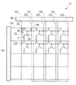
図1に示すように、有機エレクトロルミネッセンス表示装置(以下、適宜「有機EL表示装置」と称する)S1は、基板と、基板上に配線された複数の走査線131と、これら走査線131に対して交差する方向に延びるように配線された複数のデータ線132と、これらデータ線132に並列に延びるように配線された複数の共通給電線133とを有しており、走査線131及びデータ線132の各交点に対応して、画素(画素領域素)ARが設けられて構成されたものである。
【0024】
データ線132に対しては、シフトレジスタ、レベルシフタ、ビデオライン、D/Aコンバータ、デコーダ、ラッチ回路及びアナログスイッチのうち少なくとも1つを備えるデータ線駆動回路90が電気的に接続されている。
一方、走査線131に対しては、シフトレジスタ、レベルシフタ及びデコーダのうち少なくとも1つを備える走査線駆動回路80が電気的に接続されている。
【0025】
なお、本実施形態では、データ線駆動回路90及び走査線駆動回路80はともに基板上に配置されているが、データ線駆動回路90及び走査線駆動回路80のそれぞれを基板上に配置するか、または基板の外に配置するかについては、適宜選択できる。
【0026】
また、図1に示すように、画素領域ARの各々には、走査線131を介して走査信号がゲート電極に供給される第1の薄膜トランジスタ22と、この第1の薄膜トランジスタ22を介してデータ線132から供給される画像信号を保持する保持容量capと、保持容量capによって保持された画像信号がゲート電極に供給される第2の薄膜トランジスタ24と、この第2の薄膜トランジスタ24を介して共通給電線133に電気的に接続したときに共通給電線133から駆動電流が流れ込む画素電極23と、この画素電極(陽極)23と対向電極(陰極)222との間に挟み込まれた発光素子3とが設けられている。なお、発光素子3としては、EL(エレクトロルミネッセンス)素子の他に、LED(発光ダイオード)素子、LD(レーザーダイオード)素子などの発光素子が挙げられる。
【0027】
走査線131を介して供給される走査信号により第1の薄膜トランジスタ22がオンとなると、そのときのデータ線132を介して供給されるデータ信号に対応する電荷が保持容量capに保持され、該保持容量capの状態に応じて、第2の薄膜トランジスタ24の導通状態が決まる。そして、第2の薄膜トランジスタ24のチャネルを介して共通給電線133から画素電極23に電流が流れ、さらに発光層60を通じて対向電極222に電流が流れることにより、発光層60は、これを流れる電流量に応じて発光する。
【0028】
次に、図2を参照しながら、各画素ARの平面構造について説明する。図2は、対向電極や有機エレクトロルミネッセンス素子を取り除いた状態での図1の拡大平面図である。図2に示すように、平面視長方形状に設定された画素電極23は、その四辺を、データ線132、共通給電線133、走査線131及び図示しない他の画素電極用の走査線によって囲まれている。なお、画素電極の形状は長方形に限られず、円形、長円形等の形状でもよい。後述するインクジェット法のように液体材料を用いて発光層などEL素子を構成する材料層を形成する場合は、画素電極を特に角のない円形や長円形などの形状とすることにより均一な材料層が得られる。
【0029】
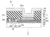
次に、有機EL表示装置の断面構造を図3を参照しながら説明する。図3は図2のA−A矢視断面図である。
ここで、図3に示す有機EL表示装置は、薄膜トランジスタ(TFT:Thin Film Transistor)が配置された基板2側から光を取り出す形態、いわゆるバックエミッション型である。したがって、本実施形態においては、基板2が、発光素子3からの光が取り出される最表面に位置する表面材料層となっている。なお、基板2の表面に他の材料層が積層された場合には、この他の材料層が表面材料層となる。
【0030】
図3に示すように、バックエミッション型の有機EL表示装置S1は、基板2と、インジウム錫酸化物(ITO:Indium Tin Oxide)等の透明電極材料からなる陽極(画素電極)23と、陽極23上に配置された発光素子3と、陽極23との間で発光素子3を挟み込むように配置されている陰極(対向電極)222と、基板2上に形成され、画素電極23に対する通電を制御する通電制御部としての薄膜トランジスタ(以下、「TFT」と称する)24とを有している。更に、陰極222の上層には封止層20が設けられている。陰極222は、アルミニウム(Al)やマグネシウム(Mg)、金(Au)、銀(Ag)、カルシウム(Ca)から選ばれる少なくとも1つの金属から構成されている。陰極222は上述した各材料の合金や積層したものをも含む。TFT24は、走査線駆動回路80及びデータ線駆動回路90からの作動指令信号に基づいて作動し、画素電極23への通電制御を行う。
【0031】
発光素子3は、陽極23から正孔を輸送可能な正孔輸送層70と、電気光学物質の1つである有機EL物質を含む発光層60と、発光層60の上面に設けられている電子輸送層50とから概略構成されている。そして、電子輸送層50の上面に陰極(対向電極)222が配置されている。
【0032】
TFT24は、SiO2を主体とする下地保護層281を介して基板2の表面に設けられている。このTFT24は、下地保護層281の上層に形成されたシリコン層241と、シリコン層241を覆うように下地保護層281の上層に設けられたゲート絶縁層282と、ゲート絶縁層282の上面のうちシリコン層241に対向する部分に設けられたゲート電極242と、ゲート電極242を覆うようにゲート絶縁層282の上層に設けられた第1層間絶縁層283と、ゲート絶縁層282及び第1層間絶縁層283にわたって開孔するコンタクトホールを介してシリコン層241と接続するソース電極243と、ゲート電極242を挟んでソース電極243と対向する位置に設けられ、ゲート絶縁層282及び第1層間絶縁層283にわたって開孔するコンタクトホールを介してシリコン層241と接続するドレイン電極244と、ソース電極243及びドレイン電極244を覆うように第1層間絶縁層283の上層に設けられた第2層間絶縁層284とを備えている。
【0033】
そして、第2層間絶縁層284の上面に画素電極23が配置され、画素電極23とドレイン電極244とは、第2層間絶縁層284に設けられたコンタクトホール23aを介して接続されている。また、第2層間絶縁層284の表面のうち発光素子(EL素子)3が設けられている以外の部分と陰極222との間には、合成樹脂などからなる第3絶縁層(バンク層)221が設けられている。
【0034】
なお、ドレイン電極244の上層に、TFTの保護層を設けても良い。この保護層の形成材料としては、珪素を含む絶縁層(特に窒化酸化珪素層又は窒化珪素層が好ましい)を用いることができる。この保護層は形成されたTFT24を金属イオンや水分から保護する役割を持つ。すなわち、保護層はこれらの金属イオンなど可動イオンをTFT24側に侵入させない保護層としても働く。
【0035】
また、保護層に放熱効果を持たせることで発光素子の熱劣化を防ぐことも有効である。ただし、発光素子として有機材料を用いる場合、酸素との結合により劣化するので、酸素を放出しやすい絶縁層は用いないことが好ましい。
【0036】
可動イオンの透過を妨げ、さらに放熱効果をもつ透光性材料としては、B(ホウ素)、C(炭素)、N(窒素)から選ばれた少なくとも一つの元素と、Al(アルミニウム)、Si(珪素)、P(リン)から選ばれた少なくとも一つの元素とを含む絶縁層が挙げられる。例えば、窒化アルミニウム(AlxNy)に代表されるアルミニウムの窒化物、炭化珪素(SixCy)に代表される珪素の炭化物、窒化珪素(SixNy)に代表される珪素の窒化物、窒化ホウ素(BxNy)に代表されるホウ素の窒化物、リン化ホウ素(BxPy)に代表されるホウ素のリン化物を用いることが可能である。また、酸化アルミニウム(AlxOy)に代表されるアルミニウムの酸化物は透光性に優れ熱伝導率が20Wm-1Kー 1であり、好ましい材料の一つと言える。これらの材料には上記効果だけでなく、水分の侵入を防ぐ効果もある。
【0037】
上記化合物に他の元素を組み合わせることもできる。例えば、酸化アルミニウムに窒素を添加して、AlNxOyで示される窒化酸化アルミニウムを用いることも可能である。この材料にも放熱効果だけでなく、水分や可動イオン等の侵入を防ぐ効果がある。
【0038】
また、Si、Al、N、O、Mを含む絶縁膜(但し、Mは希土類元素の少なくとも一種、好ましくはCe(セリウム),Yb(イッテルビウム),Sm(サマリウム),Er(エルビウム),Y(イットリウム)、La(ランタン)、Gd(ガドリニウム)、Dy(ジスプロシウム)、Nd(ネオジウム)から選ばれた少なくとも一つの元素)を用いることもできる。これらの材料にも放熱効果だけでなく、水分や可動イオンの侵入を防ぐ効果がある。
【0039】
また、少なくともダイヤモンド薄膜又はアモルファスカーボン膜(特にダイヤモンドに特性の近いもの、ダイヤモンドライクカーボン等と呼ばれる。)を含む炭素膜を用いることもできる。これらは非常に熱伝導率が高く、放熱層として極めて有効である。但し、膜厚が厚くなると褐色を帯びて透過率が低下するため、なるべく薄い膜厚(好ましくは5〜100nm)で用いることが好ましい。
【0040】
なお、保護層の目的はあくまで可動イオンや水分からTFTを保護することにあるので、その効果を損なうものでないことが好ましい。したがって、上記放熱効果をもつ材料からなる薄膜を単体で用いることもできるが、これらの薄膜と、可動イオンや水分の透過を妨げうる絶縁膜(代表的には窒化珪素膜(SixNy)や窒化酸化珪素膜(SiOxNy))とを積層することは有効である。
【0041】
シリコン層241のうち、ゲート絶縁層282を挟んでゲート電極242と重なる領域がチャネル領域とされている。また、シリコン層241のうち、チャネル領域のソース側にはソース領域が設けられている。一方、チャネル領域のドレイン側にはドレイン領域が設けられている。このうち、ソース領域が、ゲート絶縁層282と第1層間絶縁層283とにわたって開孔するコンタクトホールを介して、ソース電極243に接続されている。一方、ドレイン領域が、ゲート絶縁層282と第1層間絶縁層283とにわたって開孔するコンタクトホールを介して、ソース電極243と同一層からなるドレイン電極244に接続されている。画素電極23は、ドレイン電極244を介して、シリコン層241のドレイン領域に接続されている。
【0042】
本例では、発光層60からの発光光をTFT24が設けられている基板2側から取り出す構成(バックエミッション型)であるため、基板2の形成材料としては、光を透過可能な透明あるいは半透明材料、例えば、透明なガラス、石英、サファイア、あるいはポリエステル、ポリアクリレート、ポリカーボネート、ポリエーテルケトンなどの透明な合成樹脂などが用いられる。特に、基板の形成材料としては、安価なソーダガラスが好適に用いられる。ソーダガラスを用いた場合、これにシリカコートを施すのが、酸アルカリに弱いソーダガラスを保護する効果を有し、さらに基板の平坦性をよくする効果も有するため好ましい。
また、基板に色フィルター膜や発光性物質を含む色変換膜、あるいは誘電体反射膜を配置して、発光色を制御するようにしてもよい。
【0043】
一方、TFT24が設けられている基板2とは反対側から発光光を取り出す構成(トップエミッション型)である場合には、基板2は不透明であってもよく、その場合、アルミナ等のセラミック、ステンレス等の金属シートに表面酸化などの絶縁処理を施したもの、熱硬化性樹脂、熱可塑性樹脂などを用いることができる。
【0044】
下地保護層281を形成する際には、基板2に対し、TEOS(テトラエトキシシラン)や酸素ガスなどを原料としてプラズマCVD法によって製膜することにより、下地保護層281として厚さ約200〜500nmのシリコン酸化膜が形成される。
【0045】
シリコン層241を形成する際には、まず、基板2の温度を約350℃に設定して、下地保護膜281の表面にプラズマCVD法あるいはICVD法により厚さ約30〜70nmのアモルファスシリコン層を形成する。次いで、このアモルファスシリコン層に対してレーザアニール法、急速加熱法、または固相成長法などによって結晶化工程を行い、アモルファスシリコン層をポリシリコン層に結晶化する。レーザアニール法では、例えばエキシマレーザでビームの長寸が400mmのラインビームを用い、その出力強度は例えば200mJ/cm2 とする。ラインビームについては、その短寸方向におけるレーザ強度のピーク値の90%に相当する部分が各領域毎に重なるようにラインビームを走査する。次いで、ポリシリコン層をフォトリソグラフィ法によってパターンニングして、島状のシリコン層241とする。
【0046】
なお、シリコン層241は、図1に示した第2の薄膜トランジスタ24のチャネル領域及びソース・ドレイン領域となるものであるが、異なる断面位置においては第1の薄膜トランジスタ22のチャネル領域及びソース・ドレイン領域となる半導体膜も形成されている。つまり、二種類のトランジスタ22、24は同時に形成されるが、同じ手順で作られるため、以下の説明において、トランジスタに関しては、第2の薄膜トランジスタ24についてのみ説明し、第1の薄膜トランジスタ22についてはその説明を省略する。
【0047】
ゲート絶縁層282を形成する際には、シリコン層241の表面に対して、TEOSや酸素ガスなどを原料としてプラズマCVD法を用いて製膜することにより、厚さ約60〜150nmのシリコン酸化膜または窒化膜からなるゲート絶縁層282が形成される。
【0048】
ゲート電極242は、ゲート絶縁層282上にアルミニウム、タンタル、モリブデン、チタン、タングステンなどの金属を含む導電膜をスパッタ法により形成した後、これをパターニングすることにより形成される。
【0049】
シリコン層241にソース領域及びドレイン領域を形成するには、ゲート電極242を形成した後、このゲート電極242をパターニング用マスクとして用い、この状態でリンイオンを注入する。その結果、ゲート電極242に対してセルフアライン的に高濃度不純物が導入されて、シリコン層241中にソース領域及びドレイン領域が形成される。なお、不純物が導入されなかった部分がチャネル領域となる。
【0050】
第1層間絶縁層283は、基板2より屈折率が低い低屈折率材料からなり、ゲート絶縁層282の上層に形成される。
第1層間絶縁層283の形成材料としては、シリコン酸化膜、窒化膜、あるいは多孔性を有するシリコン酸化膜(SiO2膜)などが挙げられる。多孔性を有するSiO2膜からなるゲート絶縁層282は、反応ガスとしてSi2H6とO3とを用いて、CVD法(化学的気相成長法)により形成される。これらの反応ガスを用いると、気相中に粒子の大きいSiO2が形成され、ゲート絶縁層282の上に堆積する。そのため、第1層間絶縁層283は、層中に多くの空隙を有し、多孔質体となる。そして、第1層間絶縁層283は多孔質体となることによって低屈折率材料となり、光の取り出し効率が向上できる。
【0051】
多孔質体からなる低屈折率層は、密度が0.4g/cm3以下であることが好ましい。
【0052】
低屈折率層としての第1層間絶縁層283の屈折率は1.5以下、好ましくは1.2以下に設定される。
【0053】
なお、第1層間絶縁層283の表面にH(水素)プラズマ処理をしてもよい。これにより、空隙の表面のSi−O結合中のダングリングボンドがSi−H結合に置き換えられ、膜の耐吸湿性が良くなる。そして、このプラズマ処理された第1絶縁層283の表面に別のSiO2層を設けてもよい。
また、第1層間絶縁層283をCVD法で形成する際の反応ガスは、Si2H6+O3の他に、Si2H6+O2、Si3H8+O3、Si3H8+O2としてもよい。更に、上記の反応ガスに加えて、B(ホウ素)含有の反応ガス、F(フッ素)含有の反応ガスを用いてもよい。
【0054】
第1層間絶縁層283を多孔質体として形成する際、多孔性を有するSiO2膜と、通常の減圧化学的気相成長法により形成されたSiO2膜とを積層することにより、膜質の安定した多孔質体としての第1層間絶縁層283を形成することもできる。そして、これらの膜を積層するには、減圧下におけるSiH4とO2の雰囲気中において、プラズマを断続的、又は周期的に発生させることによって可能となる。具体的には、第1層間絶縁層283は、基板2を所定のチャンバ内に収容し、例えば400℃に保持しながら、反応ガスとしてSiH4とO2を用い、RF電圧(高周波電圧)をチャンバに印加することにより形成される。成膜中においては、SiH4流量、O2流量が一定であるのに対し、RF電圧は10秒の周期でチャンバに印加される。これにともない、プラズマが10秒の周期で発生、消滅する。このように、時間変化するプラズマを用いることにより、1つのチャンバー内で、減圧CVDを用いるプロセスと、減圧下におけるプラズマCVDを用いるプロセスとを繰り返し行うことができる。そして、減圧CVDと減圧下におけるプラズマCVDとを繰り返し行うことにより、膜中に多数の空隙を有するSiO2膜が形成される。すなわち、第1層間絶縁層283は多孔性を有することになる。
【0055】
第1層間絶縁層283は、エアロゲルによって構成することもできる。エアロゲルとは、金属アルコキシドのゾルゲル反応により形成される湿潤ゲルを超臨界乾燥することによって得られる均一な超微細構造を持った光透過性の多孔質体である。エアロゲルにはシリカエアロゲルやアルミナを基調としたエアロゲルがある。このうち、シリカエアロゲルは、体積の90%以上を空隙が占め、残りが樹枝状に凝集した数10nmの微細なSiO2粒子で構成された材料であり、粒子径が光の波長よりも小さいため、光透過性を有し、その屈折率は1.2以下である。また、空隙率を変化させることによって屈折率を調整できる。ここで、基板2の材料であるガラスの屈折率は1.54、石英の屈折率は1.45である。
【0056】
シリカエアロゲルは、ゾル−ゲル法により湿潤ゲルを作製する工程、湿潤ゲルを熟成させる工程、及び超臨界乾燥法により湿潤ゲルを乾燥してエアロゲルを得る超臨界乾燥工程を経て製造される。超臨界乾燥法は、固相と液相とからなるゼリー状のゲル物質中の液体を超臨界流体と置換、除去することにより、ゲルを収縮させることなくゲル物質を乾燥するのに適した方法であって、高い空隙率を有するエアロゲルが得られる。
【0057】
例えば第1層間絶縁層283をシリカエアロゲルによって形成する際には、ゲート絶縁層282の上にエアロゲルの原料である湿潤ゲルをスピンコート法等を用いてコーティングし、超臨界乾燥することにより形成される。超臨界流体を用いた超臨界乾燥法によって、湿潤ゲル中の溶媒を超臨界流体で置換することにより、湿潤ゲル中の溶媒が除去される。なお、超臨界流体としては、二酸化炭素(CO2)、若しくは、メタノールやエタノールのようなアルコール、NH3、H2O、N2O、メタン、エタン、エチレン、プロパン、ペンタン、イソプロパノール、イソブタノール、シクロトリフルオロメタン、モノフルオロメタン、シクロヘキサノールなどを用いることができる。
【0058】
低屈折率層(各絶縁層)をシリカエアロゲルによって形成する際、基材上にスピンコートなどによって湿潤ゲルを塗布した後、超臨界乾燥するが、湿潤ゲルに合成樹脂(有機物)を混合しておいてもよい。この場合の合成樹脂は、その熱変性温度が超臨界流体の臨界温度よりも高く光を透過可能な合成樹脂である。超臨界流体として例えばアルコールを用いた場合、その熱変性温度がアルコールの臨界温度よりも高く光を透過可能な合成樹脂としては、ヒドロキシルプロピルセルロース(HPC),ポリビニルブチラール(PVB),エチルセルロース(EC)等が挙げられる(なお、PVB及びECはアルコールに可溶で水には不溶)。溶媒としてエーテルを用いる場合には樹脂として塩素系ポリエチレン等を選択し、またCO2を溶媒として用いる場合にはHPC等を選択することが望ましい。
【0059】
低屈折率層としては、シリカエアロゲルの他にアルミナを基調としたエアロゲルでもよく、基板2より低屈折率で光を透過可能な多孔質体であればよい。そして、多孔質体(エアロゲル)は密度が0.4g/cm3以下であることが好ましい。
【0060】
低屈折率層としては多孔質体でなくてもよく、エポキシ系接着剤(屈折率:1.42)やアクリル系接着剤(屈折率:1.43)など、光を透過可能で基板2より低屈折率な高分子材料からなる接着剤でもよい。これらの接着剤を単独で使用した場合であっても、基板2を構成するガラスや石英よりも屈折率が低いため、光の取り出し効率を向上できる。
【0061】
更に、低屈折率層としては、多孔質シリカでもよいし、フッ化マグネシウム(屈折率:1.38)あるいはこれを含む材料でもよい。フッ化マグネシウムによる低屈折率層はスパッタリングによって形成可能である。あるいは、フッ化マグネシウムの微粒子を分散したゲルでもよい。あるいは、フッ素系ポリマー又はこれを含む材料、例えば、パーフルオロアルキル−ポリエーテル、パーフルオロアルキルアミン、またはパーフルオロアルキル−ポリエーテル−パーフルオロアルキルアミン混合フィルムでもよい。
【0062】
更には、低屈折率層として、所定のポリマーバインダーに、可溶性もしくは分散性である低屈折率のフルオロカーボン化合物を混在したものでもよい。
ポリマーバインダーとしては、ポリビニルアルコール、ポリアクリル酸、ポリビニルピロリドン、ポリビニルスルホン酸ナトリウム塩、ポリビニルメチルエーテル、ポリエチレングリコール、ポリα−トリフルオロメチルアクリル酸、ポリビニルメチルエーテル−コ−無水マレイン酸、ポリエチレングリコール−コ−プロピレングリコール、ポリメタアクリル酸などが挙げられる。
また、フルオロカーボン化合物としては、パーフルオロオクタン酸−アンモニウム塩、パーフルオロオクタン酸−テトラメチルアンモニウム塩、C−7とC−10のパーフルオロアルキルスルホン酸アンモニウム塩、C−7とC−10のパーフルオロアルキルスルホン酸テトラメチルアンモニウム塩、フッ素化アルキル第4級アンモニウムアイオダイド、パーフルオロアジピン酸、およびパーフルオロアジピン酸の第4級アンモニウム塩などが挙げられる。
【0063】
更に、低屈折率層として空隙を導入する方法が有効であるため、上記エアロゲルの他に、微粒子を用いて微粒子間または微粒子内のミクロボイドとして空隙を形成してもよい。微粒子としては、無機微粒子あるいは有機微粒子を低屈折率層に用いることができる。
無機微粒子は、非晶質であることが好ましい。無機微粒子は、金属の酸化物、窒化物、硫化物またはハロゲン化物からなることが好ましく、金属酸化物または金属ハロゲン化物からなることがさらに好ましく、金属酸化物または金属フッ化物からなることが最も好ましい。金属原子としては、Na、K、Mg、Ca、Ba、Al、Zn、Fe、Cu、Ti、Sn、In、W、Y、Sb、Mn、Ga、V、Nb、Ta、Ag、Si、B、Bi、Mo、Ce、Cd、Be、PbおよびNiが好ましく、Mg、Ca、BおよびSiがさらに好ましい。二種類の金属を含む無機化合物を用いてもよい。特に好ましい無機化合物は、二酸化ケイ素、すなわちシリカである。
【0064】
無機微粒子内ミクロボイドは、例えば、粒子を形成するシリカの分子を架橋させることにより形成することができる。シリカの分子を架橋させると体積が縮小し、粒子が多孔質になる。ミクロボイドを有する(多孔質)無機微粒子は、ゾル−ゲル法(特開昭53−112732号、特公昭57−9051号の各公報記載)または析出法(APPLIED OPTICS、27、3356頁(1988)記載)により、分散物として直接合成することができる。また、乾燥・沈澱法で得られた粉体を、機械的に粉砕して分散物を得ることもできる。市販の多孔質無機微粒子(例えば、二酸化ケイ素ゾル)を用いてもよい。ミクロボイドを有する無機微粒子は、低屈折率層の形成のため、適当な媒体に分散した状態で使用することが好ましい。分散媒としては、水、アルコール(例、メタノール、エタノール、イソプロピルアルコール)およびケトン(例、メチルエチルケトン、メチルイソブチルケトン)が好ましい。
【0065】
有機微粒子も、非晶質であることが好ましい。有機微粒子は、モノマーの重合反応(例えば乳化重合法)により合成されるポリマー微粒子であることが好ましい。有機微粒子のポリマーはフッ素原子を含むことが好ましい。含フッ素ポリマーを合成するために用いるフッ素原子を含むモノマーの例には、フルオロオレフィン類(例、フルオロエチレン、ビニリデンフルオライド、テトラフルオロエチレン、ヘキサフルオロプロピレン、パーフルオロ−2,2−ジメチル−1,3−ジオキソール)、アクリル酸またはメタクリル酸のフッ素化アルキルエステル類およびフッ素化ビニルエーテル類が含まれる。フッ素原子を含むモノマーとフッ素原子を含まないモノマーとのコポリマーを用いてもよい。フッ素原子を含まないモノマーの例には、オレフィン類(例、エチレン、プロピレン、イソプレン、塩化ビニル、塩化ビニリデン)、アクリル酸エステル類(例、アクリル酸メチル、アクリル酸エチル、アクリル酸2−エチルヘキシル)、メタクリル酸エステル類(例、メタクリル酸メチル、メタクリル酸エチル、メタクリル酸ブチル)、スチレン類(例、スチレン、ビニルトルエン、α−メチルスチレン)、ビニルエーテル類(例、メチルビニルエーテル)、ビニルエステル類(例、酢酸ビニル、プロピオン酸ビニル)、アクリルアミド類(例、N−tert−ブチルアクリルアミド、N−シクロヘキシルアクリルアミド)、メタクリルアミド類およびアクリルニトリル類が含まれる。
【0066】
有機微粒子内ミクロボイドは、例えば、粒子を形成するポリマーを架橋させることにより形成することができる。ポリマーを架橋させると体積が縮小し、粒子が多孔質になる。粒子を形成するポリマーを架橋させるためには、ポリマーを合成するためのモノマーの20モル%以上を多官能モノマーとすることが好ましい。多官能モノマーの割合は、30乃至80モル%であることがさらに好ましく、35乃至50モル%であることが最も好ましい。多官能モノマーの例には、ジエン類(例、ブタジエン、ペンタジエン)、多価アルコールとアクリル酸とのエステル(例、エチレングリコールジアクリレート、1,4−シクロヘキサンジアクリレート、ジペンタエリスリトールヘキサアクリレート)、多価アルコールとメタクリル酸とのエステル(例、エチレングリコールジメタクリレート、1,2,4−シクロヘキサンテトラメタクリレート、ペンタエリスリトールテトラメタクリレート)、ジビニル化合物(例、ジビニルシクロヘキサン、1,4−ジビニルベンゼン)、ジビニルスルホン、ビスアクリルアミド類(例、メチレンビスアクリルアミド)およびビスメタクリルアミド類が含まれる。粒子間のミクロボイドは、微粒子を少なくとも2個以上積み重ねることにより形成することができる。
【0067】
低屈折率層を、微細空孔と微粒子状無機物とを有する材料によって構成してもよい。この場合、低屈折率層はコーティングにより形成され、微細空孔は層の塗布後に活性化ガス処理を行ない、ガスが層から離脱することによって形成される。あるいは、2種類以上の超微粒子(例えば、MgF2とSiO2 )を混在させて、膜厚方向にその混合比を変化させることによって低屈折率層を形成してもよい。混合比を変化させることにより屈折率が変化する。超微粒子は、エチルシリケートの熱分解で生じたSiO2により接着している。エチルシリケートの熱分解では、エチル部分の燃焼によって、二酸化炭素と水蒸気も発生する。二酸化炭素と水蒸気が層から離脱することにより、超微粒子の間に間隙が生じている。あるいは、多孔質シリカよりなる無機微粉末とバインダーとを含有して低屈折率層を形成してもよいし、含フッ素ポリマーからなる微粒子を2個以上積み重ねることにより、微粒子間に空隙を形成した低屈折率層を形成してもよい。
【0068】
分岐構造レベルで空隙率を向上させることもできる。例えばデンドリマーなどの分岐構造を有するポリマーを用いても低屈折率が得られる。
【0069】
そして、上記の材料を用いて、低屈折率層は、屈折率が1.5以下、好ましくは1.2以下に設定されていることが望ましい。基板2として屈折率が1.45の石英や、屈折率が約1.54のガラスなどを用いた際、基板2の屈折率より低い屈折率となる。
【0070】
ソース電極243及びドレイン電極244を形成するには、まず、第1層間絶縁層283にフォトリソグラフィ法を用いてパターニングすることにより、ソース電極及びドレイン電極に対応するコンタクトホールを形成する。次に、第1層間絶縁層283を覆うように、アルミニウムやクロム、タンタル等の金属からなる導電層を形成した後、この導電層のうち、ソース電極及びドレイン電極が形成されるべき領域を覆うようにパターニング用マスクを設けるとともに、導電層をパターニングすることにより、ソース電極243及びドレイン電極244が形成される。
【0071】
第2層間絶縁層284は、第1層間絶縁層283同様、低屈折率材料によって構成され、第1層間絶縁層283の形成方法と同様の手順で第1層間絶縁層283の上層に形成される。ここで、第2層間絶縁層284を形成したら、第2層間絶縁層284のうちドレイン電極244に対応する部分にコンタクトホール23aを形成する。
【0072】
発光素子3に接続する陽極23は、ITOやフッ素をドープしてなるSnO2、更にZnOやポリアミン等の透明電極材料からなり、コンタクトホール23aを介してTFT24のドレイン電極244に接続されている。陽極23を形成するには、前記透明電極材料からなる膜を第2層間絶縁層284上面に形成し、この膜をパターニングすることにより形成される。
【0073】
第3絶縁層(バンク層)221はアクリル樹脂、ポリイミド樹脂などの合成樹脂によって構成されている。第3絶縁層221は、陽極23が形成された後に形成される。具体的な第3絶縁層221の形成方法としては、例えば、アクリル樹脂、ポリイミド樹脂などのレジストを溶媒に融かしたものを、スピンコート、ディップコート等により塗布して絶縁層を形成する。なお、絶縁層の構成材料は、後述するインクの溶媒に溶解せず、しかもエッチング等によってパターニングしやすいものであればどのようなものでもよい。更に、絶縁層をフォトリソグラフィ技術等により同時にエッチングして、開口部221aを形成することにより、開口部221aを備えた第3絶縁層221が形成される。
【0074】
ここで、第3絶縁層221の表面には、親液性(親インク性)を示す領域と、撥液性(撥インク性)を示す領域とが形成される。本実施形態においてはプラズマ処理工程により、各領域を形成するものとしている。具体的にプラズマ処理工程は、予備加熱工程と、開口部221aの壁面並びに画素電極23の電極面を親インク性にする親インク化工程と、第3絶縁層221の上面を撥インク性にする撥インク化工程と、冷却工程とを有している。
すなわち、基材(第3絶縁層等を含む基板2)を所定温度(例えば70〜80土程度)に加熱し、次いで親インク化工程として大気雰囲気中で酸素を反応ガスとするプラズマ処理(O2プラスマ処理)を行う。続いて、撥インク化工程として大気雰囲気中で4フッ化メタンを反応ガスとするプラスマ処理(CF4プラスマ処理)を行い、プラズマ処理のために加熱された基材を室温まで冷却することで、親インク性及び撥インク性が所定箇所に付与されることとなる。なお、画素電極23の電極面についても、このCF4プラスマ処理の影響を多少受けるが、画素電極23の材料であるITO等はフッ素に対する親和性に乏しいため、親インク化工程で付与された水酸基がフッ素基で置換されることがなく、親インク性が保たれる。
【0075】
なお、第1層間絶縁層283、第2層間絶縁層284のそれぞれを低屈折率層としているが、これら2つの層を低屈折率層とする必要はなく、少なくともいずれか一方の層だけ低屈折率層としてもよい。
【0076】
一方、第1層間絶縁層283及び第2層間絶縁層284に加えて、ゲート絶縁層282も低屈折率材料により形成してもよい。こうすることにより光の取り出し効率が向上するが、TFTなどトランジスタの性能を向上させるためにはゲート絶縁層を高誘電率材料により形成することが好ましい場合がある。
【0077】
また、低屈折率材料からなる層は発光層60からの光が通過する部分に設けられていればよいので、絶縁層以外の層を低屈折率層としてもよい。更には、有機バンク層221を低屈折率層としてもよい。
【0078】
正孔輸送層70は陽極23の上面に形成されている。ここで、正孔輸送層70の形成材料としては、特に限定されることなく公知のものが使用可能であり、例えばピラゾリン誘導体、アリールアミン誘導体、スチルベン誘導体、トリフェニルジアミン誘導体等が挙げられる。具体的には、特開昭63−70257号、同63−175860号公報、特開平2−135359号、同2−135361号、同2−209988号、同3−37992号、同3−152184号公報に記載されているもの等が例示されるが、トリフェニルジアミン誘導体が好ましく、中でも4,4’−ビス(N(3−メチルフェニル)−N−フェニルアミノ)ビフェニルが好適とされる。
【0079】
なお、正孔輸送層に代えて正孔注入層を形成するようにしてもよく、さらに正孔注入層と正孔輸送層を両方形成するようにしてもよい。その場合、正孔注入層の形成材料としては、例えば銅フタロシアニン(CuPc)や、ポリテトラヒドロチオフェニルフェニレンであるポリフェニレンビニレン、1,1−ビス−(4−N,N−ジトリルアミノフェニル)シクロヘキサン、トリス(8−ヒドロキシキノリノール)アルミニウム等が挙げられるが、特に銅フタロシアニン(CuPc)を用いるのが好ましい。
【0080】
正孔注入/輸送層70を形成する際には、インクジェット法が用いられる。すなわち、上述した正孔注入/輸送層材料を含む組成物インクを陽極23の電極面上に吐出した後に、乾燥処理及び熱処理を行うことにより、電極23上に正孔注入/輸送層70が形成される。なお、この正孔注入/輸送層形成工程以降は、正孔注入/輸送層70及び発光層(有機EL層)60の酸化を防止すべく、窒素雰囲気、アルゴン雰囲気等の不活性ガス雰囲気で行うことが好ましい。例えば、インクジェットヘッド(不図示)に正孔注入/輸送層材料を含む組成物インクを充填し、インクジェットヘッドの吐出ノズルを陽極23の電極面に対向させ、インクジェットヘッドと基材(基板2)とを相対移動させながら、吐出ノズルから1滴当たりの液量が制御されたインキ滴を電極面に吐出する。次に、吐出後のインク滴を乾燥処理して組成物インクに含まれる極性溶媒を蒸発させることにより、正孔注入/輸送層70が形成される。
【0081】
なお、組成物インクとしては、例えば、ポリエチレンジオキシチオフェン等のポリチオフェン誘導体と、ポリスチレンスルホン酸等との混合物を、イソプロピルアルコール等の極性溶媒に溶解させたものを用いることができる。ここで、吐出されたインク滴は、親インク処理された陽極23の電極面上に広がり、開口部221aの底部近傍に満たされる。その一方で、撥インク処理された第3絶縁層221の上面にはインク滴がはじかれて付着しない。したがって、インク滴が所定の吐出位置からはずれて第3絶縁層221の上面に吐出されたとしても、該上面がインク滴で濡れることがなく、はじかれたインク滴が第3絶縁層221の開口部221a内に転がり込むものとされている。
【0082】
発光層60は、正孔注入/輸送層70上面に形成される。発光層60の形成材料としては、特に限定されることなく、低分子の有機発光色素や高分子発光体、すなわち各種の蛍光物質や燐光物質からなる発光物質が使用可能である。発光物質となる共役系高分子の中ではアリーレンビニレン構造を含むものが特に好ましい。低分子蛍光体では、例えばナフタレン誘導体、アントラセン誘導体、ペリレン誘導体、ポリメチン系、キサテン系、クマリン系、シアニン系などの色素類、8−ヒドロキノリンおよびその誘導体の金属錯体、芳香族アミン、テトラフェニルシクロペンタジエン誘導体等、または特開昭57−51781、同59−194393号公報等に記載されている公知のものが使用可能である。
【0083】
発光層60の形成材料として高分子蛍光体を用いる場合には、側鎖に蛍光基を有する高分子を用いることができるが、好ましくは共役系構造を主鎖に含むもので、特に、ポリチオフェン、ポリ−p−フェニレン、ポリアリーレンビニレン、ポリフルオレンおよびその誘導体が好ましい。中でもポリアリーレンビニレンおよびその誘導体が好ましい。該ポリアリーレンビニレンおよびその誘導体は、下記化学式(1)で示される繰り返し単位を全繰り返し単位の50モル%以上含む重合体である。繰り返し単位の構造にもよるが、化学式(1)で示される繰り返し単位が全繰り返し単位の70%以上であることがさらに好ましい。
−Ar−CR=CR’− (1)
〔ここで、Arは、共役結合に関与する炭素原子数が4個以上20個以下からなるアリーレン基または複素環化合物基、R、R’はそれぞれ独立に水素、炭素数1〜20のアルキル基、炭素数6〜20のアリール基、炭素数4〜20の複素環化合物、シアノ基からなる群から選ばれた基を示す。〕
【0084】
該高分子蛍光体は、化学式(1)で示される繰り返し単位以外の繰り返し単位として、芳香族化合物基またはその誘導体、複素環化合物基またはその誘導体、およびそれらを組み合わせて得られる基などを含んでいてもよい。また、化学式(1)で示される繰り返し単位や他の繰り返し単位が、エーテル基、エステル基、アミド基、イミド基などを有する非共役の単位で連結されていてもよいし、繰り返し単位にそれらの非共役部分が含まれていてもよい。
【0085】
前記高分子蛍光体において化学式(1)のArとしては、共役結合に関与する炭素原子数が4個以上20個以下からなるアリーレン基または複素環化合物基であり、下記の化学式(2)で示す芳香族化合物基またはその誘導体基、複素環化合物基またはその誘導体基、およびそれらを組み合わせて得られる基などが例示される。
【0086】
【化1】
【0087】
これらのなかでフェニレン基、置換フェニレン基、ビフェニレン基、置換ビフェニレン基、ナフタレンジイル基、置換ナフタレンジイル基、アントラセン−9,10−ジイル基、置換アントラセン−9,10−ジイル基、ピリジン−2,5−ジイル基、置換ピリジン−2,5−ジイル基、チエニレン基および置換チエニレン基が好ましい。さらに好ましくは、フェニレン基、ビフェニレン基、ナフタレンジイル基、ピリジン−2,5−ジイル基、チエニレン基である。
【0088】
化学式(1)のR、R’が水素またはシアノ基以外の置換基である場合について述べると、炭素数1〜20のアルキル基としては、メチル基、エチル基、プロピル基、ブチル基、ペンチル基、ヘキシル基、ヘプチル基、オクチル基、デシル基、ラウリル基などが挙げられ、メチル基、エチル基、ペンチル基、ヘキシル基、ヘプチル基、オクチル基が好ましい。アリール基としては、フェニル基、4−C1〜C12アルコキシフェニル基(C1〜C12は炭素数1〜12であることを示す。以下も同様である。)、4−C1〜C12アルキルフェニル基、1−ナフチル基、2−ナフチル基などが例示される。
【0089】
溶媒可溶性の観点からは化学式(1)のArが、1つ以上の炭素数4〜20のアルキル基、アルコキシ基およびアルキルチオ基、炭素数6〜18のアリール基およびアリールオキシ基ならびに炭素数4〜14の複素環化合物基から選ばれた基を有していることが好ましい。
【0090】
これらの置換基としては以下のものが例示される。炭素数4〜20のアルキル基としては、ブチル基、ペンチル基、ヘキシル基、ヘプチル基、オクチル基、デシル基、ラウリル基などが挙げられ、ペンチル基、ヘキシル基、ヘプチル基、オクチル基が好ましい。また、炭素数4〜20のアルコキシ基としては、ブトキシ基、ペンチルオキシ基、ヘキシルオキシ基、ヘプチルオキシ基、オクチルオキシ基、デシルオキシ基、ラウリルオキシ基などが挙げられ、ペンチルオキシ基、ヘキシルオキシ基、ヘプチルオキシ基、オクチルオキシ基が好ましい。炭素数4〜20のアルキルチオ基としては、ブチルチオ基、ペンチルチオ基、ヘキシルチオ基、ヘプチルチオ基、オクチルチオ基、デシルオキシ基、ラウリルチオ基などが挙げられ、ペンチルチオ基、ヘキシルチオ基、ヘプチルチオ基、オクチルチオ基が好ましい。アリール基としては、フェニル基、4−C1〜C12アルコキシフェニル基、4−C1〜C12アルキルフェニル基、1−ナフチル基、2−ナフチル基などが例示される。アリールオキシ基としては、フェノキシ基が例示される。複素環化合物基としては2−チエニル基、2−ピロリル基、2−フリル基、2−、3−または4−ピリジル基などが例示される。これら置換基の数は、該高分子蛍光体の分子量と繰り返し単位の構成によっても異なるが、溶解性の高い高分子蛍光体を得る観点から、これらの置換基が分子量600当たり1つ以上であることがより好ましい。
【0091】
なお、前記高分子蛍光体は、ランダム、ブロックまたはグラフト共重合体であってもよいし、それらの中間的な構造を有する高分子、例えばブロック性を帯びたランダム共重合体であってもよい。蛍光の量子収率の高い高分子蛍光体を得る観点からは完全なランダム共重合体よりブロック性を帯びたランダム共重合体やブロックまたはグラフト共重合体が好ましい。また、ここで形成する有機エレクトロルミネッセンス素子は、薄膜からの蛍光を利用することから、該高分子蛍光体は固体状態で蛍光を有するものが用いられる。
【0092】
該高分子蛍光体に対して溶媒を使用する場合に、好適なものとしては、クロロホルム、塩化メチレン、ジクロロエタン、テトラヒドロフラン、トルエン、キシレンなどが例示される。高分子蛍光体の構造や分子量にもよるが、通常はこれらの溶媒に0.1wt%以上溶解させることができる。
また、前記高分子蛍光体としては、分子量がポリスチレン換算で103 〜107 であることが好ましく、それらの重合度は繰り返し構造やその割合によっても変わる。成膜性の点から一般には繰り返し構造の合計数で好ましくは4〜10000、さらに好ましくは5〜3000、特に好ましくは10〜2000である。
【0093】
このような高分子蛍光体の合成法としては、特に限定されないものの、例えばアリーレン基にアルデヒド基が2つ結合したジアルデヒド化合物と、アリーレン基にハロゲン化メチル基が2つ結合した化合物とトリフェニルホスフィンとから得られるジホスホニウム塩からのWittig反応が例示される。また、他の合成法としては、アリーレン基にハロゲン化メチル基が2つ結合した化合物からの脱ハロゲン化水素法が例示される。さらに、アリーレン基にハロゲン化メチル基が2つ結合した化合物のスルホニウム塩をアルカリで重合して得られる中間体から熱処理により該高分子蛍光体を得るスルホニウム塩分解法が例示される。いずれの合成法においても、モノマーとして、アリーレン基以外の骨格を有する化合物を加え、その存在割合を変えることにより、生成する高分子蛍光体に含まれる繰り返し単位の構造を変えることができるので、化学式(1)で示される繰り返し単位が50モル%以上となるように加減して仕込み、共重合してもよい。これらのうち、Wittig反応による方法が、反応の制御や収率の点で好ましい。
【0094】
さらに具体的に、前記高分子蛍光体の1つの例であるアリーレンビニレン系共重合体の合成法を説明する。例えば、Wittig反応により高分子蛍光体を得る場合には、例えばまず、ビス(ハロゲン化メチル)化合物、より具体的には、例えば2,5−ジオクチルオキシ−p−キシリレンジブロミドをN,N−ジメチルホルムアミド溶媒中、トリフェニルホスフィンと反応させてホスホニウム塩を合成し、これとジアルデヒド化合物、より具体的には、例えば、テレフタルアルデヒドとを、例えばエチルアルコール中、リチウムエトキシドを用いて縮合させるWittig反応により、フェニレンビニレン基と2,5−ジオクチルオキシ−p−フェニレンビニレン基を含む高分子蛍光体が得られる。このとき、共重合体を得るために2種類以上のジホスホニウム塩および/または2種類以上のジアルデヒド化合物を反応させてもよい。
これらの高分子蛍光体を発光層の形成材料として用いる場合、その純度が発光特性に影響を与えるため、合成後、再沈精製、クロマトグラフによる分別等の純化処理をすることが望ましい。
【0095】
また、前記の高分子蛍光体からなる発光層の形成材料としては、フルカラー表示をなすため、赤、緑、青の三色の発光層形成材料が用いられ、それぞれが所定のパターニング装置(インクジェット装置)によって予め設定された位置の画素ARに射出され、パターニングされる。
なお、前記の発光物質としては、ホスト材料にゲスト材料を添加した形態のものを用いることもできる。
【0096】
このような発光材料としては、ホスト材料として例えば高分子有機化合物や低分子材料が、またゲスト材料として得られる発光層の発光特性を変化させるための蛍光色素、あるいは燐光物質を含んでなるものが好適に用いられる。
高分子有機化合物としては、溶解性の低い材料の場合、例えば前駆体が塗布された後、以下の化学式(3)に示すように加熱硬化されることによって共役系高分子有機エレクトロルミネッセンス層となる発光層を生成し得るものがある。例えば、前駆体のスルホニウム塩の場合、加熱処理されることによりスルホニウム基が脱離し、共役系高分子有機化合物となるもの等がある。
また、溶解性の高い材料では、材料をそのまま塗布した後、溶媒を除去して発光層にし得るものもある。
【0097】
【化2】
前記の高分子有機化合物は固体で強い蛍光を持ち、均質な固体超薄膜を形成することができる。しかも、形成能に富みITO電極との密着性も高く、さらに、固化した後は強固な共役系高分子膜を形成する。
【0099】
このような高分子有機化合物としては、例えばポリアリーレンビニレンが好ましい。ポリアリーレンビニレンは水系溶媒あるいは有機溶媒に可溶で第2の基体11に塗布する際の塗布液への調製が容易であり、さらに一定条件下でポリマー化することができるため、光学的にも高品質の薄膜を得ることができる。
このようなポリアリーレンビニレンとしては、PPV(ポリ(パラ−フェニレンビニレン))、MO−PPV(ポリ(2,5−ジメトキシ−1,4−フェニレンビニレン))、CN−PPV(ポリ(2,5−ビスヘキシルオキシ−1,4−フェニレン−(1−シアノビニレン)))、MEH−PPV(ポリ[2−メトキシ−5−(2’−エチルヘキシルオキシ)]−パラ−フェニレンビニレン)、等のPPV誘導体、PTV(ポリ(2,5−チエニレンビニレン))等のポリ(アルキルチオフェン)、PFV(ポリ(2,5−フリレンビニレン))、ポリ(パラフェニレン)、ポリアルキルフルオレン等が挙げられるが、なかでも化学式(4)に示すようなPPVまたはPPV誘導体の前駆体からなるものや、化学式(5)に示すようなポリアルキルフルオレン(具体的には化学式(6)に示すようなポリアルキルフルオレン系共重合体)が特に好ましい。
PPV等は強い蛍光を持ち、二重結合を形成するπ電子がポリマー鎖上で非極在化している導電性高分子でもあるため、高性能の有機エレクトロルミネッセンス素子を得ることができる。
【0100】
【化3】
【化4】
【化5】
なお、前記PPV薄膜の他に発光層を形成し得る高分子有機化合物や低分子材料、すなわち本例においてホスト材料として用いられるものは、例えばアルミキノリノール錯体(Alq3)やジスチリルビフェニル、さらに化学式(7)に示すBeBq2やZn(OXZ)2 、そしてTPD、ALO、DPVBi等の従来より一般的に用いられているものに加え、ピラゾリンダイマー、キノリジンカルボン酸、ベンゾピリリウムパークロレート、ベンゾピラノキノリジン、ルブレン、フェナントロリンユウロピウム錯体等が挙げられ、これらの1種または2種以上を含む有機エレクトロルミネッセンス素子用組成物を用いることができる。
【0104】
【化6】
一方、このようなホスト材料に添加されるゲスト材料としては、前記したように蛍光色素や燐光物質が挙げられる。特に蛍光色素は、発光層の発光特性を変化させることができ、例えば、発光層の発光効率の向上、または光吸収極大波長(発光色)を変えるための手段としても有効である。すなわち、蛍光色素は単に発光層材料としてではなく、発光機能そのものを担う色素材料として利用することができる。例えば、共役系高分子有機化合物分子上のキャリア再結合で生成したエキシトンのエネルギーを蛍光色素分子上に移すことができる。この場合、発光は蛍光量子効率が高い蛍光色素分子からのみ起こるため、発光層の電流量子効率も増加する。したがって、発光層の形成材料中に蛍光色素を加えることにより、同時に発光層の発光スペクトルも蛍光分子のものとなるので、発光色を変えるための手段としても有効となる。
【0106】
なお、ここでいう電流量子効率とは、発光機能に基づいて発光性能を考察するための尺度であって、下記式により定義される。
ηE =放出されるフォトンのエネルギー/入力電気エネルギー
そして、蛍光色素のドープによる光吸収極大波長の変換によって、例えば赤、青、緑の3原色を発光させることができ、その結果フルカラー表示体を得ることが可能となる。
さらに蛍光色素をドーピングすることにより、エレクトロルミネッセンス素子の発光効率を大幅に向上させることができる。
【0107】
蛍光色素としては、赤色の発色光を発光する発光層を形成する場合、レーザー色素のDCM−1、あるいはローダミンまたはローダミン誘導体、ペニレン等を用いるのが好ましい。これらの蛍光色素をPPVなどホスト材料にドープすることにより、発光層を形成することができるが、これらの蛍光色素は水溶性のものが多いので、水溶性を有するPPV前駆体であるスルホニウム塩にドープし、その後、加熱処理すれば、より均一な発光層の形成が可能になる。このような蛍光色素として具体的には、ローダミンB、ローダミンBベース、ローダミン6G、ローダミン101過塩素酸塩等が挙げられ、これらを2種以上混合したものであってもよい。
【0108】
また、緑色の発色光を発光する発光層を形成する場合、キナクリドン、ルブレン、DCJTおよびその誘導体を用いるのが好ましい。これらの蛍光色素についても、前記の蛍光色素と同様、PPVなどホスト材料にドープすることにより、発光層を形成することができるが、これらの蛍光色素は水溶性のものが多いので、水溶性を有するPPV前駆体であるスルホニウム塩にドープし、その後、加熱処理すれば、より均一な発光層の形成が可能になる。
【0109】
さらに、青色の発色光を発光する発光層を形成する場合、ジスチリルビフェニルおよびその誘導体を用いるのが好ましい。これらの蛍光色素についても、前記の蛍光色素と同様、PPVなどホスト材料にドープすることにより、発光層を形成することができるが、これらの蛍光色素は水溶性のものが多いので、水溶性を有するPPV前駆体であるスルホニウム塩にドープし、その後、加熱処理すれば、より均一な発光層の形成が可能になる。
【0110】
また、青色の発色光を有する他の蛍光色素としては、クマリンおよびその誘導体を挙げることができる。これらの蛍光色素は、PPVと相溶性がよく発光層の形成が容易である。また、これらのうち特にクマリンは、それ自体は溶媒に不溶であるものの、置換基を適宜に選択することによって溶解性を増し、溶媒に可溶となるものもある。このような蛍光色素として具体的には、クマリン−1、クマリン−6、クマリン−7、クマリン120、クマリン138、クマリン152、クマリン153、クマリン311、クマリン314、クマリン334、クマリン337、クマリン343等が挙げられる。
【0111】
さらに、別の青色の発色光を有する蛍光色素としては、テトラフェニルブタジエン(TPB)またはTPB誘導体、DPVBi等を挙げることができる。これらの蛍光色素は、前記赤色蛍光色素等と同様に水溶液に可溶であり、またPPVと相溶性がよく発光層の形成が容易である。
以上の蛍光色素については、各色ともに1種のみを用いてもよく、また2種以上を混合して用いてもよい。
なお、このような蛍光色素としては、化学式(8)に示すようなものや、化学式(9)に示すようなもの、さらに化学式(10)に示すようなものが用いられる。
【0112】
【化7】
【化8】
【化9】
これらの蛍光色素については、前記共役系高分子有機化合物等からなるホスト材料に対し、後述する方法によって0.5〜10wt%添加するのが好ましく、1.0〜5.0wt%添加するのがより好ましい。蛍光色素の添加量が多過ぎると得られる発光層の耐候性および耐久性の維持が困難となり、一方、添加量が少な過ぎると、前述したような蛍光色素を加えることによる効果が十分に得られないからである。
【0116】
また、ホスト材料に添加されるゲスト材料としての燐光物質としては、化学式(11)に示すIr(ppy)3 、Pt(thpy)2 、PtOEPなどが好適に用いられる。
【0117】
【化10】
なお、前記の化学式(11)に示した燐光物質をゲスト材料とした場合、ホスト材料としては、特に化学式(12)に示すCBP、DCTA、TCPBや、前記したDPVBi、Alq3が好適に用いられる。
また、前記蛍光色素と燐光物質については、これらを共にゲスト材料としてホスト材料に添加するようにしてもよい。
【0119】
【化11】
なお、このようなホスト/ゲスト系の発光物質によって発光層60を形成する場合、例えば予めパターニング装置(インクジェット装置)にノズル等の材料供給系を複数形成しておき、これらノズルからホスト材料とゲスト材料とを予め設定した量比で同時に吐出させることにより、ホスト材料に所望する量のゲスト材料が添加されてなる発光物質による、発光層60を形成することができる。
【0121】
発光層60は、正孔注入/輸送層70の形成方法と同様の手順で形成される。すなわち、インクジェット法によって発光層材料を含む組成物インクを正孔注入/輸送層70の上面に吐出した後に、乾燥処理及び熱処理を行うことにより、第3絶縁層221に形成された開口部221a内部の正孔注入/輸送層70上に発光層60が形成される。この発光層形成工程も上述したように不活性ガス雰囲気化で行われる。吐出された組成物インクは撥インク処理された領域ではじかれるので、インク滴が所定の吐出位置からはずれたとしても、はじかれたインク滴が第3絶縁層221の開口部221a内に転がり込む。
【0122】
電子輸送層50は発光層60の上面に形成される。電子輸送層50も発光層60の形成方法と同様、インクジェット法により形成される。電子輸送層50の形成材料としては、特に限定されることなく、オキサジアゾール誘導体、アントラキノジメタンおよびその誘導体、ベンゾキノンおよびその誘導体、ナフトキノンおよびその誘導体、アントラキノンおよびその誘導体、テトラシアノアンスラキノジメタンおよびその誘導体、フルオレノン誘導体、ジフェニルジシアノエチレンおよびその誘導体、ジフェノキノン誘導体、8−ヒドロキシキノリンおよびその誘導体の金属錯体等が例示される。具体的には、先の正孔輸送層の形成材料と同様に、特開昭63−70257号、同63−175860号公報、特開平2−135359号、同2−135361号、同2−209988号、同3−37992号、同3−152184号公報に記載されているもの等が例示され、特に2−(4−ビフェニリル)−5−(4−t−ブチルフェニル)−1,3,4−オキサジアゾール、ベンゾキノン、アントラキノン、トリス(8−キノリノール)アルミニウムが好適とされる。
【0123】
なお、前述した正孔注入/輸送層70の形成材料や電子輸送層50の形成材料を発光層60の形成材料に混合し、発光層形成材料として使用してもよく、その場合に、正孔注入/輸送層形成材料や電子輸送層形成材料の使用量については、使用する化合物の種類等によっても異なるものの、十分な成膜性と発光特性を阻害しない量範囲でそれらを考慮して適宜決定される。通常は、発光層形成材料に対して1〜40重量%とされ、さらに好ましくは2〜30重量%とされる。
【0124】
なお、正孔注入/輸送層70や電子輸送層50などは、インクジェット法に限らず、マスク蒸着法を用いて形成することも可能である。
【0125】
陰極222は、電子輸送層50及び第3絶縁層221の表面全体、あるいはストライプ状に形成されている。陰極222については、もちろんAl、Mg、Li、Caなどの単体材料やMg:Ag(10:1合金)の合金材料からなる1層で形成してもよいが、2層あるいは3層からなる金属(合金を含む。)層として形成してもよい。具体的には、Li2 O(0.5nm程度)/AlやLiF(0.5nm程度)/Al、MgF2 /Alといった積層構造のものも使用可能である。陰極222は上述した金属からなる薄膜であり、光を透過可能である。
【0126】
封止層20は、外部から有機EL素子に対して大気が侵入するのを遮断するものであって、膜厚や材料は適宜選択される。封止層20を構成する材料としては、例えばセラミックや窒化珪素、酸化窒化珪素、酸化珪素などが用いられ、中でも酸化窒化珪素が透明性、ガスバリア性の観点から好ましい。封止層20は陰極222上にプラズマCVD法によって形成してもよい。
【0127】
以上説明したように、発光層60からの基板2より低屈折率な低屈折率材料からなる各絶縁層283,284を通過してから基板2に入射するので、臨界角以上の角度でこれら各絶縁層283,284に入射した光は基板2との界面で臨界角以下となる方向に屈折し、基板2内での全反射条件から外れ、外部に取り出される。これにより、光の取り出し効率が向上し、高い視認性を得ることができる。また、屈折率と誘電率とには強い相関関係があり、各絶縁層283,284を低屈折率層とすることにより低誘電率層とすることができ、配線間容量を小さくすることができるので、電気光学装置の動作速度の高速化など、動作性能を向上できる。
【0128】
なお、前記の正孔注入/輸送層70、発光層60、電子輸送層50に加えて、ホールブロッキング層を例えば発光層60の対向電極222側に形成して、発光層60の長寿命化を図ってもよい。このようなホールブロッキング層の形成材料としては、例えば化学式(13)に示すBCPや化学式(14)で示すBAlqが用いられるが、長寿命化の点ではBAlqの方が好ましい。
【0129】
【化12】
【化13】
[電子機器]
上記実施の形態の有機EL表示装置を備えた電子機器の例について説明する。図4は、携帯電話の一例を示した斜視図である。図4において、符号1000は携帯電話本体を示し、符号1001は上記の有機EL表示装置を用いた表示部を示している。
【0132】
図5は、腕時計型電子機器の一例を示した斜視図である。図5において、符号1100は時計本体を示し、符号1101は上記の有機EL表示装置を用いた表示部を示している。
【0133】
図6は、ワープロ、パソコンなどの携帯型情報処理装置の一例を示した斜視図である。図6において、符号1200は情報処理装置、符号1202はキーボードなどの入力部、符号1204は情報処理装置本体、符号1206は上記の有機EL表示装置を用いた表示部を示している。
【0134】
図4〜図6に示す電子機器は、上記実施の形態の有機EL表示装置を備えているので、表示品位に優れ、明るい画面の有機EL表示部を備えた電子機器を実現することができる。
【0135】
なお、本発明の技術範囲は上記実施の形態に限定されるものではなく、本発明の趣旨を逸脱しない範囲において種々の変更を加えることが可能である。
例えば上記実施の形態では、有機EL素子の構成として発光層と正孔輸送層とを一対の電極で挟持した例を挙げたが、発光層や正孔輸送層の他、電子輸送層、正孔注入層、電子注入層などの各種の機能を有する有機層を挿入してもよい。その他、実施の形態で挙げた具体的な材料などはほんの一例に過ぎず、適宜変更が可能である。
【0136】
また、本実施形態の構成の表示装置S1において、電気光学素子である発光層60を液晶層等、その他の光学表示物質に置き換えることが可能である。
【0137】
また、上記実施形態においては、TFT24が配置された基板2側から光を取り出すいわゆるバックエミッション型について説明したが、TFTが配置された基板とは反対側から光を取り出すいわゆるトップエミッション型についても、本発明の低屈折率層を適用できる。
【0138】
【発明の効果】
本発明によれば、電気光学素子からの光は基板より低屈折率な低屈折率材料からなる材料層を通過してから基板に入射するので、臨界角以上の角度で低屈折率層に入射した光は基板との界面で臨界角以下となる方向に屈折し、基板内での全反射条件から外れ、外部に取り出される。これにより、光の取り出し効率が向上し、高い視認性を得ることができる。また、屈折率と誘電率とには強い相関関係があり、所定の材料層を低屈折率層とすることにより低誘電率層を形成でき、配線間容量を小さくすることができるので、電気光学装置の動作速度の高速化など、動作性能を向上できる。
【図面の簡単な説明】
【図1】本発明の電気光学装置の一実施形態を示す図であって、エレクトロルミネッセンス表示装置に適用した例を示す概略構成図である。
【図2】図1の表示装置における画素部の平面構造を示す拡大図である。
【図3】本発明の電気光学装置の一実施形態を示す図であって、図2のA−A矢視断面図である。
【図4】本発明の電気光学装置を備えた電子機器の一例を示す図である。
【図5】本発明の電気光学装置を備えた電子機器の一例を示す図である。
【図6】本発明の電気光学装置を備えた電子機器の一例を示す図である。
【符号の説明】
2 基板
3 発光素子(電気光学素子)
23 画素電極(電極)
60 発光層(電気光学素子層)
S1 有機EL表示装置(電気光学装置、回路基板)
222 陰極(電極)
282 ゲート絶縁層
283 第1層間絶縁層(低屈折率層)
284 第2層間絶縁層(低屈折率層)[0001]
BACKGROUND OF THE INVENTION
The present invention relates to an electro-optical device and a method for manufacturing the electro-optical device from which light emitted from the electro-optical element or light modulated by the electro-optical element is efficiently extracted, an electronic apparatus including the electro-optical device, a circuit board, and a circuit The present invention relates to a method for manufacturing a substrate.
[0002]
[Prior art]
2. Description of the Related Art Conventionally, some electro-optical devices such as liquid crystal devices and organic EL (electroluminescence) devices have a configuration in which a plurality of circuit elements, electrodes, liquid crystals, EL elements, or the like are stacked on a substrate. For example, an organic EL device has a light-emitting element having a structure in which a light-emitting layer containing a light-emitting substance is sandwiched between an anode and a cathode electrode layer, and holes injected from the anode side and electrons injected from the cathode side. Are recombined in a light emitting layer having a light emitting ability, and a phenomenon that emits light when losing the excited state is utilized.
[0003]
[Problems to be solved by the invention]
In general, since an electro-optical device is composed of a plurality of material layers including an electro-optical element layer, when taking out light emitted from the electro-optical element layer or modulated light to the outside, the material layer through which the light passes is used. The light is attenuated, and sufficient light extraction efficiency may not be obtained.
[0004]
The present invention has been made in view of such circumstances, and can improve the external extraction efficiency of light, and an electro-optical device, a manufacturing method thereof, a circuit board, a manufacturing method thereof, and an electronic apparatus that can realize high visibility. The purpose is to provide.
[0005]
[Means for Solving the Problems]
A first circuit board according to the present invention is provided on a substrate, a semiconductor film provided above the substrate, a gate insulating layer provided above the semiconductor film, and above the gate insulating layer. And a first interlayer insulating layer provided above the gate electrode, wherein the refractive index of the first interlayer insulating layer is lower than the refractive index of the substrate.
The circuit board may further include a second interlayer insulating layer provided above the first interlayer insulating layer, and the refractive index of the second interlayer insulating layer may be lower than the refractive index of the substrate. .
The circuit board may further include a pixel electrode provided above the second interlayer insulating layer.
In the above circuit board, SiO provided above the first interlayer insulating layer2It may further include a layer.
In the above circuit board, the density of the first interlayer insulating layer is 0.4 g / cm.ThreeIt may be the following.
The circuit board further includes a drain electrode provided above the first interlayer insulating layer, and the semiconductor film is interposed through a contact hole provided over the gate insulating layer and the first interlayer insulating layer. It may be connected to the drain electrode.
A second circuit board according to the present invention is provided on a substrate, a semiconductor film provided above the substrate, a gate insulating layer provided above the semiconductor film, and above the gate insulating layer. A gate electrode; a first interlayer insulating layer provided above the gate electrode; a drain electrode provided above the first interlayer insulating layer; and a pixel electrode provided above the second interlayer insulating layer And a light-transmitting protective layer provided above the drain electrode, and the semiconductor film is interposed through a first contact hole provided over the gate insulating layer and the first interlayer insulating layer. Connected to the drain electrode, the refractive index of the first interlayer insulating layer is lower than the refractive index of the substrate, the refractive index of the second interlayer insulating layer is lower than the refractive index of the substrate, the drain electrode is The second interlayer insulation Characterized in that it is connected to the pixel electrode through the second contact hole provided in the.
In the above circuit board, the first interlayer insulating layer includes a
In the circuit board, the first interlayer insulating layer may include at least one of aerogel, porous silica, magnesium fluoride, a fluorine-based polymer, and a porous polymer.
In the above circuit board, the first interlayer insulating layer may include a predetermined material containing at least one of inorganic fine particles and organic fine particles.
Another circuit board according to the present invention includes a substrate, a semiconductor film provided above the substrate, a gate insulating layer provided above the semiconductor film, and a gate provided above the gate insulating layer. An electrode, a first interlayer insulating layer provided above the gate electrode, a drain electrode provided above the first interlayer insulating layer, and provided above the first interlayer insulating layer and the drain electrode. A second interlayer insulating film, a pixel electrode provided above the second interlayer insulating layer, and a light-transmitting protective layer provided above the drain electrode, the semiconductor film comprising: The first interlayer insulating layer is connected to the drain electrode through a first contact hole provided across the gate insulating layer and the first interlayer insulating layer, and the refractive index of the first interlayer insulating layer is lower than the refractive index of the substrate, Of the second interlayer insulating layer The refractive index is lower than the refractive index of the substrate, and the drain electrode is connected to the pixel electrode through a second contact hole provided in the second interlayer insulating layer, and the first interlayer insulating layer Is the first SiO2Membrane and second SiO2The first SiO is formed by laminating a film.2The membrane has porosity, and the second SiO2A circuit board, wherein the film is formed by a normal low pressure chemical vapor deposition method.
In the above circuit board, the protective layer is an insulating film containing at least one element selected from boron, carbon, and nitrogen and at least one element selected from aluminum, silicon, and phosphorus. Also good.
In the above circuit board, the protective layer may be an insulating film containing at least one of silicon, aluminum, nitrogen, oxygen, and a rare earth element.
In the above circuit board, the protective layer may be a silicon nitride film or a silicon nitride oxide film.
In the above circuit board, the refractive index of the first interlayer insulating layer may be 1.5 or less.
In the circuit board, the refractive index of the first interlayer insulating layer may be 1.2 or less.
In the above circuit board, the first interlayer insulating layer may be formed of a porous body that can transmit light.
In the circuit board, a channel region and source / drain regions may be formed in the semiconductor film.
The first electro-optical element according to the present invention includes an electro-optical element and the circuit board, and the substrate may be positioned in a direction in which light from the electro-optical element is extracted.
In the above electro-optical device, the electro-optical element may be a light-emitting element.
A first electronic device according to the present invention includes the above circuit board.
A second electronic apparatus according to the present invention includes the above electro-optical device.
In order to solve the above problems, an electro-optical device according to the present invention is an electro-optical device in which a plurality of material layers including an electro-optical element layer having an electro-optical element are stacked, and the light from the electro-optical element A plurality of material layers positioned in the direction in which the material is taken out, and a refractive index lower than the refractive index of the surface material layer between the surface material layer positioned on the outermost surface of the plurality of material layers and the electro-optic element layer A low refractive index layer having a refractive index is disposed.
[0006]
Here, the “light from the electro-optical element” does not indicate only the light emitted from the electro-optical element, but also includes, for example, light in which transmitted light or reflected light is modulated by the electro-optical element. “Surface material layer located on the outermost surface” means a material layer in contact with the outside world.
[0007]
According to the present invention, the light from the electro-optic element enters the surface material layer after passing through the low refractive index layer having a lower refractive index than the surface material layer, and therefore enters the low refractive index layer at an angle greater than the critical angle. The refracted light is refracted at a critical angle or less at the interface with the surface material layer, deviates from the total reflection condition in the surface material layer, and is extracted outside. Thereby, the light extraction efficiency is improved and high visibility can be obtained. Further, there is a strong positive correlation between the refractive index and the dielectric constant, and the low dielectric constant layer can be formed by making the predetermined material layer a low refractive index layer.
[0008]
As the electro-optical element, for example, a liquid crystal element, an electrophoretic element, an electron-emitting element, or the like can be used. However, the configuration of the electro-optical device is particularly suitable when the electro-optical element is a light-emitting element. . Examples of the light emitting element include an LED (light emitting diode) element, an LD (laser diode) element, an EL (electroluminescence) element, and a light emitting element using an electron emitting element.
[0009]
In the above electro-optical device, the extraction efficiency of light passing through the interlayer insulating layer can be improved by using the low refractive index layer as an interlayer insulating layer.
In addition, since the refractive index and the dielectric constant have a strong positive correlation, when a conductive member such as a wiring or an electrode is insulated by the interlayer insulating layer, for example, there is an advantage that the capacitance generated between the wirings is reduced. It will be. Therefore, the electro-optical device has both high light extraction efficiency and high-speed operation.
[0010]
In this case, the refractive index of the low refractive index layer is set to 1.5 or less, preferably 1.2 or less.
[0011]
As a low refractive index material, a porous body capable of transmitting light, aerogel, porous silica, magnesium fluoride or a material containing this, a gel in which magnesium fluoride fine particles are dispersed, a fluorine-based polymer or a material containing this, Examples thereof include a porous polymer having a branched structure, and a material containing at least one of inorganic fine particles and organic fine particles in a predetermined material.
[0012]
As the electro-optical element, for example, an organic electroluminescence element can be used. An organic electroluminescence element has various advantages, for example, that it can be driven at a low voltage and has less viewing angle dependency than a liquid crystal element.
[0013]
In the above electro-optical device, an active element may be further provided. Thereby, active driving is possible. Examples of the active element include a transistor including a thin film transistor and a thin film diode.
[0014]
The method of manufacturing an electro-optical device according to the present invention includes a step of disposing a thin film transistor on a first base material, and a low refractive index layer is formed on a second base material including the thin film transistor and the first base material. And a process.
[0015]
The circuit board of the present invention is a circuit board in which a plurality of material layers are laminated on a board, and at least one low refractive index layer made of a low refractive index material having a lower refractive index than the substrate is disposed. It is characterized by being.
[0016]
In the above circuit board, at least one of the plurality of material layers is an interlayer insulating layer, and the interlayer insulating layer is made of the low refractive index material.
The refractive index of the low refractive index layer is 1.5 or less, preferably 1.2 or less.
[0017]
Examples of the low refractive index material include a porous body that can transmit light, airgel, porous silica, magnesium fluoride, a fluorine-based polymer, and a porous polymer. Examples thereof include a material containing at least one of inorganic fine particles and organic fine particles in a predetermined material, a gel in which fine particles of magnesium fluoride are dispersed, and the like.
[0018]
In this case, the circuit board includes an active element, and examples of the active element include a transistor.
[0019]
The method for manufacturing a circuit board according to the present invention includes a step of disposing a transistor on a first base material, and a step of forming a low refractive index layer on a second base material including the transistor and the first base material. It is characterized by including.
[0020]
An electronic apparatus according to the present invention includes the electro-optical device or the circuit board according to the present invention.
ADVANTAGE OF THE INVENTION According to this invention, the electronic device excellent in display quality and provided with the display part of the bright screen is realizable.
[0021]
DETAILED DESCRIPTION OF THE INVENTION
The electro-optical device of the present invention will be described below with reference to FIGS. 1 and 2 show an example in which the electro-optical device according to the present invention is applied to an active matrix display device using an organic electroluminescence element. FIG. 1 is an overall circuit diagram, and FIG. FIG. 2 is an enlarged plan view of each pixel in a state where an organic electroluminescence element which is a counter electrode and a light emitting element in FIG. 1 is removed.
[0022]
In this embodiment, a display device using an organic electroluminescence element (hereinafter referred to as “EL element” as appropriate) will be described as an example. However, a display device using a liquid crystal element, an electrophoretic element, an electron-emitting element, or the like. Alternatively, the present invention can be applied to a display device using a light emitting element such as an LED (light emitting diode) element or an LD (laser diode) element.
[0023]
As shown in FIG. 1, an organic electroluminescence display device (hereinafter, appropriately referred to as “organic EL display device”)
[0024]
A data
On the other hand, a scanning
[0025]
In the present embodiment, the data
[0026]
Further, as shown in FIG. 1, in each of the pixel regions AR, a first
[0027]
When the first
[0028]
Next, the planar structure of each pixel AR will be described with reference to FIG. FIG. 2 is an enlarged plan view of FIG. 1 with the counter electrode and the organic electroluminescence element removed. As shown in FIG. 2, the
[0029]
Next, a cross-sectional structure of the organic EL display device will be described with reference to FIG. 3 is a cross-sectional view taken along the line AA in FIG.
Here, the organic EL display device shown in FIG. 3 is a so-called back emission type in which light is extracted from the
[0030]
As shown in FIG. 3, the back emission type organic EL display device S1 includes a
[0031]
The light-emitting
[0032]
[0033]
The
[0034]
Note that a TFT protective layer may be provided over the
[0035]
It is also effective to prevent thermal degradation of the light emitting element by providing the protective layer with a heat dissipation effect. However, in the case where an organic material is used for the light-emitting element, it is preferable that an insulating layer that easily releases oxygen is not used because it deteriorates due to bonding with oxygen.
[0036]
As a translucent material that prevents the transmission of mobile ions and has a heat dissipation effect, at least one element selected from B (boron), C (carbon), and N (nitrogen), Al (aluminum), Si ( And an insulating layer containing at least one element selected from silicon and P (phosphorus). For example, aluminum nitride represented by aluminum nitride (AlxNy), silicon carbide represented by silicon carbide (SixCy), silicon nitride represented by silicon nitride (SixNy), and boron nitride (BxNy) Boron phosphide represented by boron nitride and boron phosphide (BxPy) can be used. In addition, an aluminum oxide typified by aluminum oxide (AlxOy) has excellent translucency and a thermal conductivity of 20 Wm.-1K- 1It can be said that it is one of the preferable materials. These materials not only have the above effects, but also have an effect of preventing moisture from entering.
[0037]
Other elements can be combined with the above compound. For example, it is possible to use aluminum nitride oxide represented by AlNxOy by adding nitrogen to aluminum oxide. This material has not only a heat dissipation effect but also an effect of preventing moisture and mobile ions from entering.
[0038]
An insulating film containing Si, Al, N, O, and M (where M is at least one rare earth element, preferably Ce (cerium), Yb (ytterbium), Sm (samarium), Er (erbium), Y ( Yttrium), La (lanthanum), Gd (gadolinium), Dy (dysprosium), and Nd (neodymium). These materials have not only a heat dissipation effect but also an effect of preventing intrusion of moisture and mobile ions.
[0039]
In addition, a carbon film including at least a diamond thin film or an amorphous carbon film (in particular, a material having characteristics close to diamond, called diamond-like carbon) can be used. These have very high thermal conductivity and are extremely effective as a heat dissipation layer. However, as the film thickness increases, the film becomes brownish and the transmittance decreases. Therefore, it is preferable to use the film as thin as possible (preferably 5 to 100 nm).
[0040]
Since the purpose of the protective layer is to protect the TFT from mobile ions and moisture, it is preferable not to impair the effect. Therefore, a thin film made of a material having the above heat dissipation effect can be used alone, but these thin films and an insulating film (typically a silicon nitride film (SixNy) or a nitridation oxide) that can prevent the transmission of mobile ions and moisture. It is effective to stack a silicon film (SiOxNy).
[0041]
A region of the
[0042]
In this example, since the light emitted from the
In addition, a color filter film, a color conversion film containing a luminescent substance, or a dielectric reflection film may be disposed on the substrate to control the emission color.
[0043]
On the other hand, when the configuration is such that emitted light is extracted from the side opposite to the
[0044]
When forming the base
[0045]
When forming the
[0046]
Note that the
[0047]
When forming the
[0048]
The
[0049]
In order to form the source region and the drain region in the
[0050]
The first
As a material for forming the first
[0051]
The low refractive index layer made of a porous material has a density of 0.4 g / cm.ThreeThe following is preferable.
[0052]
The refractive index of the first
[0053]
Note that the surface of the first
In addition, the reaction gas when forming the first
[0054]
When forming the first
[0055]
The first
[0056]
Silica airgel is manufactured through a step of producing a wet gel by a sol-gel method, a step of aging a wet gel, and a supercritical drying step of drying the wet gel by a supercritical drying method to obtain an airgel. The supercritical drying method is a method suitable for drying a gel material without contracting the gel by replacing and removing the liquid in the jelly-like gel material consisting of a solid phase and a liquid phase with a supercritical fluid. Thus, an airgel having a high porosity can be obtained.
[0057]
For example, when the first
[0058]
When a low refractive index layer (each insulating layer) is formed by silica aerogel, a wet gel is applied on a substrate by spin coating or the like and then supercritical drying is performed. A synthetic resin (organic substance) is mixed with the wet gel. It may be left. The synthetic resin in this case is a synthetic resin whose heat denaturation temperature is higher than the critical temperature of the supercritical fluid and can transmit light. For example, when alcohol is used as a supercritical fluid, the heat denaturation temperature is higher than the critical temperature of alcohol, and synthetic resins capable of transmitting light include hydroxylpropyl cellulose (HPC), polyvinyl butyral (PVB), and ethyl cellulose (EC). (In addition, PVB and EC are soluble in alcohol and insoluble in water). When using ether as the solvent, select chlorinated polyethylene or the like as the resin,2When using as a solvent, it is desirable to select HPC or the like.
[0059]
The low refractive index layer may be an airgel based on alumina in addition to the silica airgel, and may be any porous body that can transmit light at a lower refractive index than the
[0060]
The low refractive index layer may not be a porous body, and can transmit light such as an epoxy adhesive (refractive index: 1.42) or an acrylic adhesive (refractive index: 1.43) from the
[0061]
Furthermore, the low refractive index layer may be porous silica, magnesium fluoride (refractive index: 1.38) or a material containing the same. The low refractive index layer made of magnesium fluoride can be formed by sputtering. Alternatively, a gel in which fine particles of magnesium fluoride are dispersed may be used. Alternatively, it may be a fluorine-based polymer or a material containing the same, for example, a perfluoroalkyl-polyether, a perfluoroalkylamine, or a perfluoroalkyl-polyether-perfluoroalkylamine mixed film.
[0062]
Further, the low refractive index layer may be a mixture of a low refractive index fluorocarbon compound that is soluble or dispersible in a predetermined polymer binder.
As the polymer binder, polyvinyl alcohol, polyacrylic acid, polyvinyl pyrrolidone, polyvinyl sulfonic acid sodium salt, polyvinyl methyl ether, polyethylene glycol, poly α-trifluoromethyl acrylic acid, polyvinyl methyl ether-co-maleic anhydride, polyethylene glycol- Examples include co-propylene glycol and polymethacrylic acid.
Examples of the fluorocarbon compound include perfluorooctanoic acid-ammonium salt, perfluorooctanoic acid-tetramethylammonium salt, perfluoroalkylsulfonic acid ammonium salt of C-7 and C-10, and perfluorooctanoic acid ammonium salt of C-7 and C-10. Examples include tetramethylammonium fluoroalkylsulfonic acid salts, fluorinated alkyl quaternary ammonium iodides, perfluoroadipic acid, and quaternary ammonium salts of perfluoroadipic acid.
[0063]
Furthermore, since a method of introducing voids as a low refractive index layer is effective, in addition to the above-mentioned airgel, voids may be formed as microvoids between or within fine particles using fine particles. As the fine particles, inorganic fine particles or organic fine particles can be used for the low refractive index layer.
The inorganic fine particles are preferably amorphous. The inorganic fine particles are preferably made of a metal oxide, nitride, sulfide or halide, more preferably a metal oxide or metal halide, and most preferably a metal oxide or metal fluoride. . As metal atoms, Na, K, Mg, Ca, Ba, Al, Zn, Fe, Cu, Ti, Sn, In, W, Y, Sb, Mn, Ga, V, Nb, Ta, Ag, Si, B Bi, Mo, Ce, Cd, Be, Pb and Ni are preferred, and Mg, Ca, B and Si are more preferred. An inorganic compound containing two kinds of metals may be used. A particularly preferred inorganic compound is silicon dioxide, ie silica.
[0064]
The microvoids in the inorganic fine particles can be formed, for example, by cross-linking silica molecules forming the particles. Crosslinking silica molecules reduces the volume and makes the particles porous. (Porous) inorganic fine particles having microvoids are described in the sol-gel method (described in JP-A Nos. 53-112732 and 57-9051) or the precipitation method (APPLIED OPTICS, 27, page 3356 (1988)). ) Can be directly synthesized as a dispersion. Further, the powder obtained by the drying / precipitation method can be mechanically pulverized to obtain a dispersion. Commercially available porous inorganic fine particles (for example, silicon dioxide sol) may be used. The inorganic fine particles having microvoids are preferably used in a state of being dispersed in an appropriate medium in order to form a low refractive index layer. As the dispersion medium, water, alcohol (eg, methanol, ethanol, isopropyl alcohol) and ketone (eg, methyl ethyl ketone, methyl isobutyl ketone) are preferable.
[0065]
The organic fine particles are also preferably amorphous. The organic fine particles are preferably polymer fine particles synthesized by polymerization reaction of monomers (for example, emulsion polymerization method). The organic fine particle polymer preferably contains a fluorine atom. Examples of the monomer containing a fluorine atom used for synthesizing the fluorine-containing polymer include fluoroolefins (eg, fluoroethylene, vinylidene fluoride, tetrafluoroethylene, hexafluoropropylene, perfluoro-2,2-dimethyl-1 , 3-dioxole), fluorinated alkyl esters of acrylic acid or methacrylic acid and fluorinated vinyl ethers. A copolymer of a monomer containing a fluorine atom and a monomer not containing a fluorine atom may be used. Examples of monomers that do not contain fluorine atoms include olefins (eg, ethylene, propylene, isoprene, vinyl chloride, vinylidene chloride), acrylic esters (eg, methyl acrylate, ethyl acrylate, 2-ethylhexyl acrylate). , Methacrylates (eg, methyl methacrylate, ethyl methacrylate, butyl methacrylate), styrenes (eg, styrene, vinyl toluene, α-methyl styrene), vinyl ethers (eg, methyl vinyl ether), vinyl esters ( Examples include vinyl acetate, vinyl propionate), acrylamides (eg, N-tert-butylacrylamide, N-cyclohexylacrylamide), methacrylamides and acrylonitriles.
[0066]
The microvoids in the organic fine particles can be formed, for example, by crosslinking a polymer that forms the particles. Crosslinking the polymer reduces the volume and makes the particles porous. In order to crosslink the polymer forming the particles, it is preferable to use 20 mol% or more of the monomer for synthesizing the polymer as a polyfunctional monomer. The ratio of the polyfunctional monomer is more preferably 30 to 80 mol%, and most preferably 35 to 50 mol%. Examples of polyfunctional monomers include dienes (eg, butadiene, pentadiene), esters of polyhydric alcohols and acrylic acid (eg, ethylene glycol diacrylate, 1,4-cyclohexane diacrylate, dipentaerythritol hexaacrylate), Esters of polyhydric alcohol and methacrylic acid (eg, ethylene glycol dimethacrylate, 1,2,4-cyclohexanetetramethacrylate, pentaerythritol tetramethacrylate), divinyl compounds (eg, divinylcyclohexane, 1,4-divinylbenzene), divinyl Sulfones, bisacrylamides (eg, methylene bisacrylamide) and bismethacrylamides are included. Microvoids between particles can be formed by stacking at least two fine particles.
[0067]
The low refractive index layer may be made of a material having fine pores and fine inorganic particles. In this case, the low-refractive index layer is formed by coating, and the fine pores are formed by performing an activated gas treatment after the application of the layer, and the gas is released from the layer. Alternatively, two or more types of ultrafine particles (for example, MgF2And SiO2 ), And the low refractive index layer may be formed by changing the mixing ratio in the film thickness direction. The refractive index changes by changing the mixing ratio. The ultrafine particles are composed of SiO generated by the thermal decomposition of ethyl silicate.2It is adhered by. In the thermal decomposition of ethyl silicate, carbon dioxide and water vapor are also generated by combustion of the ethyl portion. Since carbon dioxide and water vapor are separated from the layer, a gap is formed between the ultrafine particles. Alternatively, a low refractive index layer may be formed by containing an inorganic fine powder made of porous silica and a binder, or voids are formed between the fine particles by stacking two or more fine particles made of a fluorine-containing polymer. A low refractive index layer may be formed.
[0068]
Porosity can also be improved at the branch structure level. For example, even when a polymer having a branched structure such as a dendrimer is used, a low refractive index can be obtained.
[0069]
And it is desirable that the refractive index of the low refractive index layer is set to 1.5 or less, preferably 1.2 or less using the above material. When quartz having a refractive index of 1.45 or glass having a refractive index of about 1.54 is used as the
[0070]
In order to form the
[0071]
Like the first
[0072]
The
[0073]
The third insulating layer (bank layer) 221 is made of a synthetic resin such as an acrylic resin or a polyimide resin. The third
[0074]
Here, on the surface of the third insulating
That is, the base material (the
[0075]
Note that each of the first
[0076]
On the other hand, in addition to the first
[0077]
In addition, since the layer made of the low refractive index material only needs to be provided in a portion through which light from the
[0078]
The
[0079]
Note that a hole injection layer may be formed instead of the hole transport layer, and both the hole injection layer and the hole transport layer may be formed. In this case, as a material for forming the hole injection layer, for example, copper phthalocyanine (CuPc), polytetravinylthiophene polyphenylene vinylene, 1,1-bis- (4-N, N-ditolylaminophenyl) cyclohexane , Tris (8-hydroxyquinolinol) aluminum and the like, and copper phthalocyanine (CuPc) is particularly preferable.
[0080]
When the hole injection /
[0081]
In addition, as a composition ink, what melt | dissolved the mixture of polythiophene derivatives, such as polyethylene dioxythiophene, polystyrene sulfonic acid, etc. in polar solvents, such as isopropyl alcohol, can be used, for example. Here, the ejected ink droplet spreads on the electrode surface of the
[0082]
The
[0083]
In the case of using a polymeric fluorescent substance as a material for forming the
-Ar-CR = CR'- (1)
[Wherein Ar is an arylene group or heterocyclic compound group having 4 to 20 carbon atoms involved in the conjugated bond, R and R ′ are each independently hydrogen, an alkyl group having 1 to 20 carbon atoms. , A group selected from the group consisting of an aryl group having 6 to 20 carbon atoms, a heterocyclic compound having 4 to 20 carbon atoms, and a cyano group. ]
[0084]
The polymeric fluorescent substance includes an aromatic compound group or a derivative thereof, a heterocyclic compound group or a derivative thereof, and a group obtained by combining them as a repeating unit other than the repeating unit represented by the chemical formula (1). May be. In addition, the repeating unit represented by the chemical formula (1) and other repeating units may be linked by a non-conjugated unit having an ether group, an ester group, an amide group, an imide group, or the like, Non-conjugated moieties may be included.
[0085]
In the polymer fluorescent substance, Ar in the chemical formula (1) is an arylene group or a heterocyclic compound group having 4 to 20 carbon atoms involved in the conjugated bond, and is represented by the following chemical formula (2). Examples include an aromatic compound group or a derivative group thereof, a heterocyclic compound group or a derivative group thereof, and a group obtained by combining them.
[0086]
[Chemical 1]
[0087]
Among these, phenylene group, substituted phenylene group, biphenylene group, substituted biphenylene group, naphthalenediyl group, substituted naphthalenediyl group, anthracene-9,10-diyl group, substituted anthracene-9,10-diyl group, pyridine-2, 5-diyl group, substituted pyridine-2,5-diyl group, thienylene group and substituted thienylene group are preferred. More preferred are a phenylene group, a biphenylene group, a naphthalenediyl group, a pyridine-2,5-diyl group, and a thienylene group.
[0088]
When R and R ′ in the chemical formula (1) are hydrogen or a substituent other than a cyano group, the alkyl group having 1 to 20 carbon atoms includes a methyl group, an ethyl group, a propyl group, a butyl group, and a pentyl group. Hexyl group, heptyl group, octyl group, decyl group, lauryl group and the like, and methyl group, ethyl group, pentyl group, hexyl group, heptyl group and octyl group are preferable. Examples of the aryl group include a phenyl group, a 4-C1-C12 alkoxyphenyl group (C1-C12 indicates that the number of carbon atoms is 1-12, and the same shall apply hereinafter), a 4-C1-C12 alkylphenyl group, 1 -A naphthyl group, 2-naphthyl group, etc. are illustrated.
[0089]
From the viewpoint of solvent solubility, Ar in the chemical formula (1) is one or more alkyl groups having 4 to 20 carbon atoms, alkoxy groups and alkylthio groups, aryl groups and aryloxy groups having 6 to 18 carbon atoms, and 4 to 4 carbon atoms. It preferably has a group selected from 14 heterocyclic compound groups.
[0090]
Examples of these substituents are as follows. Examples of the alkyl group having 4 to 20 carbon atoms include a butyl group, a pentyl group, a hexyl group, a heptyl group, an octyl group, a decyl group, and a lauryl group, and a pentyl group, a hexyl group, a heptyl group, and an octyl group are preferable. Examples of the alkoxy group having 4 to 20 carbon atoms include a butoxy group, a pentyloxy group, a hexyloxy group, a heptyloxy group, an octyloxy group, a decyloxy group, a lauryloxy group, and the like, such as a pentyloxy group and a hexyloxy group. , A heptyloxy group and an octyloxy group are preferable. Examples of the alkylthio group having 4 to 20 carbon atoms include a butylthio group, a pentylthio group, a hexylthio group, a heptylthio group, an octylthio group, a decyloxy group, and a laurylthio group, and a pentylthio group, a hexylthio group, a heptylthio group, and an octylthio group are preferable. Examples of the aryl group include a phenyl group, a 4-C1-C12 alkoxyphenyl group, a 4-C1-C12 alkylphenyl group, a 1-naphthyl group, and a 2-naphthyl group. A phenoxy group is illustrated as an aryloxy group. Examples of the heterocyclic compound group include a 2-thienyl group, 2-pyrrolyl group, 2-furyl group, 2-, 3- or 4-pyridyl group. The number of these substituents varies depending on the molecular weight of the polymeric fluorescent substance and the constitution of the repeating unit, but from the viewpoint of obtaining a highly soluble polymeric fluorescent substance, these substituents are one or more per 600 molecular weight. It is more preferable.
[0091]
The polymeric fluorescent substance may be a random, block or graft copolymer, or may be a polymer having an intermediate structure thereof, for example, a random copolymer having a block property. . From the viewpoint of obtaining a polymer fluorescent substance having a high fluorescence quantum yield, a random copolymer having a block property and a block or graft copolymer are preferable to a complete random copolymer. Moreover, since the organic electroluminescent element formed here utilizes fluorescence from a thin film, the polymer fluorescent substance having fluorescence in a solid state is used.
[0092]
When a solvent is used for the polymeric fluorescent substance, preferred examples include chloroform, methylene chloride, dichloroethane, tetrahydrofuran, toluene, xylene and the like. Although depending on the structure and molecular weight of the polymeric fluorescent substance, it can usually be dissolved in these solvents in an amount of 0.1 wt% or more.
The polymeric fluorescent substance has a molecular weight of 10 in terms of polystyrene.Three -107 It is preferable that the degree of polymerization varies depending on the repeating structure and its ratio. In general, the total number of repeating structures is preferably 4 to 10000, more preferably 5 to 3000, and particularly preferably 10 to 2000 from the viewpoint of film formability.
[0093]
The method for synthesizing such a polymeric fluorescent substance is not particularly limited. For example, a dialdehyde compound in which two aldehyde groups are bonded to an arylene group, a compound in which two halogenated methyl groups are bonded to an arylene group, and triphenyl A Wittig reaction from a diphosphonium salt obtained from phosphine is exemplified. As another synthesis method, a dehydrohalogenation method from a compound in which two halogenated methyl groups are bonded to an arylene group is exemplified. Further, a sulfonium salt decomposition method for obtaining the polymeric fluorescent substance by heat treatment from an intermediate obtained by polymerizing a sulfonium salt of a compound having two halogenated methyl groups bonded to an arylene group with an alkali is exemplified. In any of the synthesis methods, a compound having a skeleton other than an arylene group is added as a monomer, and by changing the abundance ratio, the structure of the repeating unit contained in the generated polymeric fluorescent substance can be changed. The repeating unit represented by (1) may be added and adjusted so as to be 50 mol% or more and copolymerized. Among these, the method by Wittig reaction is preferable in terms of reaction control and yield.
[0094]
More specifically, a method for synthesizing an arylene vinylene copolymer, which is one example of the polymeric fluorescent substance, will be described. For example, when obtaining a polymeric fluorescent substance by Wittig reaction, for example, first, a bis (halogenated methyl) compound, more specifically, for example, 2,5-dioctyloxy-p-xylylene dibromide is converted to N, N- A phosphonium salt is synthesized by reacting with triphenylphosphine in a dimethylformamide solvent, and this is condensed with a dialdehyde compound, more specifically, for example, terephthalaldehyde using, for example, lithium ethoxide in ethyl alcohol. By the Wittig reaction, a polymeric fluorescent substance containing a phenylene vinylene group and a 2,5-dioctyloxy-p-phenylene vinylene group is obtained. At this time, in order to obtain a copolymer, two or more kinds of diphosphonium salts and / or two or more kinds of dialdehyde compounds may be reacted.
When these polymeric fluorescent substances are used as a material for forming a light emitting layer, the purity affects the light emission characteristics. Therefore, it is desirable to carry out a purification treatment such as reprecipitation purification and fractionation by chromatography after synthesis.
[0095]
Further, as the material for forming the light emitting layer made of the above-described polymeric fluorescent material, light emitting layer forming materials of three colors of red, green, and blue are used for full color display, each of which is a predetermined patterning device (inkjet device). ) To the pixel AR at a preset position and patterned.
Note that as the light-emitting substance, a host material added with a guest material can be used.
[0096]
As such a light emitting material, for example, a high molecular organic compound or a low molecular weight material as a host material, or a fluorescent dye or a phosphorescent material for changing the light emitting characteristics of a light emitting layer obtained as a guest material is used. Preferably used.
As the polymer organic compound, in the case of a material having low solubility, for example, after a precursor is applied, the polymer organic compound becomes a conjugated polymer organic electroluminescence layer by being heated and cured as shown in the following chemical formula (3). Some can produce a light emitting layer. For example, in the case of a sulfonium salt as a precursor, there are those in which a sulfonium group is eliminated by heat treatment to become a conjugated polymer organic compound.
In addition, some highly soluble materials can be used as a light emitting layer by applying the material as it is and then removing the solvent.
[0097]
[Chemical 2]
The polymer organic compound is solid and has strong fluorescence, and can form a uniform solid ultrathin film. In addition, it has high forming ability and high adhesion to the ITO electrode, and further, after solidification, forms a strong conjugated polymer film.
[0099]
As such a high molecular organic compound, for example, polyarylene vinylene is preferable. Since polyarylene vinylene is soluble in an aqueous solvent or an organic solvent, it can be easily prepared into a coating solution when applied to the second substrate 11, and can be polymerized under certain conditions. A high-quality thin film can be obtained.
Examples of such polyarylene vinylene include PPV (poly (para-phenylene vinylene)), MO-PPV (poly (2,5-dimethoxy-1,4-phenylene vinylene)), CN-PPV (poly (2,5 -Bishexyloxy-1,4-phenylene- (1-cyanovinylene))), MEH-PPV (poly [2-methoxy-5- (2′-ethylhexyloxy)]-para-phenylenevinylene), etc. , Poly (alkylthiophene) such as PTV (poly (2,5-thienylenevinylene)), PFV (poly (2,5-furylenevinylene)), poly (paraphenylene), polyalkylfluorene, and the like. Among them, those composed of precursors of PPV or PPV derivatives as shown in the chemical formula (4), and polymers as shown in the chemical formula (5) Le Kill fluorene (specifically, the formula (6) shown above polyalkylfluorene copolymer) is particularly preferred.
Since PPV or the like is a conductive polymer having strong fluorescence and π electrons forming a double bond being nonpolarized on the polymer chain, a high-performance organic electroluminescence device can be obtained.
[0100]
[Chemical 3]
[Formula 4]
[Chemical formula 5]
In addition to the PPV thin film, a high molecular organic compound or a low molecular material capable of forming a light emitting layer, that is, a material used as a host material in this example is, for example, an aluminum quinolinol complex (Alq3), distyryl biphenyl, a chemical formula ( 7) BeBq2 or Zn (OXZ)2 In addition to conventionally used ones such as TPD, ALO, and DPVBi, pyrazoline dimer, quinolidinecarboxylic acid, benzopyrylium perchlorate, benzopyranoquinolidine, rubrene, phenanthroline europium complex, etc. The composition for organic electroluminescent elements which is mentioned and contains these 1 type (s) or 2 or more types can be used.
[0104]
[Chemical 6]
On the other hand, examples of the guest material added to such a host material include fluorescent dyes and phosphorescent substances as described above. In particular, the fluorescent dye can change the light emission characteristics of the light emitting layer, and is effective, for example, as a means for improving the light emission efficiency of the light emitting layer or changing the light absorption maximum wavelength (light emission color). That is, the fluorescent dye can be used not only as a light emitting layer material but also as a dye material having a light emitting function itself. For example, the energy of exciton generated by carrier recombination on a conjugated polymer organic compound molecule can be transferred onto the fluorescent dye molecule. In this case, since light emission occurs only from fluorescent dye molecules having high fluorescence quantum efficiency, the current quantum efficiency of the light emitting layer is also increased. Therefore, by adding a fluorescent dye to the material for forming the light emitting layer, the emission spectrum of the light emitting layer simultaneously becomes that of the fluorescent molecule, which is effective as a means for changing the emission color.
[0106]
The current quantum efficiency here is a scale for considering the light emission performance based on the light emission function, and is defined by the following equation.
ηE = emitted photon energy / input electric energy
Then, by converting the light absorption maximum wavelength by doping the fluorescent dye, for example, three primary colors of red, blue, and green can be emitted, and as a result, a full color display can be obtained.
Furthermore, the luminous efficiency of the electroluminescence element can be significantly improved by doping with a fluorescent dye.
[0107]
As the fluorescent dye, in the case of forming a light emitting layer that emits red colored light, it is preferable to use the laser dye DCM-1, rhodamine or rhodamine derivative, penylene, or the like. A light emitting layer can be formed by doping a host material such as PPV with these fluorescent dyes. However, since many of these fluorescent dyes are water-soluble, they are added to a sulfonium salt that is a water-soluble PPV precursor. Doping and then heat treatment makes it possible to form a more uniform light emitting layer. Specific examples of such fluorescent dyes include rhodamine B, rhodamine B base, rhodamine 6G, rhodamine 101 perchlorate and the like, and a mixture of two or more thereof may be used.
[0108]
Moreover, when forming the light emitting layer which emits green colored light, it is preferable to use quinacridone, rubrene, DCJT and derivatives thereof. For these fluorescent dyes, a light emitting layer can be formed by doping a host material such as PPV as in the case of the above fluorescent dyes. However, since these fluorescent dyes are often water-soluble, they are water-soluble. If a sulfonium salt, which is a PPV precursor, is doped and then heat-treated, a more uniform light emitting layer can be formed.
[0109]
Furthermore, when forming a light emitting layer that emits blue colored light, it is preferable to use distyrylbiphenyl and its derivatives. For these fluorescent dyes, a light emitting layer can be formed by doping a host material such as PPV as in the case of the above fluorescent dyes. However, since these fluorescent dyes are often water-soluble, they are water-soluble. If a sulfonium salt, which is a PPV precursor, is doped and then heat-treated, a more uniform light emitting layer can be formed.
[0110]
In addition, examples of other fluorescent dyes having blue colored light include coumarin and derivatives thereof. These fluorescent dyes are compatible with PPV and can easily form a light emitting layer. Among these, particularly, coumarin is insoluble in a solvent itself, but there are some which become soluble in a solvent by increasing the solubility by appropriately selecting a substituent. Specific examples of such fluorescent dyes include coumarin-1, coumarin-6, coumarin-7, coumarin 120, coumarin 138, coumarin 152, coumarin 153, coumarin 311, coumarin 314, coumarin 334, coumarin 337, coumarin 343 and the like. Is mentioned.
[0111]
Furthermore, examples of the fluorescent dye having another blue colored light include tetraphenylbutadiene (TPB) or a TPB derivative, DPVBi, and the like. These fluorescent dyes are soluble in an aqueous solution in the same manner as the red fluorescent dye and the like, have good compatibility with PPV, and can easily form a light emitting layer.
About the above fluorescent dye, only 1 type may be used for each color, and 2 or more types may be mixed and used for it.
In addition, as such a fluorescent dye, those shown in chemical formula (8), those shown in chemical formula (9), and those shown in chemical formula (10) are used.
[0112]
[Chemical 7]
[Chemical 8]
[Chemical 9]
About these fluorescent dyes, it is preferable to add 0.5-10 wt% by the method mentioned later with respect to the host material consisting of the said conjugated polymer organic compound etc., and adding 1.0-5.0 wt%. More preferred. If the amount of fluorescent dye added is too large, it will be difficult to maintain the weather resistance and durability of the light-emitting layer obtained. On the other hand, if the amount added is too small, the effects of adding the fluorescent dye as described above will be sufficiently obtained. Because there is no.
[0116]
Further, as a phosphor as a guest material added to the host material, Ir (ppy) represented by the chemical formula (11)Three, Pt (thpy)2, PtOEP and the like are preferably used.
[0117]
[Chemical Formula 10]
Note that when the phosphor represented by the chemical formula (11) is used as a guest material, CBP, DCTA, TCPB, or the above-described DPVBi, Alq3 shown in the chemical formula (12) is particularly preferably used as the host material.
Further, both the fluorescent dye and the phosphor may be added to the host material as a guest material.
[0119]
Embedded image
When the
[0121]
The
[0122]
The
[0123]
In addition, the hole injection /
[0124]
Note that the hole injection /
[0125]
The
[0126]
The
[0127]
As described above, since each light passes through the insulating
[0128]
In addition to the hole injection /
[0129]
Embedded image
Embedded image
[Electronics]
Examples of electronic devices including the organic EL display device of the above embodiment will be described. FIG. 4 is a perspective view showing an example of a mobile phone. In FIG. 4,
[0132]
FIG. 5 is a perspective view showing an example of a wristwatch type electronic apparatus. In FIG. 5,
[0133]
FIG. 6 is a perspective view showing an example of a portable information processing apparatus such as a word processor or a personal computer. In FIG. 6,
[0134]
Since the electronic devices shown in FIGS. 4 to 6 include the organic EL display device according to the above-described embodiment, an electronic device having an excellent display quality and a bright screen organic EL display unit can be realized.
[0135]
The technical scope of the present invention is not limited to the above embodiment, and various modifications can be made without departing from the spirit of the present invention.
For example, in the above-described embodiment, an example in which a light emitting layer and a hole transport layer are sandwiched between a pair of electrodes as the configuration of the organic EL element is given. An organic layer having various functions such as an injection layer and an electron injection layer may be inserted. In addition, the specific materials described in the embodiment are merely examples, and can be appropriately changed.
[0136]
In the display device S1 having the configuration of the present embodiment, the
[0137]
In the above embodiment, a so-called back emission type in which light is extracted from the
[0138]
【The invention's effect】
According to the present invention, the light from the electro-optic element enters the substrate after passing through the material layer made of a low refractive index material having a lower refractive index than that of the substrate, and therefore enters the low refractive index layer at an angle greater than the critical angle. The refracted light is refracted at a critical angle or less at the interface with the substrate, deviates from the total reflection condition in the substrate, and is extracted outside. Thereby, the light extraction efficiency is improved and high visibility can be obtained. In addition, there is a strong correlation between the refractive index and the dielectric constant. By making the predetermined material layer a low refractive index layer, a low dielectric constant layer can be formed and the capacitance between wirings can be reduced. The operating performance can be improved by increasing the operating speed of the device.
[Brief description of the drawings]
FIG. 1 is a diagram illustrating an electro-optical device according to an embodiment of the invention, and is a schematic configuration diagram illustrating an example applied to an electroluminescence display device.
2 is an enlarged view showing a planar structure of a pixel portion in the display device of FIG.
FIG. 3 is a diagram illustrating an electro-optical device according to an embodiment of the invention, and is a cross-sectional view taken along the line AA in FIG. 2;
FIG. 4 is a diagram illustrating an example of an electronic apparatus including the electro-optical device according to the invention.
FIG. 5 is a diagram illustrating an example of an electronic apparatus including the electro-optical device according to the invention.
FIG. 6 is a diagram illustrating an example of an electronic apparatus including the electro-optical device according to the invention.
[Explanation of symbols]
2 Substrate
3 Light emitting element (electro-optic element)
23 Pixel electrode (electrode)
60 Light emitting layer (electro-optic element layer)
S1 Organic EL display device (electro-optical device, circuit board)
222 Cathode (electrode)
282 Gate insulation layer
283 First interlayer insulating layer (low refractive index layer)
284 Second interlayer insulating layer (low refractive index layer)
Claims (12)
前記基板の上方に設けられた半導体膜と、
前記半導体膜の上方に設けられたゲート絶縁層と、
前記ゲート絶縁層の上方に設けられたゲート電極と、
前記ゲート電極の上方に設けられた第1層間絶縁層と、
前記第1層間絶縁層の上方に設けられたドレイン電極と、
前記第1層間絶縁層と前記ドレイン電極の上方に設けられた第2層間絶縁膜と、
前記第2層間絶縁層の上方に設けられた画素電極と、
前記ドレイン電極の上方に設けられ、透光性を有する保護層と、を含み、
前記半導体膜は、前記ゲート絶縁層及び前記第1層間絶縁層にわたって設けられた第1のコンタクトホールを介して前記ドレイン電極に接続され、
前記第1層間絶縁層の屈折率は、前記基板の屈折率より低く、
前記第2層間絶縁層の屈折率は、前記基板の屈折率より低く、
前記ドレイン電極は、前記第2層間絶縁層に設けられた第2のコンタクトホールを介して前記画素電極に接続されており、
前記第1層間絶縁層は、第1のSiO 2 膜と第2のSiO 2 膜とが積層して構成され、
前記第1のSiO 2 膜は、多孔性を有し、
前記第2のSiO 2 膜は、通常の減圧化学的気相成長法により形成されたこと、
を特徴とする回路基板。 A substrate,
A semiconductor film provided above the substrate;
A gate insulating layer provided above the semiconductor film;
A gate electrode provided above the gate insulating layer;
A first interlayer insulating layer provided above the gate electrode;
A drain electrode provided above the first interlayer insulating layer;
A second interlayer insulating film provided above the first interlayer insulating layer and the drain electrode;
A pixel electrode provided above the second interlayer insulating layer;
A protective layer provided above the drain electrode and having translucency,
The semiconductor film is connected to the drain electrode through a first contact hole provided across the gate insulating layer and the first interlayer insulating layer,
The refractive index of the first interlayer insulating layer is lower than the refractive index of the substrate,
The refractive index of the second interlayer insulating layer is lower than the refractive index of the substrate,
The drain electrode is connected to the pixel electrode through a second contact hole provided in the second interlayer insulating layer ;
The first interlayer insulating layer is formed by laminating a first SiO 2 film and a second SiO 2 film,
The first SiO 2 film has porosity,
The second SiO 2 film was formed by a normal low pressure chemical vapor deposition method;
A circuit board characterized by.
前記保護層は、ホウ素、炭素、及び窒素から選ばれた少なくとも一つの元素と、アルミニウム、珪素、及びリンから選ばれた少なくとも一つの元素と、を含む絶縁膜であること、
を特徴とする回路基板。The circuit board according to claim 1,
The protective layer is an insulating film containing at least one element selected from boron, carbon, and nitrogen and at least one element selected from aluminum, silicon, and phosphorus;
A circuit board characterized by.
前記保護層は、珪素、アルミニウム、窒素、酸素、及び希土類元素の少なくとも一種を含む絶縁膜であること、
を特徴とする回路基板。The circuit board according to claim 1,
The protective layer is an insulating film containing at least one of silicon, aluminum, nitrogen, oxygen, and rare earth elements;
A circuit board characterized by.
前記保護層は、窒化酸化珪素膜であること、
を特徴とする回路基板。The circuit board according to claim 1,
The protective layer is a silicon nitride oxide film;
A circuit board characterized by.
前記第1層間絶縁層の屈折率は1.5以下であることを特徴とする回路基板。The circuit board according to any one of claims 1 to 4,
The circuit board according to claim 1, wherein the refractive index of the first interlayer insulating layer is 1.5 or less.
前記第1層間絶縁層の屈折率は1.2以下であることを特徴とする回路基板。The circuit board according to any one of claims 1 to 5,
The circuit board according to claim 1, wherein a refractive index of the first interlayer insulating layer is 1.2 or less.
前記第1層間絶縁層は、光を透過可能な多孔質体により構成されていること、ことを特徴とする回路基板。The circuit board according to any one of claims 1 to 4,
The circuit board, wherein the first interlayer insulating layer is made of a porous material that can transmit light.
前記半導体膜には、チャネル領域とソース・ドレイン領域とが形成されていること、
を特徴とする回路基板。The circuit board according to any one of claims 1 to 7,
A channel region and source / drain regions are formed in the semiconductor film;
A circuit board characterized by.
請求項1乃至8のいずれかに記載の回路基板と、を含み、
前記電気光学素子からの光が取り出される方向に前記基板が位置すること、
を特徴とする電気光学装置。An electro-optic element;
A circuit board according to any one of claims 1 to 8,
The substrate is positioned in a direction in which light from the electro-optic element is extracted;
An electro-optical device.
前記電気光学素子は、発光素子であること、
を特徴とする電気光学装置。The electro-optical device according to claim 9,
The electro-optical element is a light-emitting element;
An electro-optical device.
を特徴とする電子機器。The circuit board according to claim 1 is provided.
Electronic equipment characterized by
を特徴とする電子機器。The electro-optical device according to claim 9 or 10,
Electronic equipment characterized by
Priority Applications (10)
| Application Number | Priority Date | Filing Date | Title |
|---|---|---|---|
| JP2001398522A JP4182467B2 (en) | 2001-12-27 | 2001-12-27 | Circuit board, electro-optical device and electronic apparatus |
| EP08075526A EP1976340A3 (en) | 2001-12-27 | 2002-12-20 | Electro-optic device, method for manufacturing electro-optic device, circuit board, method for manufacturing circuit board, and electronic apparatus. |
| EP02258897A EP1324642A3 (en) | 2001-12-27 | 2002-12-20 | Electro-optic device, method for manufacturing electro-optic device and use in an electronic apparatus |
| TW091137033A TWI301605B (en) | 2001-12-27 | 2002-12-23 | Electro-optical device, manufacturing method therefor, circuit board, manufacturing method therefor, and electronic equipment |
| CNB021569851A CN1251556C (en) | 2001-12-27 | 2002-12-24 | Electrooptical device and mfg. method, circuit board and mfg. method and electronic instrument |
| CNA2006100958800A CN1901244A (en) | 2001-12-27 | 2002-12-24 | Electro-optic device |
| CN2005100037416A CN1633224B (en) | 2001-12-27 | 2002-12-24 | Circuit board and electronic instrument |
| KR10-2002-0083914A KR100512047B1 (en) | 2001-12-27 | 2002-12-26 | Electro-optical device and method of manufacturing the same, circuit board and method of manufacturing the same, and electronic equipment |
| US10/329,948 US7211838B2 (en) | 2001-12-27 | 2002-12-27 | Apparatus and method for manufacturing electro-optical devices |
| US11/727,853 US7714328B2 (en) | 2001-12-27 | 2007-03-28 | Apparatus and method for manufacturing electro-optical devices |
Applications Claiming Priority (1)
| Application Number | Priority Date | Filing Date | Title |
|---|---|---|---|
| JP2001398522A JP4182467B2 (en) | 2001-12-27 | 2001-12-27 | Circuit board, electro-optical device and electronic apparatus |
Publications (2)
| Publication Number | Publication Date |
|---|---|
| JP2003195775A JP2003195775A (en) | 2003-07-09 |
| JP4182467B2 true JP4182467B2 (en) | 2008-11-19 |
Family
ID=19189356
Family Applications (1)
| Application Number | Title | Priority Date | Filing Date |
|---|---|---|---|
| JP2001398522A Expired - Fee Related JP4182467B2 (en) | 2001-12-27 | 2001-12-27 | Circuit board, electro-optical device and electronic apparatus |
Country Status (6)
| Country | Link |
|---|---|
| US (2) | US7211838B2 (en) |
| EP (2) | EP1324642A3 (en) |
| JP (1) | JP4182467B2 (en) |
| KR (1) | KR100512047B1 (en) |
| CN (3) | CN1633224B (en) |
| TW (1) | TWI301605B (en) |
Cited By (1)
| Publication number | Priority date | Publication date | Assignee | Title |
|---|---|---|---|---|
| KR20170108176A (en) * | 2008-12-11 | 2017-09-26 | 오스람 오엘이디 게엠베하 | Organic light-emitting diode and luminaire |
Families Citing this family (64)
| Publication number | Priority date | Publication date | Assignee | Title |
|---|---|---|---|---|
| TW585009B (en) * | 2002-05-03 | 2004-04-21 | Ritdisplay Corp | Active-driving type organic electroluminescent device |
| JP4640690B2 (en) * | 2002-07-24 | 2011-03-02 | 日本電気株式会社 | Manufacturing method of active matrix organic EL display device |
| JP5183858B2 (en) * | 2002-08-21 | 2013-04-17 | コーニンクレッカ フィリップス エレクトロニクス エヌ ヴィ | Display device |
| JP2004247077A (en) | 2003-02-12 | 2004-09-02 | Semiconductor Energy Lab Co Ltd | Light-emitting device and its manufacturing method |
| JP4703108B2 (en) * | 2003-09-10 | 2011-06-15 | 三星モバイルディスプレイ株式會社 | Light emitting element substrate and light emitting element using the same |
| CN100367531C (en) * | 2003-09-15 | 2008-02-06 | 统宝光电股份有限公司 | Organic luminous component with optical efficiency raising structure |
| KR100993826B1 (en) * | 2003-11-19 | 2010-11-12 | 삼성전자주식회사 | Display device and method of manufacturing thereof |
| KR100557732B1 (en) * | 2003-12-26 | 2006-03-06 | 엘지.필립스 엘시디 주식회사 | Dual Panel Type Organic Electroluminescent Device and Method for Fabricating the same |
| DE102004002587B4 (en) * | 2004-01-16 | 2006-06-01 | Novaled Gmbh | Image element for an active matrix display |
| TWI238675B (en) | 2004-01-19 | 2005-08-21 | Hitachi Displays Ltd | Organic light-emitting display and its manufacture method |
| JP4564364B2 (en) * | 2004-01-19 | 2010-10-20 | 株式会社 日立ディスプレイズ | Organic electroluminescence display device and manufacturing method thereof |
| KR100699988B1 (en) * | 2004-03-19 | 2007-03-26 | 삼성에스디아이 주식회사 | Flat panel display device |
| US7586171B2 (en) * | 2004-04-14 | 2009-09-08 | Yong Cao | Organic electronic device comprising conductive members and processes for forming and using the organic electronic device |
| JP4470627B2 (en) | 2004-07-15 | 2010-06-02 | 日本電気株式会社 | Optical substrate, light emitting element, and display device |
| US7812522B2 (en) * | 2004-07-22 | 2010-10-12 | Ifire Ip Corporation | Aluminum oxide and aluminum oxynitride layers for use with phosphors for electroluminescent displays |
| KR100700005B1 (en) * | 2004-11-18 | 2007-03-26 | 삼성에스디아이 주식회사 | Organic Electroluminescence Display Device |
| TWI260798B (en) * | 2005-05-02 | 2006-08-21 | Ind Tech Res Inst | Highly heat-dissipating light-emitting diode |
| JP2007005173A (en) * | 2005-06-24 | 2007-01-11 | Toshiba Matsushita Display Technology Co Ltd | Display device |
| US8288180B2 (en) * | 2005-07-04 | 2012-10-16 | Semiconductor Energy Laboratory Co., Ltd. | Method for manufacturing light emitting device |
| US8115206B2 (en) | 2005-07-22 | 2012-02-14 | Semiconductor Energy Laboratory Co., Ltd. | Semiconductor device |
| EP1780779A3 (en) * | 2005-10-28 | 2008-06-11 | Interuniversitair Microelektronica Centrum ( Imec) | A plasma for patterning advanced gate stacks |
| JP4513777B2 (en) | 2005-11-14 | 2010-07-28 | セイコーエプソン株式会社 | LIGHT EMITTING DEVICE AND ELECTRONIC DEVICE |
| CN100511700C (en) * | 2005-11-14 | 2009-07-08 | 精工爱普生株式会社 | Emissive device and electronic apparatus |
| JP2007141736A (en) * | 2005-11-21 | 2007-06-07 | Fujifilm Corp | Organic electroluminescent element |
| KR101230948B1 (en) * | 2006-06-14 | 2013-02-07 | 엘지디스플레이 주식회사 | Organic Electroluminescent Device |
| DE102007004844B4 (en) * | 2007-01-31 | 2011-05-05 | Infineon Technologies Ag | Method for producing a component and component |
| US9508957B2 (en) | 2007-03-30 | 2016-11-29 | The Regents Of The University Of Michigan | OLED with improved light outcoupling |
| JP5662141B2 (en) * | 2007-03-30 | 2015-01-28 | ザ・リージェンツ・オブ・ザ・ユニバーシティ・オブ・ミシガン | OLED with improved light outcoupling |
| JP2010525530A (en) * | 2007-04-30 | 2010-07-22 | アイファイアー・アイピー・コーポレーション | Laminated thick film dielectric structures for thick film dielectric electroluminescent displays |
| US7701037B2 (en) * | 2007-07-31 | 2010-04-20 | International Business Machines Corporation | Orientation-independent multi-layer BEOL capacitor |
| JP5192828B2 (en) * | 2008-01-08 | 2013-05-08 | 住友化学株式会社 | Organic electroluminescence display element and manufacturing method thereof |
| JP4702395B2 (en) * | 2008-05-20 | 2011-06-15 | ソニー株式会社 | Display device and electronic device |
| JP4930561B2 (en) * | 2009-09-07 | 2012-05-16 | カシオ計算機株式会社 | Electrophoretic display panel |
| KR101635106B1 (en) * | 2009-12-15 | 2016-06-30 | 삼성전자주식회사 | A optical reading document board, image reading apparatus and image forming apparatus having the same |
| JP2011204801A (en) * | 2010-03-24 | 2011-10-13 | Toshiba Mobile Display Co Ltd | Organic electroluminescence apparatus |
| JP2012021036A (en) * | 2010-07-12 | 2012-02-02 | Sumitomo Bakelite Co Ltd | Composite porous particle, composition, wavelength conversion layer, and photovoltaic device |
| US8530273B2 (en) * | 2010-09-29 | 2013-09-10 | Guardian Industries Corp. | Method of making oxide thin film transistor array |
| KR20120042143A (en) * | 2010-10-22 | 2012-05-03 | 삼성모바일디스플레이주식회사 | Organinc light emitting display device and manufacturing method for the same |
| KR20120061312A (en) * | 2010-12-03 | 2012-06-13 | 삼성모바일디스플레이주식회사 | Organic light emitting display device and method of manufacturing the same |
| JP5827578B2 (en) | 2011-02-14 | 2015-12-02 | 株式会社半導体エネルギー研究所 | Method for producing optical element |
| WO2012119111A1 (en) * | 2011-03-03 | 2012-09-07 | Nitto Denko Corporation | Porous films for use in light-emitting devices |
| US9853220B2 (en) | 2011-09-12 | 2017-12-26 | Nitto Denko Corporation | Efficient organic light-emitting diodes and fabrication of the same |
| JP5954651B2 (en) * | 2011-12-09 | 2016-07-20 | 株式会社Joled | Display device and electronic device |
| KR20140075979A (en) * | 2012-12-11 | 2014-06-20 | 삼성디스플레이 주식회사 | Liquid crystal display |
| WO2014097383A1 (en) * | 2012-12-18 | 2014-06-26 | パイオニア株式会社 | Light emission device, and production method for light emission device |
| KR102046157B1 (en) * | 2012-12-21 | 2019-12-03 | 삼성디스플레이 주식회사 | Organic light emitting diode display and manufacturing method thereof |
| JP5974910B2 (en) * | 2013-01-18 | 2016-08-23 | ソニー株式会社 | Display panel and display device |
| KR101919163B1 (en) * | 2013-08-30 | 2018-11-15 | 동우 화인켐 주식회사 | Optical Film |
| CN103713791A (en) * | 2013-12-11 | 2014-04-09 | 深圳市奥科立盛科技有限公司 | Capacitive-type touch module with single plastic sheet, production method for same, and OPS touch screen |
| JP2015138612A (en) * | 2014-01-21 | 2015-07-30 | 株式会社ジャパンディスプレイ | Organic electroluminescence display device |
| CN103972266B (en) * | 2014-04-16 | 2017-06-09 | 京东方科技集团股份有限公司 | A kind of organic EL display panel and display device |
| KR102293981B1 (en) * | 2014-10-13 | 2021-08-26 | 엘지디스플레이 주식회사 | Organic light emitting display panel and method for fabricating the same |
| CN104576693B (en) * | 2014-12-08 | 2017-06-27 | 深圳市华星光电技术有限公司 | OLED display and its manufacture method |
| US9801254B2 (en) | 2014-12-17 | 2017-10-24 | Disney Enterprises, Inc. | Backlit luminous structure with UV coating |
| CN104752490B (en) * | 2015-04-16 | 2016-04-06 | 京东方科技集团股份有限公司 | A kind of organic LED display panel and preparation method thereof, display unit |
| CN107810555B (en) * | 2015-07-08 | 2022-03-15 | 应用材料公司 | Silicon oxynitride gradient concept |
| KR102563157B1 (en) | 2015-08-26 | 2023-08-04 | 엘지디스플레이 주식회사 | Thin film transistor and display device |
| WO2017034122A1 (en) * | 2015-08-26 | 2017-03-02 | 엘지디스플레이 주식회사 | Thin film transistor and display device |
| CN108885848B (en) * | 2016-03-31 | 2021-05-04 | 索尼公司 | Display device and electronic apparatus |
| US11362306B2 (en) * | 2018-03-06 | 2022-06-14 | Sony Semiconductor Solutions Corporation | Light emitting element unit |
| CN111244318B (en) * | 2018-11-28 | 2021-06-22 | Tcl科技集团股份有限公司 | Quantum dot light-emitting diode and preparation method thereof |
| JP2020181864A (en) * | 2019-04-24 | 2020-11-05 | 三菱電機株式会社 | Semiconductor device and manufacturing method therefor |
| CN112864014B (en) * | 2021-01-04 | 2023-04-14 | 西安交通大学 | Sapphire-based GaN quasi-vertical Schottky diode reverse leakage reduction method and Schottky diode |
| CN114420787A (en) * | 2021-12-22 | 2022-04-29 | 西安隆基乐叶光伏科技有限公司 | Annealing method and annealing equipment for solar cell |
Family Cites Families (44)
| Publication number | Priority date | Publication date | Assignee | Title |
|---|---|---|---|---|
| JPS53112732A (en) | 1977-03-14 | 1978-10-02 | Fuji Photo Film Co Ltd | Photosensitive material with improved physical properties of film |
| US4402927A (en) * | 1980-04-22 | 1983-09-06 | Dardel Guy Von | Silica aerogel |
| JPS601735B2 (en) | 1980-06-18 | 1985-01-17 | 三菱電機株式会社 | cathode ray tube |
| US4356429A (en) | 1980-07-17 | 1982-10-26 | Eastman Kodak Company | Organic electroluminescent cell |
| US4539507A (en) | 1983-03-25 | 1985-09-03 | Eastman Kodak Company | Organic electroluminescent devices having improved power conversion efficiencies |
| JPS6370257A (en) | 1986-09-12 | 1988-03-30 | Fuji Xerox Co Ltd | Electric charge transfer material for electrophotography |
| JPS63175860A (en) | 1987-01-16 | 1988-07-20 | Fuji Xerox Co Ltd | Electrophotographic sensitive body |
| JP2651237B2 (en) | 1989-02-10 | 1997-09-10 | 出光興産株式会社 | Thin-film electroluminescence device |
| JPH02135359A (en) | 1988-11-16 | 1990-05-24 | Fuji Xerox Co Ltd | Electrophotographic sensitive body |
| JPH02135361A (en) | 1988-11-16 | 1990-05-24 | Fuji Xerox Co Ltd | Electrophotographic sensitive body |
| JPH0337992A (en) | 1989-07-04 | 1991-02-19 | Idemitsu Kosan Co Ltd | Manufacture of organic electroluminescence element |
| JPH03152184A (en) | 1989-11-08 | 1991-06-28 | Nec Corp | El element of organic thin film |
| JPH03222287A (en) * | 1990-01-26 | 1991-10-01 | Olympus Optical Co Ltd | Thin film el element |
| US5198267A (en) * | 1991-09-20 | 1993-03-30 | Allied-Signal Inc. | Fluoropolymer blend anti-reflection coatings and coated articles |
| JP2846571B2 (en) | 1994-02-25 | 1999-01-13 | 出光興産株式会社 | Organic electroluminescence device |
| JPH07325203A (en) * | 1994-05-31 | 1995-12-12 | Dainippon Printing Co Ltd | Antidazzle and antireflection film, polarizing plate and liquid crystal display device |
| JPH07325202A (en) * | 1994-05-31 | 1995-12-12 | Dainippon Printing Co Ltd | Antireflection film, polarizing plate and liquid crystal display device |
| FR2730990B1 (en) * | 1995-02-23 | 1997-04-04 | Saint Gobain Vitrage | TRANSPARENT SUBSTRATE WITH ANTI-REFLECTIVE COATING |
| JPH09288201A (en) * | 1995-12-07 | 1997-11-04 | Fuji Photo Film Co Ltd | Antireflection film and image display device using the same |
| US6383559B1 (en) * | 1995-12-07 | 2002-05-07 | Fuji Photo Film Co., Ltd. | Anti-reflection film and display device having the same |
| JP3180043B2 (en) * | 1996-12-26 | 2001-06-25 | シャープ株式会社 | Image input device |
| JP3397287B2 (en) | 1997-03-27 | 2003-04-14 | 株式会社アドバンスト・ディスプレイ | Liquid crystal display device and manufacturing method thereof |
| US6210858B1 (en) * | 1997-04-04 | 2001-04-03 | Fuji Photo Film Co., Ltd. | Anti-reflection film and display device using the same |
| JP3830238B2 (en) * | 1997-08-29 | 2006-10-04 | セイコーエプソン株式会社 | Active matrix type device |
| JPH11195487A (en) | 1997-12-27 | 1999-07-21 | Tdk Corp | Organic el element |
| GB9815271D0 (en) * | 1998-07-14 | 1998-09-09 | Cambridge Display Tech Ltd | Particles and devices comprising particles |
| EP0989443A3 (en) * | 1998-09-22 | 2004-03-31 | Fuji Photo Film Co., Ltd. | Anti-reflection film and process for the preparation of the same |
| US6501098B2 (en) * | 1998-11-25 | 2002-12-31 | Semiconductor Energy Laboratory Co, Ltd. | Semiconductor device |
| US6713170B1 (en) * | 1998-12-09 | 2004-03-30 | Nippon Kayaku Kabushiki Kaisha | Hard coating material and film comprising the same |
| JP2000260571A (en) | 1999-03-11 | 2000-09-22 | Sanyo Electric Co Ltd | Electroluminescence display device |
| TW463528B (en) * | 1999-04-05 | 2001-11-11 | Idemitsu Kosan Co | Organic electroluminescence element and their preparation |
| JP2000323273A (en) | 1999-05-07 | 2000-11-24 | Dainippon Printing Co Ltd | Electroluminescent element |
| JP3770368B2 (en) * | 1999-06-14 | 2006-04-26 | セイコーエプソン株式会社 | Display device, circuit board, and method for manufacturing circuit board |
| JP2001072408A (en) | 1999-08-30 | 2001-03-21 | Matsushita Electric Works Ltd | Silica aerogel and its production |
| EP1096568A3 (en) * | 1999-10-28 | 2007-10-24 | Sony Corporation | Display apparatus and method for fabricating the same |
| JP3809758B2 (en) | 1999-10-28 | 2006-08-16 | ソニー株式会社 | Display device and manufacturing method of display device |
| US6762553B1 (en) | 1999-11-10 | 2004-07-13 | Matsushita Electric Works, Ltd. | Substrate for light emitting device, light emitting device and process for production of light emitting device |
| KR100437526B1 (en) | 1999-11-10 | 2004-06-30 | 마츠시다 덴코 가부시키가이샤 | Aerogel substrate and method for preparing the same |
| JP4279971B2 (en) * | 1999-11-10 | 2009-06-17 | パナソニック電工株式会社 | Light emitting element |
| EP1100129B1 (en) * | 1999-11-10 | 2006-03-22 | Matsushita Electric Works, Ltd. | Substrate for light emitting device, light emitting device and process for production of light emitting device |
| JP2001176653A (en) | 1999-12-14 | 2001-06-29 | Seiko Instruments Inc | Organic el element |
| JP2001242803A (en) | 2000-02-29 | 2001-09-07 | Sony Corp | Display device and method of manufacturing the same |
| JP4542659B2 (en) * | 2000-03-07 | 2010-09-15 | 出光興産株式会社 | Active drive type organic EL display device and manufacturing method thereof |
| JP4378891B2 (en) * | 2001-03-15 | 2009-12-09 | パナソニック電工株式会社 | Active matrix light emitting device and manufacturing method thereof |
-
2001
- 2001-12-27 JP JP2001398522A patent/JP4182467B2/en not_active Expired - Fee Related
-
2002
- 2002-12-20 EP EP02258897A patent/EP1324642A3/en not_active Withdrawn
- 2002-12-20 EP EP08075526A patent/EP1976340A3/en not_active Withdrawn
- 2002-12-23 TW TW091137033A patent/TWI301605B/en not_active IP Right Cessation
- 2002-12-24 CN CN2005100037416A patent/CN1633224B/en not_active Expired - Fee Related
- 2002-12-24 CN CNA2006100958800A patent/CN1901244A/en active Pending
- 2002-12-24 CN CNB021569851A patent/CN1251556C/en not_active Expired - Fee Related
- 2002-12-26 KR KR10-2002-0083914A patent/KR100512047B1/en not_active IP Right Cessation
- 2002-12-27 US US10/329,948 patent/US7211838B2/en not_active Expired - Lifetime
-
2007
- 2007-03-28 US US11/727,853 patent/US7714328B2/en not_active Expired - Fee Related
Cited By (5)
| Publication number | Priority date | Publication date | Assignee | Title |
|---|---|---|---|---|
| KR20170108176A (en) * | 2008-12-11 | 2017-09-26 | 오스람 오엘이디 게엠베하 | Organic light-emitting diode and luminaire |
| KR102029563B1 (en) | 2008-12-11 | 2019-10-07 | 오스람 오엘이디 게엠베하 | Organic light-emitting diode and luminaire |
| US10605422B2 (en) | 2008-12-11 | 2020-03-31 | Osram Opto Semiconductors Gmbh | Organic-light-emitting diode |
| US11585504B2 (en) | 2008-12-11 | 2023-02-21 | Pictiva Displays International Limited | Organic-light-emitting diode |
| US11828425B2 (en) | 2008-12-11 | 2023-11-28 | Pictiva Displays International Limited | Organic-light emitting diode |
Also Published As
| Publication number | Publication date |
|---|---|
| EP1976340A3 (en) | 2009-01-14 |
| US20070170429A1 (en) | 2007-07-26 |
| CN1633224B (en) | 2010-08-11 |
| JP2003195775A (en) | 2003-07-09 |
| CN1429054A (en) | 2003-07-09 |
| TW200301456A (en) | 2003-07-01 |
| CN1633224A (en) | 2005-06-29 |
| KR20030057371A (en) | 2003-07-04 |
| EP1976340A2 (en) | 2008-10-01 |
| EP1324642A2 (en) | 2003-07-02 |
| US7211838B2 (en) | 2007-05-01 |
| TWI301605B (en) | 2008-10-01 |
| EP1324642A3 (en) | 2004-06-16 |
| CN1251556C (en) | 2006-04-12 |
| US20030160247A1 (en) | 2003-08-28 |
| US7714328B2 (en) | 2010-05-11 |
| KR100512047B1 (en) | 2005-08-31 |
| CN1901244A (en) | 2007-01-24 |
Similar Documents
| Publication | Publication Date | Title |
|---|---|---|
| JP4182467B2 (en) | Circuit board, electro-optical device and electronic apparatus | |
| US7025647B2 (en) | Method for manufacturing laminated film, electro-optical device, method for manufacturing electro-optical device, organic electroluminescence device, and electronic appliances | |
| US7362515B2 (en) | Electro-optical device, film member, laminated film, low refractivity film, laminated multilayer film and electronic appliances | |
| KR100508296B1 (en) | Circuit board, electrooptical device and electronic appliances | |
| US7696519B2 (en) | Wiring substrate, electronic device, electro-optical device, and electronic apparatus | |
| JP4015044B2 (en) | WIRING BOARD, ELECTRONIC DEVICE, AND ELECTRONIC DEVICE | |
| JP4656074B2 (en) | Electro-optical device and method of manufacturing electro-optical device | |
| JP4015045B2 (en) | WIRING BOARD, ELECTRONIC DEVICE, AND ELECTRONIC DEVICE | |
| JP2003323138A (en) | Circuit substrate, electro-optical device and electronic apparatus | |
| JP2006113598A (en) | Circuit board, electro-optical device, and electronic device | |
| JP2006309254A (en) | Wiring board, electronic device and electronic apparatus | |
| JP2006065325A (en) | Circuit substrate, electro-optical device and electronic appliance |
Legal Events
| Date | Code | Title | Description |
|---|---|---|---|
| A621 | Written request for application examination |
Free format text: JAPANESE INTERMEDIATE CODE: A621 Effective date: 20041209 |
|
| A977 | Report on retrieval |
Free format text: JAPANESE INTERMEDIATE CODE: A971007 Effective date: 20060928 |
|
| RD04 | Notification of resignation of power of attorney |
Free format text: JAPANESE INTERMEDIATE CODE: A7424 Effective date: 20070402 |
|
| A131 | Notification of reasons for refusal |
Free format text: JAPANESE INTERMEDIATE CODE: A131 Effective date: 20071002 |
|
| A521 | Request for written amendment filed |
Free format text: JAPANESE INTERMEDIATE CODE: A523 Effective date: 20071130 |
|
| A02 | Decision of refusal |
Free format text: JAPANESE INTERMEDIATE CODE: A02 Effective date: 20080325 |
|
| A521 | Request for written amendment filed |
Free format text: JAPANESE INTERMEDIATE CODE: A523 Effective date: 20080521 |
|
| A911 | Transfer to examiner for re-examination before appeal (zenchi) |
Free format text: JAPANESE INTERMEDIATE CODE: A911 Effective date: 20080529 |
|
| A131 | Notification of reasons for refusal |
Free format text: JAPANESE INTERMEDIATE CODE: A131 Effective date: 20080624 |
|
| A521 | Request for written amendment filed |
Free format text: JAPANESE INTERMEDIATE CODE: A523 Effective date: 20080709 |
|
| TRDD | Decision of grant or rejection written | ||
| A01 | Written decision to grant a patent or to grant a registration (utility model) |
Free format text: JAPANESE INTERMEDIATE CODE: A01 Effective date: 20080808 |
|
| A01 | Written decision to grant a patent or to grant a registration (utility model) |
Free format text: JAPANESE INTERMEDIATE CODE: A01 |
|
| A61 | First payment of annual fees (during grant procedure) |
Free format text: JAPANESE INTERMEDIATE CODE: A61 Effective date: 20080821 |
|
| FPAY | Renewal fee payment (event date is renewal date of database) |
Free format text: PAYMENT UNTIL: 20110912 Year of fee payment: 3 |
|
| R150 | Certificate of patent or registration of utility model |
Free format text: JAPANESE INTERMEDIATE CODE: R150 |
|
| FPAY | Renewal fee payment (event date is renewal date of database) |
Free format text: PAYMENT UNTIL: 20120912 Year of fee payment: 4 |
|
| FPAY | Renewal fee payment (event date is renewal date of database) |
Free format text: PAYMENT UNTIL: 20130912 Year of fee payment: 5 |
|
| LAPS | Cancellation because of no payment of annual fees |