KR20170135585A - Organic Light Emitting Display device having a bank insulating layer - Google Patents
Organic Light Emitting Display device having a bank insulating layer Download PDFInfo
- Publication number
- KR20170135585A KR20170135585A KR1020160067738A KR20160067738A KR20170135585A KR 20170135585 A KR20170135585 A KR 20170135585A KR 1020160067738 A KR1020160067738 A KR 1020160067738A KR 20160067738 A KR20160067738 A KR 20160067738A KR 20170135585 A KR20170135585 A KR 20170135585A
- Authority
- KR
- South Korea
- Prior art keywords
- light emitting
- organic light
- layer
- lower substrate
- bank insulating
- Prior art date
Links
- 239000010410 layer Substances 0.000 claims description 157
- 239000000758 substrate Substances 0.000 claims description 109
- 238000000034 method Methods 0.000 claims description 16
- 239000011241 protective layer Substances 0.000 claims description 7
- 238000002161 passivation Methods 0.000 claims description 5
- 230000001681 protective effect Effects 0.000 claims description 5
- 238000009413 insulation Methods 0.000 claims description 3
- 230000008021 deposition Effects 0.000 abstract description 19
- 239000010408 film Substances 0.000 description 30
- 239000011368 organic material Substances 0.000 description 18
- 239000010409 thin film Substances 0.000 description 13
- 239000012790 adhesive layer Substances 0.000 description 10
- 239000004065 semiconductor Substances 0.000 description 9
- 239000000463 material Substances 0.000 description 7
- 238000004380 ashing Methods 0.000 description 6
- 239000011810 insulating material Substances 0.000 description 6
- 238000005137 deposition process Methods 0.000 description 4
- 239000011229 interlayer Substances 0.000 description 4
- 238000000059 patterning Methods 0.000 description 4
- 238000004519 manufacturing process Methods 0.000 description 3
- 229910052751 metal Inorganic materials 0.000 description 3
- 239000002184 metal Substances 0.000 description 3
- 239000012780 transparent material Substances 0.000 description 3
- VYPSYNLAJGMNEJ-UHFFFAOYSA-N Silicium dioxide Chemical compound O=[Si]=O VYPSYNLAJGMNEJ-UHFFFAOYSA-N 0.000 description 2
- 229910052782 aluminium Inorganic materials 0.000 description 2
- XAGFODPZIPBFFR-UHFFFAOYSA-N aluminium Chemical compound [Al] XAGFODPZIPBFFR-UHFFFAOYSA-N 0.000 description 2
- UMIVXZPTRXBADB-UHFFFAOYSA-N benzocyclobutene Chemical compound C1=CC=C2CCC2=C1 UMIVXZPTRXBADB-UHFFFAOYSA-N 0.000 description 2
- 239000004020 conductor Substances 0.000 description 2
- 238000002347 injection Methods 0.000 description 2
- 239000007924 injection Substances 0.000 description 2
- 229910010272 inorganic material Inorganic materials 0.000 description 2
- 239000011147 inorganic material Substances 0.000 description 2
- 230000000149 penetrating effect Effects 0.000 description 2
- 229910052814 silicon oxide Inorganic materials 0.000 description 2
- RYGMFSIKBFXOCR-UHFFFAOYSA-N Copper Chemical compound [Cu] RYGMFSIKBFXOCR-UHFFFAOYSA-N 0.000 description 1
- 239000004642 Polyimide Substances 0.000 description 1
- 229910052581 Si3N4 Inorganic materials 0.000 description 1
- 229910021417 amorphous silicon Inorganic materials 0.000 description 1
- 230000005540 biological transmission Effects 0.000 description 1
- 239000003086 colorant Substances 0.000 description 1
- 238000010276 construction Methods 0.000 description 1
- 229910052802 copper Inorganic materials 0.000 description 1
- 239000010949 copper Substances 0.000 description 1
- 230000007547 defect Effects 0.000 description 1
- 230000000694 effects Effects 0.000 description 1
- 230000002708 enhancing effect Effects 0.000 description 1
- 239000011521 glass Substances 0.000 description 1
- 239000004973 liquid crystal related substance Substances 0.000 description 1
- 239000007769 metal material Substances 0.000 description 1
- 239000012044 organic layer Substances 0.000 description 1
- 230000035515 penetration Effects 0.000 description 1
- 239000004033 plastic Substances 0.000 description 1
- 229910021420 polycrystalline silicon Inorganic materials 0.000 description 1
- 229920001721 polyimide Polymers 0.000 description 1
- 238000007789 sealing Methods 0.000 description 1
- HQVNEWCFYHHQES-UHFFFAOYSA-N silicon nitride Chemical compound N12[Si]34N5[Si]62N3[Si]51N64 HQVNEWCFYHHQES-UHFFFAOYSA-N 0.000 description 1
- 239000000126 substance Substances 0.000 description 1
Images


Classifications
-
- H01L27/3246—
-
- H—ELECTRICITY
- H10—SEMICONDUCTOR DEVICES; ELECTRIC SOLID-STATE DEVICES NOT OTHERWISE PROVIDED FOR
- H10K—ORGANIC ELECTRIC SOLID-STATE DEVICES
- H10K59/00—Integrated devices, or assemblies of multiple devices, comprising at least one organic light-emitting element covered by group H10K50/00
- H10K59/10—OLED displays
- H10K59/12—Active-matrix OLED [AMOLED] displays
- H10K59/122—Pixel-defining structures or layers, e.g. banks
-
- H01L27/3283—
-
- H01L51/5209—
-
- H01L51/5225—
-
- H01L51/5253—
-
- H—ELECTRICITY
- H10—SEMICONDUCTOR DEVICES; ELECTRIC SOLID-STATE DEVICES NOT OTHERWISE PROVIDED FOR
- H10K—ORGANIC ELECTRIC SOLID-STATE DEVICES
- H10K50/00—Organic light-emitting devices
- H10K50/10—OLEDs or polymer light-emitting diodes [PLED]
- H10K50/11—OLEDs or polymer light-emitting diodes [PLED] characterised by the electroluminescent [EL] layers
-
- H—ELECTRICITY
- H10—SEMICONDUCTOR DEVICES; ELECTRIC SOLID-STATE DEVICES NOT OTHERWISE PROVIDED FOR
- H10K—ORGANIC ELECTRIC SOLID-STATE DEVICES
- H10K50/00—Organic light-emitting devices
- H10K50/80—Constructional details
- H10K50/84—Passivation; Containers; Encapsulations
- H10K50/844—Encapsulations
-
- H—ELECTRICITY
- H10—SEMICONDUCTOR DEVICES; ELECTRIC SOLID-STATE DEVICES NOT OTHERWISE PROVIDED FOR
- H10K—ORGANIC ELECTRIC SOLID-STATE DEVICES
- H10K59/00—Integrated devices, or assemblies of multiple devices, comprising at least one organic light-emitting element covered by group H10K50/00
- H10K59/10—OLED displays
- H10K59/12—Active-matrix OLED [AMOLED] displays
- H10K59/124—Insulating layers formed between TFT elements and OLED elements
-
- H—ELECTRICITY
- H10—SEMICONDUCTOR DEVICES; ELECTRIC SOLID-STATE DEVICES NOT OTHERWISE PROVIDED FOR
- H10K—ORGANIC ELECTRIC SOLID-STATE DEVICES
- H10K59/00—Integrated devices, or assemblies of multiple devices, comprising at least one organic light-emitting element covered by group H10K50/00
- H10K59/80—Constructional details
- H10K59/805—Electrodes
- H10K59/8051—Anodes
- H10K59/80515—Anodes characterised by their shape
-
- H—ELECTRICITY
- H10—SEMICONDUCTOR DEVICES; ELECTRIC SOLID-STATE DEVICES NOT OTHERWISE PROVIDED FOR
- H10K—ORGANIC ELECTRIC SOLID-STATE DEVICES
- H10K59/00—Integrated devices, or assemblies of multiple devices, comprising at least one organic light-emitting element covered by group H10K50/00
- H10K59/80—Constructional details
- H10K59/87—Passivation; Containers; Encapsulations
- H10K59/871—Self-supporting sealing arrangements
- H10K59/8722—Peripheral sealing arrangements, e.g. adhesives, sealants
-
- H01L2227/32—
-
- H—ELECTRICITY
- H10—SEMICONDUCTOR DEVICES; ELECTRIC SOLID-STATE DEVICES NOT OTHERWISE PROVIDED FOR
- H10K—ORGANIC ELECTRIC SOLID-STATE DEVICES
- H10K59/00—Integrated devices, or assemblies of multiple devices, comprising at least one organic light-emitting element covered by group H10K50/00
- H10K59/80—Constructional details
- H10K59/805—Electrodes
- H10K59/8052—Cathodes
- H10K59/80521—Cathodes characterised by their shape
-
- H—ELECTRICITY
- H10—SEMICONDUCTOR DEVICES; ELECTRIC SOLID-STATE DEVICES NOT OTHERWISE PROVIDED FOR
- H10K—ORGANIC ELECTRIC SOLID-STATE DEVICES
- H10K59/00—Integrated devices, or assemblies of multiple devices, comprising at least one organic light-emitting element covered by group H10K50/00
- H10K59/80—Constructional details
- H10K59/87—Passivation; Containers; Encapsulations
- H10K59/871—Self-supporting sealing arrangements
- H10K59/872—Containers
-
- H—ELECTRICITY
- H10—SEMICONDUCTOR DEVICES; ELECTRIC SOLID-STATE DEVICES NOT OTHERWISE PROVIDED FOR
- H10K—ORGANIC ELECTRIC SOLID-STATE DEVICES
- H10K59/00—Integrated devices, or assemblies of multiple devices, comprising at least one organic light-emitting element covered by group H10K50/00
- H10K59/80—Constructional details
- H10K59/87—Passivation; Containers; Encapsulations
- H10K59/873—Encapsulations
Landscapes
- Engineering & Computer Science (AREA)
- Microelectronics & Electronic Packaging (AREA)
- Physics & Mathematics (AREA)
- Optics & Photonics (AREA)
- Electroluminescent Light Sources (AREA)
Abstract
Description
본 발명은 발광 구조물의 하부 전극의 가장 자리가 뱅크 절연막에 의해 덮이는 유기 발광 표시 장치에 관한 것이다. The present invention relates to an organic light emitting display in which the edge of a lower electrode of a light emitting structure is covered with a bank insulating film.
일반적으로 모니터, TV, 노트북, 디지털 카메라 등과 같은 전자 기기는 영상을 구현하기 위한 디스플레이 장치를 포함한다. 예를 들어, 상기 디스플레이 장치는 액정 표시 장치 및 유기 발광 표시 장치를 포함할 수 있다.2. Description of the Related Art Generally, electronic devices such as a monitor, a TV, a notebook, a digital camera, and the like include a display device for implementing an image. For example, the display device may include a liquid crystal display device and an organic light emitting display device.
상기 유기 발광 표시 장치는 하부 기판의 표시 영역 상에 위치하는 발광 구조물을 포함할 수 있다. 예를 들어, 상기 발광 구조물은 순서대로 적층된 하부 전극, 유기 발광층 및 상부 전극을 포함할 수 있다. 상기 유기 발광 표시 장치는 상기 하부 전극의 가장 자리를 덮는 뱅크 절연막을 더 포함할 수 있다. 상기 유기 발광층은 상기 뱅크 절연막 상으로 연장할 수 있다. 상기 뱅크 절연막은 유기 물질을 포함할 수 있다. The organic light emitting display may include a light emitting structure located on a display region of a lower substrate. For example, the light emitting structure may include a lower electrode, an organic light emitting layer, and an upper electrode sequentially stacked. The OLED display may further include a bank insulating layer covering the edge of the lower electrode. The organic light emitting layer may extend over the bank insulating film. The bank insulating layer may include an organic material.
상기 유기 발광층은 수분에 매우 취약하므로, 상기 유기 발광 표시 장치의 제조 방법은 외부의 수분이 침투하는 것을 방지하기 위한 봉지 공정을 포함할 수 있다. 예를 들어, 상기 유기 발광 표시 장치의 제조 방법은 상기 발광 구조물 및 상기 뱅크 절연막이 형성된 상기 하부 기판 상에 무기 물질로 보호막을 형성하는 공정 및 상기 보호막이 형성된 상기 하부 기판 상에 접착층을 이용하여 상부 기판을 부착하는 공정을 포함할 수 있다.Since the organic light emitting layer is very vulnerable to moisture, the manufacturing method of the organic light emitting display may include a sealing process for preventing moisture from penetrating outside. For example, the manufacturing method of the organic light emitting display includes a step of forming a protective film of an inorganic material on the lower substrate on which the light emitting structure and the bank insulating film are formed, And a step of attaching the substrate.
상기 유기 발광층 및 상기 뱅크 절연막은 마스크를 이용한 증착 공정에 의해 형성될 수 있다. 상기 마스크를 이용한 증착 공정은 하부 기판 및/또는 상기 하부 기판 상에 배치되는 마스크의 변형에 의한 증착 쉐도우가 발생할 수 있다. 상기 증착 쉐도우의 길이는 상기 하부 기판의 크기에 비례할 수 있다. 즉, 상기 유기 발광 표시 장치가 대면적화될수록, 증착 쉐도우에 의해 상기 유기 발광층 및 상기 뱅크 절연막이 상기 하부 기판의 상기 표시 영역의 외측에 위치하는 비표시 영역 상으로 길게 연장될 수 있다. The organic light emitting layer and the bank insulating layer may be formed by a deposition process using a mask. The deposition process using the mask may cause a deposition shadow due to deformation of the lower substrate and / or the mask disposed on the lower substrate. The length of the deposition shadow may be proportional to the size of the lower substrate. That is, as the organic light emitting display device is enlarged, the organic light emitting layer and the bank insulating film may be extended to a non-display region located outside the display region of the lower substrate by a deposition shadow.
유기 물질을 포함하는 상기 유기 발광층 및 상기 뱅크 절연막은 투습 경로로 작용할 수 있으므로, 증착 쉐도우에 의해 상기 하부 기판의 상기 비표시 영역 상에 형성되는 상기 유기 발광층 및 상기 뱅크 절연막의 길이가 증가할수록 발광 구조물의 수명이 저하되는 문제점이 있다. 또한, 증착 쉐도우에 의해 상기 하부 기판의 상기 비표시 영역 상에 형성되는 상기 유기 발광층 및 상기 뱅크 절연막의 길이가 증가하면, 상기 접착층과 직접 접촉하는 상기 하부 기판의 상기 비표시 영역이 줄어들게 되므로, 상기 유기 발광 표시 장치의 강성이 저하되는 문제점이 있다. Since the organic light emitting layer including the organic material and the bank insulating film can act as a moisture permeation path, as the length of the organic light emitting layer and the bank insulating film formed on the non-display region of the lower substrate increases due to the deposition shadow, There is a problem in that the lifetime of the battery is deteriorated. Further, when the length of the organic light emitting layer and the bank insulating film formed on the non-display region of the lower substrate increases due to the deposition shadow, the non-display region of the lower substrate directly contacting the adhesive layer is reduced, There is a problem that the rigidity of the organic light emitting display device is lowered.
본 발명이 해결하고자 하는 과제는 증착 쉐도우에 의한 발광 구조물의 수명 저하를 방지할 수 있는 유기 발광 표시 장치를 제공하는 것이다.An object of the present invention is to provide an organic light emitting display device capable of preventing the lifetime of a light emitting structure from being deteriorated by a deposition shadow.
본 발명이 해결하고자 하는 다른 과제는 증착 쉐도우에 의한 강성의 저하를 방지할 수 있는 유기 발광 표시 장치를 제공하는 것이다. Another problem to be solved by the present invention is to provide an organic light emitting display device capable of preventing a decrease in rigidity due to a deposition shadow.
본 발명이 해결하고자 하는 과제들은 앞서 언급한 과제들로 한정되지 않는다. 여기서 언급되지 않은 과제들은 아래의 기재로부터 통상의 기술자에게 명확하게 이해될 것이다. The problems to be solved by the present invention are not limited to the above-mentioned problems. Tasks not mentioned here will be apparent to the ordinarily skilled artisan from the description below.
상기 해결하고자 하는 과제를 달성하기 위한 본 발명의 기술적 사상에 따른 유기 발광 표시 장치는 하부 기판 상에 위치하는 하부 전극; 상기 하부 전극의 가장 자리를 덮는 뱅크 절연막; 상기 하부 전극 상에 위치하고, 상기 뱅크 절연막 상으로 연장하는 유기 발광층; 및 상기 유기 발광층 상에 위치하는 상부 전극을 포함한다. 상기 뱅크 절연막은 상기 유기 발광층의 측면과 수직 정렬되는 측면을 포함한다. According to an aspect of the present invention, there is provided an OLED display comprising: a lower electrode disposed on a lower substrate; A bank insulating film covering the edge of the lower electrode; An organic emission layer disposed on the lower electrode and extending on the bank insulation layer; And an upper electrode positioned on the organic light emitting layer. The bank insulating film includes a side surface that is vertically aligned with a side surface of the organic light emitting layer.
상기 상부 전극은 상기 유기 발광층의 측면과 수직 정렬되는 측면을 포함할 수 있다. The upper electrode may include a side surface that is vertically aligned with a side surface of the organic light emitting layer.
상기 유기 발광 표시 장치는 상기 상부 전극의 상부면 상에 위치하는 캡핑층; 및 상기 캡핑층 상에 위치하고, 상기 뱅크 절연막의 상기 측면 상으로 연장하는 보호막을 더 포함할 수 있다. Wherein the organic light emitting display comprises: a capping layer located on an upper surface of the upper electrode; And a protective layer disposed on the capping layer and extending on the side surface of the bank insulating layer.
상기 캡핑층은 상기 상부 전극의 상기 측면과 수직 정렬되는 측면을 포함할 수 있다. The capping layer may include a side surface that is vertically aligned with the side surface of the upper electrode.
상기 해결하고자 하는 다른 과제를 달성하기 위한 본 발명의 기술적 사상에 따른 유기 발광 표시 장치는 표시 영역 및 상기 표시 영역의 외측에 위치하는 비표시 영역을 포함하는 하부 기판; 상기 하부 기판의 상기 표시 영역 상에 위치하고, 순서대로 적층된 하부 전극, 유기 발광층 및 상부 전극을 포함하는 발광 구조물; 및 상기 하부 전극의 가장 자리와 상기 유기 발광층 사이에 위치하고, 상기 하부 전극의 외측 방향으로 연장하는 뱅크 절연막을 포함한다. 상기 하부 기판의 상기 비표시 영역을 향한 상기 뱅크 절연막의 측면은 상기 하부 기판의 상기 비표시 영역을 향한 상기 유기 발광층의 측면과 수직 정렬된다.According to another aspect of the present invention, there is provided an OLED display comprising: a lower substrate including a display region and a non-display region located outside the display region; A light emitting structure disposed on the display region of the lower substrate and including a lower electrode, an organic light emitting layer, and an upper electrode sequentially stacked; And a bank insulating layer disposed between the edge of the lower electrode and the organic light emitting layer and extending outwardly of the lower electrode. The side surface of the bank insulating film toward the non-display region of the lower substrate is vertically aligned with the side surface of the organic light emitting layer toward the non-display region of the lower substrate.
상기 하부 기판의 상기 비표시 영역을 향한 상기 뱅크 절연막의 측면 및 상기 유기 발광층의 측면은 상기 하부 기판의 상기 표시 영역 내에 위치할 수 있다. The side surface of the bank insulating film and the side surface of the organic light emitting layer toward the non-display region of the lower substrate may be located in the display region of the lower substrate.
상기 상부 전극은 상기 하부 기판의 상기 비표시 영역을 향한 상기 뱅크 절연막의 측면 상으로 연장할 수 있다. The upper electrode may extend on a side surface of the bank insulating film toward the non-display region of the lower substrate.
상기 유기 발광 표시 장치는 상기 발광 구조물 상에 위치하고, 상기 하부 기판의 상기 비표시 영역 상으로 연장하는 보호막; 및 상기 상부 전극과 상기 보호막 사이에 위치하는 캡핑층을 더 포함할 수 있다. 상기 하부 기판의 상기 비표시 영역을 향한 상기 캡핑층의 측면은 상기 상부 전극의 상부면 상에 위치할 수 있다. Wherein the organic light emitting display comprises: a protective layer which is located on the light emitting structure and extends on the non-display region of the lower substrate; And a capping layer disposed between the upper electrode and the passivation layer. The side of the capping layer toward the non-display area of the lower substrate may be located on the upper surface of the upper electrode.
본 발명의 기술적 사상에 따른 유기 발광 표시 장치는 유기 물질을 포함하는 유기 발광층 및 뱅크 절연막이 하부 기판의 표시 영역 내에만 위치할 수 있다. 이에 따라 본 발명의 기술적 사상에 따른 유기 발광 표시 장치에서는 접착층과 접촉하는 하부 기판의 비표시 영역을 충분히 확보할 수 있다. 따라서 본 발명의 기술적 사상에 따른 유기 발광 표시 장치에서는 하부 기판과 접착층 사이의 접촉 면적이 충분하지 못하여 강성이 저하되는 것이 방지될 수 있다. The organic light emitting display device according to the technical idea of the present invention may have an organic light emitting layer including an organic material and a bank insulating film only in a display region of a lower substrate. Accordingly, in the organic light emitting display according to the technical idea of the present invention, a non-display area of the lower substrate in contact with the adhesive layer can be sufficiently secured. Therefore, in the organic light emitting diode display according to the technical idea of the present invention, the contact area between the lower substrate and the adhesive layer is insufficient, so that the rigidity can be prevented from being lowered.
또한, 본 발명의 기술적 사상에 따른 유기 발광 표시 장치에서는 유기 발광층 및 뱅크 절연막이 투습 경로로 작용하지 않을 수 있다. 따라서, 본 발명의 기술적 사상에 따른 유기 발광 표시 장치에서는 보존 신뢰성이 향상될 수 있다. In addition, in the organic light emitting diode display according to the technical idea of the present invention, the organic light emitting layer and the bank insulating layer may not act as moisture transmission paths. Therefore, the storage reliability can be improved in the OLED display according to the technical idea of the present invention.
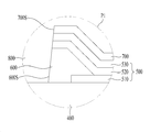
도 1은 본 발명의 실시 예에 따른 유기 발광 표시 장치의 단면을 나타낸 도면이다.
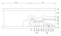
도 2는 도 1의 P1 영역을 확대한 도면이다.
도 3은 본 발명의 다른 실시 예에 따른 유기 발광 표시 장치의 일부 영역을 확대한 도면이다.
도 4는 본 발명의 다른 실시 예에 따른 유기 발광 표시 장치의 단면을 나타낸 도면이다.
도 5는 도 4의 P2 영역을 확대한 도면이다.
도 6은 본 발명의 또다른 실시 예에 따른 유기 발광 표시 장치의 일부 영역을 확대한 도면이다.FIG. 1 is a cross-sectional view of an OLED display according to an embodiment of the present invention. Referring to FIG.
2 is an enlarged view of the region P1 in Fig.
3 is an enlarged view of a part of an organic light emitting display according to another embodiment of the present invention.
4 is a cross-sectional view of an OLED display according to another embodiment of the present invention.
5 is an enlarged view of the region P2 in Fig.
6 is an enlarged view of a part of an organic light emitting display according to another embodiment of the present invention.
본 발명의 상기 목적과 기술적 구성 및 이에 따른 작용 효과에 관한 자세한 사항은 본 발명의 실시 예를 도시하고 있는 도면을 참조한 이하 상세한 설명에 의해 더욱 명확하게 이해될 것이다. 여기서, 본 발명의 실시 예들은 당업자에게 본 발명의 기술적 사상이 충분히 전달될 수 있도록 하기 위하여 제공되는 것이므로, 본 발명은 이하 설명되는 실시 예들에 한정되지 않도록 다른 형태로 구체화될 수 있다.DETAILED DESCRIPTION OF THE PREFERRED EMBODIMENTS Reference will now be made in detail to the preferred embodiments of the present invention, examples of which are illustrated in the accompanying drawings, wherein like reference numerals refer to the like elements throughout. Hereinafter, exemplary embodiments of the present invention will be described in detail with reference to the accompanying drawings. In the following description, well-known functions or constructions are not described in detail since they would obscure the invention in unnecessary detail.
또한, 명세서 전체에 걸쳐서 동일한 참조 번호로 표시된 부분들은 동일한 구성 요소들을 의미하며, 도면들에 있어서 층 또는 영역의 길이와 두께는 편의를 위하여 과장되어 표현될 수 있다. 덧붙여, 제 1 구성 요소가 제 2 구성 요소 "상"에 있다고 기재되는 경우, 상기 제 1 구성 요소가 상기 제 2 구성 요소와 직접 접촉하는 상측에 위치하는 것뿐만 아니라, 상기 제 1 구성 요소와 상기 제 2 구성 요소 사이에 제 3 구성 요소가 위치하는 경우도 포함한다.In the drawings, the same reference numerals denote the same components throughout the specification. In the drawings, the lengths and the thicknesses of layers or regions may be exaggerated for convenience. In addition, when the first component is described as being on the second component, it is preferable that the first component is located on the upper side in direct contact with the second component, And the third component is located between the second components.
여기서, 상기 제 1, 제 2 등의 용어는 다양한 구성 요소를 설명하기 위한 것으로, 하나의 구성 요소를 다른 구성 요소로부터 구별하는 목적으로 사용된다. 다만, 본 발명의 기술적 사상을 벗어나지 않는 범위에서는 제 1 구성 요소와 제 2 구성 요소는 당업자의 편의에 따라 임의로 명명될 수 있다.Here, the terms first, second, etc. are used for describing various components and are used for the purpose of distinguishing one component from another component. However, the first component and the second component may be arbitrarily named according to the convenience of the person skilled in the art without departing from the technical idea of the present invention.
본 발명의 명세서에서 사용하는 용어는 단지 특정한 실시 예를 설명하기 위해 사용되는 것으로, 본 발명을 한정하려는 의도가 아니다. 예를 들어, 단수로 표현된 구성 요소는 문맥상 명백하게 단수만을 의미하지 않는다면 복수의 구성 요소를 포함한다. 또한, 본 발명의 명세서에서, "포함하다" 또는 "가지다"등의 용어는 명세서 상에 기재된 특징, 숫자, 단계, 동작, 구성 요소, 부분품 또는 이들을 조합한 것이 존재함을 지정하려는 것이지, 하나 또는 그 이상의 다른 특징들이나 숫자, 단계, 동작, 구성 요소, 부분품 또는 이들을 조합한 것들의 존재 또는 부가 가능성을 미리 배제하지 않는 것으로 이해되어야 한다.It is to be understood that the terminology used herein is for the purpose of describing particular embodiments only and is not intended to be limiting of the invention. For example, an element represented in singular form includes a plurality of elements unless the context clearly dictates a singular number. Also, in the specification of the present invention, the terms such as " comprises "or" having ", and the like, designate the presence of stated features, integers, steps, operations, elements, But do not preclude the presence or addition of one or more other features, numbers, steps, operations, components, parts, or combinations thereof.
덧붙여, 다르게 정의되지 않는 한, 기술적이거나 과학적인 용어를 포함해서 여기서 사용되는 모든 용어들은 본 발명이 속하는 기술 분야에서 통상의 지식을 가진 자에 의해 일반적으로 이해되는 것과 동일한 의미가 있다. 일반적으로 사용되는 사전에 정의되어 있는 것과 같은 용어들은 관련 기술의 문맥상 가지는 의미와 일치하는 의미가 있는 것으로 해석되어야 하며, 본 발명의 명세서에서 명백하게 정의하지 않는 한, 이상적이거나 과도하게 형식적인 의미로 해석되지 않는다.In addition, unless otherwise defined, all terms used herein, including technical or scientific terms, have the same meaning as commonly understood by one of ordinary skill in the art to which this invention belongs. Terms such as those defined in commonly used dictionaries are to be interpreted as having a meaning consistent with the meaning in the context of the related art and, unless expressly defined in the specification of the present invention, are intended to mean either an ideal or an overly formal meaning It is not interpreted.
(실시 예)(Example)
도 1은 본 발명의 실시 예에 따른 유기 발광 표시 장치의 단면을 나타낸 도면이다. 도 2는 도 1의 P1 영역을 확대한 도면이다.FIG. 1 is a cross-sectional view of an OLED display according to an embodiment of the present invention. Referring to FIG. 2 is an enlarged view of the region P1 in Fig.
도 1 및 2를 참조하면, 본 발명의 실시 예에 따른 유기 발광 표시 장치는 하부 기판(100), 상부 기판(200), 박막 트랜지스터(300), 평탄화막(400), 발광 구조물(500), 뱅크 절연막(600), 보호막(800) 및 접착층(900)을 포함할 수 있다.1 and 2, an OLED display according to an exemplary embodiment of the present invention includes a
상기 하부 기판(100)은 상기 박막 트랜지스터(300) 및 상기 발광 구조물(500)을 지지할 수 있다. 상기 하부 기판(100)은 표시 영역(AA) 및 비표시 영역(NA)을 포함할 수 있다. 상기 비표시 영역(NA)은 상기 표시 영역(AA)의 외측에 위치할 수 있다. 예를 들어, 상기 비표시 영역(NA)은 상기 하부 기판(100)의 가장 자리 측면에 가까이 위치할 수 있다. The
상기 하부 기판(100)은 절연성 물질을 포함할 수 있다. 상기 하부 기판(100)은 투명성 물질을 포함할 수 있다. 예를 들어, 상기 하부 기판(100)은 유리 또는 플라스틱을 포함할 수 있다.The
상기 상부 기판(200)은 상기 하부 기판(100) 상에 위치할 수 있다. 상기 상부 기판(200)은 상기 하부 기판(100)의 상기 표시 영역(AA) 및 상기 비표시 영역(NA)과 수직 중첩할 수 있다.The
상기 상부 기판(200)은 금속 물질을 포함할 수 있다. 예를 들어, 상기 상부 기판(200)은 알루미늄 또는 구리를 포함할 수 있다. The
상기 박막 트랜지스터(300)는 상기 하부 기판(100)과 상기 상부 기판(200) 사이에 위치할 수 있다. 예를 들어, 상기 박막 트랜지스터(300)는 상기 상부 기판(200)을 향한 상기 하부 기판(100)의 상기 표시 영역(AA)의 표면 상에 위치할 수 있다. The
본 발명의 실시 예에 따른 유기 발광 표시 장치는 박막 트랜지스터(300)가 하부 기판(100)과 직접 접촉하는 것으로 설명된다. 그러나, 본 발명의 다른 실시 예에 따른 유기 발광 표시 장치는 하부 기판(100)과 박막 트랜지스터(300) 사이에 위치하는 버퍼층을 더 포함할 수 있다. 상기 버퍼층은 절연성 물질을 포함할 수 있다. 예를 들어, 상기 버퍼층은 실리콘 산화물 및/또는 실리콘 질화물을 포함할 수 있다. The organic light emitting diode display according to the embodiment of the present invention is described in which the
상기 박막 트랜지스터(300)는 소스 영역, 드레인 영역 및 채널 영역을 포함하는 반도체층(310), 상기 반도체층(310)의 상기 채널 영역과 수직 중첩하는 게이트 전극(330), 상기 반도체층(310)과 상기 게이트 전극(330) 사이에 위치하는 게이트 절연막(320), 상기 반도체층(310)의 상기 드레인 영역과 연결되는 드레인 전극(350), 상기 반도체층(310)의 상기 소스 영역과 연결되는 소스 전극(360) 및 상기 게이트 전극(330)과 상기 드레인 전극(350) 및 상기 소스 전극(360) 사이에 위치하는 층간 절연막(340)을 포함할 수 있다. The
상기 반도체층(310)은 반도체 물질을 포함할 수 있다. 예를 들어, 상기 반도체층(310)은 비정질 실리콘 또는 다결정 실리콘을 포함할 수 있다.The
상기 게이트 전극(330), 상기 드레인 전극(350) 및 상기 소스 전극(360)은 도전성 물질을 포함할 수 있다. 예를 들어, 상기 게이트 전극(330), 상기 드레인 전극(350) 및 상기 소스 전극(360)은 금속을 포함할 수 있다. 상기 소스 전극(360)은 상기 드레인 전극(350)과 동일한 물질을 포함할 수 있다. 상기 게이트 전극(330)은 상기 드레인 전극(350) 및 상기 소스 전극(360)과 다른 물질을 포함할 수 있다. The
상기 게이트 절연막(320) 및 상기 층간 절연막(340)은 절연성 물질을 포함할 수 있다. 상기 게이트 절연막(320)의 측면은 상기 게이트 전극(330)의 측면과 수직 정렬될 수 있다. 상기 층간 절연막(340)은 상기 하부 기판(100)의 상기 표시 영역(AA)을 전체적으로 덮을 수 있다. The
본 발명의 실시 예에 따른 유기 발광 표시 장치는 박막 트랜지스터(300)가 반도체층(310)의 상부면 상에 위치하는 게이트 전극(330)을 포함하는 것으로 설명된다. 그러나, 본 발명의 다른 실시 예에 따른 유기 발광 표시 장치는 게이트 전극(330)의 상부면 상에 반도체층(310)이 위치하는 박막 트랜지스터(300)를 포함할 수 있다. An organic light emitting display according to an embodiment of the present invention is described as including a
상기 평탄화막(400)은 상기 박막 트랜지스터(300)에 의한 단차를 제거할 수 있다. 예를 들어, 상기 평탄화막(400)의 상부면은 상기 하부 기판(100)의 표면과 평행할 수 있다.The
상기 평탄화막(400)은 상기 하부 기판(100)의 상기 표시 영역(AA)을 전체적으로 덮을 수 있다. 예를 들어, 상기 평탄화막(400)은 상기 층간 절연막(340)의 상부면과 직접 접촉할 수 있다. 상기 드레인 전극(350) 및 상기 소스 전극(360)은 상기 평탄화막(400)에 의해 덮일 수 있다.The
상기 평탄화막(400)은 절연성 물질을 포함할 수 있다. 예를 들어, 상기 평탄화막(400)은 실리콘 산화물을 포함할 수 있다.The
상기 발광 구조물(500)은 특정 색을 구현하는 빛을 생성할 수 있다. 상기 발광 구조물(500)은 상기 하부 기판(100)의 상기 표시 영역(AA) 상에 위치할 수 있다. 예를 들어, 상기 발광 구조물(500)은 상기 평탄화막(400)과 상기 상부 기판(200) 사이에 위치할 수 있다.The
상기 발광 구조물(500)은 순서대로 적층된 하부 전극(510), 유기 발광층(520) 및 상부 전극(530)을 포함할 수 있다. 상기 하부 전극(510)은 상기 박막 트랜지스터(300)와 전기적으로 연결될 수 있다. 예를 들어, 상기 평탄화막(400)은 상기 박막 트랜지스터(300)의 상기 드레인 전극(350)을 부분적으로 노출하는 콘택홀을 포함할 수 있다. The
상기 하부 전극(510) 및 상기 상부 전극(530)은 도전성 물질을 포함할 수 있다. 상기 상부 전극(530)은 상기 하부 전극(510)과 다른 물질을 포함할 수 있다. 상기 하부 전극(510) 및 상기 상부 전극(530) 중 하나는 투명한 물질을 포함할 수 있다. 예를 들어, 상기 하부 전극(510)은 ITO 또는 IZO를 포함할 수 있다. 상기 상부 전극(530)은 금속을 포함할 수 있다. 상기 상부 전극(530)은 반사율이 높은 물질을 포함할 수 있다. 예를 들어, 상기 상부 전극(530)은 알루미늄을 포함할 수 있다. The
상기 하부 전극(520)은 인접한 화소 영역에서 분리될 수 있다. 상기 상부 전극(530)은 인접한 화소 영역에서 연결될 수 있다. 예를 들어, 각각의 화소 영역에서 구현되는 색의 휘도는 상기 하부 전극(520)에 인가되는 전압 및 전류를 통해 조절될 수 있다. The
본 발명의 실시 예에 따른 유기 발광 표시 장치는 상부 기판(200) 및 상부 전극(530)이 금속을 포함하는 바텀 에미션 방식인 것으로 설명된다. 그러나 본 발명의 다른 실시 예에 따른 유기 발광 표시 장치는 탑 에미션 방식일 수 있다. 예를 들어, 본 발명의 다른 실시 예에 따른 유기 발광 표시 장치는 상기 상부 기판(200) 및 상기 상부 전극(530)이 투명한 물질을 포함할 수 있다.The organic light emitting display according to the embodiment of the present invention is described as being a bottom emission type in which the
상기 유기 발광층(520)은 상기 하부 전극(510)과 상기 상부 전극(530) 사이의 전압 차에 대응하는 휘도의 빛을 생성할 수 있다. 상기 유기 발광층(520)에 의해 생성된 빛은 특정 색을 구현할 수 있다. 예를 들어, 각각의 화소 영역에서 상기 유기 발광층(520)에 의해 생성된 빛은 적색, 녹색, 청색 및 백색 중 하나를 구현할 수 있다. 상기 유기 발광층(520)은 인접한 화소 영역에서 분리될 수 있다. 인접한 화소 영역에 위치하는 상기 유기 발광층(520)은 서로 다른 색을 구현할 수 있다. The organic
상기 유기 발광층(520)은 유기 발광 물질을 함유하는 발광 물질층(Emitting Material Layer)을 포함할 수 있다. 상기 유기 발광층(520)은 발광 효율을 높이기 위하여 다층 구조일 수 있다. 예를 들어, 상기 유기 발광층(520)은 정공 주입층(Hole Injection Layer; HIL), 정공 수송층(Hole Transporting Layer; HTL), 전자 수송층(Electron Transporting Layer; ETL) 및 전자 주입층(Electron Injection Layer; EIL) 중 적어도 하나를 포함할 수 있다. The organic
상기 유기 발광층(520)의 측면은 상기 하부 기판(100)의 상기 표시 영역(AA) 내에 위치할 수 있다. 예를 들어, 상기 유기 발광층(520)은 마스크를 이용한 유기 물질의 증착 공정 및 상기 하부 기판(100)의 상기 비표시 영역(NA) 상에 증착된 유기 물질을 제거하는 유기물 애싱 공정(organic ahsing process)이 순차적으로 수행되어 형성될 수 있다. The side surface of the organic
본 발명의 실시 예에 따른 유기 발광 표시 장치는 발광 구조물(500)의 유기 발광층(520)이 하부 기판(100)의 표시 영역(AA) 상에만 위치할 수 있다. 따라서, 본 발명의 실시 예에 따른 유기 발광 표시 장치에서는 증착 쉐도우에 의해 상기 유기 발광층(520)이 투습 경로로 작용하는 것이 방지될 수 있다. The organic
상기 하부 기판(100)의 상기 비표시 영역(NA)을 향한 상기 유기 발광층(520)의 측면은 상기 하부 기판(100)의 상기 비표시 영역(NA)을 향한 상기 상부 전극(530)의 측면과 연속될 수 있다. 상기 유기 발광층(520)은 상기 상부 전극(530)의 측면과 수직 정렬되는 측면을 포함할 수 있다. 예를 들어, 상기 유기 발광층(520)을 형성하기 위한 유기물 애싱 공정은 상기 상부 전극(530)를 패터닝하기 위한 마스크를 이용하여 수행될 수 있다. A side surface of the organic
상기 뱅크 절연막(600)은 인접한 화소 영역에 위치하는 상기 하부 전극(510) 사이를 절연할 수 있다. 예를 들어, 상기 뱅크 절연막(600)은 각 화소 영역에 위치하는 상기 하부 전극(510)의 가장 자리를 덮을 수 있다. 상기 유기 발광층(520)은 상기 뱅크 절연막(600) 상으로 연장할 수 있다. 예를 들어, 인접한 화소 영역에서 분리되는 상기 유기 발광층(520)의 측면은 상기 뱅크 절연막(600) 상에 위치할 수 있다. The
상기 뱅크 절연막(600)은 절연성 물질을 포함할 수 있다. 상기 뱅크 절연막(600)은 유기 물질을 포함할 수 있다. 예를 들어, 상기 뱅크 절연막(600)은 벤소사이클로부텐(BCB), 폴리 이미드(poly-imide) 및 포토 아크릴(photo-acryl) 중 하나를 포함할 수 있다. The
상기 하부 기판(100)의 상기 비표시 영역(NA)을 향한 상기 뱅크 절연막(600)의 측면(600s)은 상기 하부 기판(100)의 상기 표시 영역(AA) 상에 위치할 수 있다. 예를 들어, 상기 뱅크 절연막(600)은 마스크를 이용한 유기 물질의 증착 공정 및 상기 하부 기판(100)의 상기 비표시 영역(NA) 상에 증착된 유기 물질을 제거하는 유기물 애싱 공정이 순차적으로 수행되어 형성될 수 있다.The side face 600s of the
본 발명의 실시 예에 따른 유기 발광 표시 장치는 뱅크 절연막(600)이 하부 기판(100)의 표시 영역(AA) 상에만 위치할 수 있다. 따라서, 본 발명의 실시 예에 따른 유기 발광 표시 장치에서는 증착 쉐도우에 의해 상기 뱅크 절연막(600)이 투습 경로로 작용하는 것이 방지될 수 있다. In the organic light emitting diode display according to the embodiment of the present invention, the
상기 하부 기판(100)의 상기 비표시 영역(NA)을 향한 상기 뱅크 절연막(600)의 측면(600s)은 상기 하부 기판(100)의 상기 비표시 영역(NA)을 향한 상기 유기 발광층(520)의 측면과 수직 정렬될 수 있다. 예를 들어, 상기 하부 기판(100)의 상기 비표시 영역(NA)을 향한 상기 뱅크 절연막(600)의 측면(600s)은 상기 유기 발광층(520)의 측면과 연속될 수 있다. 증착 쉐도우에 의해 상기 하부 기판(100)의 상기 비표시 영역(NA) 상에 형성된 상기 유기 발광층(520) 및 상기 뱅크 절연막(600)은 동시에 제거될 수 있다. 예를 들어, 상기 하부 기판(100) 상에 뱅크 절연막(600)을 형성하기 위한 유기 물질 및 상기 유기 발광층(520)을 형성하기 위한 유기 물질을 증착하고, 상기 상부 전극(530)를 패터닝하기 위한 마스크를 이용한 유기물 애싱 공정을 통해 상기 하부 기판(100)의 상기 비표시 영역(NA) 상에 형성된 상기 유기 발광층(520) 및 상기 뱅크 절연막(600)을 제거함으로써, 상기 유기 발광층(520) 및 상기 뱅크 절연막(600)을 동시에 형성할 수 있다. 따라서, 본 발명의 실시 예에 따른 유기 발광 표시 장치는 상부 전극(530)를 패터닝하기 위한 마스크를 이용하여 하부 기판(100)의 비표시 영역(NA) 상에 형성된 유기 발광층(520) 및 뱅크 절연막(600)을 제거함으로써, 제조 비용을 절감할 수 있다. The side surfaces 600s of the
상기 보호막(800)은 외부의 수분이 상기 발광 구조물(500)로 침투하는 것을 방지할 수 있다. 예를 들어, 상기 보호막(800)은 투습 방지 효과가 높은 무기 물질을 포함할 수 있다. The
상기 보호막(800)은 상기 발광 구조물(500) 상에 위치할 수 있다. 상기 보호막(800)은 상기 하부 기판(100)의 상기 비표시 영역(NA) 상으로 연장할 수 있다. 상기 발광 구조물(500)의 측면은 상기 보호막(800)에 의해 덮일 수 있다. 예를 들어, 상기 하부 기판(100)의 상기 비표시 영역(NA)을 향한 상기 뱅크 절연막(600)의 측면(600s)은 상기 보호막(800)과 직접 접촉할 수 있다. The
상기 접착층(900)은 상기 보호막(800) 상에 위치할 수 있다. 상기 접착층(900)은 상기 하부 기판(100)의 상기 비표시 영역(NA) 상으로 연장할 수 있다. 상기 접착층(900)은 상기 하부 기판(100)의 가장 자리 측면(100e)에 가까이 위치하는 상기 하부 기판(100)의 상기 비표시 영역(NA)과 직접 접촉할 수 있다. 상기 상부 기판(200)은 상기 접착층(900)에 의해 상기 발광 구조물(500)이 형성된 상기 하부 기판(100)에 부착될 수 있다. The
본 발명의 실시 예에 따른 유기 발광 표시 장치는 증착 쉐도우에 의해 하부 기판(100)의 비표시 영역(NA) 상에 형성된 유기 발광층(520) 및 뱅크 절연막(600)을 제거함으로써, 상기 유기 발광층(520) 및 상기 뱅크 절연막(600)이 상기 하부 기판(100)의 표시 영역(AA) 상에만 위치할 수 있다. 따라서, 본 발명의 실시 예에 따른 유기 발광 표시 장치에서는 증착 쉐도우에 의해 상기 유기 발광층(520) 및 상기 뱅크 절연막(600)이 투습 경로로 작용하는 것이 방지될 수 있다. 또한, 본 발명의 실시 예에 따른 유기 발광 표시 장치에서는 증착 쉐도우에 의해 하부 기판(100)과 접착층(900) 사이의 접합 면적이 감소하는 것이 방지될 수 있다.The organic light emitting display according to the embodiment of the present invention can remove the organic
본 발명의 실시 예에 따른 유기 발광 표시 장치에서는 발광 구조물(500)의 상부면과 보호막(800) 사이에 위치하는 캡핑층(700)을 더 포함할 수 있다. 상기 캡핑층(700)은 상기 발광 구조물(500)의 상기 상부 전극(530)의 손상을 방지할 수 있다. 예를 들어, 상기 상부 전극(530)의 상부면은 상기 캡핑층(700)에 의해 덮일 수 있다. The organic light emitting diode display according to an embodiment of the present invention may further include a
상기 캡핑층(700)은 절연성 물질을 포함할 수 있다. 예를 들어, 상기 캡핑층(700)은 유기 물질을 포함할 수 있다. The
상기 하부 기판(100)의 상기 비표시 영역(NA)을 향한 상기 캡핑층(700)의 측면(700s)은 상기 하부 기판(100)의 상기 표시 영역(AA) 내에 위치할 수 있다. 예를 들어, 상기 캡핑층(700)은 마스크를 이용한 유기 물질의 증착 공정 및 상기 하부 기판(100)의 상기 비표시 영역(NA) 상에 증착된 유기 물질을 제거하는 유기물 애싱 공정이 순차적으로 수행되어 형성될 수 있다.The side 700s of the
본 발명의 실시 예에 따른 유기 발광 표시 장치는 유기 물질로 형성된 캡핑층(700)이 하부 기판(100)의 표시 영역(AA) 상에만 위치할 수 있다. 따라서, 본 발명의 실시 예에 따른 유기 발광 표시 장치에서는 증착 쉐도우에 의해 상기 캡핑층(700)이 투습 경로로 작용하는 것이 방지될 수 있다. An organic light emitting display according to an embodiment of the present invention may include a
결과적으로 본 발명의 실시 예에 따른 유기 발광 표시 장치는 증착 쉐도우에 의해 하부 기판(100)의 비표시 영역(NA) 상에 증착된 유기 물질을 제거함으로써, 증착 쉐도우에 의한 수분의 침투를 방지하고, 하부 기판(100)이 접착층(900)과 충분히 접촉되도록 할 수 있다.As a result, the organic light emitting display according to the embodiment of the present invention can prevent the penetration of moisture by the deposition shadow by removing the organic material deposited on the non-display area NA of the
상기 하부 기판(100)의 상기 비표시 영역(NA)을 향한 상기 캡핑층(700)의 측면(700s)은 상기 하부 기판(100)의 상기 비표시 영역(NA)을 향한 상기 상부 전극(530)의 측면과 수직 정렬될 수 있다. 상기 하부 기판(100)의 상기 비표시 영역(NA)을 향한 상기 캡핑층(700)의 측면(700s)은 상기 상부 전극의 측면과 연속될 수 있다. 예를 들어, 상기 캡핑층(700)을 형성하기 위한 유기물 애싱 공정은 상기 상부 전극(530)를 패터닝하기 위한 마스크를 이용하여 수행될 수 있다. 따라서, 본 발명의 실시 예에 따른 유기 발광 표시 장치는 증착 쉐도우에 의해 하부 기판(100)의 비표시 영역(NA) 상에 증착된 유기 물질을 동일한 마스크를 이용하여 제거함으로써, 제조 비용을 절감할 수 있다. The side surface 700s of the
본 발명의 실시 예에 따른 유기 발광 표시 장치는 하부 기판(100)의 비표시 영역(NA)을 향한 캡핑층(700)의 측면(700s)이 상기 하부 기판(100)의 상기 비표시 영역(NA)을 향한 상부 전극(530)의 측면과 수직 정렬되는 것으로 설명된다. 그러나, 도 3에 도시된 바와 같이, 본 발명의 다른 실시 예에 따른 유기 발광 표시 장치는 상기 캡핑층(700)이 상기 상부 전극(530)의 상부면을 부분적으로 노출할 수 있다. 이에 따라 본 발명의 다른 실시 예에 따른 유기 발광 표시 장치에서는 공정 오차에 의해 캡핑층(700)이 하부 기판(100)의 비표시 영역(NA)을 향한 발광 구조물(500)의 측면 상으로 연장되어, 유기 발광층(520) 및/또는 뱅크 절연막(600)과 접촉함으로써, 상기 유기 발광층(520)으로의 투습 경로가 생성되는 것을 방지할 수 있다. The organic light emitting display according to the exemplary embodiment of the present invention includes a
본 발명의 실시 예에 따른 유기 발광 표시 장치는 하부 기판(100)의 비표시 영역(NA)을 향한 뱅크 절연막(600)의 측면(600s)이 하부 기판(100)의 비표시 영역(NA)을 향한 상부 전극(530)의 측면과 수직 정렬되는 것으로 설명된다. 그러나, 도 4 및 5에 도시된 바와 같이, 본 발명의 다른 실시 예에 따른 유기 발광 표시 장치는 상부 전극(530)이 하부 기판(100)의 비표시 영역(NA)을 향한 유기 절연막(520)의 측면 및 뱅크 절연막(600)의 측면(600s) 상으로 연장할 수 있다. 이에 따라 본 발명의 다른 실시 예에 따른 유기 발광 표시 장치에서는 보호막(800)의 결함을 통해 침투한 수분이 상기 유기 발광층(520)으로 이동하는 것을 방지할 수 있다. The organic light emitting display according to the exemplary embodiment of the present invention includes a
덧붙여, 도 4 및 5을 참조하는 본 발명의 다른 실시 예에 따른 유기 발광 표시 장치는 하부 기판(100)의 비표시 영역(NA)을 향한 캡핑층(700)의 측면(700s)이 상기 뱅크 절연막(600)의 측면(600s) 상에 위치하는 상부 전극(530)의 표면과 수직 정렬되는 것으로 설명된다. 그러나, 도 6에 도시된 바와 같이, 본 발명의 또다른 실시 예에 따른 유기 발광 표시 장치는 캡핑층(700)이 상부 전극(530)의 상부면을 부분적으로 노출할 수 있다. 예를 들어, 본 발명의 또다른 실시 예에 따른 유기 발광 표시 장치에서 하부 기판(100)의 비표시 영역(NA)을 향한 캡핑층(700)의 측면(700s)은 상기 하부 기판(100)의 상기 비표시 영역(NA)을 향한 뱅크 절연막(600)의 측면(600s)과 수직 정렬될 수 있다. 즉, 본 발명의 또다른 실시 예에 따른 유기 발광 표시 장치에서는 유기 물질로 형성된 유기 발광층(520), 뱅크 절연막(600) 및 캡핑층(700)이 동일한 마스크를 이용한 유기물 애싱 공정에 의해 형성될 수 있다. 따라서, 본 발명의 또다른 실시 예에 따른 유기 발광 표시 장치에서는 증착 쉐도우에 의해 하부 기판(100)의 비표시 영역(NA) 상에 증착된 유기 물질들을 제거하기 위한 비용을 절감할 수 있다.4 and 5, the side surface 700s of the
100 : 하부 기판 200 : 상부 기판
300 : 박막 트랜지스터 500 : 발광 구조물
520 : 유기 발광층 600 : 뱅크 절연막
700 : 캡핑층100: lower substrate 200: upper substrate
300: thin film transistor 500: light emitting structure
520: organic light emitting layer 600: bank insulating film
700: capping layer
Claims (9)
상기 하부 전극의 가장 자리를 덮는 뱅크 절연막;
상기 하부 전극 상에 위치하고, 상기 뱅크 절연막 상으로 연장하는 유기 발광층; 및
상기 유기 발광층 상에 위치하는 상부 전극을 포함하되,
상기 뱅크 절연막은 상기 유기 발광층의 측면과 수직 정렬되는 측면을 포함하는 유기 발광 표시 장치.A lower electrode positioned on the lower substrate;
A bank insulating film covering the edge of the lower electrode;
An organic emission layer disposed on the lower electrode and extending on the bank insulation layer; And
And an upper electrode positioned on the organic light emitting layer,
Wherein the bank insulating layer includes a side surface that is vertically aligned with a side surface of the organic light emitting layer.
상기 상부 전극은 상기 유기 발광층의 측면과 수직 정렬되는 측면을 포함하는 유기 발광 표시 장치. The method according to claim 1,
Wherein the upper electrode includes a side surface that is vertically aligned with a side surface of the organic light emitting layer.
상기 상부 전극의 상부면 상에 위치하는 캡핑층; 및
상기 캡핑층 상에 위치하고, 상기 뱅크 절연막의 상기 측면 상으로 연장하는 보호막을 더 포함하는 유기 발광 표시 장치.The method according to claim 1,
A capping layer located on an upper surface of the upper electrode; And
And a protective layer disposed on the capping layer and extending on the side surface of the bank insulating layer.
상기 캡핑층은 상기 상부 전극의 상기 측면과 수직 정렬되는 측면을 포함하는 유기 발광 표시 장치. The method of claim 3,
Wherein the capping layer includes a side surface that is vertically aligned with the side surface of the upper electrode.
상기 하부 기판의 상기 표시 영역 상에 위치하고, 순서대로 적층된 하부 전극, 유기 발광층 및 상부 전극을 포함하는 발광 구조물; 및
상기 하부 전극의 가장 자리와 상기 유기 발광층 사이에 위치하고, 상기 하부 전극의 외측 방향으로 연장하는 뱅크 절연막을 포함하되,
상기 하부 기판의 상기 비표시 영역을 향한 상기 뱅크 절연막의 측면은 상기 하부 기판의 상기 비표시 영역을 향한 상기 유기 발광층의 측면과 연속되는 유기 발광 표시 장치.A lower substrate including a display region and a non-display region located outside the display region;
A light emitting structure disposed on the display region of the lower substrate and including a lower electrode, an organic light emitting layer, and an upper electrode sequentially stacked; And
And a bank insulating layer disposed between the edge of the lower electrode and the organic light emitting layer and extending in an outward direction of the lower electrode,
And the side surfaces of the bank insulating film toward the non-display region of the lower substrate are continuous with the side surfaces of the organic light emitting layer toward the non-display region of the lower substrate.
상기 하부 기판의 상기 비표시 영역을 향한 상기 뱅크 절연막의 측면 및 상기 유기 발광층의 측면은 상기 하부 기판의 상기 표시 영역 내에 위치하는 유기 발광 표시 장치.6. The method of claim 5,
And a side surface of the bank insulating film and a side surface of the organic light emitting layer facing the non-display region of the lower substrate are positioned within the display region of the lower substrate.
상기 상부 전극은 상기 하부 기판의 상기 비표시 영역을 향한 상기 뱅크 절연막의 측면 상으로 연장하는 유기 발광 표시 장치.6. The method of claim 5,
Wherein the upper electrode extends on a side surface of the bank insulating film toward the non-display region of the lower substrate.
상기 발광 구조물 상에 위치하고, 상기 하부 기판의 상기 비표시 영역 상으로 연장하는 보호막; 및
상기 상부 전극과 상기 보호막 사이에 위치하는 캡핑층을 더 포함하되,
상기 하부 기판의 상기 비표시 영역을 향한 상기 캡핑층의 측면은 상기 상부 전극의 상부면 상에 위치하는 유기 발광 표시 장치. 8. The method of claim 7,
A protective film on the light emitting structure and extending onto the non-display area of the lower substrate; And
And a capping layer disposed between the upper electrode and the passivation layer,
And a side surface of the capping layer facing the non-display region of the lower substrate is positioned on an upper surface of the upper electrode.
상기 하부 기판의 상기 비표시 영역을 향한 상기 캡핑층의 측면은 상기 하부 기판의 상기 비표시 영역을 향한 상기 유기 발광층의 측면과 수직 정렬되는 유기 발광 표시 장치. 9. The method of claim 8,
And a side surface of the capping layer facing the non-display area of the lower substrate is vertically aligned with a side surface of the organic light emitting layer toward the non-display area of the lower substrate.
Priority Applications (6)
| Application Number | Priority Date | Filing Date | Title |
|---|---|---|---|
| KR1020160067738A KR20170135585A (en) | 2016-05-31 | 2016-05-31 | Organic Light Emitting Display device having a bank insulating layer |
| CN201710228676.XA CN107452765B (en) | 2016-05-31 | 2017-04-10 | Organic light emitting display device having bank insulating layer |
| TW106111888A TWI640113B (en) | 2016-05-31 | 2017-04-10 | Organic light-emitting display device having bank insulating layer |
| US15/490,508 US10714546B2 (en) | 2016-05-31 | 2017-04-18 | Organic light-emitting display device having bank insulating layer |
| DE102017110214.0A DE102017110214A1 (en) | 2016-05-31 | 2017-05-11 | Organic light-emitting display device with a bank insulating layer |
| KR1020230189942A KR20240005634A (en) | 2016-05-31 | 2023-12-22 | Organic Light Emitting Display device having a bank insulating layer |
Applications Claiming Priority (1)
| Application Number | Priority Date | Filing Date | Title |
|---|---|---|---|
| KR1020160067738A KR20170135585A (en) | 2016-05-31 | 2016-05-31 | Organic Light Emitting Display device having a bank insulating layer |
Related Child Applications (1)
| Application Number | Title | Priority Date | Filing Date |
|---|---|---|---|
| KR1020230189942A Division KR20240005634A (en) | 2016-05-31 | 2023-12-22 | Organic Light Emitting Display device having a bank insulating layer |
Publications (1)
| Publication Number | Publication Date |
|---|---|
| KR20170135585A true KR20170135585A (en) | 2017-12-08 |
Family
ID=60268690
Family Applications (2)
| Application Number | Title | Priority Date | Filing Date |
|---|---|---|---|
| KR1020160067738A KR20170135585A (en) | 2016-05-31 | 2016-05-31 | Organic Light Emitting Display device having a bank insulating layer |
| KR1020230189942A KR20240005634A (en) | 2016-05-31 | 2023-12-22 | Organic Light Emitting Display device having a bank insulating layer |
Family Applications After (1)
| Application Number | Title | Priority Date | Filing Date |
|---|---|---|---|
| KR1020230189942A KR20240005634A (en) | 2016-05-31 | 2023-12-22 | Organic Light Emitting Display device having a bank insulating layer |
Country Status (5)
| Country | Link |
|---|---|
| US (1) | US10714546B2 (en) |
| KR (2) | KR20170135585A (en) |
| CN (1) | CN107452765B (en) |
| DE (1) | DE102017110214A1 (en) |
| TW (1) | TWI640113B (en) |
Families Citing this family (1)
| Publication number | Priority date | Publication date | Assignee | Title |
|---|---|---|---|---|
| KR20200082496A (en) * | 2018-12-28 | 2020-07-08 | 엘지디스플레이 주식회사 | Display Device and Method for Manufacturing the Same |
Family Cites Families (20)
| Publication number | Priority date | Publication date | Assignee | Title |
|---|---|---|---|---|
| JP3830238B2 (en) * | 1997-08-29 | 2006-10-04 | セイコーエプソン株式会社 | Active matrix type device |
| JP2001109395A (en) * | 1999-10-01 | 2001-04-20 | Sanyo Electric Co Ltd | El display device |
| JP4001066B2 (en) * | 2002-07-18 | 2007-10-31 | セイコーエプソン株式会社 | Electro-optical device, wiring board, and electronic equipment |
| JP2004200034A (en) * | 2002-12-19 | 2004-07-15 | Seiko Epson Corp | Electro-optical device and its process of manufacture as well as electronic equipment |
| JP4239999B2 (en) * | 2005-05-11 | 2009-03-18 | セイコーエプソン株式会社 | Film pattern forming method, film pattern, device, electro-optical device, and electronic apparatus |
| KR100645706B1 (en) * | 2006-01-27 | 2006-11-15 | 삼성에스디아이 주식회사 | Organic light-emitting display device and method for fabricating the same |
| JP5207670B2 (en) * | 2006-07-19 | 2013-06-12 | キヤノン株式会社 | Display device |
| US8536611B2 (en) * | 2008-06-17 | 2013-09-17 | Hitachi, Ltd. | Organic light-emitting element, method for manufacturing the organic light-emitting element, apparatus for manufacturing the organic light-emitting element, and organic light-emitting device using the organic light-emitting element |
| KR20100036624A (en) * | 2008-09-30 | 2010-04-08 | 삼성전자주식회사 | Thin film transistor substrate and organic light emitting display having the same |
| JP5157825B2 (en) * | 2008-10-29 | 2013-03-06 | ソニー株式会社 | Manufacturing method of organic EL display |
| DE102009037186A1 (en) * | 2009-08-12 | 2011-02-17 | Osram Opto Semiconductors Gmbh | Radiation-emitting semiconductor component |
| KR101084190B1 (en) * | 2010-02-16 | 2011-11-17 | 삼성모바일디스플레이주식회사 | Organic light emitting display and manufacturing method thereof |
| KR20120106453A (en) * | 2011-03-18 | 2012-09-26 | 삼성디스플레이 주식회사 | Organic light emitting diode display |
| KR102028505B1 (en) * | 2012-11-19 | 2019-10-04 | 엘지디스플레이 주식회사 | Organic light-emtting diode display panel and method for fabricating the same |
| JP2015050022A (en) * | 2013-08-30 | 2015-03-16 | 株式会社ジャパンディスプレイ | Organic el display device |
| KR101692351B1 (en) * | 2013-11-27 | 2017-01-03 | 엘지디스플레이 주식회사 | Organic Light Emitting Display Apparatus and Method for Manufacturing The Same |
| KR102255809B1 (en) * | 2013-12-02 | 2021-05-24 | 엘지디스플레이 주식회사 | Organic Light Emitting Display Device |
| KR102201827B1 (en) * | 2014-09-16 | 2021-01-13 | 엘지디스플레이 주식회사 | Organic light emitting display device, organic light emitting display panel and method for fabricating the same |
| KR101640803B1 (en) * | 2014-09-26 | 2016-07-20 | 엘지디스플레이 주식회사 | Organic Light Emitting Diode Display Device and Method of Fabricating the Same |
| KR102295547B1 (en) | 2014-12-03 | 2021-09-01 | 한국전자통신연구원 | Method of fabricating conductive film |
-
2016
- 2016-05-31 KR KR1020160067738A patent/KR20170135585A/en not_active Application Discontinuation
-
2017
- 2017-04-10 TW TW106111888A patent/TWI640113B/en active
- 2017-04-10 CN CN201710228676.XA patent/CN107452765B/en active Active
- 2017-04-18 US US15/490,508 patent/US10714546B2/en active Active
- 2017-05-11 DE DE102017110214.0A patent/DE102017110214A1/en active Pending
-
2023
- 2023-12-22 KR KR1020230189942A patent/KR20240005634A/en not_active Application Discontinuation
Also Published As
| Publication number | Publication date |
|---|---|
| KR20240005634A (en) | 2024-01-12 |
| TW201743485A (en) | 2017-12-16 |
| US20170345879A1 (en) | 2017-11-30 |
| CN107452765A (en) | 2017-12-08 |
| CN107452765B (en) | 2020-08-18 |
| TWI640113B (en) | 2018-11-01 |
| DE102017110214A1 (en) | 2017-11-30 |
| US10714546B2 (en) | 2020-07-14 |
Similar Documents
| Publication | Publication Date | Title |
|---|---|---|
| US11895886B2 (en) | Display device with insulating layer in through hole or notch | |
| KR102456072B1 (en) | Organic light emitting display apparatus and the fabrication method thereof | |
| KR20220147054A (en) | Stretchable display device | |
| US9490311B2 (en) | Organic light emitting display device and method of manufacturing the same | |
| US8822998B2 (en) | Organic light emitting display device | |
| KR20180061903A (en) | Display device having a plurality of insulating layer disposed between two electrodes | |
| US11205760B2 (en) | Display device having opening surrounding display region | |
| KR20160100135A (en) | Organic light emitting display apparatus and the fabrication method thereof | |
| KR102649202B1 (en) | Organic Light Emitting Display device having an organic light emitting layer extending a non-display area | |
| KR102612040B1 (en) | Organic Light Emitting Display device having a partition wall | |
| KR20150071538A (en) | Organic light emitting display apparatus and the manufacturing method thereof | |
| US9882168B2 (en) | Organic electroluminescence display device | |
| KR20200083738A (en) | Organic light emitting display device and method of manufacturing organic light emitting display device | |
| KR20170065069A (en) | Thin film transistor array panel and organic light emitting diode display including the same | |
| KR20190080312A (en) | Organic Light-Emitting Display apparatus having a black bank insulating layer | |
| US9947897B2 (en) | Method of manufacturing display device | |
| KR20160091529A (en) | Organic light emitting display device and manufacturing method thereof | |
| KR20150071318A (en) | Method for manufaturing of organic light emitting diode display | |
| KR101084192B1 (en) | An organic light emitting display device | |
| KR20240005634A (en) | Organic Light Emitting Display device having a bank insulating layer | |
| US20150270323A1 (en) | Organic light-emitting display apparatus and manufacturing method thereof | |
| CN111883562A (en) | Display device | |
| KR20180062228A (en) | Organic Light Emitting Display device having an organic light emitting layer | |
| KR20150059196A (en) | Organic light emitting display device and method for manufacturing thereof | |
| US10224509B2 (en) | Display device |
Legal Events
| Date | Code | Title | Description |
|---|---|---|---|
| E902 | Notification of reason for refusal | ||
| E601 | Decision to refuse application | ||
| E601 | Decision to refuse application | ||
| E801 | Decision on dismissal of amendment |