WO2025142301A1 - 樹脂組成物、硬化物、プリプレグ、樹脂シート、積層板、金属箔張積層板、及びプリント配線板 - Google Patents
樹脂組成物、硬化物、プリプレグ、樹脂シート、積層板、金属箔張積層板、及びプリント配線板 Download PDFInfo
- Publication number
- WO2025142301A1 WO2025142301A1 PCT/JP2024/042243 JP2024042243W WO2025142301A1 WO 2025142301 A1 WO2025142301 A1 WO 2025142301A1 JP 2024042243 W JP2024042243 W JP 2024042243W WO 2025142301 A1 WO2025142301 A1 WO 2025142301A1
- Authority
- WO
- WIPO (PCT)
- Prior art keywords
- group
- resin composition
- mass
- resin
- formula
- Prior art date
- Legal status (The legal status is an assumption and is not a legal conclusion. Google has not performed a legal analysis and makes no representation as to the accuracy of the status listed.)
- Pending
Links
Images


Classifications
-
- B—PERFORMING OPERATIONS; TRANSPORTING
- B32—LAYERED PRODUCTS
- B32B—LAYERED PRODUCTS, i.e. PRODUCTS BUILT-UP OF STRATA OF FLAT OR NON-FLAT, e.g. CELLULAR OR HONEYCOMB, FORM
- B32B15/00—Layered products comprising a layer of metal
- B32B15/04—Layered products comprising a layer of metal comprising metal as the main or only constituent of a layer, which is next to another layer of the same or of a different material
- B32B15/08—Layered products comprising a layer of metal comprising metal as the main or only constituent of a layer, which is next to another layer of the same or of a different material of synthetic resin
-
- B—PERFORMING OPERATIONS; TRANSPORTING
- B32—LAYERED PRODUCTS
- B32B—LAYERED PRODUCTS, i.e. PRODUCTS BUILT-UP OF STRATA OF FLAT OR NON-FLAT, e.g. CELLULAR OR HONEYCOMB, FORM
- B32B27/00—Layered products comprising a layer of synthetic resin
- B32B27/18—Layered products comprising a layer of synthetic resin characterised by the use of special additives
- B32B27/20—Layered products comprising a layer of synthetic resin characterised by the use of special additives using fillers, pigments, thixotroping agents
-
- B—PERFORMING OPERATIONS; TRANSPORTING
- B32—LAYERED PRODUCTS
- B32B—LAYERED PRODUCTS, i.e. PRODUCTS BUILT-UP OF STRATA OF FLAT OR NON-FLAT, e.g. CELLULAR OR HONEYCOMB, FORM
- B32B7/00—Layered products characterised by the relation between layers; Layered products characterised by the relative orientation of features between layers, or by the relative values of a measurable parameter between layers, i.e. products comprising layers having different physical, chemical or physicochemical properties; Layered products characterised by the interconnection of layers
- B32B7/02—Physical, chemical or physicochemical properties
- B32B7/025—Electric or magnetic properties
-
- B—PERFORMING OPERATIONS; TRANSPORTING
- B32—LAYERED PRODUCTS
- B32B—LAYERED PRODUCTS, i.e. PRODUCTS BUILT-UP OF STRATA OF FLAT OR NON-FLAT, e.g. CELLULAR OR HONEYCOMB, FORM
- B32B7/00—Layered products characterised by the relation between layers; Layered products characterised by the relative orientation of features between layers, or by the relative values of a measurable parameter between layers, i.e. products comprising layers having different physical, chemical or physicochemical properties; Layered products characterised by the interconnection of layers
- B32B7/02—Physical, chemical or physicochemical properties
- B32B7/027—Thermal properties
-
- C—CHEMISTRY; METALLURGY
- C08—ORGANIC MACROMOLECULAR COMPOUNDS; THEIR PREPARATION OR CHEMICAL WORKING-UP; COMPOSITIONS BASED THEREON
- C08K—Use of inorganic or non-macromolecular organic substances as compounding ingredients
- C08K3/00—Use of inorganic substances as compounding ingredients
- C08K3/18—Oxygen-containing compounds, e.g. metal carbonyls
- C08K3/20—Oxides; Hydroxides
- C08K3/22—Oxides; Hydroxides of metals
-
- C—CHEMISTRY; METALLURGY
- C08—ORGANIC MACROMOLECULAR COMPOUNDS; THEIR PREPARATION OR CHEMICAL WORKING-UP; COMPOSITIONS BASED THEREON
- C08K—Use of inorganic or non-macromolecular organic substances as compounding ingredients
- C08K3/00—Use of inorganic substances as compounding ingredients
- C08K3/18—Oxygen-containing compounds, e.g. metal carbonyls
- C08K3/24—Acids; Salts thereof
-
- C—CHEMISTRY; METALLURGY
- C08—ORGANIC MACROMOLECULAR COMPOUNDS; THEIR PREPARATION OR CHEMICAL WORKING-UP; COMPOSITIONS BASED THEREON
- C08L—COMPOSITIONS OF MACROMOLECULAR COMPOUNDS
- C08L101/00—Compositions of unspecified macromolecular compounds
-
- C—CHEMISTRY; METALLURGY
- C08—ORGANIC MACROMOLECULAR COMPOUNDS; THEIR PREPARATION OR CHEMICAL WORKING-UP; COMPOSITIONS BASED THEREON
- C08L—COMPOSITIONS OF MACROMOLECULAR COMPOUNDS
- C08L35/00—Compositions of homopolymers or copolymers of compounds having one or more unsaturated aliphatic radicals, each having only one carbon-to-carbon double bond, and at least one being terminated by a carboxyl radical, and containing at least one other carboxyl radical in the molecule, or of salts, anhydrides, esters, amides, imides or nitriles thereof; Compositions of derivatives of such polymers
-
- C—CHEMISTRY; METALLURGY
- C08—ORGANIC MACROMOLECULAR COMPOUNDS; THEIR PREPARATION OR CHEMICAL WORKING-UP; COMPOSITIONS BASED THEREON
- C08L—COMPOSITIONS OF MACROMOLECULAR COMPOUNDS
- C08L71/00—Compositions of polyethers obtained by reactions forming an ether link in the main chain; Compositions of derivatives of such polymers
- C08L71/08—Polyethers derived from hydroxy compounds or from their metallic derivatives
- C08L71/10—Polyethers derived from hydroxy compounds or from their metallic derivatives from phenols
- C08L71/12—Polyphenylene oxides
-
- C—CHEMISTRY; METALLURGY
- C08—ORGANIC MACROMOLECULAR COMPOUNDS; THEIR PREPARATION OR CHEMICAL WORKING-UP; COMPOSITIONS BASED THEREON
- C08L—COMPOSITIONS OF MACROMOLECULAR COMPOUNDS
- C08L79/00—Compositions of macromolecular compounds obtained by reactions forming in the main chain of the macromolecule a linkage containing nitrogen with or without oxygen or carbon only, not provided for in groups C08L61/00 - C08L77/00
- C08L79/04—Polycondensates having nitrogen-containing heterocyclic rings in the main chain; Polyhydrazides; Polyamide acids or similar polyimide precursors
-
- H—ELECTRICITY
- H05—ELECTRIC TECHNIQUES NOT OTHERWISE PROVIDED FOR
- H05K—PRINTED CIRCUITS; CASINGS OR CONSTRUCTIONAL DETAILS OF ELECTRIC APPARATUS; MANUFACTURE OF ASSEMBLAGES OF ELECTRICAL COMPONENTS
- H05K1/00—Printed circuits
- H05K1/02—Details
- H05K1/03—Use of materials for the substrate
Definitions
- the present invention relates to a resin composition, a cured product, a prepreg, a resin sheet, a laminate, a metal foil-clad laminate, and a printed wiring board.
- the dielectric loss of an electric signal is proportional to the product of the square root of the relative dielectric constant of the insulating layer that forms the circuit, the dielectric tangent, and the frequency of the electric signal. Therefore, the higher the frequency of the signal used, the greater the dielectric loss.
- An increase in dielectric loss attenuates the electric signal and reduces the reliability of the signal, so in order to suppress this, it is necessary to select a material with a small dielectric tangent for the insulating layer.
- Insulating layers with high dielectric constants and low dielectric loss tangents are formed by dispersing fillers such as ceramic powder and metal powder that has been treated with an insulating process into a resin.
- voids may occur depending on the filler used, which may cause delamination during the manufacture of laminates. This can lead to problems such as deterioration of thermal properties, such as moisture absorption and heat resistance, and dielectric properties (high dielectric constant and low dielectric tangent) in printed wiring boards, etc.
- the insulating layer must have sufficient metal foil peel strength (e.g., copper foil peel strength) when it is made into a metal foil laminate.
- the present invention has been made to solve the above-mentioned problems, and aims to provide a resin composition that has a high dielectric constant and low dielectric tangent, excellent thermal properties, excellent laser processability, and high metal foil peel strength, and is suitable for use in the manufacture of insulating layers for printed wiring boards, and a cured product, prepreg, resin sheet, laminate, metal foil-clad laminate, and printed wiring board obtained using the resin composition.
- the inventors conducted extensive research to solve the above problems of the conventional technology, and discovered that a specific resin composition can solve the problems, which led to the completion of the present invention.
- a resin composition comprising: a dielectric powder (A) having a relative dielectric constant of 12.0 or more at a frequency of 10 GHz measured according to a cavity resonator perturbation method; an inorganic filler (B) different from the dielectric powder (A), which has an absorbance of 0.70 or more at a wavelength of 9.3 ⁇ m in an infrared absorption spectrum obtained using Fourier transform infrared spectroscopy and a melting point of 1600° C. or less; and a thermosetting resin (C).
- thermosetting resin (C) contains at least one selected from the group consisting of maleimide compounds, cyanate ester compounds, epoxy compounds, phenolic compounds, modified polyphenylene ether compounds, alkenyl-substituted nadiimide compounds, oxetane resins, benzoxazine compounds, and compounds having a polymerizable unsaturated group.
- maleimide compound includes at least one selected from the group consisting of bis(4-maleimidophenyl)methane, 2,2-bis(4-(4-maleimidophenoxy)-phenyl)propane, bis(3-ethyl-5-methyl-4-maleimidophenyl)methane, maleimide compounds represented by the following formula (1), maleimide compounds represented by the following formula (2), maleimide compounds represented by the following formula (3), and maleimide compounds represented by the following formula (4).
- each R 1 independently represents a hydrogen atom or a methyl group, and n1 represents an integer of 1 to 10.
- each R 2 independently represents a hydrogen atom, an alkyl group having 1 to 5 carbon atoms, or a phenyl group, and n2 represents an average value and 1 ⁇ n2 ⁇ 5).
- each Ra is independently an alkyl group, alkyloxy group, or alkylthio group having 1 to 10 carbon atoms, an aryl group, aryloxy group, or arylthio group having 6 to 10 carbon atoms, a cycloalkyl group having 3 to 10 carbon atoms, a halogen atom, a nitro group, a hydroxy group, or a mercapto group.
- q is an integer from 0 to 4.
- each Ra may be the same or different within the same ring.
- Each Rb is independently an alkyl group, alkyloxy group, or alkylthio group having 1 to 10 carbon atoms, an aryl group, aryloxy group, or arylthio group having 6 to 10 carbon atoms, a cycloalkyl group having 3 to 10 carbon atoms, a halogen atom, a hydroxy group, or a mercapto group.
- r is an integer from 0 to 3. When r is 2 or 3, each Rb may be the same or different within the same ring.
- n3 is an average value of 0.95 to 10.0.
- R 1 's each independently represent an alkyl group having 1 to 10 carbon atoms.
- s represents an integer of 1 to 3.
- R 2 's each independently represent an alkyl group, alkyloxy group, or alkylthio group having 1 to 10 carbon atoms, an aryl group, aryloxy group, or arylthio group having 6 to 10 carbon atoms, a cycloalkyl group having 3 to 10 carbon atoms, a halogen atom, a hydroxyl group, or a mercapto group.
- t represents an integer of 0 to 4.
- R 3 's each independently represent a group represented by formula (5) below.
- u represents an integer of 0 to 2.
- R 4 represents a hydrogen atom or a group represented by formula (5) below.
- R 5 represents a hydrogen atom or a group represented by formula (6) below.
- n4 represents an integer of 1 to 100.
- each R 6 independently represents an alkyl group, an alkyloxy group, or an alkylthio group having 1 to 10 carbon atoms, an aryl group, an aryloxy group, or an arylthio group having 6 to 10 carbon atoms, a cycloalkyl group having 3 to 10 carbon atoms, a halogen atom, a hydroxyl group, or a mercapto group.
- v represents an integer of 0 to 4.
- *1 represents a bonding site with a carbon atom.
- each R 7 independently represents an alkyl group having 1 to 10 carbon atoms; w represents an integer of 1 to 3; each R 8 independently represents a group represented by formula (5) above; x represents an integer of 0 to 2; *2 represents a bonding site with a carbon atom).
- cyanate ester compound is at least one selected from the group consisting of phenol novolac type cyanate ester compounds, naphthol aralkyl type cyanate ester compounds, naphthylene ether type cyanate ester compounds, xylene resin type cyanate ester compounds, bisphenol M type cyanate ester compounds, bisphenol A type cyanate ester compounds, diallyl bisphenol A type cyanate ester compounds, bisphenol E type cyanate ester compounds, bisphenol F type cyanate ester compounds, and biphenyl aralkyl type cyanate ester compounds, as well as prepolymers or polymers of these cyanate ester compounds.
- a cured product comprising the resin composition described in any one of [1] to [19].
- a prepreg comprising a substrate and a resin composition according to any one of [1] to [19] impregnated into or applied to the substrate.
- a resin sheet comprising the resin composition described in any one of [1] to [19].
- a metal foil-clad laminate comprising the laminate described in [23] and a metal foil disposed on one or both sides of the laminate.
- a printed wiring board having an insulating layer and a conductor layer disposed on one or both sides of the insulating layer, the insulating layer including a cured product of the resin composition described in any one of [1] to [19].
- the resin composition of the present invention can provide a resin composition that has a high dielectric constant and low dielectric tangent, excellent thermal properties, excellent laser processability, and high metal foil peel strength, and is suitable for use in the manufacture of insulating layers for printed wiring boards, as well as cured products, prepregs, resin sheets, laminates, metal foil-clad laminates, and printed wiring boards obtained using the resin composition.
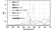
- FIG. 1 is an infrared absorption spectrum obtained using the KBr tablet method of Fourier transform infrared spectroscopy.
- FIG. 2 shows the X-ray diffraction pattern of calcined talc.
- FIG. 3 shows the X-ray diffraction pattern of finely divided talc.
- present embodiment provides a detailed description of the form for carrying out the present invention (hereinafter referred to as the "present embodiment").
- present embodiment is an example for explaining the present invention, and is not intended to limit the present invention to the following content.
- present invention can be carried out with appropriate modifications within the scope of its gist.
- resin solids or “resin solids in a resin composition” refers to the resin components in the resin composition excluding the dielectric powder (A), inorganic filler (B), other fillers, additives (silane coupling agents, wetting and dispersing agents, curing accelerators, and other components), and solvents.
- “100 parts by mass of resin solids” or “total 100 parts by mass of resin solids in a resin composition” refers to the total of 100 parts by mass of resin components in a resin composition excluding the dielectric powder (A), inorganic filler (B), other fillers, additives (silane coupling agents, wetting and dispersing agents, curing accelerators, and other components), and solvents.
- the resin composition of the present embodiment includes a dielectric powder (A) (hereinafter also simply referred to as “dielectric powder (A)”) having a relative dielectric constant of 12.0 or more at a frequency of 10 GHz measured according to a cavity resonator perturbation method, an inorganic filler (B) (hereinafter also simply referred to as “inorganic filler (B)”) different from the dielectric powder (A) and having an absorbance of 0.70 or more at a wavelength of 9.3 ⁇ m and a melting point of 1600° C. or less in an infrared absorption spectrum obtained using Fourier transform infrared spectroscopy, and a thermosetting resin (C).
- A dielectric powder
- inorganic filler (B) inorganic filler
- the resin composition of this embodiment it is possible to suitably manufacture cured products, prepregs, resin sheets, laminates, metal foil-clad laminates, and printed wiring boards that have a high dielectric constant and a low dielectric tangent, excellent thermal properties such as moisture absorption and heat resistance, excellent laser processability, and high metal foil peel strength.
- the resin composition of this embodiment is suitably used for manufacturing insulating layers for printed wiring boards.
- the inventors have discovered that by using a resin composition containing a specific dielectric powder (A), a specific inorganic filler (B), and a thermosetting resin (C) in the insulating layer of a printed wiring board, the substrate on which the insulating layer is laminated is less likely to have the wall surface of the hole gouged out when holes are drilled by laser processing. Therefore, according to this embodiment, it is possible to obtain a cured product that has a high dielectric constant and low dielectric tangent, excellent thermal properties such as moisture absorption and heat resistance, and high metal foil peel strength, while also being excellent due to its laser processability. The reason for this is unclear, but the inventors speculate as follows.
- holes are usually made using a carbon dioxide (CO 2 ) laser, a mechanical drill, an ultraviolet laser (UV laser), and a YAG laser, but a carbon dioxide laser is preferably used because it can accurately process small diameter holes and is excellent in processing speed and cost.
- CO 2 carbon dioxide
- UV laser ultraviolet laser
- YAG laser YAG laser
- a carbon dioxide laser is preferably used because it can accurately process small diameter holes and is excellent in processing speed and cost.
- a carbon dioxide laser is used to make holes, if the insulating layer is formed from a resin composition containing an inorganic filler (B) with a relatively high melting point, the insulating layer tends to be difficult to drill holes with the heat of the carbon dioxide laser.
- the insulating layer can preferably have the high dielectric constant and low dielectric tangent exhibited by the dielectric powder (A).
- the resin layer is able to have excellent thermal properties such as moisture absorption and heat resistance, as well as high metal foil peel strength.
- the inventors therefore presume that, according to this embodiment, it is possible to obtain a cured product or the like that has a high dielectric constant, a low dielectric tangent, excellent thermal properties such as moisture absorption and heat resistance, and high metal foil peel strength, while also having excellent laser processability.
- the reasons are not limited to this.
- the dielectric constant of the dielectric powder (A) is a value at a frequency of 10 GHz measured by the cavity resonator perturbation method.
- the dielectric constant of the dielectric powder (A) can be calculated using the Bruggeman formula (rule of mixtures).
- the dielectric constant can be measured, for example, as follows. That is, the dielectric powder (A) is packed into a PTFE (polytetrafluoroethylene) tube (inner diameter: 1.5 mm), and the dielectric constant of the dielectric powder (A) at a frequency of 10 GHz is measured using a network analyzer. Similarly, the dielectric constant of the PTFE tube at a frequency of 10 GHz is measured using a network analyzer.
- the dielectric constant of the dielectric powder (A) can be calculated from these measured values using the Bruggeman formula (rule of mixtures).
- the measurement of the dielectric constant is performed in an environment of a temperature of 23°C ⁇ 1°C and a humidity of 50% RH (relative humidity) ⁇ 5% RH.
- the specific method of measuring the dielectric constant is as described in the examples.
- the dielectric constant of the dielectric powder (A) is preferably 13.0 or more, and more preferably 15.0 or more. When the dielectric constant is 13.0 or more, an insulating layer having a higher dielectric constant tends to be obtained.
- the upper limit of the dielectric constant is not particularly limited, but is, for example, 100.0 or less.
- the upper limit of the dielectric constant may be 90.0 or less, 80.0 or less, 70.0 or less, 60.0 or less, 50.0 or less, 40.0 or less, or 30.0 or less.
- the dielectric dissipation factor (Df) of the dielectric powder (A) at a frequency of 10 GHz measured according to the cavity resonator perturbation method is preferably 0.015 or less, more preferably 0.010 or less, and even more preferably 0.008 or less. If the dielectric dissipation factor is 0.015 or less, an insulating layer having a lower dielectric dissipation factor tends to be obtained.
- the lower limit of the dielectric dissipation factor is not particularly limited, but is, for example, 0.001 or more.
- the dielectric loss tangent of the dielectric powder (A) can be measured and calculated in the same manner as the relative dielectric constant of the dielectric powder (A) described above.
- the specific method for measuring the dielectric loss tangent is as described in the Examples.
- the average particle diameter (D50) of the dielectric powder (A) is preferably 0.10 ⁇ m or more and 10.00 ⁇ m or less, more preferably 0.15 ⁇ m or more and 8.00 ⁇ m or less, and even more preferably 0.20 ⁇ m or more and 7.50 ⁇ m or less, in order to obtain better dispersibility.
- the average particle diameter (D50) means the value when the particle size distribution of a powder put into a dispersion medium in a predetermined amount is measured using a laser diffraction/scattering type particle size distribution measuring device, and the volume is accumulated from the smallest particles to reach 50% of the total volume.
- the average particle diameter (D50) can be calculated by measuring the particle size distribution using the laser diffraction/scattering method, and the specific measurement method is as described in the examples.
- the absorbance at a wavelength of 9.3 ⁇ m is preferably 0.70 or less, more preferably 0.60 or less, and even more preferably 0.50 or less.
- the lower limit of the absorbance is not particularly limited, but is 0.00 or more.
- the specific method for measuring the absorbance is as described in the Examples.
- the shape of the dielectric powder (A) is not particularly limited, and examples include flake-like, spherical, plate-like, and amorphous shapes.
- the shape is preferably spherical, since this tends to result in a resin composition that disperses better with the thermosetting resin (C), has a higher dielectric constant and a lower dielectric tangent, and has better thermal properties such as moisture absorption and heat resistance, better laser processability, and higher metal foil peel strength, and is suitable for use in the manufacture of insulating layers for printed wiring boards.
- the dielectric powder (A) preferably contains a titanium-based inorganic filler.
- the titanium-based inorganic filler preferably contains at least one selected from the group consisting of surface-uncoated titanium-based inorganic fillers and surface-coated titanium-based inorganic fillers.
- the dielectric powder (A) tends to provide a resin composition having a higher dielectric constant and a lower dielectric loss tangent, better thermal properties such as moisture absorption heat resistance, better laser processability, and higher metal foil peel strength, which is suitable for use in the manufacture of insulating layers for printed wiring boards.
- the surface-uncoated titanium-based inorganic filler more preferably contains at least one selected from the group consisting of titanium monoxide (TiO), titanium dioxide ( TiO2 ), titanium trioxide ( Ti2O3 ), potassium titanate (e.g., K2Ti4O9 ), calcium titanate (e.g., CaTiO3 ), strontium titanate (e.g., SrTiO3 ), barium titanate (e.g., BaTiO3 and BaTi4O9 ), aluminum titanate (e.g., Al2O3.TiO2 ), and lead titanate ( e.g. , PbTiO3 ).
- TiO titanium monoxide
- TiO2 titanium dioxide
- Ti2O3 titanium trioxide
- potassium titanate e.g., K2Ti4O9
- calcium titanate e.g., CaTiO3
- strontium titanate e.g., SrTiO3
- the dielectric powder (A) contains these dielectric powders, there is a tendency for a resin composition or the like that can be obtained that has a higher dielectric constant and a lower dielectric tangent, and has better thermal properties such as moisture absorption and heat resistance, better laser processability, and higher metal foil peel strength, and is suitable for use in producing an insulating layer for a printed wiring board.
- the surface-uncoated titanium-based inorganic filler more preferably contains at least one selected from the group consisting of calcium titanate, strontium titanate, and barium titanate, and even more preferably contains strontium titanate.
- the dielectric powder (A) contains these dielectric powders, it tends to produce a resin composition suitable for use in the manufacture of insulating layers for printed wiring boards, which has a higher dielectric constant and a lower dielectric tangent, better thermal properties such as moisture absorption and heat resistance, better laser processability, and higher metal foil peel strength.
- the dielectric powder (A) contains strontium titanate, in addition to the above effects, it tends to have lower catalytic activity against the thermosetting resin (C) and better moldability.
- strontium titanate a known one can be used, for example, an oxide having a perovskite structure mainly represented by ABO3 can be mentioned.
- Strontium titanate may contain a compound having a structure represented by (SrO) x.TiO2 (0.9 ⁇ x ⁇ 1.0, 1.0 ⁇ x ⁇ 1.1).
- a part of Sr may be replaced with another metal element, for example, at least one of La (lanthanum), Ba (barium), and Ca (calcium).
- a part of Ti may be replaced with another metal element, for example, Zr (zirconium).
- barium titanate a known one can be used, for example, an oxide having a perovskite structure mainly represented by ABO3 .
- Barium titanate may contain a compound having a structure represented by Ba m TiO 2+m (0.995 ⁇ m ⁇ 1.010, 0.995 ⁇ Ba/Ti (molar ratio) ⁇ 1.010).
- Another example of barium titanate is a compound having a structure represented by BaTi 4 O 9.
- a part of Ba may be substituted with another metal element, and such a metal element may be at least one of La (lanthanum), Sr (strontium), and Ca (calcium).
- a part of Ti may be substituted with another metal element, and such a metal element may be Zr (zirconium).
- Calcium titanate may contain a compound having a structure represented by Ca m TiO 2+m (0.995 ⁇ m ⁇ 1.010, 0.995 ⁇ Ca/Ti (molar ratio) ⁇ 1.010).
- a part of Ca may be replaced with another metal element, and such a metal element may be at least one of La (lanthanum), Sr (strontium), and Ca (calcium).
- a part of Ti may be replaced with another metal element, and such a metal element may be Zr (zirconium).
- Titanium dioxide having a rutile or anatase crystal structure is preferred, with rutile crystal structure being more preferred.
- commercially available products can be used as the surface-uncoated titanium-based inorganic filler.
- Commercially available products include, for example, titanium dioxide such as STT-30A and EC-300 manufactured by Titan Kogyo Co., Ltd., AEROXIDE (registered trademark, hereinafter the same) TiO 2 T805 and AEROXIDE TiO 2 NKT90 (all trade names) manufactured by Nippon Aerosil Co., Ltd.; barium titanate such as BT-149 (trade name) manufactured by Nippon Chemical Industry Co., Ltd. and 208108 (all trade names) manufactured by ALDRICH Co., Ltd.; calcium titanate such as CT series manufactured by Fuji Titan Kogyo Co., Ltd.
- titanium dioxide examples include 396141 manufactured by LDRICH Corporation, ST, HST-1, HPST-1, and HPST-2 manufactured by Fuji Titanium Industry Co., Ltd., and SW-100, SW-50C, SW-100C, SW-200C, SW-320C, and SW-350 (all trade names) manufactured by Titanium Industry Co., Ltd.; and titanium trioxide includes STR-100A-LP manufactured by Sakai Chemical Industry Co., Ltd. and MT-N1 (all trade names) manufactured by Teika Co., Ltd.
- the surface-coated titanium-based inorganic filler preferably has an organic layer and/or an inorganic oxide layer on the surface of the titanium-based inorganic filler that is the core of the surface-coated titanium-based inorganic filler.
- the surface-coated titanium-based inorganic filler may be used alone or in combination of two or more types of surface-coated titanium-based inorganic fillers with different particle sizes or surface conditions.
- the core titanium-based inorganic filler can be the above-mentioned uncoated titanium-based inorganic filler.
- organic layer and inorganic oxide layer please refer to the organic layer and inorganic oxide layer described in the section on surface-coated titanium oxide below.
- the average particle diameter (D50) of the titanium-based inorganic filler that serves as the core is preferably 0.10 ⁇ m or more and 10.00 ⁇ m or less, more preferably 0.15 ⁇ m or more and 8.00 ⁇ m or less, and even more preferably 0.20 ⁇ m or more and 7.50 ⁇ m or less, from the viewpoint of dispersibility.
- the average particle diameter (D50) of the titanium-based inorganic filler is determined from the average particle diameter of the primary particles of a single particle.
- the surface-coated titanium-based inorganic filler preferably contains surface-coated titanium oxide.
- the surface-coated titanium oxide preferably has an organic layer and/or an inorganic oxide layer on the surface of a titanium oxide particle (hereinafter simply referred to as a "titanium oxide particle” or "core particle") that serves as the core of the surface-coated titanium oxide.
- a titanium oxide particle hereinafter simply referred to as a "titanium oxide particle” or "core particle”
- One type of surface-coated titanium oxide may be used alone, or two or more types of surface-coated titanium oxides having different particle sizes or surface conditions may be used in combination.
- the total amount (coating amount) of the organic layer and inorganic oxide layer in the surface-coated titanium oxide is preferably 0.1% by mass or more and 10.0% by mass or less, more preferably 1.0% by mass or more and 8.0% by mass or less, and even more preferably 1.0% by mass or more and 4.0% by mass or less, based on 100% by mass of the surface-coated titanium oxide.
- the coating amount is within the above range, a resin composition that is suitable for use in the manufacture of insulating layers for printed wiring boards tends to be obtained, which has a higher dielectric constant and a lower dielectric tangent, better thermal properties such as moisture absorption and heat resistance, better laser processability, and higher metal foil peel strength.
- the content of titanium oxide in the surface-coated titanium oxide is preferably 90.0% by mass or more and 99.9% by mass or less, more preferably 92.0% by mass or more and 99.0% by mass or less, and even more preferably 96.0% by mass or more and 99.0% by mass or less, based on 100% by mass of the surface-coated titanium oxide.
- the content is within the above range, it tends to result in a resin composition that has a higher dielectric constant and a lower dielectric tangent, and has better thermal properties such as moisture absorption and heat resistance, better laser processability, and higher metal foil peel strength, and is suitable for use in the manufacture of insulating layers for printed wiring boards.
- the core particles include titanium monoxide (TiO), titanium trioxide ( Ti2O3 ), and titanium dioxide ( TiO2 ).
- TiO titanium dioxide
- titanium dioxide is preferred. Titanium dioxide having a rutile or anatase crystal structure is preferred, and titanium dioxide having a rutile crystal structure is more preferred.
- the average particle diameter (D50) of the core particles is preferably 0.10 ⁇ m or more and 0.45 ⁇ m or less, and more preferably 0.15 ⁇ m or more and 0.25 ⁇ m or less.
- the average particle diameter (D50) of the core particles is determined from the average particle diameter of the primary particles of a single particle.
- Surface-coated titanium oxide is usually obtained by coating the surface of a core particle with an organic layer or an inorganic oxide layer using a surface treatment agent.
- the surface of the organic layer or inorganic oxide layer coated on the surface of the core particle may be further coated with an organic layer and/or an inorganic oxide layer using a surface treatment agent. Since there is a tendency to obtain resin compositions suitable for use in the manufacture of insulating layers for printed wiring boards, which have a higher dielectric constant and a lower dielectric tangent, better thermal properties such as moisture absorption heat resistance, better laser processability, and higher metal foil peel strength, it is preferable that the surface-coated titanium oxide further has an organic layer on the surface of the inorganic oxide layer coated on the surface of the core particle.
- Coating methods include inorganic treatment and organic treatment. One type of surface treatment agent may be used alone, or two or more types may be used in combination.
- Surface treatment agents used in inorganic treatment include, for example, oxoacids (e.g., silicic acid and aluminic acid), metal salts of oxoacids (e.g., sodium silicate and sodium aluminate), oxides, hydroxides, and hydrated oxides of metals such as aluminum, silicon, zirconium, tin, titanium, antimony, zinc, cobalt, and manganese.
- the surface-coated titanium oxide obtained by inorganic treatment has an inorganic oxide layer on the surface of the titanium oxide particles, the surface of the inorganic oxide layer, or the surface of the organic layer described below.
- Surface treatment agents used in the organic treatment include, for example, organosilicon compounds such as organosilanes, silane coupling agents, and organopolysiloxanes; organotitanium compounds such as titanium coupling agents; and organic substances such as organic acids, polyols, and alkanolamines.
- organosilicon compounds such as organosilanes, silane coupling agents, and organopolysiloxanes
- organotitanium compounds such as titanium coupling agents
- organic substances such as organic acids, polyols, and alkanolamines.
- organosilanes include alkoxysilanes such as n-propyltrimethoxysilane, n-propyltriethoxysilane, hexyltrimethoxysilane, hexyltriethoxysilane, octyltrimethoxysilane, decyltrimethoxysilane, 3-chloropropyltriethoxysilane, phenyltriethoxysilane, and trifluoropropyltrimethoxysilane.
- alkoxysilanes such as n-propyltrimethoxysilane, n-propyltriethoxysilane, hexyltrimethoxysilane, hexyltriethoxysilane, octyltrimethoxysilane, decyltrimethoxysilane, 3-chloropropyltriethoxysilane, phenyltriethoxys
- Silane coupling agents include, for example, aminosilanes such as 3-aminopropyltriethoxysilane, N-2-(aminoethyl)-3-aminopropyltriethoxysilane, and N-phenyl-3-aminopropyltrimethoxysilane; epoxysilanes such as 3-glycidoxypropyltrimethoxysilane and 2-(3,4-epoxycyclohexyl)ethyltrimethoxysilane; methacrylsilanes such as 3-(methacryloyloxypropyl)trimethoxysilane; vinylsilanes such as vinyltrimethoxysilane, vinyltriethoxysilane, and vinyltrichlorosilane; and mercaptosilanes such as 3-mercaptopropyltrimethoxysilane.
- aminosilanes such as 3-aminopropyltriethoxysilane, N-2-(amino
- silicone oil is preferred because it is capable of forming a more uniform organic layer.
- examples of silicone oil include alkyl silicone, alkyl hydrogen silicone, alkoxy silicone, and modified silicone.
- An example of the alkyl silicone is dimethyl silicone.
- Alkyl hydrogen silicones include, for example, methyl hydrogen silicones and ethyl hydrogen silicones.
- the silicone compound containing the alkoxysilyl group in which the alkoxy group is directly or via the divalent hydrocarbon group bonded to the silicon atom is preferred.
- silicone compound for example, linear, cyclic, network, and partially branched linear organopolysiloxane are included.
- linear organopolysiloxane is preferred, and organopolysiloxane having a molecular structure in which the alkoxy group is directly bonded to the silicone main chain is more preferred.
- the alkoxy silicone for example, methoxy silicone and ethoxy silicone are included.
- modified silicones include amino-modified silicones, epoxy-modified silicones, and mercapto-modified silicones.
- Titanium coupling agents include, for example, isopropyl triisostearoyl titanate, isopropyl dimethacryl isostearoyl titanate, and isopropyl tridodecylbenzenesulfonyl titanate.
- organic acids examples include adipic acid, terephthalic acid, lauric acid, myristic acid, palmitic acid, stearic acid, polyhydroxystearic acid, oleic acid, salicylic acid, malic acid, and maleic acid, as well as metal salts thereof.
- polyols examples include trimethylolethane, trimethylolpropane, ditrimethylolpropane, trimethylolpropane ethoxylate, and pentaerythritol.
- alkanolamines include monoethanolamine, monopropanolamine, diethanolamine, dipropanolamine, triethanolamine, and tripropanolamine.
- the surface-coated titanium oxide preferably has an inorganic oxide layer on the surface of the titanium oxide particles, the inorganic oxide layer being one or more selected from the group consisting of a layer containing silica, a layer containing zirconia, and a layer containing alumina, and more preferably the inorganic oxide layer being one or more selected from the group consisting of a layer containing silica and a layer containing alumina.
- thermosetting resin C
- thermosetting resin C
- thermal properties such as moisture absorption and heat resistance, better laser processability, and higher metal foil peel strength, and is suitable for use in the manufacture of insulating layers for printed wiring boards.
- the surface-coated titanium oxide may have two or more inorganic oxide layers.
- the inorganic oxide layer located closer to the titanium oxide particles can further suppress the water absorption by the titanium oxide particles, which are the core particles, and the inorganic oxide layer located farther from the titanium oxide particles can further improve the adhesion to the resin component, the aggregation relaxation of the surface-coated titanium oxide in the resin composition, and the dispersibility.
- the inorganic oxide layer located closer to the core particle is one or more selected from the group consisting of a layer containing silica and a layer containing zirconia, and the inorganic oxide layer located farther from the core particle is a layer containing alumina, and it is more preferable that the inorganic oxide layer located closer to the core particle is a layer containing silica, and the inorganic oxide layer located farther from the core particle is a layer containing alumina.
- the content of the inorganic oxide layer is preferably 0.1% by mass or more and 10.0% by mass or less in total, more preferably 0.3% by mass or more and 7.5% by mass or less, even more preferably 0.4% by mass or more and 5.0% by mass or less, even more preferably 0.5% by mass or more and 4.0% by mass or less, and even more preferably 0.5% by mass or more and 3.3% by mass or less, based on 100% by mass of the surface-coated titanium oxide.
- the coating layer of the surface-coated titanium oxide may have a two-layer structure of an inorganic oxide layer and an organic layer.
- the catalytic activity e.g., photocatalytic activity and metal catalytic activity
- the inorganic oxide layer is preferably one or more selected from the group consisting of a layer containing silica, a layer containing zirconia, and a layer containing alumina, and is more preferably a layer containing alumina because it can further suppress the catalytic activity of titanium oxide while further increasing the affinity with resin.
- the absorbance of the inorganic filler (B) is a value at a wavelength of 9.3 ⁇ m (wave number: 1075 cm ⁇ 1 ) in an infrared absorption spectrum obtained using the KBr tablet method of Fourier transform infrared spectroscopy. A specific method for measuring the absorbance is as described in the Examples.
- the alkaline earth metal silicate preferably includes an alkaline earth metal silicate having the structure Mg 2 Si 2 O 6.
- the alkaline earth metal silicate having the structure Mg 2 Si 2 O 6 is included in, for example, Enstatite and Clinoenstatite.
- Calcined talc can usually be obtained by calcining raw talc, for example, by heat treating the raw talc at a temperature of 900°C or higher and 1500°C or lower for 4 hours or higher and 10 hours or lower.
- raw talc include hydrous magnesium silicate such as a compound having the structure Mg 3 Si 4 O 10 (OH) 2.
- the shape of raw talc include fine powder and powder. When the raw talc is in the form of powder, its average particle size (D50) is usually about 1.0 ⁇ m or higher and 7.0 ⁇ m or lower.
- Calcined talc is an alkaline earth metal silicate having the structure Mg 2 Si 2 O 6 .
- the content of the inorganic filler (B) is preferably 10 parts by mass or more and 200 parts by mass or less, more preferably 15 parts by mass or more and 150 parts by mass or less, even more preferably 20 parts by mass or more and 125 parts by mass or less, even more preferably 40 parts by mass or more and 110 parts by mass or less, and even more preferably 30 parts by mass or more and 100 parts by mass or less, relative to 100 parts by mass of the total resin solid content in the resin composition.
- thermosetting resin (C) The resin composition of the present embodiment contains a thermosetting resin (C).
- the thermosetting resin (C) is not particularly limited as long as it is a thermosetting resin or compound.
- the thermosetting resin (C) may be used alone or in combination of two or more kinds.
- maleimide compound a maleimide compound having an aromatic skeleton is preferable.
- maleimide compounds include N-phenylmaleimide, N-hydroxyphenylmaleimide, bis(4-maleimidophenyl)methane, 2,2-bis(4-(4-maleimidophenoxy)-phenyl)propane, bis(3,5-dimethyl-4-maleimidophenyl)methane, bis(3-ethyl-5-methyl-4-maleimidophenyl)methane, bis(3,5-diethyl-4-maleimidophenyl)methane, maleimide compounds represented by the following formula (1), maleimide compounds represented by the following formula (2), maleimide compounds represented by the following formula (3), and maleimide compounds represented by the following formula (4), prepolymers of these maleimide compounds, and prepolymers of the above maleimide compounds and amine compounds.
- thermosetting resin (C) contains the maleimide compound, it tends to produce a resin composition that has a higher dielectric constant and a lower dielectric tangent, and has better thermal properties such as moisture absorption and heat resistance, better laser processability, and higher metal foil peel strength, and is suitable for use in the manufacture of insulating layers for printed wiring boards.
- the maleimide compound contains a maleimide compound represented by the following formula (2).
- the thermosetting resin (C) contains a maleimide compound represented by formula (2), it tends to produce a resin composition that is suitable for use in the manufacture of insulating layers for printed wiring boards, which has a higher dielectric constant than the first layer, in particular a lower dielectric tangent than the first layer, and has better thermal properties such as better moisture absorption and heat resistance, as well as better laser processability and higher metal foil peel strength.
- each R 1 independently represents a hydrogen atom or a methyl group, and n1 represents an integer of 1 to 10.
- each Ra independently represents an alkyl group, alkyloxy group, or alkylthio group having 1 to 10 carbon atoms, an aryl group, aryloxy group, or arylthio group having 6 to 10 carbon atoms, a cycloalkyl group having 3 to 10 carbon atoms, a halogen atom, a nitro group, a hydroxy group, or a mercapto group.
- q represents an integer from 0 to 4. When q is an integer from 2 to 4, Ra may be the same or different within the same ring.
- Each Rb independently represents an alkyl group, alkyloxy group, or alkylthio group having 1 to 10 carbon atoms, an aryl group, aryloxy group, or arylthio group having 6 to 10 carbon atoms, a cycloalkyl group having 3 to 10 carbon atoms, a halogen atom, a hydroxy group, or a mercapto group.
- r represents an integer from 0 to 3. When r is 2 or 3, Rb may be the same or different within the same ring.
- n3 is an average value and represents a value of 0.95 to 10.0.
- alkyl groups having 1 to 10 carbon atoms include the alkyl groups having 1 to 5 carbon atoms listed above, as well as n-pentyl, isopentyl, neopentyl, n-hexyl, isohexyl, n-heptyl, n-octyl, 2-ethylhexyl, n-nonyl, isononyl, and n-decyl groups.
- alkyloxy groups having 1 to 10 carbon atoms examples include methoxy groups, ethoxy groups, n-propoxy groups, n-butoxy groups, n-pentyloxy groups, and n-hexyloxy groups.
- alkylthio groups having 1 to 10 carbon atoms examples include methylthio and ethylthio groups.
- aryl groups having 6 to 10 carbon atoms include phenyl groups, cyclohexylphenyl groups, phenol groups, cyanophenyl groups, nitrophenyl groups, naphthalene groups, biphenyl groups, anthracene groups, naphthacene groups, anthracyl groups, pyrenyl groups, perylene groups, pentacene groups, benzopyrene groups, chrysene groups, pyrene groups, and triphenylene groups.
- arylthio groups having 6 to 10 carbon atoms include phenylthio and p-tolylthio groups.
- cycloalkyl groups having 3 to 10 carbon atoms include cyclopropyl, cyclobutyl, cyclopentyl, cyclohexyl, and cycloheptyl groups.
- Halogen atoms include, for example, fluorine atoms, chlorine atoms, bromine atoms, and iodine atoms.
- each Ra is preferably independently an alkyl group having 1 to 6 carbon atoms, a cycloalkyl group having 3 to 6 carbon atoms, or an aryl group having 6 to 10 carbon atoms.
- r is preferably 0. It is also preferable that r is an integer from 1 to 3, and each Rb is independently an alkyl group having 1 to 6 carbon atoms, a cycloalkyl group having 3 to 6 carbon atoms, or an aryl group having 6 to 10 carbon atoms.
- the groups other than Rb that are directly bonded to the benzene ring are hydrogen atoms.
- the maleimide compound represented by formula (3) may be produced according to a known method. Specific examples of the production method include the method described in WO2020/217679.
- v is preferably an integer from 0 to 3.
- R4 represents a hydrogen atom or a group represented by formula (5).
- Formula (5) is as defined above.
- R 5 represents a hydrogen atom or a group represented by formula (6).
- the alkyl group having 1 to 10 carbon atoms in R7 is the same as the alkyl group having 1 to 10 carbon atoms in R1 , including preferred embodiments.
- w in formula (6) is the same as s in formula (4), including preferred embodiments.
- R 8 each independently represents a group represented by formula (5).
- the group represented by formula (5) is as described above.
- x is the same as u in formula (4), including preferred embodiments.
- *2 indicates the bonding site to the carbon atom in the -CH(CH 3 )- group.
- n4 preferably represents an integer from 1 to 90, and more preferably represents an integer from 1 to 80.
- the weight average molecular weight (Mw) of the maleimide compound represented by formula (4) is preferably 400 or more and 500,000 or less, more preferably 450 or more and 400,000 or less.
- the number average molecular weight (Mn) of the maleimide compound represented by formula (4) is preferably 350 or more and 2,000 or less, more preferably 400 or more and 1,500 or less.
- the molecular weight distribution (Mw/Mn) of the maleimide compound represented by formula (4) is preferably 1.001 or more and 500 or less, more preferably 1.001 or more and 400 or less.
- Mw, Mn, and Mw/Mn can be determined by gel permeation chromatography (GPC) using polystyrene standard equivalents.
- the maleimide compound represented by formula (4) may be produced according to a known method.
- a specific production method is, for example, the method described in JP-A-2023-7239.
- the maleimide compound may be a commercially available product, or a product produced by a known method.
- Commercially available maleimide compounds include, for example, BMI-70 (bis(3-ethyl-5-methyl-4-maleimidophenyl)methane), BMI-80 (2,2-bis(4-(4-maleimidophenoxy)-phenyl)propane), and BMI-1000P (all trade names, manufactured by K.I.
- BMI-3000, BMI-4000, BMI-5100, BMI-7000, and BMI-2300 maleimide compounds represented by the above formula (1)
- MIR-3000-70MT trade name, manufactured by Daiwa Kasei Co., Ltd.
- the content of the maleimide compound is preferably 15 parts by mass or more and 85 parts by mass or less, more preferably 20 parts by mass or more and 80 parts by mass or less, and even more preferably 25 parts by mass or more and 75 parts by mass or less, relative to 100 parts by mass of the total resin solid content in the resin composition.
- the content of the maleimide compound is within the above range, it tends to be possible to obtain a resin composition that is suitable for use in the manufacture of insulating layers for printed wiring boards, having a higher dielectric constant and a lower dielectric tangent, better thermal properties such as moisture absorption and heat resistance, better laser processability, and higher metal foil peel strength.
- the resin composition contains two or more types of maleimide compounds, it is preferable that the total amount thereof is within the above range.
- cyanate ester compounds examples include aryloxy compounds, biphenyl aralkyl cyanate ester compounds, bis(3,3-dimethyl-4-cyanatophenyl)methane, 1,3-dicyanatobenzene, 1,4-dicyanatobenzene, 1,3,5-tricyanatobenzene, 1,3-dicyanatonaphthalene, 1,4-dicyanatonaphthalene, 1,6-dicyanatonaphthalene, 1,8-dicyanatonaphthalene, 2,6-dicyanatonaphthalene, 2,7-dicyanatonaphthalene, 1,3,6-tricyanatonaphthalene, 4,4'-dicyanatobiphenyl, bis(4-cyanatophenyl)ether, bis(4-cyanatophenyl)thioether, and bis(4-cyanatophenyl)sulfone. These cyanate ester compounds may also be prepolymers or polymers of the cyanate ester compounds.
- the cyanate ester compound preferably includes one or more selected from the group consisting of phenol novolac type cyanate ester compounds, naphthol aralkyl type cyanate ester compounds, naphthylene ether type cyanate ester compounds, xylene resin type cyanate ester compounds, bisphenol M type cyanate ester compounds, bisphenol A type cyanate ester compounds, diallyl bisphenol A type cyanate ester compounds, bisphenol E type cyanate ester compounds, bisphenol F type cyanate ester compounds, and biphenyl aralkyl type cyanate ester compounds, as well as prepolymers or polymers of these cyanate ester compounds, more preferably includes one or more selected from the group consisting of naphthol aralkyl type cyanate ester compounds and bisphenol A type cyanate ester compounds, and even more preferably includes a naphthol aralkyl type cyanate ester compound.
- thermosetting resin (C) contains the above-mentioned cyanate ester compound
- a resin composition to be obtained that has a higher dielectric constant and a lower dielectric tangent, and has better thermal properties such as moisture absorption and heat resistance, better laser processability, and higher metal foil peel strength, and is suitable for use in the manufacture of insulating layers for printed wiring boards.
- R6 each independently represents a hydrogen atom or a methyl group, and among these, a hydrogen atom is preferred.
- n5 represents an integer of 1 or more, preferably an integer of 1 to 20, and more preferably an integer of 1 to 10.
- bisphenol A type cyanate ester compound one or more compounds selected from the group consisting of 2,2-bis(4-cyanatophenyl)propane and prepolymers of 2,2-bis(4-cyanatophenyl)propane may be used.
- a bisphenol A type cyanate ester compound commercially available products may be used, and examples thereof include Primaset (registered trademark) BADCy (trade name, Lonza Co., Ltd., 2,2-bis(4-cyanatophenyl)propane, cyanate ester group equivalent: 139 g/eq.) and CA210 (trade name, Mitsubishi Gas Chemical Co., Ltd., prepolymer of 2,2-bis(4-cyanatophenyl)propane, cyanate ester group equivalent: 139 g/eq.).
- Primaset registered trademark
- BADCy trade name, Lonza Co., Ltd., 2,2-bis(4-cyanatophenyl)propane, cyanate ester group equivalent: 139 g/eq.
- CA210 trade name, Mitsubishi Gas Chemical Co., Ltd., prepolymer of 2,2-bis(4-cyanatophenyl)propane, cyanate ester group equivalent: 139 g/eq.
- cyanate ester compounds may be produced according to known methods. Specific production methods include, for example, those described in JP 2017-195334 A (particularly paragraphs 0052 to 0057).
- the content of the cyanate ester compound is preferably 1 part by mass or more and 65 parts by mass or less, more preferably 2 parts by mass or more and 60 parts by mass or less, even more preferably 3 parts by mass or more and 55 parts by mass or less, even more preferably 4 parts by mass or more and 50 parts by mass or less, even more preferably 5 parts by mass or more and 45 parts by mass or less, and even more preferably 6 parts by mass or more and 40 parts by mass or less, relative to 100 parts by mass of the total resin solid content in the resin composition.
- the content of the cyanate ester compound is within the above range, a resin composition that is suitable for use in the manufacture of insulating layers for printed wiring boards, which has a higher dielectric constant and a lower dielectric tangent, better thermal properties such as moisture absorption and heat resistance, better laser processability, and higher metal foil peel strength, tends to be obtained.
- the resin composition contains two or more types of cyanate ester compounds, it is preferable that the total amount thereof is within the above range.
- the resin composition of the present embodiment preferably contains an epoxy compound.
- the thermosetting resin (C) contains an epoxy compound, there is a tendency for a resin composition or the like that is suitable for use in producing an insulating layer for a printed wiring board to be obtained, which has a higher dielectric constant and a lower dielectric tangent, and has better thermal properties such as moisture absorption and heat resistance, better laser processability, and higher metal foil peel strength.
- the epoxy compound is not particularly limited, and any known compound having one or more epoxy groups in one molecule can be used as appropriate.
- the number of epoxy groups in one molecule of the epoxy compound is one or more, and preferably two or more.
- the epoxy compounds may be used alone or in combination of two or more.
- epoxy compound conventionally known epoxy compounds and epoxy resins can be used.
- biphenyl aralkyl type epoxy resins naphthalene type epoxy resins, bisnaphthalene type epoxy resins, multifunctional phenol type epoxy resins, naphthylene ether type epoxy resins, butadiene skeleton-containing epoxy resins, phenol aralkyl type epoxy resins, phenol novolac type epoxy resins, cresol novolac type epoxy resins, xylene novolac type epoxy resins, naphthalene skeleton-modified novolac type epoxy resins, dicyclopentadiene novolac type epoxy resins, biphenyl novolac type epoxy resins, phenol aralkyl novolac type epoxy resins, naphthol aralkyl novolac type epoxy resins, aralkyl novolac type epoxy resins, aromatic hydrocarbon formaldehyde type epoxy compounds, anthraquinone type epoxy compounds, anthracene
- R represents a hydrogen atom or an alkyl group having 1 to 10 carbon atoms
- a and b each independently represent an integer from 1 to 100
- c and d each independently represent an integer from 0 to 100.
- alkyl group include a methyl group, an ethyl group, a propyl group, and a butyl group.
- e is an integer between 24 and 35, and f is an integer between 8 and 11.
- the butadiene skeleton-containing epoxy resin may be a commercially available product, or a product produced by a known method.
- the content of the epoxy compound is preferably 1 part by mass or more and 50 parts by mass or less, more preferably 10 parts by mass or more and 45 parts by mass or less, and even more preferably 20 parts by mass or more and 40 parts by mass or less, relative to 100 parts by mass of the total resin solid content in the resin composition.
- the content of the epoxy compound is within the above range, it tends to be possible to obtain a resin composition that is suitable for use in the manufacture of insulating layers for printed wiring boards, having a higher dielectric constant and a lower dielectric tangent, better thermal properties such as moisture absorption and heat resistance, better laser processability, and higher metal foil peel strength.
- the resin composition contains two or more types of epoxy compounds, it is preferable that the total amount thereof is within the above range.
- the resin composition of the present embodiment may contain a phenol compound.
- the phenol compound may be any known compound having two or more phenolic hydroxy groups in one molecule, and the type of the phenol compound is not particularly limited.
- the phenol compound may be used alone or in combination of two or more.
- phenolic compounds include cresol novolac type phenolic resins, biphenyl aralkyl type phenolic resins represented by the following formula (15), naphthol aralkyl type phenolic resins represented by the following formula (16), aminotriazine novolac type phenolic resins, naphthalene type phenolic resins, phenol novolac resins, alkylphenol novolac resins, bisphenol A type novolac resins, dicyclopentadiene type phenolic resins, xyloc type phenolic resins, terpene modified phenolic resins, and polyvinyl phenols.
- cresol novolac type phenolic resins one or more selected from the group consisting of cresol novolac type phenolic resins, biphenyl aralkyl type phenolic resins represented by formula (15), naphthol aralkyl type phenolic resins represented by formula (16), aminotriazine novolac type phenolic resins, and naphthalene type phenolic resins are preferred, as they provide excellent moldability and surface hardness, and one or more selected from the group consisting of biphenyl aralkyl type phenolic resins represented by formula (15) and naphthol aralkyl type phenolic resins represented by formula (16) are more preferred.
- each R 4 independently represents a hydrogen atom or a methyl group, and n4 is an integer of 1 to 10.
- each R 5 independently represents a hydrogen atom or a methyl group, and n5 is an integer of 1 to 10.
- the content of the phenolic compound is preferably 1 part by mass or more and 50 parts by mass or less, more preferably 5 parts by mass or more and 40 parts by mass or less, and even more preferably 10 parts by mass or more and 30 parts by mass or less, relative to 100 parts by mass of the total resin solid content of the resin composition.
- the content of the phenolic compound is within the above range, the adhesiveness, flexibility, etc. tend to be superior.
- the resin composition contains two or more types of phenolic compounds, it is preferable that their total amount is within the above range.
- the resin composition of the present embodiment may contain a modified polyphenylene ether compound.
- the modified polyphenylene ether compound may be any known compound as long as the terminals of the polyphenylene ether compound are partially or entirely modified, and is not particularly limited.
- the term "modified" of the modified polyphenylene ether compound means that the terminals of the polyphenylene ether compound are partially or entirely substituted with reactive functional groups. Examples of the reactive functional group include a group having a carbon-carbon unsaturated double bond and a hydroxy group.
- the modified polyphenylene ether compound may be used alone or in combination of two or more.
- the polyphenylene ether compound related to the modified polyphenylene ether compound may be, for example, a polymer containing at least one structural unit selected from the structural unit represented by formula (17), the structural unit represented by formula (18), and the structural unit represented by formula (19).
- R 8 , R 9 , R 10 , and R 11 each independently represent an alkyl group having 6 or less carbon atoms, an aryl group, a halogen atom, or a hydrogen atom.
- R12 , R13 , R14 , R18 , and R19 each independently represent an alkyl group having 6 or less carbon atoms or a phenyl group.
- R15 , R16 , and R17 each independently represent a hydrogen atom, an alkyl group having 6 or less carbon atoms, or a phenyl group.
- R 20 , R 21 , R 22 , R 23 , R 24 , R 25 , R 26 , and R 27 each independently represent a hydrogen atom, an alkyl group having 6 or less carbon atoms, or a phenyl group, and -A- represents a linear, branched, or cyclic divalent hydrocarbon group having 20 or less carbon atoms.
- -A- in formula (19) may be, for example, a divalent organic group such as a methylene group, an ethylidene group, a 1-methylethylidene group, a 1,1-propylidene group, a 1,4-phenylenebis(1-methylethylidene) group, a 1,3-phenylenebis(1-methylethylidene) group, a cyclohexylidene group, a phenylmethylene group, a naphthylmethylene group, or a 1-phenylethylidene group, but is not limited to these.
- a divalent organic group such as a methylene group, an ethylidene group, a 1-methylethylidene group, a 1,1-propylidene group, a 1,4-phenylenebis(1-methylethylidene) group, a 1,3-phenylenebis(1-methylethylidene
- modified polyphenylene ether compounds include those in which all or part of the terminals of the polyphenylene ether compound are modified with functional groups such as ethylenically unsaturated groups such as vinylbenzyl groups, epoxy groups, amino groups, hydroxyl groups, mercapto groups, carboxy groups, methacryloyl groups, and silyl groups.
- functional groups such as ethylenically unsaturated groups such as vinylbenzyl groups, epoxy groups, amino groups, hydroxyl groups, mercapto groups, carboxy groups, methacryloyl groups, and silyl groups.
- modified polyphenylene ether compound having a hydroxyl group at the end is SA90 (trade name, SABIC Innovative Plastics).
- modified polyphenylene ether compound having a methacryloyl group at the end is SA9000 (trade name, SABIC Innovative Plastics).
- the method for producing the modified polyphenylene ether compound is not particularly limited as long as it can obtain the effects of the present invention.
- the compound can be produced by the method described in Japanese Patent No. 4,591,665.
- the modified polyphenylene ether compound more preferably contains a modified polyphenylene ether compound having an ethylenically unsaturated group at its end.
- the ethylenically unsaturated group may include alkenyl groups such as ethenyl, allyl, acryloyl, methacryloyl, propenyl, butenyl, hexenyl, and octenyl; cycloalkenyl groups such as cyclopentenyl and cyclohexenyl; and alkenylaryl groups such as vinylbenzyl and vinylnaphthyl.Among them, vinylbenzyl is preferred.
- the terminal ethylenically unsaturated groups may be single or multiple and may be the same functional group or different functional groups.
- a compound represented by the following formula (20) is preferred.
- X represents an aromatic group
- -(Y-O) m - represents a polyphenylene ether moiety
- R 1 , R 2 , and R 3 each independently represent a hydrogen atom, an alkyl group, an alkenyl group, or an alkynyl group
- m represents an integer of 1 to 100
- n represents an integer of 1 to 6
- q represents an integer of 1 to 4.
- m is preferably an integer of 1 to 50, more preferably an integer of 1 to 30.
- n is preferably an integer of 1 to 4, more preferably 1 or 2, and ideally 1.
- q is preferably an integer of 1 to 3, more preferably 1 or 2, and ideally 2.
- the aromatic group represented by X in formula (20) may be a group in which q hydrogen atoms have been removed from one ring structure selected from a benzene ring structure, a biphenyl ring structure, an indenyl ring structure, and a naphthalene ring structure (e.g., a phenylene group, a biphenylene group, an indenylene group, and a naphthylene group).
- a biphenylene group is preferred.
- the structural unit represented by formula (17), the structural unit represented by formula (18), and the structural unit represented by formula (19) can be used. Among them, it is more preferable to include the structural unit represented by formula (17).
- the number average molecular weight is preferably 500 or more and 7000 or less.
- one having a minimum melt viscosity of 50000 Pa ⁇ s or less can be used.
- the number average molecular weight is preferably 1000 or more and 7000 or less, and the minimum melt viscosity is more preferably 50000 Pa ⁇ s or less.
- the number average molecular weight is measured by gel permeation chromatography according to a standard method.
- the number average molecular weight is preferably 1,000 or more and 3,000 or less.
- the minimum melt viscosity is measured using a dynamic viscoelasticity measuring device according to a standard method.
- the minimum melt viscosity is more preferably 500 Pa ⁇ s or more and 50,000 Pa ⁇ s or less.
- the resin composition of the present embodiment may contain components other than those described above, provided that the intended properties are not impaired.
- the other components include flame retardant compounds such as bromine compounds such as 4,4'-dibromobiphenyl, nitrogen-containing compounds such as melamine and benzoguanamine, and silicon-based compounds.
- flame retardant compounds such as bromine compounds such as 4,4'-dibromobiphenyl
- nitrogen-containing compounds such as melamine and benzoguanamine
- silicon-based compounds examples of various additives include ultraviolet absorbers, antioxidants, photopolymerization initiators, fluorescent brighteners, photosensitizers, dyes, pigments, thickeners, lubricants, defoamers, dispersants, leveling agents (surface conditioners), gloss agents, and polymerization inhibitors.
- the content of the other components is not particularly limited, but is usually 0.01 parts by mass or more and 10 parts by mass or less for each 100 parts by mass of the total resin solids in the resin composition.
- the method for producing the resin composition of this embodiment includes, for example, a method of mixing the dielectric powder (A), the inorganic filler (B), the thermosetting resin (C), and, if necessary, the above-mentioned components, and thoroughly stirring the mixture.
- known treatments such as stirring, mixing, and kneading treatment can be performed.
- the stirring and dispersion treatment using a stirring tank equipped with a stirrer having an appropriate stirring capacity, the dispersibility of the dielectric powder (A), the inorganic filler (B), and other fillers mixed as necessary in the resin composition can be improved.
- the above stirring, mixing, and kneading treatments can be appropriately performed using, for example, a device for mixing such as a ball mill or a bead mill, or a known device such as a revolving or rotating type mixer.
- a solvent can be used as necessary to prepare a resin varnish.
- the resin varnish can be obtained by a known method.
- the resin varnish can be obtained by adding 10 parts by mass or more and 900 parts by mass or less of an organic solvent to 100 parts by mass of the components in the resin composition excluding the organic solvent, and performing the known treatments (stirring, mixing, kneading, etc.) described above.
- the type of solvent as long as it is capable of dissolving the resin in the resin composition. Specific examples are as described above.
- the resin composition of the present embodiment can be suitably used as a raw material for, for example, a cured product, a prepreg, a film-like underfill material, a resin sheet, a laminate, a build-up material, a non-conductive film, a metal foil-clad laminate, a printed wiring board, and a fiber-reinforced composite material, or in the manufacture of a semiconductor device.
- the resin composition is suitably used for a printed wiring board. These will be described below.
- the prepreg of this embodiment includes a substrate and the resin composition of this embodiment impregnated or applied to the substrate.
- the prepreg can be obtained, for example, by impregnating or applying the resin composition (for example, uncured state (A stage)) to the substrate, and then semi-curing (B stage) by a method of heating and drying at 120 ° C. to 220 ° C. for about 2 minutes to 15 minutes.
- the amount of the resin composition (including the cured product of the resin composition) attached to the substrate is preferably in the range of 20% by mass to 99% by mass.
- the semi-cured state (B stage) refers to a state in which each component contained in the resin composition has not actively started to react (cure), but the resin composition is in a dry state, that is, the resin composition is heated to a degree that is not sticky, and the solvent is evaporated. It also includes a state in which the solvent is only evaporated without curing even without heating.
- the substrate is not particularly limited as long as it is a substrate used in various printed wiring board materials.
- the substrate material include glass fiber (e.g., E-glass, D-glass, L-glass, S-glass, T-glass, Q-glass, UN-glass, and NE-glass, etc.), inorganic fibers other than glass fiber (e.g., quartz, etc.), and organic fibers (e.g., polyimide, polyamide, polyester, liquid crystal polyester, and polytetrafluoroethylene, etc.).
- the form of the substrate is not particularly limited, and examples include woven fabric, nonwoven fabric, roving, chopped strand mat, and surfacing mat. These substrates may be used alone or in combination of two or more.
- woven fabric that has been subjected to ultra-opening treatment and clogging treatment is preferred, and glass woven fabric that has been surface-treated with a silane coupling agent such as epoxy silane treatment and amino silane treatment is preferred from the viewpoint of obtaining better processability and thermal properties such as moisture absorption and heat resistance.
- a silane coupling agent such as epoxy silane treatment and amino silane treatment
- Glass fibers such as E-glass, L-glass, NE-glass, and Q-glass are preferred because they provide better processability and dielectric properties.
- the resin sheet of the present embodiment includes the resin composition of the present embodiment.
- the resin sheet may be a resin sheet with a support, which includes a support and a layer formed from the resin composition of the present embodiment arranged on the surface of the support.
- the resin sheet can be used as a build-up film or a dry film solder resist.
- the method for producing the resin sheet is not particularly limited, but for example, a method of obtaining a resin sheet by applying (coating) a solution in which the resin composition is dissolved in a solvent to a support and drying the solution can be mentioned.
- the support examples include, but are not limited to, polyethylene film, polypropylene film, polycarbonate film, polyethylene terephthalate film, ethylene tetrafluoroethylene copolymer film, and release films obtained by applying a release agent to the surface of these films, organic film substrates such as polyimide film, metal foils such as copper foil and aluminum foil, glass plates, SUS plates, FRP, and other plate-shaped substrates.
- Examples of application methods include a method in which a solution of the resin composition dissolved in a solvent is applied onto a support using a bar coater, die coater, doctor blade, baker applicator, or the like.
- a single-layer sheet can be obtained by peeling or etching the support from a resin sheet with a support in which the support and the resin composition are laminated. Note that a single-layer sheet (resin sheet) can also be obtained without using a support by supplying a solution of the resin composition dissolved in a solvent into a mold having a sheet-shaped cavity and drying it to form it into a sheet.
- the drying conditions for removing the solvent are not particularly limited, but from the viewpoint of facilitating removal of the solvent in the resin composition and suppressing the progress of curing during drying, the temperature is preferably in the range of 20°C to 200°C and the drying time is preferably in the range of 1 minute to 90 minutes.
- the resin composition can be used in an uncured state in which the solvent has simply been dried, or it can be used in a semi-cured (B-stage) state as necessary.
- the thickness of the resin layer of the single layer sheet or the resin sheet with a support can be adjusted by the concentration of the solution of the resin composition and the coating thickness, and is not particularly limited, but from the viewpoint of facilitating removal of the solvent during drying, it is preferably in the range of 0.1 ⁇ m to 500 ⁇ m.
- the laminate of this embodiment includes one or more selected from the group consisting of the prepreg and resin sheet of this embodiment.
- the resin compositions used in each prepreg and resin sheet may be the same or different.
- the resin compositions used therein may be the same or different.
- one or more selected from the group consisting of prepregs and resin sheets may be in a semi-cured state (B stage) or a completely cured state (C stage).
- the metal foil-clad laminate of this embodiment includes the laminate of this embodiment and metal foil disposed on one or both sides of the laminate. Furthermore, a metal foil-clad laminate may include at least one prepreg of the present embodiment and metal foil laminated on one or both sides of the prepreg. Furthermore, the metal foil-clad laminate may include at least one resin sheet of the present embodiment and a metal foil laminated on one or both sides of the resin sheet.
- the resin compositions used in each prepreg and resin sheet may be the same or different, and when both a prepreg and a resin sheet are used, the resin compositions used in them may be the same or different.
- one or more selected from the group consisting of prepregs and resin sheets may be in a semi-cured state or in a fully cured state.
- the metal foil is laminated on one or more surfaces selected from the group consisting of prepregs and resin sheets, and it is preferable that the metal foil is laminated so as to be in contact with the surface of one or more surfaces selected from the group consisting of prepregs and resin sheets.
- the metal foil is laminated so as to be in contact with the surface of one or more surfaces selected from the group consisting of prepregs and resin sheets" means that there is no layer such as an adhesive layer between the prepreg or resin sheet and the metal foil, and the prepreg or resin sheet and the metal foil are in direct contact. This increases the metal foil peel strength of the metal foil clad laminate, and tends to improve the insulation reliability of printed wiring boards.
- the metal foil-clad laminate may have one or more overlapping prepregs and/or resin sheets, and metal foils arranged on one or both sides of the prepregs and/or resin sheets.
- Examples of the manufacturing method of the metal foil-clad laminate include a method of stacking one or more prepregs and/or resin sheets, and arranging metal foils on one or both sides of the stack to perform lamination molding.
- Examples of the molding method include methods that are commonly used when molding laminates and multilayer boards for printed wiring boards.
- examples of the method include a method of lamination molding using a multi-stage press machine, a multi-stage vacuum press machine, a continuous molding machine, an autoclave molding machine, etc., at a temperature of about 180°C to about 350°C, a heating time of about 100 minutes to about 300 minutes, and a surface pressure of about 20 kgf/cm2 to about 100 kgf/ cm2 .
- a multilayer board can be produced by combining prepregs and/or resin sheets with a separately prepared wiring board for an inner layer and laminating and molding the prepregs and/or resin sheets.
- a method for producing a multilayer board for example, copper foil having a thickness of about 1.5 ⁇ m to 70 ⁇ m is placed on both sides of one or more stacked prepregs and/or resin sheets, and laminated and formed by the above-mentioned molding method to produce a copper foil-clad laminate, and then an inner layer circuit is formed, and this circuit is blackened to form an inner layer circuit board, and then this inner layer circuit board and prepregs and/or resin sheets are arranged alternately one by one, and copper foil is further arranged as the outermost layer, and laminated and molded under the above-mentioned conditions, preferably under vacuum, to produce a multilayer board.
- Metal foil-clad laminates can be suitably used as printed wiring boards.
- the metal foil is not particularly limited, and examples thereof include gold foil, silver foil, copper foil, tin foil, nickel foil, and aluminum foil. Among these, copper foil is preferred.
- the copper foil is not particularly limited as long as it is generally used as a material for printed wiring boards, and examples thereof include rolled copper foil and electrolytic copper foil. Among these, electrolytic copper foil is preferred from the viewpoint of copper foil peel strength and fine wiring formability.
- the thickness of the copper foil is not particularly limited, and may be about 1.5 ⁇ m or more and 70 ⁇ m or less.
- the roughness Rz of the copper foil surface is adjusted to 0.2 ⁇ m or more and 4.0 ⁇ m or less.
- the roughness Rz of the copper foil surface By having the roughness Rz of the copper foil surface of 0.2 ⁇ m or more, the roughness of the copper foil surface tends to be moderate, and the copper foil peel strength tends to be further improved.
- the roughness Rz of the copper foil surface of 4.0 ⁇ m or less By having the roughness Rz of the copper foil surface of 4.0 ⁇ m or less, the roughness of the copper foil surface tends to be moderate, and the dielectric tangent of the obtained cured product tends to be further improved.
- the roughness Rz is measured in accordance with JIS B0601:2013.
- the lower limit of the roughness Rz of the copper foil surface is more preferably 0.5 ⁇ m or more, even more preferably 0.6 ⁇ m or more, and even more preferably 0.7 ⁇ m or more.
- the upper limit of the roughness Rz of the copper foil surface is more preferably 3.5 ⁇ m or less, even more preferably 3.0 ⁇ m or less, and even more preferably 2.0 ⁇ m or less.
- the printed wiring board of the present embodiment has an insulating layer and a conductor layer disposed on one or both sides of the insulating layer, and the insulating layer contains a cured product of the resin composition of the present embodiment.
- the insulating layer preferably contains at least one of a layer (a layer containing a cured product) formed from a resin composition and a layer (a layer containing a cured product) formed from a prepreg.
- a printed wiring board can be manufactured according to a conventional method, and the manufacturing method is not particularly limited, but can be manufactured, for example, using the above-mentioned metal foil-clad laminate. An example of a method for manufacturing a printed wiring board is shown below.
- the metal foil-clad laminate is prepared.
- the surface of the metal foil-clad laminate is etched to form an inner layer circuit, and an inner layer board is produced. If necessary, the surface of the inner layer circuit of this inner layer board is subjected to a surface treatment (roughening treatment method) to increase the adhesive strength, and then the required number of prepregs described above are stacked on the surface of the inner layer circuit, and metal foil for the outer layer circuit is further laminated on the outside of it, and heated and pressed to form an integral mold.
- a multilayer laminate is produced in which an insulating layer made of a base material and a cured product of a resin composition is formed between the inner layer circuit and the metal foil for the outer layer circuit.
- this multilayer laminate is subjected to a hole drilling process for through holes and via holes.
- a plated metal film that conducts electricity between the inner layer circuit and the metal foil for the outer layer circuit is formed by a metal plating process on the wall surface of the hole, and if necessary, the metal foil for the outer layer circuit is further etched to form the outer layer circuit, thereby producing a printed wiring board.
- the hole drilling process for the through holes and via holes is performed, it is preferable to perform a roughening process including a desmear process.
- the printed wiring board obtained in the above manufacturing example has an insulating layer and a conductor layer formed on the surface of this insulating layer, and the insulating layer contains a cured product of the resin composition.
- the prepreg of this embodiment including a substrate and a cured product of the resin composition of this embodiment impregnated or applied thereto
- the layer of the resin composition of the metal foil-clad laminate of this embodiment (a layer containing a cured product of the resin composition of this embodiment) are composed of an insulating layer containing a cured product of the resin composition of this embodiment.
- the resin composition of this embodiment has a high dielectric constant and a low dielectric tangent, excellent thermal properties such as moisture absorption and heat resistance, and high metal foil peel strength, while also having excellent laser processability. Therefore, by using the resin composition, it is possible to obtain a printed wiring board having an insulating layer with higher insulation reliability, while having a high dielectric constant, a low dielectric tangent, excellent thermal properties such as moisture absorption and heat resistance, and high metal foil peel strength.
- an example of the surface roughening method is a method using BO-220 (product name, manufactured by Nippon McDermitt Co., Ltd.).
- a through hole is a hole that reaches from a specified position on one surface of the laminate to the other surface of the laminate.
- a via hole is a hole that reaches from a specified position on one surface of the laminate to the inner layer circuit without reaching the other surface of the laminate.
- the specified position refers to an appropriate position along the circuit pattern.
- Through holes and via holes can usually be processed using a carbon dioxide (CO 2 ) laser, a mechanical drill, an ultraviolet laser (UV laser), or a YAG laser.
- CO 2 carbon dioxide
- UV laser ultraviolet laser
- a carbon dioxide laser is preferably used for drilling through holes and via holes because it can process small diameter holes with high accuracy and is excellent in processing speed and cost.
- the top diameters of the through holes and via holes may be different or the same, and are not particularly limited.
- the top diameters of the through holes and via holes vary depending on the application, but are usually about 1.0 ⁇ m or more and 1000 ⁇ m or less. It is preferable that the top diameter is uniform, as this provides excellent mechanical strength and allows for the suitable production of high-density mounting boards.
- the top diameter refers to the outer diameter of each via hole located closest to the laser irradiation side.
- carbon dioxide laser Another advantage of the carbon dioxide laser is that it can appropriately form the desired through holes and via holes by appropriately setting the laser wavelength, pulse width, total energy amount, and number of shots.
- the laser wavelength of a carbon dioxide gas laser is usually 9.0 ⁇ m or more and 11.0 ⁇ m or less.
- the laser wavelength is preferably 9.3 ⁇ m, since this makes it difficult to gouge the hole walls of the laminate, resulting in a printed wiring board with better insulation reliability.
- the pulse width of the carbon dioxide laser can be set appropriately depending on the laminate, but is usually 100 ⁇ sec or less.
- the pulse width is preferably 1.0 ⁇ sec or more and 20 ⁇ sec or less. If the pulse width is within the above range, a more precise hole shape tends to be obtained.
- the pulse width means the half-width of the curve obtained using a single pulse laser.
- the pulse width has a time dimension and is a temporal width that indicates how long the light is emitted for.
- the total energy of the carbon dioxide laser per through hole or via hole is usually 0.1 mJ to 20 mJ, and preferably 0.5 mJ to 15 mJ. If the total energy is within the above range, a more precise hole shape tends to be obtained. In this specification, the total energy refers to the total energy of the laser input to the printed wiring board in one laser drilling.
- the number of carbon dioxide laser shots per through hole or via hole is usually between 1 and 5, and from the standpoint of economy and processing time, preferably between 1 and 3.
- Examples of methods for drilling holes include trepanning and punching.
- Trepanning is a processing method in which holes are drilled by applying energy along the contour of a hole having a certain shape.
- trepanning is a processing method in which the contour of a hole having a certain shape is cut.
- Trepanning is preferably used when processing holes larger than the beam diameter.
- the number of shots per revolution is the number of times a single pulse laser is irradiated onto a printed wiring board during one revolution of scanning when processing a single hole by trepanning.
- the number of revolutions is the number of revolutions made by scanning along the contour of a hole when processing a single hole by trepanning.
- Punching is a processing method in which a carbon dioxide laser is irradiated multiple times onto the same location. Punching is ideal for drilling deep holes. In punching, the number of shots refers to the number of times the carbon dioxide laser is irradiated onto a printed wiring board when drilling a single hole by punching.
- the roughening process includes a swelling step, a surface roughening and smear dissolving step, and a neutralization step.
- the swelling process is a process in which the surface of the insulating layer is swelled using a swelling agent.
- swelling agents include those that can improve the wettability of the surface of the insulating layer and swell the surface of the insulating layer to such an extent that oxidative decomposition is promoted in the subsequent surface roughening and smear dissolution processes.
- swelling agents include an alkaline solution and a surfactant solution.
- the surface roughening and smear dissolving process is a process carried out using an oxidizing agent.
- the oxidizing agent include an alkaline permanganate aqueous solution.
- aqueous solutions include an aqueous potassium permanganate solution and an aqueous sodium permanganate solution.
- This type of oxidizing agent treatment is usually called wet desmear, but in addition to wet desmear, other known roughening treatments such as oxygen plasma treatment, corona discharge treatment, ultraviolet (UV) laser treatment, dry desmear by excimer laser treatment, mechanical polishing by buffing, and sandblasting may be appropriately combined.
- UV ultraviolet
- the neutralization step is a step in which the oxidizing agent used in the previous step is neutralized with a reducing agent.
- reducing agents include amine-based reducing agents.
- reducing agents that are preferred are acidic aqueous solutions of hydroxylamine sulfate, ethylenediaminetetraacetic acid, and nitrilotriacetic acid.
- the metal plating process is a process for forming a plated metal film for electrically connecting each conductor layer.
- the method of metal plating the method of metal plating used in the manufacture of normal multilayer printed wiring boards can be used as appropriate.
- the method of metal plating and the type of chemicals used for plating the method of metal plating and the type of chemicals used for plating can be used as appropriate, the method of metal plating and the type of chemicals used for metal plating used in the manufacture of normal multilayer printed wiring boards.
- the chemicals used for metal plating may be commercially available products.
- Such metal plating methods include, for example, treatment with a conditioner liquid (degreasing liquid), water washing, treatment with a pre-dip liquid (soft etching liquid), treatment with an electroless plating catalyst liquid (activator liquid), water washing, treatment with an electroless plating liquid (e.g., electroless copper plating liquid), and a treatment of immersion in a copper sulfate liquid and passing an electric current through it (copper sulfate electrolytic plating), in that order.
- a conditioner liquid degreasing liquid
- pre-dip liquid soft etching liquid
- activator liquid treatment with an electroless plating catalyst liquid
- water washing treatment with an electroless plating liquid (e.g., electroless copper plating liquid)
- an electroless plating liquid e.g., electroless copper plating liquid
- a treatment of immersion in a copper sulfate liquid and passing an electric current through it copper sulfate electrolytic plating
- drying After immersion in copper sulfate solution and passing an electric current through it, drying may be performed. Drying is usually performed at 130°C to 220°C for 10 minutes to 120 minutes.
- the semiconductor device can be manufactured by mounting a semiconductor chip on the conductive portion of the printed wiring board of this embodiment.
- the conductive portion refers to a portion in the multilayer printed wiring board that transmits an electric signal, and the conductive portion may be either on the surface or embedded.
- the semiconductor chip is not particularly limited as long as it is an electric circuit element made of a semiconductor material.
- the method of mounting semiconductor chips when manufacturing semiconductor devices is not particularly limited as long as the semiconductor chips function effectively, but specific examples include wire bonding mounting, flip chip mounting, bumpless build-up layer (BBUL) mounting, anisotropic conductive film (ACF) mounting, and non-conductive film (NCF) mounting.
- Dielectric constant (Dk) and dielectric loss tangent (Df) Dielectric constant (Dk) and dielectric loss tangent (Df)
- the dielectric constant (Dk) and dielectric loss tangent (Df) of the dielectric powders (strontium titanate, spherical calcium titanate, surface-coated titanium oxide, and barium titanate) and the inorganic fillers (calcined talc, fused spherical silica, spherical alumina, fine talc, and boehmite) were each measured by a cavity resonator perturbation method as follows.
- a measurement sample (S) was obtained by packing 200 mg of dielectric powder into a PTFE (polytetrafluoroethylene) tube (inner diameter: 1.5 mm, manufactured by Nichias Corporation).
- the relative dielectric constant (Dk) and dielectric loss tangent (Df) at a frequency of 10 GHz were measured for this measurement sample (S) using a network analyzer (Agilent 8722ES (trade name), manufactured by Agilent Technologies, Inc.).
- the measurement of the relative dielectric constant (Dk) and dielectric loss tangent (Df) was performed in an environment with a temperature of 23°C ⁇ 1°C and a humidity of 50% RH (relative humidity) ⁇ 5% RH.
- a PTFE (polytetrafluoroethylene) tube (inner diameter: 1.5 mm, manufactured by Nichias Corporation) itself was used as sample (B) as a blank, and the relative dielectric constant (Dk) and dielectric loss tangent (Df) at a frequency of 10 GHz were measured for this sample (B). From these measurement results, the relative dielectric constant (Dk) and the dielectric loss tangent (Df) of the dielectric powder at 10 GHz were calculated using the following Bruggeman formula (ii).
- Equation (ii): f a ⁇ [( ⁇ a ⁇ d )/( ⁇ a +2 ⁇ d )]+f b ⁇ [( ⁇ b ⁇ d )/( ⁇ b +2 ⁇ d )]+f c ⁇ [( ⁇ c ⁇ d )/( ⁇ c +2 ⁇ d )] 0
- f a is the volume fraction (vol %) of PTFE in the measurement sample
- f b is the volume fraction (vol %) of air in the measurement sample
- f c is the volume fraction (vol %) of dielectric powder in the measurement sample
- ⁇ a is the complex dielectric constant of PTFE
- ⁇ b is the complex dielectric constant of air
- ⁇ c is the complex dielectric constant of dielectric powder
- ⁇ d is the complex dielectric constant of the measurement sample.
- the complex dielectric constant ⁇ bB of air is 1.0 when the real part is assumed to be 1.0 and the imaginary part is assumed to be 0, so the complex dielectric constant ⁇ a of PTFE was calculated by substituting f aB , f bB , ⁇ dB , and ⁇ bB into formula (ii).
- the volume fraction f cS (vol%) of the dielectric powder was calculated using the inner diameter and length of the PTFE tube, the mass difference before and after filling with the dielectric powder, and the specific gravity of the dielectric powder.
- the volume fraction f aS of PTFE was assumed to be 54 (vol%), and the volume fraction f bS (vol%) of air was calculated using the calculated volume fraction f cS .
- the complex dielectric constant ⁇ dS of sample (S) (including PTFE, air, and dielectric powder) was calculated from the measurement results (Dk and Df) of the measurement sample (S).
- the complex dielectric constant ⁇ b of air is 1.0
- the complex dielectric constant ⁇ c of the dielectric powder was calculated by the formula (ii) using ⁇ a calculated using sample ( B) and f aS , f bS , f cS , and ⁇ dS . From the calculated ⁇ c , Dk and Df of the dielectric powder were calculated.
- the average particle diameters (D50, ⁇ m) of the dielectric powders (strontium titanate, spherical calcium titanate, surface-coated titanium oxide, and barium titanate) and the inorganic fillers (calcined talc, fused spherical silica, spherical alumina, fine talc, and boehmite) were calculated by measuring the particle size distribution by a laser diffraction/scattering method using a laser diffraction/scattering type particle size distribution measuring device (Microtrac (registered trademark) MT3300EXII (product name), Microtrac-Bell Co., Ltd.) under the following measurement conditions.
- a laser diffraction/scattering type particle size distribution measuring device Microtrac (registered trademark) MT3300EXII (product name), Microtrac-Bell Co., Ltd.
- Strontium titanate...solvent methyl ethyl ketone, solvent refractive index: 1.33, particle refractive index: 2.41, transmittance: 85 ⁇ 5%.
- Spherical calcium titanate...solvent methyl ethyl ketone, solvent refractive index: 1.33, particle refractive index: 2.41, transmittance: 85 ⁇ 5%.
- Barium titanate...solvent methyl ethyl ketone, solvent refractive index: 1.33, particle refractive index: 2.41, transmittance: 85 ⁇ 5%.
- Calcined talc...solvent methyl ethyl ketone, solvent refractive index: 1.33, particle refractive index: 1.54, transmittance: 85 ⁇ 5%.
- Fused spherical silica...solvent methyl ethyl ketone, solvent refractive index: 1.33, particle refractive index: 1.45, transmittance: 85 ⁇ 5%.
- Spherical alumina...solvent methyl ethyl ketone, solvent refractive index: 1.33, particle refractive index: 1.77, transmittance: 85 ⁇ 5%.
- Finely powdered talc...solvent methyl ethyl ketone, solvent refractive index: 1.33, particle refractive index: 1.54, transmittance: 85 ⁇ 5%.
- Boehmite...solvent methyl ethyl ketone, solvent refractive index: 1.33, particle refractive index: 1.65, transmittance: 85 ⁇ 5%.
- potassium bromide (KBr) powder 100 mg was weighed per 1 mg of the dielectric powder or inorganic filler, and they were ground in a mortar to obtain a mixed powder.
- the mixed powder was pressurized using a hand press and an attached tablet molding machine (Mini Hand Press MHP-1 (product name) manufactured by Shimadzu Corporation) to obtain a film-shaped measurement sample. Background measurement was performed without using a sample using a Fourier transform infrared spectrophotometer (IRSpirit (registered trademark), manufactured by Shimadzu Corporation). The obtained measurement sample was then loaded into the spectrophotometer, and an infrared absorption spectrum was obtained from 500 cm ⁇ 1 to 4000 cm ⁇ 1 .
- IRSpirit Fourier transform infrared spectrophotometer
- the infrared absorption spectrum was used to obtain absorbance at a wavelength of 9.3 ⁇ m.
- the absorbance is a value expressed as log(I 0 /I), where I 0 is the incident light intensity in the background measurement and I is the reflected light intensity.
- the infrared absorption spectra of the dielectric powder (strontium titanate and surface-coated titanium oxide) and the inorganic filler (calcined talc (BST-200L (product name)) of Example 1, fused spherical silica, spherical alumina, fine talc, and boehmite) in the range of 700 cm ⁇ 1 to 1500 cm ⁇ 1 are shown in FIG. 1.
- the melting points (°C) of the dielectric powders (strontium titanate, spherical calcium titanate, surface-coated titanium oxide, and barium titanate) and the inorganic fillers (calcined talc, fused spherical silica, spherical alumina, fine powder talc, and boehmite) were measured using a simultaneous differential thermal and thermogravimetric analyzer as follows.
- the melting points of the dielectric powders or inorganic fillers were measured by increasing the temperature from 1000°C to 2000°C at a rate of 10°C/min under an argon stream using a simultaneous differential thermal and thermogravimetric analyzer (THEMYS (registered trademark), manufactured by SETARAM Instrumentation).
- TEMYS simultaneous differential thermal and thermogravimetric analyzer
- X-ray diffraction The crystal structures of the calcined talc and the fine powdered talc in the inorganic filler were identified by X-ray diffraction (XRD) as follows. That is, calcined talc or fine powdered talc was applied to a standard glass sample plate, and an X-ray diffraction pattern was obtained under the following measurement conditions. The obtained diffraction pattern was analyzed using integrated powder X-ray analysis software (PDXL2 (product name) manufactured by Rigaku Corporation).
- XRD X-ray diffraction
- the information on the peak positions and peak intensities of the diffraction pattern was collated with information in a database (ICDD, International Centre for Diffraction Data) to identify the crystal phase, thereby identifying each of the calcined talc and the fine powdered talc.
- ICDD International Centre for Diffraction Data
- the 1-naphthol aralkyl cyanate ester compound (SN495V-CN) was synthesized as follows. 300 g (OH group equivalent: 1.28 mol) of 1-naphthol aralkyl type phenol resin (SN495V (trade name), OH group (hydroxy group) equivalent: 236 g/eq., Nippon Steel Chemical Co., Ltd.) and 194.6 g (1.92 mol) of triethylamine (1.5 mol per mol of hydroxy group) were dissolved in 1800 g of dichloromethane to prepare solution 1.
- the organic phase after washing with water was concentrated under reduced pressure and finally concentrated to dryness at 90°C for 1 hour to obtain 331 g of the target 1-naphthol aralkyl cyanate compound (SN495V-CN, cyanate ester group equivalent: 261 g/eq., all R6s in the above formula (7) are hydrogen atoms, and n5 is an integer of 1 to 10) (orange viscous substance).
- the infrared absorption spectrum of the obtained SN495V-CN showed an absorption at 2250 cm -1 (cyanate ester group) and no absorption of a hydroxy group.
- Example 1 25 parts by mass of the 1-naphthol aralkyl type cyanate ester compound (SN495V-CN) obtained in Synthesis Example 1 as the thermosetting resin (C), 25 parts by mass of a biphenyl aralkyl type epoxy resin (NC-3000FH (trade name), epoxy equivalent: 328 g/eq., manufactured by Nippon Kayaku Co., Ltd.) as the thermosetting resin (C), 50 parts by mass of a biphenyl aralkyl type maleimide compound (MIR-3000-70MT (trade name), Nippon Kayaku Co., Ltd.) as the thermosetting resin (C), and strontium titanate (SrTiO 3 , which is an oxide having a perovskite structure, average particle size (D50): 0.30 ⁇ m, relative dielectric constant (Dk): 21, dielectric loss tangent (Df): 0.007, absorbance at a wavelength of 9.3 ⁇ m: 0.00, melting point: 2000° C.
- Example 3 A resin varnish was obtained in the same manner as in Example 1, except that 30 parts by mass of calcined talc (BST-200L (product name)) was used as the inorganic filler (B) instead of 50 parts by mass. Using this resin varnish, a 0.060 mm thick prepreg, a 0.100 mm thick prepreg, and a 0.124 mm thick metal foil-clad laminate were obtained in the same manner as in Example 1. Using the obtained 0.060 mm thick prepreg and 0.124 mm thick metal foil-clad laminate, each physical property was measured according to the evaluation method, and the results are shown in Table 1.
- Comparative Example 3 A resin varnish was obtained in the same manner as in Example 1, except that 50 parts by mass of spherical alumina (average particle size (D50): 3.50 ⁇ m, relative dielectric constant (Dk): 6.5, dielectric dissipation factor (Df): 0.002, absorbance at a wavelength of 9.3 ⁇ m: 0.14, melting point: 2000° C. or higher, AX3-15 (product name), manufactured by Micron Division of Nippon Steel Chemical & Material Co., Ltd.) was blended as an inorganic filler in place of 50 parts by mass of calcined talc (BST-200L (product name)) as the inorganic filler (B).
- Comparative Example 4 A resin varnish was obtained in the same manner as in Example 1, except that 50 parts by mass of fine powder talc (average particle size (D50): 4.50 ⁇ m, relative dielectric constant (Dk): 5.8, dielectric dissipation factor (Df): 0.003, absorbance at a wavelength of 9.3 ⁇ m: 0.55, melting point: 1550° C., MicroAce (registered trademark) P4 (trade name), manufactured by Nippon Talc Co., Ltd.) was blended as the inorganic filler instead of 50 parts by mass of calcined talc (BST-200L (trade name)) as the inorganic filler (B).
- D50 fine powder talc
- Dk relative dielectric constant
- Df dielectric dissipation factor
- Comparative Example 5 A resin varnish was obtained in the same manner as in Example 1, except that 50 parts by mass of boehmite (average particle size (D50): 1.40 ⁇ m, relative dielectric constant (Dk): 5.9, dielectric dissipation factor (Df): 0.003, absorbance at a wavelength of 9.3 ⁇ m: 0.03, melting point: 2000° C. or higher, BN-100K (product name), manufactured by Kawai Lime Industry Co., Ltd.) was blended as an inorganic filler in place of 50 parts by mass of calcined talc (BST-200L (product name)) as the inorganic filler (B).
- BST-200L product name
- Example 4 A resin varnish was obtained in the same manner as in Example 1, except that 300 parts by mass of spherical calcium titanate ( CaTiO3 , oxide having a perovskite structure, average particle size (D50): 7.00 ⁇ m, relative dielectric constant (Dk): 19, dielectric loss tangent (Df): 0.005, absorbance at a wavelength of 9.3 ⁇ m: 0.00, melting point: 1380° C., spherical calcium titanate (trade name), manufactured by Denka Co., Ltd.) was blended as the dielectric powder (A) instead of 300 parts by mass of strontium titanate (ST-03 (trade name)).
- spherical calcium titanate CaTiO3 , oxide having a perovskite structure, average particle size (D50): 7.00 ⁇ m, relative dielectric constant (Dk): 19, dielectric loss tangent (Df): 0.005, absorbance at a wavelength of 9.3 ⁇ m: 0.00, melting point: 1380° C
- Example 5 A resin varnish was obtained in the same manner as in Example 1, except that 300 parts by mass of surface-coated titanium oxide (crystal structure: rutile type, titanium dioxide surface-treated with silica, alumina, and dimethyl silicone (total content of silica, alumina, and dimethyl silicone: 3% by mass), titanium oxide content: 97% by mass, average particle size (D50): 0.21 ⁇ m, relative dielectric constant (Dk): 24, dielectric loss tangent (Df): 0.010, absorbance at a wavelength of 9.3 ⁇ m: 0.00, melting point: 1720° C., CR-63 (trade name), Ishihara Sangyo Kaisha, Ltd.) was blended as the dielectric powder (A) in place of 300 parts by mass of strontium titanate (ST-03 (trade name)).
- surface-coated titanium oxide crystal structure: rutile type, titanium dioxide surface-treated with silica, alumina, and dimethyl silicone (total content of silica, alumina,
- Example 6 A resin varnish was obtained in the same manner as in Example 1, except that 300 parts by mass of barium titanate (a compound having a structure represented by BaTi4O9 , average particle size ( D50 ): 2.10 ⁇ m, relative dielectric constant (Dk): 19, dielectric loss tangent (Df): 0.003, absorbance at a wavelength of 9.3 ⁇ m: 0.00, melting point: 1380° C., BT-149 (product name), manufactured by Nippon Chemical Industry Co., Ltd.) was blended as the dielectric powder (A) instead of 300 parts by mass of strontium titanate (ST-03 (product name)).
- barium titanate a compound having a structure represented by BaTi4O9 , average particle size ( D50 ): 2.10 ⁇ m, relative dielectric constant (Dk): 19, dielectric loss tangent (Df): 0.003, absorbance at a wavelength of 9.3 ⁇ m: 0.00, melting point: 1380° C., BT-149 (product name),
- Example 7 A resin varnish was obtained in the same manner as in Example 1, except that 50 parts by mass of calcined talc (alkaline earth metal silicate having a structure of Mg2Si2O6 , average particle size (D50): 1.40 ⁇ m, relative dielectric constant (Dk): 5.8, dielectric dissipation factor (Df): 0.003, absorbance at a wavelength of 9.3 ⁇ m: 1.00, melting point: 1550°C, ST-100 (product name), manufactured by Fuji Talc Kogyo Co., Ltd.) was blended as the inorganic filler (B) instead of 50 parts by mass of calcined talc (BST-200L (product name)).
- calcined talc alkaline earth metal silicate having a structure of Mg2Si2O6 , average particle size (D50): 1.40 ⁇ m, relative dielectric constant (Dk): 5.8, dielectric dissipation factor (Df): 0.003, absorbance at a wavelength
- calcined talc (ST-100 (trade name)) was identified using XRD, peaks (diffraction lines) at 2 ⁇ of 20, 28, 30, and 31° were observed in the X-ray diffraction pattern. From these peaks, it was confirmed that the calcined talc was an alkaline earth metal silicate having a structure of Mg 2 Si 2 O 6 .
- a 0.060 mm thick prepreg, a 0.100 mm thick prepreg, and a 0.124 mm thick metal foil-clad laminate were obtained in the same manner as in Example 1.
- the resulting 0.060 mm thick prepreg and 0.124 mm thick metal foil-clad laminate were used to measure the various physical properties according to the evaluation methods, and the results are shown in Table 2.
- Comparative Example 6 A resin varnish was obtained in the same manner as in Example 4, except that the varnish was prepared without using calcined talc (BST-200L (trade name)) as the inorganic filler (B). Using this resin varnish, a 0.060 mm thick prepreg, a 0.100 mm thick prepreg, and a 0.124 mm thick metal foil-clad laminate were obtained in the same manner as in Example 1. Using the obtained 0.060 mm thick prepreg and 0.124 mm thick metal foil-clad laminate, each physical property was measured according to the evaluation method, and the results are shown in Table 2.
- Comparative Example 7 A resin varnish was obtained in the same manner as in Example 5, except that the varnish was prepared without using calcined talc (BST-200L (trade name)) as the inorganic filler (B). Using this resin varnish, a 0.060 mm thick prepreg, a 0.100 mm thick prepreg, and a 0.124 mm thick metal foil-clad laminate were obtained in the same manner as in Example 1. Using the obtained 0.060 mm thick prepreg and 0.124 mm thick metal foil-clad laminate, each physical property was measured according to the evaluation method, and the results are shown in Table 2.
- Comparative Example 8 A resin varnish was obtained in the same manner as in Example 6, except that the varnish was prepared without using calcined talc (BST-200L (trade name)) as the inorganic filler (B). Using this resin varnish, a 0.060 mm thick prepreg, a 0.100 mm thick prepreg, and a 0.124 mm thick metal foil-clad laminate were obtained in the same manner as in Example 1. Using the obtained 0.060 mm thick prepreg and 0.124 mm thick metal foil-clad laminate, each physical property was measured according to the evaluation method, and the results are shown in Table 2.
- the laser processability was evaluated as follows. Using the prepreg having a thickness of 0.060 mm and the metal foil-clad laminate having a thickness of 0.124 mm obtained in each of the examples and comparative examples, an evaluation sample was prepared as follows. A prepreg having a thickness of 0.060 mm was laminated on the top and bottom of a metal foil-clad laminate (double-sided copper-clad laminate) having a thickness of 0.124 mm.
- an ultra-thin copper foil with a carrier foil (MicroThin (registered trademark) 18FL (trade name), manufactured by Mitsui Mining & Smelting Co., Ltd., carrier foil thickness: 18 ⁇ m, ultra-thin copper foil thickness: 1.5 ⁇ m) was placed on the top and bottom surfaces, and a metal foil-clad laminate A (double-sided copper-clad laminate A) having a thickness of 0.283 mm was produced by laminating and molding the laminate by vacuum pressing at a surface pressure of 30 kgf/cm 2 and a temperature of 220 ° C. for 120 minutes.
- a metal foil-clad laminate A double-sided copper-clad laminate A having a thickness of 0.283 mm was produced by laminating and molding the laminate by vacuum pressing at a surface pressure of 30 kgf/cm 2 and a temperature of 220 ° C. for 120 minutes.
- a via hole for interlayer connection was formed in the metal foil-clad laminate to obtain a metal foil-clad laminate B.
- the via holes were drilled using a laser processing machine for substrate drilling (ML605GTWIII-H (product name), carbon dioxide laser, two-workpiece two-beam specification, manufactured by Mitsubishi Electric Corporation) under the conditions of a top diameter of the via hole of 80 ⁇ m, a laser wavelength of 9.3 ⁇ m, a pulse width of 15 ⁇ sec, one shot, and a total energy amount of 6.5 mJ.
- a desmear treatment was performed on metal foil-clad laminate B.
- a swelling liquid aqueous solution containing a desmear swelling agent Appdes (registered trademark) MDS-37 (product name, manufactured by Uemura Kogyo Co., Ltd.)
- MDS-37 product name, manufactured by Uemura Kogyo Co., Ltd.
- a roughening liquid aqueous solution containing a desmear resin roughening agent MDE-40 (product name, manufactured by Uemura Kogyo Co., Ltd.) and Appdes (registered trademark) ELC-SH (product name, manufactured by Uemura Kogyo Co., Ltd.)
- a roughening liquid aqueous solution containing a desmear resin roughening agent MDE-40 (product name, manufactured by Uemura Kogyo Co., Ltd.) and Appdes (registered trademark) ELC-SH (product name, manufactured by Uemura Kogyo Co., Ltd.)
- the metal foil laminate B after surface roughening and smear dissolution was neutralized by immersing it in a neutralizing solution (aqueous solution containing desmear neutralizer Appdes (registered trademark) MDN-62 (product name, Uemura Kogyo Co., Ltd.)) at room temperature for 5 minutes to obtain laminate A for wiring boards.
- a neutralizing solution aqueous solution containing desmear neutralizer Appdes (registered trademark) MDN-62 (product name, Uemura Kogyo Co., Ltd.)
- the wiring board laminate A was subjected to electroless plating.
- a cleaner conditioner aqueous solution containing cleaner MCD-PL (trade name, Uemura Kogyo Co., Ltd.)
- the wiring board laminate A was immersed in this aqueous solution for 5 minutes. It was then rinsed with water to obtain wiring board laminate B.
- the wiring board laminate B was immersed in a pre-dip solution (aqueous solution containing alkaline palladium ion catalyst pre-dip, ALCUP (registered trademark) MDP-2 (trade name, Uemura Kogyo Co., Ltd.)) at room temperature for 2 minutes to obtain wiring board laminate C.
- ALCUP registered trademark
- MDP-2 trade name, Uemura Kogyo Co., Ltd.
- the wiring board laminate C was immersed in an electroless plating catalyst solution (aqueous solution containing alkaline palladium ion catalyst activator, ALCUP (registered trademark) MAT-SP (trade name, Uemura Kogyo Co., Ltd.)) at room temperature for 5 minutes. It was then rinsed with water to obtain wiring board laminate D.
- an electroless plating catalyst solution aqueous solution containing alkaline palladium ion catalyst activator, ALCUP (registered trademark) MAT-SP (trade name, Uemura Kogyo Co., Ltd.)
- the wiring board laminate D was immersed in an electroless copper plating solution (aqueous solution containing Thrucup (registered trademark) PEA-6-A (trade name, Uemura Kogyo Co., Ltd.), Thrucup (registered trademark) PEA-6-B (trade name, Uemura Kogyo Co., Ltd.), Thrucup (registered trademark) PEA-6-C (trade name, Uemura Kogyo Co., Ltd.), Thrucup (registered trademark) PEA-6-D (trade name, Uemura Kogyo Co., Ltd.), and Thrucup (registered trademark) PEA-6-E (trade name, Uemura Kogyo Co., Ltd.)) at room temperature for 15 minutes to perform an electroless plating process, thereby obtaining a wiring board laminate E. Furthermore, the wiring board laminate E was subjected to copper sulfate electroplating using a copper sulfate solution to obtain a wiring board laminate F.
- the wiring board laminate F was dried at 170°C for 30 minutes to obtain the wiring board laminate G, in which a conductor layer (copper layer) having a thickness of 20 ⁇ m was formed on the surface of the insulating layer.
- the top and bottom surfaces of the obtained wiring board laminate G were sandwiched between 5 cm thick acrylic plates to obtain a wiring board laminate H.
- a tabletop polisher (ECOMET6 (trade name) manufactured by BUEHLER) was used to cut out the wiring board laminate H along the via hole so that the cross section of the via hole could be observed, to obtain an evaluation sample.
- the cross section (lateral surface) of the via hole in the evaluation sample was observed using an inverted microscope (EPIPHOT200 (trade name), manufactured by Nikon Solutions Corporation), and evaluated according to the following criteria.
- This metal foil-clad laminate was cut (downsized) to a size of 50 mm x 50 mm x 0.324 mm. Then, the copper foil on one side was entirely removed by etching, and on the other copper foil side, half of the copper foil surface was removed by etching to produce a measurement sample.
- four measurement samples were prepared for each. Each measurement sample was treated for 3 hours in the presence of saturated steam at 121°C and 2 atm using a pressure cooker tester (PC-3 model (product name), Hirayama Manufacturing Co., Ltd.). After that, the sample was immersed (dipped) in a solder bath at 260°C for 60 seconds, and the presence or absence of abnormal changes in appearance was visually observed and evaluated according to the following criteria. (Evaluation Criteria) A: No abnormality in appearance was observed in any of the four measurement samples. C: Out of the four measurement samples, one or more samples had abnormal appearance.
- Dielectric constant (Dk) and dielectric loss tangent (Df) Five prepregs having a thickness of 0.060 mm obtained in the examples and comparative examples were laminated, and 12 ⁇ m-thick electrolytic copper foils (3EC-M3-VLP (trade name), manufactured by Mitsui Mining & Smelting Co., Ltd.) were placed on the top and bottom surfaces of the laminates, and a 0.324 mm-thick metal foil-clad laminate (double-sided copper-clad laminate) was produced by laminating and molding the laminates at a surface pressure of 30 kgf/cm2 and a temperature of 220°C for 120 minutes.
- 3EC-M3-VLP trade name
- a 0.324 mm-thick metal foil-clad laminate double-sided copper-clad laminate
- the copper foils on both sides of this metal foil-clad laminate were all etched to obtain an unclad plate having a thickness of 0.300 mm from which the copper foils on both sides had been completely removed.
- This unclad plate was cut (downsized) to a size of 1 mm x 65 mm x 0.300 mm to obtain a measurement sample.
- the relative dielectric constant (Dk) and the dielectric loss tangent (Df) at a frequency of 10 GHz were measured using a network analyzer (Agilent (registered trademark) 8722ES (product name), manufactured by Agilent Technologies, Inc.)
- the measurement of the relative dielectric constant (Dk) and the dielectric loss tangent (Df) was performed in an environment of a temperature of 23° C. ⁇ 1° C. and a humidity of 50% RH ⁇ 5% RH.
- the resin composition of the present invention has a high dielectric constant and a low dielectric tangent when cured, and has excellent thermal properties such as moisture absorption and heat resistance, excellent laser processability, and high metal foil peel strength. Therefore, the resin composition of the present invention can be suitably used, for example, as a raw material for cured products, prepregs, film-like underfill materials, resin sheets, laminates, build-up materials, non-conductive films, metal foil-clad laminates, printed wiring boards, and fiber-reinforced composite materials, or in the manufacture of semiconductor devices.
- the resin composition of the present invention is more suitably used in the manufacture of insulating layers for printed wiring boards.
Landscapes
- Chemical & Material Sciences (AREA)
- Polymers & Plastics (AREA)
- Health & Medical Sciences (AREA)
- Chemical Kinetics & Catalysis (AREA)
- Medicinal Chemistry (AREA)
- Organic Chemistry (AREA)
- Microelectronics & Electronic Packaging (AREA)
- Engineering & Computer Science (AREA)
- Physics & Mathematics (AREA)
- Thermal Sciences (AREA)
- Compositions Of Macromolecular Compounds (AREA)
- Laminated Bodies (AREA)
- Reinforced Plastic Materials (AREA)
Priority Applications (1)
| Application Number | Priority Date | Filing Date | Title |
|---|---|---|---|
| JP2025520181A JPWO2025142301A1 (https=) | 2023-12-26 | 2024-11-28 |
Applications Claiming Priority (2)
| Application Number | Priority Date | Filing Date | Title |
|---|---|---|---|
| JP2023-219669 | 2023-12-26 | ||
| JP2023219669 | 2023-12-26 |
Publications (1)
| Publication Number | Publication Date |
|---|---|
| WO2025142301A1 true WO2025142301A1 (ja) | 2025-07-03 |
Family
ID=96217436
Family Applications (1)
| Application Number | Title | Priority Date | Filing Date |
|---|---|---|---|
| PCT/JP2024/042243 Pending WO2025142301A1 (ja) | 2023-12-26 | 2024-11-28 | 樹脂組成物、硬化物、プリプレグ、樹脂シート、積層板、金属箔張積層板、及びプリント配線板 |
Country Status (3)
| Country | Link |
|---|---|
| JP (1) | JPWO2025142301A1 (https=) |
| TW (1) | TW202536084A (https=) |
| WO (1) | WO2025142301A1 (https=) |
Citations (5)
| Publication number | Priority date | Publication date | Assignee | Title |
|---|---|---|---|---|
| JP2005038821A (ja) * | 2003-04-04 | 2005-02-10 | Toray Ind Inc | ペースト組成物およびこれを用いた誘電体組成物 |
| JP2011137054A (ja) * | 2009-12-25 | 2011-07-14 | Hitachi Chem Co Ltd | 熱硬化性樹脂組成物並びにこれを用いたプリプレグ及び積層板 |
| WO2021157680A1 (ja) * | 2020-02-07 | 2021-08-12 | 三菱瓦斯化学株式会社 | 樹脂組成物、プリプレグ、積層板、金属箔張積層板、及びプリント配線板 |
| JP2021187969A (ja) * | 2020-06-01 | 2021-12-13 | 住友ベークライト株式会社 | 高誘電樹脂組成物、それを用いたキャリア付樹脂膜、プリプレグ、積層板、プリント配線基板および半導体装置 |
| WO2023047782A1 (ja) * | 2021-09-27 | 2023-03-30 | 三菱瓦斯化学株式会社 | 樹脂組成物、プリプレグ、金属箔張積層板、樹脂複合シート、プリント配線板、および、半導体装置 |
-
2024
- 2024-11-28 JP JP2025520181A patent/JPWO2025142301A1/ja active Pending
- 2024-11-28 WO PCT/JP2024/042243 patent/WO2025142301A1/ja active Pending
- 2024-12-19 TW TW113149563A patent/TW202536084A/zh unknown
Patent Citations (5)
| Publication number | Priority date | Publication date | Assignee | Title |
|---|---|---|---|---|
| JP2005038821A (ja) * | 2003-04-04 | 2005-02-10 | Toray Ind Inc | ペースト組成物およびこれを用いた誘電体組成物 |
| JP2011137054A (ja) * | 2009-12-25 | 2011-07-14 | Hitachi Chem Co Ltd | 熱硬化性樹脂組成物並びにこれを用いたプリプレグ及び積層板 |
| WO2021157680A1 (ja) * | 2020-02-07 | 2021-08-12 | 三菱瓦斯化学株式会社 | 樹脂組成物、プリプレグ、積層板、金属箔張積層板、及びプリント配線板 |
| JP2021187969A (ja) * | 2020-06-01 | 2021-12-13 | 住友ベークライト株式会社 | 高誘電樹脂組成物、それを用いたキャリア付樹脂膜、プリプレグ、積層板、プリント配線基板および半導体装置 |
| WO2023047782A1 (ja) * | 2021-09-27 | 2023-03-30 | 三菱瓦斯化学株式会社 | 樹脂組成物、プリプレグ、金属箔張積層板、樹脂複合シート、プリント配線板、および、半導体装置 |
Also Published As
| Publication number | Publication date |
|---|---|
| JPWO2025142301A1 (https=) | 2025-07-03 |
| TW202536084A (zh) | 2025-09-16 |
Similar Documents
| Publication | Publication Date | Title |
|---|---|---|
| TWI814832B (zh) | 樹脂組成物、預浸體、覆金屬箔疊層板、樹脂片及印刷配線板 | |
| WO2022249999A1 (ja) | 樹脂組成物、プリプレグ、樹脂シート、積層板、金属箔張積層板、及びプリント配線板 | |
| TW201739820A (zh) | 樹脂組成物、預浸體、覆金屬箔疊層板、樹脂片、印刷電路板及半導體裝置 | |
| US20250254792A1 (en) | Resin composition, prepreg, resin sheet, laminate, metal foil-clad laminate, and printed wiring board | |
| WO2017191771A1 (ja) | 樹脂組成物、プリプレグ、樹脂シート、積層樹脂シート、積層板、金属箔張積層板、及びプリント配線板 | |
| JP2018062568A (ja) | プリント配線板用樹脂組成物、プリプレグ、金属箔張積層板、積層樹脂シート、樹脂シート、及びプリント配線板 | |
| KR102936773B1 (ko) | 수지 조성물, 프리프레그, 적층판, 금속박 피복 적층판, 및 프린트 배선판 | |
| JP7223357B2 (ja) | 樹脂組成物、プリプレグ、樹脂シート、積層板、金属箔張積層板、及びプリント配線板 | |
| US20250206919A1 (en) | Resin composition, prepreg, resin sheet, laminate, metal foil-clad laminate, and printed wiring board | |
| JP6927149B2 (ja) | 樹脂組成物 | |
| WO2023190118A1 (ja) | 樹脂組成物、プリプレグ、樹脂シート、積層板、金属箔張積層板、及びプリント配線板 | |
| US20250019517A1 (en) | Resin composition, prepreg, resin sheet, laminate, metal foil-clad laminate, and printed wiring board | |
| WO2024154716A1 (ja) | 樹脂組成物、プリプレグ、樹脂シート、積層板、金属箔張積層板、及びプリント配線板 | |
| WO2025142301A1 (ja) | 樹脂組成物、硬化物、プリプレグ、樹脂シート、積層板、金属箔張積層板、及びプリント配線板 | |
| WO2024154715A1 (ja) | 樹脂組成物、プリプレグ、樹脂シート、積層板、金属箔張積層板、及びプリント配線板 | |
| WO2021246231A1 (ja) | 電子材料用モリブデン酸亜鉛アンモニウム水和物、電子材料用樹脂組成物、プリプレグ、樹脂シート、積層板、金属箔張積層板、及びプリント配線板 | |
| JP2019127571A (ja) | 絶縁層用樹脂組成物、シート状積層材料、多層プリント配線板及び半導体装置 | |
| WO2023013709A1 (ja) | 樹脂組成物、樹脂シート、プリプレグ、金属箔張積層板、及びプリント配線板 | |
| TWI922675B (zh) | 樹脂組成物、預浸體、樹脂片、疊層板、覆金屬箔疊層板、及印刷配線板 | |
| JP2018035327A (ja) | 樹脂組成物、プリプレグ、金属箔張積層板、積層樹脂シート、樹脂シート、及びプリント配線板 | |
| CN117397372A (zh) | 树脂组合物、预浸料、树脂片、层叠板、覆金属箔层叠板和印刷电路板 | |
| JP2018080264A (ja) | 樹脂組成物、プリプレグ、金属箔張積層板、樹脂シート、及びプリント配線板 |
Legal Events
| Date | Code | Title | Description |
|---|---|---|---|
| ENP | Entry into the national phase |
Ref document number: 2025520181 Country of ref document: JP Kind code of ref document: A |
|
| WWE | Wipo information: entry into national phase |
Ref document number: 2025520181 Country of ref document: JP |
|
| 121 | Ep: the epo has been informed by wipo that ep was designated in this application |
Ref document number: 24912191 Country of ref document: EP Kind code of ref document: A1 |