WO2025120904A1 - 銅合金及び電子部品 - Google Patents
銅合金及び電子部品 Download PDFInfo
- Publication number
- WO2025120904A1 WO2025120904A1 PCT/JP2024/026687 JP2024026687W WO2025120904A1 WO 2025120904 A1 WO2025120904 A1 WO 2025120904A1 JP 2024026687 W JP2024026687 W JP 2024026687W WO 2025120904 A1 WO2025120904 A1 WO 2025120904A1
- Authority
- WO
- WIPO (PCT)
- Prior art keywords
- copper alloy
- mass
- electrical conductivity
- alloy according
- strength
- Prior art date
- Legal status (The legal status is an assumption and is not a legal conclusion. Google has not performed a legal analysis and makes no representation as to the accuracy of the status listed.)
- Pending
Links
Images
Classifications
-
- C—CHEMISTRY; METALLURGY
- C22—METALLURGY; FERROUS OR NON-FERROUS ALLOYS; TREATMENT OF ALLOYS OR NON-FERROUS METALS
- C22C—ALLOYS
- C22C9/00—Alloys based on copper
- C22C9/06—Alloys based on copper with nickel or cobalt as the next major constituent
-
- H—ELECTRICITY
- H01—ELECTRIC ELEMENTS
- H01B—CABLES; CONDUCTORS; INSULATORS; SELECTION OF MATERIALS FOR THEIR CONDUCTIVE, INSULATING OR DIELECTRIC PROPERTIES
- H01B1/00—Conductors or conductive bodies characterised by the conductive materials; Selection of materials as conductors
- H01B1/02—Conductors or conductive bodies characterised by the conductive materials; Selection of materials as conductors mainly consisting of metals or alloys
-
- C—CHEMISTRY; METALLURGY
- C22—METALLURGY; FERROUS OR NON-FERROUS ALLOYS; TREATMENT OF ALLOYS OR NON-FERROUS METALS
- C22F—CHANGING THE PHYSICAL STRUCTURE OF NON-FERROUS METALS AND NON-FERROUS ALLOYS
- C22F1/00—Changing the physical structure of non-ferrous metals or alloys by heat treatment or by hot or cold working
-
- C—CHEMISTRY; METALLURGY
- C22—METALLURGY; FERROUS OR NON-FERROUS ALLOYS; TREATMENT OF ALLOYS OR NON-FERROUS METALS
- C22F—CHANGING THE PHYSICAL STRUCTURE OF NON-FERROUS METALS AND NON-FERROUS ALLOYS
- C22F1/00—Changing the physical structure of non-ferrous metals or alloys by heat treatment or by hot or cold working
- C22F1/08—Changing the physical structure of non-ferrous metals or alloys by heat treatment or by hot or cold working of copper or alloys based thereon
Definitions
- the present invention relates to copper alloys and electronic components.
- Corson alloy is an alloy in which intermetallic compounds such as Ni-Si, Co-Si, and Ni-Co-Si are precipitated in a Cu matrix, and it has both high strength and high electrical conductivity. Because of these properties, Corson alloy can be used as a copper alloy component in electronic components, for example, as a lead frame that supports and fixes semiconductor elements in semiconductor packages and forms internal wiring (see, for example, Patent Document 1).
- such finer lead may not have sufficient strength, and the lead may be deformed and difficult to maintain its shape with high precision during the manufacturing process of the lead frame or semiconductor package (for example, a process of manufacturing a desired lead frame by half-etching a copper alloy plate, or a process of placing a semiconductor element on the lead frame and then wire bonding to connect the lead and the semiconductor element).
- the semiconductor package may not be manufactured efficiently enough, and further improvement in the strength of the copper alloy is required.
- the present disclosure aims to provide a copper alloy having high electrical conductivity and high strength, and an electronic component containing the same.
- the copper alloy disclosed herein contains 2.3-4.6 mass% Ni, 0.10-0.50 mass% Co, 0.60-1.3 mass% Si, 0.010-0.10 mass% Cr, and the remainder is Cu and unavoidable impurities.
- the electronic component of the present disclosure is an electronic component that includes the copper alloy of the present disclosure.
- the present disclosure can provide a copper alloy having high electrical conductivity and high strength, and an electronic component containing the same.
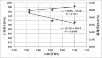
- Example 1 is a graph in which the properties of the copper alloys of Example 1 and Comparative Examples 1 and 2 are plotted against the amount of Co (mass%), and a linear approximation curve is drawn.
- the first axis represents tensile strength, and the second axis represents electrical conductivity.
- the square plots represent tensile strength, and the circle plots represent electrical conductivity.
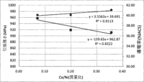
- 2 is a graph in which the properties of the copper alloys of Example 1 and Comparative Examples 1 and 2 are plotted against the mass ratio of Co to Ni, R B , and a linear approximation curve is drawn.
- the first axis represents tensile strength
- the second axis represents electrical conductivity.
- the square plots represent tensile strength, and the circle plots represent electrical conductivity.
- a to B means “greater than or equal to A and less than or equal to B," where A and B represent numerical values.
- the copper alloy of this embodiment contains 2.3 to 4.6 mass% Ni, 0.10 to 0.50 mass% Co, 0.60 to 1.3 mass% Si, 0.010 to 0.10 mass% Cr, and the balance being Cu and unavoidable impurities. That is, the copper alloy of this embodiment is a Cu-Ni-Co-Si based alloy. Ni, Co, and Si form precipitated particles of Ni-Co-Si based intermetallic compounds by appropriate heat treatment, which can achieve high electrical conductivity and high strength.
- the Ni concentration is 2.3 to 4.6 mass %
- the Co concentration is 0.10 to 0.50 mass %
- the Cr concentration is 0.010 to 0.10 mass %, which makes it possible to further improve the strength of the copper alloy while maintaining the high electrical conductivity of the copper alloy.
- the Ni concentration is less than 2.3 mass%
- the desired strength is not obtained.
- the Co concentration is less than 0.10 mass%
- the desired strength and electrical conductivity are not obtained.
- the Cr concentration is less than 0.010 mass%
- the desired strength is not obtained. If the Ni concentration exceeds 4.6 mass%, sufficient strength is obtained, but the electrical conductivity is reduced. If the Co concentration exceeds 0.50 mass%, sufficient electrical conductivity is obtained, but high strength is difficult to obtain.
- the Ni concentration is preferably 2.8 to 4.4 mass%, more preferably 3.0 to 4.0 mass%, and even more preferably 3.3 to 3.7 mass%.
- the Co concentration is preferably less than 0.50 mass%, more preferably 0.10 to 0.40 mass%, and even more preferably 0.20 to 0.30 mass%.
- the Cr concentration is preferably 0.020 to 0.070 mass%, and more preferably 0.040 to 0.060 mass%.
- the concentration of Si is 0.6 to 1.3 mass %. This allows the strength of the copper alloy to be improved while maintaining the high electrical conductivity of the copper alloy. If the concentration of Si is less than 0.60 mass %, the desired strength cannot be obtained. On the other hand, if the concentration of Si is more than 1.3 mass %, sufficient strength is obtained, but the electrical conductivity is reduced.
- the concentration of Si is preferably 0.7 to 1.2 mass %, and more preferably 0.8 to 1.0 mass %.
- Ni-Co-Si precipitates formed by Ni, Co and Si are considered to be intermetallic compounds mainly composed of (Ni+Co)Si.
- Ni, Co and Si in the copper alloy do not necessarily become precipitates by aging treatment during the manufacturing process of the copper alloy sheet, and may exist in a state of solid solution in the Cu matrix to some extent.
- Ni, Co and Si in a solid solution state can slightly improve the strength of the copper alloy sheet, the effect is smaller than that of the precipitated state, and they may be a factor in reducing the electrical conductivity. Therefore, it is preferable that the content ratio of Ni, Co and Si is close to the composition ratio of (Ni+Co)Si. Therefore, the ratio R A of the total mass of Ni and Co to Si is preferably 3.5 to 5.0, more preferably 3.5 to 4.5.
- the mass ratio R B of Co to Ni can be set to 0.010 to 0.155.
- the mass ratio R B of Co to Ni is 0.010 or more, the high electrical conductivity of the copper alloy can be maintained.
- the mass ratio R B of Co to Ni is 0.155 or less, the strength of the copper alloy can be effectively improved.
- the ratio R B is preferably from 0.025 to 0.155, and more preferably from 0.056 to 0.086.
- one or more elements selected from the group consisting of Mg, Fe, P, Cr, Ag, Zn, Sn, Pb, Zr, Al, As, Se, Te, Sb, Bi, Au, Ti, Nb, V, Ta, W, Mo, and Mn may be further contained in a total amount of 0.010 to 1.0 mass %. This can improve the strength, heat resistance, stress relaxation resistance, etc. of the copper alloy.
- the total amount of the additive elements is 0.010 mass % or more, the desired effects described above tend to be easily obtained, while when the total amount of the additive elements is 1.0 mass % or less, the desired characteristics can be obtained while preventing a decrease in electrical conductivity.
- the total amount of the added elements is preferably 0.020 to 0.080 mass %, and more preferably 0.050 to 0.080 mass %.
- the balance which is the components other than those described above, is composed of Cu and inevitable impurities.
- the inevitable impurities refer to impurity elements that are unavoidably mixed into the material during the manufacturing process.
- the concentration of each element of the inevitable impurities can be, for example, 0.015 mass% or less, and is preferably 0% (undetectable).
- the composition of the copper alloy can also be measured by wet analysis. For Ni, the copper separation dimethylglyoxime gravimetric method (JIS-H1056 (2003)) may be used, and for Si, the silicon dioxide gravimetric method (JIS-H1061 (2006)) may be used.
- ICP optical emission spectroscopy may be used, and the analysis of other added elements is performed using an internal standard method, with Y (yttrium) being used as the internal standard substance. An element other than Y may be selected as the internal standard substance.
- ICP optical emission spectroscopy the measurement is performed using an ICP optical emission spectroscopy analyzer (ICP-OES) SPS3100 manufactured by Hitachi High-Tech Science Corporation or an equivalent device.
- ICP optical emission spectroscopy a sample of the copper alloy is dissolved in a mixed acid containing hydrochloric acid and nitric acid (containing hydrochloric acid, nitric acid, and water in a volume ratio of 2:1:2) and then diluted.
- the composition of the copper alloy may be measured using X-ray fluorescence analysis.
- X-ray fluorescence analysis device Simultix 14 manufactured by Rigaku Corporation or a device equivalent thereto may be used.
- the analysis surface may be cut or mechanically polished so that the maximum surface roughness Rz (JIS-B0601 (2013)) is 6.3 ⁇ m or less.
- Rz JIS-B0601 (2013)
- a sample for X-ray fluorescence analysis is taken from the molten metal during melting and casting, it is cast into a shape of about 30 to 40 mm ⁇ and a thickness of about 50 to 80 mm, and then cut into a thickness of about 10 to 20 mm, and the cut surface is used as the analysis surface.
- X-ray fluorescence analysis is performed based on JIS K 0119:2008, and measured by a wavelength dispersion method.
- the copper alloy of this embodiment can be made into a copper alloy plate by a manufacturing method including, but not limited to, a rolling process as described below.
- the copper alloy plate is not particularly limited as long as it is an object having the above composition and a three-dimensional shape of a predetermined thickness.
- the "plate” in this copper alloy plate includes sheets, strips, and foils.
- this copper alloy plate includes not only copper alloy plates before processing for use in electronic components, but also copper alloy plates during or after processing.
- the thickness of the copper alloy plate is, for example, 0.030 to 1.2 mm. The thickness is preferably 0.050 to 0.60 mm, and more preferably 0.080 to 0.30 mm.
- the copper alloy of this embodiment has high electrical conductivity and strength due to the above-mentioned composition.
- the copper alloy of this embodiment may have a tensile strength of 870 MPa or more in a direction parallel to the rolling direction in a copper alloy sheet manufactured through a rolling process. Since it has such a high tensile strength, it is possible to suppress deformation that may occur during the manufacturing process of electronic components, specifically, during a series of processes up to the manufacturing of electronic components, including the process of manufacturing copper alloy parts (e.g., lead frames) by processing a copper alloy sheet, for miniaturized copper alloy parts for electronic components manufactured from the copper alloy or parts in the copper alloy parts.
- copper alloy parts e.g., lead frames
- the tensile strength in the direction parallel to the rolling direction is preferably 930 MPa or more, more preferably 940 MPa or more, and even more preferably 950 MPa or more.
- the upper limit of the tensile strength in the direction parallel to the rolling direction is not particularly limited, but the tensile strength may be, for example, 1200 MPa or less, 1100 MPa or less, or 1000 MPa or less.
- the tensile strength in the direction parallel to the rolling direction can be measured using a tensile tester in accordance with JIS-Z2241 (2011). Specifically, a JIS 13B test piece is prepared from each sample using a press machine so that the tensile direction is parallel to the rolling direction.
- the conditions for the tensile test are a test piece width of 12.5 mm, a measurement temperature of room temperature (15 to 35°C), a tensile speed of 5 mm/min, and a gauge length of 50 mm.
- the test is performed using two test pieces, and the average value of the two data can be used as the tensile strength in the direction parallel to the rolling direction in this disclosure.
- the above tensile speed corresponds to the crosshead displacement speed described in the JIS standard.
- the tensile tester an Autocom AC-100KN-C manufactured by TSE Co., Ltd. or an equivalent device can be used. Moreover, the tensile strength in the direction parallel to the rolling direction can be adjusted to a desired range by using the copper alloy composition of the above-mentioned copper alloy of this embodiment.
- the copper alloy of the present embodiment may have an electrical conductivity of 30% IACS or more. By having an electrical conductivity of 30% IACS or more, the copper alloy can be effectively used as a copper alloy part for electronic components. Electrical conductivity is understood to mean the electrical conductivity in the direction parallel to the rolling direction. Moreover, the electrical conductivity can be adjusted to a desired range by using the copper alloy composition according to the present embodiment described above.
- the electrical conductivity (EC: % IACS) can be measured by a four-terminal method in accordance with JIS-H0505 (1975). A double bridge is used for the measurement, and the resistance can be measured based on the average cross-sectional area method.
- the electrical conductivity can be measured at room temperature (25°C) in a direction parallel to the rolling direction. For convenience of the test sample, the gage length (distance between electrical resistance measurements) can be 50 mm.
- the copper alloy sheet can be manufactured by a method including a rolling process, although it is not particularly limited.
- the copper alloy sheet can be manufactured, for example, by homogenizing an ingot, hot rolling, intermediate cold rolling, solution treatment, aging treatment, finish cold rolling, and stress relief annealing in that order.
- Cold rolling before the solution treatment is not essential and may be performed as necessary.
- cold rolling may be performed as necessary after the solution treatment and before the aging treatment, or the solution treatment and the aging treatment may each be performed two or more times. After performing each of the above steps, grinding, polishing, shot blasting, pickling, etc. for removing oxide scale on the surface can be appropriately performed.
- the method for producing a copper alloy sheet may include a step of melting and casting a raw material of a copper alloy having the above-mentioned desired composition.
- the raw material of the copper alloy is melted in the same manner as a general copper alloy melting method, and then an ingot is produced by continuous casting or semi-continuous casting.
- an atmospheric melting furnace is first used to melt raw materials such as electrolytic copper, Ni, Co, Si, and Cr to obtain a molten metal of a desired composition. Then, the molten metal is poured into a mold of any size and cast into an ingot.
- the method for manufacturing a copper alloy sheet may include a step of hot rolling an ingot that has been subjected to an optional homogenization annealing.
- the hot rolling of the ingot is not particularly limited, but may be performed in several passes at, for example, 500 to 950°C.
- the total processing degree of the hot rolling is preferably 90% or more.
- the solution treatment is a heat treatment for dissolving silicides such as Ni-Si compounds, Co-Si compounds, and Ni-Co-Si compounds in a Cu matrix and recrystallizing the Cu matrix at the same time.
- the solution heat treatment temperature is not particularly limited, but can be, for example, 650 to 1000°C.
- the heat treatment time can be 1 second to 10 minutes. Specifically, by setting the solution treatment temperature and time to the lower limit of the above range or more, even if a large amount of silicides such as Ni-Co-Si compounds are contained in the copper alloy, they can be easily dissolved sufficiently in the Cu matrix and can be recrystallized.
- the heat treatment temperature is preferably 700 to 950° C.
- the heat treatment time is preferably 5 seconds to 5 minutes.
- the method for producing a copper alloy sheet may include a step of performing an aging treatment on the intermediate body after the above-mentioned solution treatment.
- the heat treatment temperature in the aging treatment is not particularly limited, but may be, for example, 375 to 625° C.
- the heat treatment time may be 0.5 to 50 hours.
- the tensile strength of the intermediate body after the aging treatment may be 750 MPa or more.
- the tensile strength of the intermediate body after the aging treatment may be 830 MPa or more.
- the tensile strength of the intermediate body after the aging treatment may be 850 MPa or more.
- the electrical conductivity of the intermediate body after the aging treatment in a direction parallel to the rolling direction may be 40% IACS or more.
- the aging treatment is preferably carried out in an inert atmosphere such as Ar, N 2 or H 2 in order to suppress the formation of an oxide film.
- the method for producing a copper alloy sheet may include a step of performing finish cold rolling of the intermediate body.
- the finish cold rolling is not particularly limited, but may be performed, for example, in several passes. It is preferable to perform one or more passes of rolling.
- the total processing degree of the finish cold rolling is preferably 40% or more.
- the finish cold rolling can impart processing strain to the material to improve its strength.
- the upper limit of the degree of reduction in the finish cold rolling is preferably 90% or less. By setting the degree of reduction to 90% or less, it is possible to prevent the electrical conductivity from decreasing due to processing distortion caused by strong processing.
- the degree of reduction (%) is expressed as follows: where TB is the thickness of the workpiece to be rolled and TA is the thickness of the workpiece after rolling.
- the degree of reduction (%) is expressed as: [(TB-TA)/TB] ⁇ 100.
- the method for manufacturing a copper alloy sheet may include a step of performing stress relief annealing on the intermediate body after the above-mentioned finish cold rolling.
- the stress relief annealing may be performed under general conditions, for example, at 250°C to 550°C and for a holding time of 5 seconds to 5 hours.
- the stress relief annealing may be performed in air or in an inert atmosphere such as nitrogen or argon gas.
- the copper alloy sheet after stress relief annealing may be cooled by air cooling.
- the copper alloy sheet can be manufactured by a manufacturing method including the above steps.
- pickling, polishing, degreasing, facing, and trimming may be performed as necessary after each rolling step and each heat treatment step.
- This manufacturing method may also include rolling steps and heat treatment steps other than those described above.
- the electronic component of this embodiment is an electronic component containing the copper alloy of this embodiment described above. More specifically, the electronic component of this embodiment has a copper alloy component manufactured from the copper alloy of this embodiment via a copper alloy plate inside. An example of the electronic component is a semiconductor package.
- the fine copper alloy component that can be manufactured from the copper alloy of this embodiment has a characteristic of suppressing deformation during the manufacturing process of the electronic component, so that it is suitable to use the copper alloy of this embodiment for manufacturing a semiconductor package having many fine structures.
- the semiconductor package can be manufactured, for example, but not limited to, by manufacturing a lead frame using a copper alloy plate manufactured from the copper alloy of this embodiment, supporting and fixing a semiconductor element on the lead frame, wire-bonding the semiconductor element and the leads to form internal wiring, and sealing the semiconductor element with a predetermined resin member.
- the electronic component of this embodiment may contain the copper alloy of this embodiment.
- a first aspect of the present disclosure is a copper alloy containing 2.3 to 4.6 mass% Ni, 0.10 to 0.50 mass% Co, 0.60 to 1.3 mass% Si, 0.010 to 0.10 mass% Cr, and the balance being Cu and unavoidable impurities.
- the second aspect of the present disclosure is the copper alloy described in the first aspect, containing less than 0.50 mass % Co.
- the third aspect of the present disclosure is a copper alloy according to the first or second aspect, containing 0.10 to 0.40 mass % Co.
- the fourth aspect of the present disclosure is a copper alloy according to any one of the first to third aspects, containing 0.20 to 0.30 mass % Co.
- the fifth aspect of the present disclosure is a copper alloy according to any one of the first to fourth aspects, containing 0.020 to 0.070 mass % Cr.
- the sixth aspect of the present disclosure is a copper alloy according to any one of the first to fifth aspects, containing 3.0 to 4.0 mass % Ni.
- a seventh aspect of the present disclosure is the copper alloy according to any one of the first to sixth aspects, wherein a ratio R of the total mass of Ni and Co to Si is 3.5 to 5.0.
- An eighth aspect of the present disclosure is the copper alloy according to the seventh aspect, wherein the ratio R is 3.5 to 4.5.
- a ninth aspect of the present disclosure is the copper alloy according to any one of the first to eighth aspects, wherein a mass ratio R of Co to Ni is 0.010 to 0.155.
- a tenth aspect of the present disclosure is the copper alloy according to the ninth aspect, wherein the ratio R is 0.025 to 0.155.
- An eleventh aspect of the present disclosure is the copper alloy according to the ninth aspect, wherein the ratio R is 0.056 to 0.086.
- a twelfth aspect of the present disclosure is a copper alloy according to any one of the first to eleventh aspects, further containing 0.010 to 1.0 mass% in total of one or more elements selected from the group consisting of Mg, Fe, P, Cr, Ag, Zn, Sn, Pb, Zr, Al, As, Se, Te, Sb, Bi, Au, Ti, Nb, V, Ta, W, Mo, and Mn.
- the thirteenth aspect of the present disclosure is a copper alloy according to any one of the first to twelfth aspects, which has a conductivity of 30% IACS or more.
- the fourteenth aspect of the present disclosure is a copper alloy according to any one of the first to thirteenth aspects, in which the tensile strength in the direction parallel to the rolling direction is 870 MPa or more.
- the fifteenth aspect of the present disclosure is a copper alloy according to any one of the first to fourteenth aspects, in which the tensile strength in the direction parallel to the rolling direction is 930 MPa or more.
- the sixteenth aspect of the present disclosure is an electronic component that includes the copper alloy described in any one of the first to fifteenth aspects.
- Example 1 a copper alloy sheet was prepared from a desired copper alloy as follows. Using electrolytic copper as a raw material, copper alloys having the compositions shown in Table 1 were melted and cast in an atmospheric melting furnace. The ingots were hot rolled at 950° C. to a plate thickness of 10.0 mm. After hot rolling, the plates were faced and then intermediate cold rolled to a plate thickness of 0.167 mm. Thereafter, solution treatment and aging treatment were performed under the conditions shown in Table 1. Next, the sheets were finish cold-rolled to a thickness of 0.1 mm with a working ratio shown in Table 1 to obtain copper alloy sheets.
- Example 2 the copper alloy sheet subjected to the finish cold rolling in Example 1 was further subjected to stress relief annealing in air under the conditions shown in Table 2. The copper alloy sheet after stress relief annealing was cooled by air cooling to obtain the copper alloy sheet of Example 2.
- Comparative Examples 1 and 2 copper alloy sheets were manufactured in the same manner as in Example 1, except that the composition of the copper alloy and the solution treatment conditions were changed to those shown in Table 1. Specifically, in Comparative Example 1, the composition of the copper alloy was changed to that shown in Table 1, and the solution treatment temperature was changed to 900 ° C. or 925 ° C. as shown in Table 1. Two samples were manufactured as copper alloy sheets by the same manufacturing method as in Example 1.
- each copper alloy in Comparative Example 1 was performed by plotting the numerical values of the evaluation results of the two samples (tensile strength and electrical conductivity for the intermediate body after aging treatment and the copper alloy sheet after finish cold rolling as shown in Table 1) on the vertical axis and the solution treatment temperature on the horizontal axis, calculating a straight line connecting the plots, and then substituting the value of the solution treatment temperature of 915 ° C. into the formula representing the straight line, thereby obtaining each estimated evaluation result of the copper alloy and its intermediate when the solution treatment was performed at 915 ° C.
- Comparative Example 2 similarly to Comparative Example 1, the composition of the copper alloy was changed to that shown in Table 1, and the solution treatment temperature was changed to 910 ° C, 935 ° C, and 950 ° C as shown in Table 1. Except for this, three samples were manufactured as copper alloy sheets by the same manufacturing method as in Example 1.
- the evaluation of each copper alloy in Comparative Example 2 was carried out by plotting the numerical values of the evaluation results of the three samples on the vertical axis and the solution treatment temperature on the horizontal axis, calculating an approximate line connecting the plots (using the approximate line function of Microsoft Excel (registered trademark)), and then substituting the value of the solution treatment temperature of 915 ° C into the formula representing the approximate line, thereby obtaining each estimated evaluation result of the copper alloy and its intermediate when the solution treatment was carried out at 915 ° C.
- the obtained copper alloy sheets of Examples 1 and 2 and the copper alloy sheets of Comparative Examples 1 and 2 were subjected to the following measurements. The results are shown in Tables 1 and 2.
- ⁇ composition ⁇ The composition of the obtained copper alloy was confirmed by X-ray fluorescence analysis. A Simultix 14 manufactured by Rigaku Corporation was used as the X-ray fluorescence analyzer. The analysis surface was cut or mechanically polished so that the maximum surface roughness Rz (JIS-B0601 (2013)) was 6.3 ⁇ m or less. X-ray fluorescence analysis was performed based on JIS K 0119:2008 and measured by a wavelength dispersion method.
- TS tensile strength
- the tensile strength (TS) of the obtained copper alloy sheet was measured in a direction parallel to the rolling direction using a tensile tester in accordance with JIS-Z2241 (2011). Specifically, a JIS 13B test piece was prepared from each sample using a press so that the tensile direction was parallel to the rolling direction. The conditions for the tensile test were a test piece width of 12.5 mm, a measurement temperature of room temperature (15 to 35°C), a tensile speed (crosshead displacement speed) of 5 mm/min, and a gauge length of 50 mm. The test was performed using two test pieces, and the average values of the two data are shown in Tables 1 and 2.
- ⁇ conductivity ⁇ Electrical conductivity (EC: % IACS) was measured by a four-terminal method in accordance with JIS-H0505 (1975). A double bridge was used for the measurement, and resistance was measured based on the average cross-sectional area method. Electrical conductivity was measured in a direction parallel to the rolling direction at room temperature (25°C). The gage length (distance between electrical resistance measurements) was 50 mm.
- the properties (tensile strength and electrical conductivity) of the copper alloys of Example 1, Comparative Example 1, and Comparative Example 2 were plotted against the mass ratio R B of Co to Ni (Co/Ni (mass ratio)), and the results of drawing a linear approximation curve are shown in FIG. 2. It is considered that as R B increases, Co-Si-based precipitates or Ni-Co-Si-based precipitates are generated, making it easier to obtain electrical conductivity and harder to obtain strength. Therefore, a linear approximation curve was created from the experimental values obtained in the examples, and the strength and electrical conductivity at each R B were predicted. From this result, it can be seen that if the ratio R B is 0.010 or more, electrical conductivity of 39.7% IACS or more can be realized.
- ratio R B is 0.025 or more, electrical conductivity of 39.7% IACS or more can be realized. If the ratio R B is 0.056 or more, electrical conductivity of 39.8% IACS or more can be realized. It can also be seen that if the ratio R B is 0.155 or less, a tensile strength of 938 MPa or more can be realized. It can be seen that if the ratio R B is 0.086 or less, a tensile strength of 949 MPa or more can be achieved.
Landscapes
- Chemical & Material Sciences (AREA)
- Engineering & Computer Science (AREA)
- Materials Engineering (AREA)
- Mechanical Engineering (AREA)
- Metallurgy (AREA)
- Organic Chemistry (AREA)
- Physics & Mathematics (AREA)
- Thermal Sciences (AREA)
- Crystallography & Structural Chemistry (AREA)
- Conductive Materials (AREA)
Priority Applications (3)
| Application Number | Priority Date | Filing Date | Title |
|---|---|---|---|
| CN202480073818.8A CN122249569A (zh) | 2023-12-07 | 2024-07-25 | 铜合金及电子部件 |
| JP2025561681A JPWO2025120904A1 (cg-RX-API-DMAC7.html) | 2023-12-07 | 2024-07-25 | |
| KR1020267010691A KR20260053088A (ko) | 2023-12-07 | 2024-07-25 | 구리 합금 및 전자 부품 |
Applications Claiming Priority (2)
| Application Number | Priority Date | Filing Date | Title |
|---|---|---|---|
| JP2023207165A JP7648724B1 (ja) | 2023-12-07 | 2023-12-07 | 銅合金及び電子部品 |
| JP2023-207165 | 2023-12-07 |
Publications (1)
| Publication Number | Publication Date |
|---|---|
| WO2025120904A1 true WO2025120904A1 (ja) | 2025-06-12 |
Family
ID=95019438
Family Applications (1)
| Application Number | Title | Priority Date | Filing Date |
|---|---|---|---|
| PCT/JP2024/026687 Pending WO2025120904A1 (ja) | 2023-12-07 | 2024-07-25 | 銅合金及び電子部品 |
Country Status (5)
| Country | Link |
|---|---|
| JP (2) | JP7648724B1 (cg-RX-API-DMAC7.html) |
| KR (1) | KR20260053088A (cg-RX-API-DMAC7.html) |
| CN (1) | CN122249569A (cg-RX-API-DMAC7.html) |
| TW (1) | TWI911835B (cg-RX-API-DMAC7.html) |
| WO (1) | WO2025120904A1 (cg-RX-API-DMAC7.html) |
Citations (6)
| Publication number | Priority date | Publication date | Assignee | Title |
|---|---|---|---|---|
| JP2007107062A (ja) * | 2005-10-14 | 2007-04-26 | Nikko Kinzoku Kk | 電子材料用Cu−Ni−Si系銅合金 |
| WO2009123137A1 (ja) * | 2008-03-31 | 2009-10-08 | 日鉱金属株式会社 | 電子材料用Cu-Ni-Si-Co-Cr系合金 |
| JP2015183263A (ja) * | 2014-03-25 | 2015-10-22 | Dowaメタルテック株式会社 | Cu−Ni−Co−Si系銅合金板材およびその製造方法並びに通電部品 |
| JP2016176105A (ja) * | 2015-03-19 | 2016-10-06 | Jx金属株式会社 | 電子部品用Cu−Ni−Co−Si合金 |
| JP2018145495A (ja) * | 2017-03-07 | 2018-09-20 | Jx金属株式会社 | 電子部品用Cu−Ni−Co−Si合金 |
| JP2023100244A (ja) * | 2022-01-05 | 2023-07-18 | Dowaメタルテック株式会社 | Cu-[Ni,Co]-Si系銅合金板材、その製造方法、通電部品および放熱部品 |
Family Cites Families (2)
| Publication number | Priority date | Publication date | Assignee | Title |
|---|---|---|---|---|
| JP5776833B1 (ja) | 2014-08-29 | 2015-09-09 | 三菱マテリアル株式会社 | 電子・電気機器用銅合金、電子・電気機器用銅合金薄板、電子・電気機器用部品及び端子 |
| WO2017168803A1 (ja) | 2016-03-31 | 2017-10-05 | Dowaメタルテック株式会社 | Cu-Ni-Si系銅合金板材および製造法 |
-
2023
- 2023-12-07 JP JP2023207165A patent/JP7648724B1/ja active Active
-
2024
- 2024-07-25 WO PCT/JP2024/026687 patent/WO2025120904A1/ja active Pending
- 2024-07-25 CN CN202480073818.8A patent/CN122249569A/zh active Pending
- 2024-07-25 KR KR1020267010691A patent/KR20260053088A/ko active Pending
- 2024-07-25 JP JP2025561681A patent/JPWO2025120904A1/ja active Pending
- 2024-08-06 TW TW113129397A patent/TWI911835B/zh active
Patent Citations (6)
| Publication number | Priority date | Publication date | Assignee | Title |
|---|---|---|---|---|
| JP2007107062A (ja) * | 2005-10-14 | 2007-04-26 | Nikko Kinzoku Kk | 電子材料用Cu−Ni−Si系銅合金 |
| WO2009123137A1 (ja) * | 2008-03-31 | 2009-10-08 | 日鉱金属株式会社 | 電子材料用Cu-Ni-Si-Co-Cr系合金 |
| JP2015183263A (ja) * | 2014-03-25 | 2015-10-22 | Dowaメタルテック株式会社 | Cu−Ni−Co−Si系銅合金板材およびその製造方法並びに通電部品 |
| JP2016176105A (ja) * | 2015-03-19 | 2016-10-06 | Jx金属株式会社 | 電子部品用Cu−Ni−Co−Si合金 |
| JP2018145495A (ja) * | 2017-03-07 | 2018-09-20 | Jx金属株式会社 | 電子部品用Cu−Ni−Co−Si合金 |
| JP2023100244A (ja) * | 2022-01-05 | 2023-07-18 | Dowaメタルテック株式会社 | Cu-[Ni,Co]-Si系銅合金板材、その製造方法、通電部品および放熱部品 |
Also Published As
| Publication number | Publication date |
|---|---|
| KR20260053088A (ko) | 2026-04-20 |
| TWI911835B (zh) | 2026-01-11 |
| JPWO2025120904A1 (cg-RX-API-DMAC7.html) | 2025-06-12 |
| JP2025091735A (ja) | 2025-06-19 |
| JP7648724B1 (ja) | 2025-03-18 |
| CN122249569A (zh) | 2026-06-19 |
| TW202523867A (zh) | 2025-06-16 |
Similar Documents
| Publication | Publication Date | Title |
|---|---|---|
| CN114787400B (zh) | 铜合金、铜合金塑性加工材、电子电气设备用组件、端子、汇流条及散热基板 | |
| TWI387657B (zh) | Cu-Ni-Si-Co based copper alloy for electronic materials and method of manufacturing the same | |
| CN101113499A (zh) | 具有高强度和高抗软化性的铜合金 | |
| JP4834781B1 (ja) | 電子材料用Cu−Co−Si系合金 | |
| CN114302975B (zh) | 电子电气设备用铜合金﹑电子电气设备用铜合金板条材、电子电气设备用组件、端子及汇流排 | |
| KR20180125446A (ko) | 전자·전기 기기용 구리 합금, 전자·전기 기기용 구리 합금판 조재, 전자·전기 기기용 부품, 단자, 버스바, 및 릴레이용 가동편 | |
| JP5871443B1 (ja) | 銅合金板材およびその製造方法 | |
| KR102599762B1 (ko) | 전기전도도 특성이 우수한 알루미늄 다이캐스팅 합금, 이를 이용한 주조품 및 이의 제조방법 | |
| US11319615B2 (en) | Copper alloy for electronic and electrical equipment, copper alloy plate strip for electronic and electrical equipment, component for electronic and electrical equipment, terminal, busbar, and movable piece for relay | |
| JP2010285671A (ja) | 高強度高導電性銅合金とその製造方法 | |
| JP7648724B1 (ja) | 銅合金及び電子部品 | |
| JP7300049B1 (ja) | リードフレーム素形体を製造する方法及び半導体パッケージを製造する方法 | |
| JP2012229467A (ja) | 電子材料用Cu−Ni−Si系銅合金 | |
| WO2025120905A1 (ja) | 銅合金板、電子部品及び銅合金板の製造方法 | |
| WO2025120908A1 (ja) | 銅合金板、電子部品及び銅合金板の製造方法 | |
| WO2025120909A1 (ja) | 銅合金板、電子部品及び銅合金板の製造方法 | |
| WO2025120906A1 (ja) | 銅合金板、電子部品及び銅合金板の製造方法 | |
| US20070131321A1 (en) | Copper alloy for electric and electronic instruments | |
| JP2013117060A (ja) | 電子材料用Cu−Co−Si系合金 | |
| WO2025120939A1 (ja) | 銅合金板、電子部品及び銅合金板の製造方法 | |
| WO2026048037A1 (ja) | 銅合金板、電子部品及び銅合金板の製造方法 | |
| JP7736077B2 (ja) | 銅合金、銅合金塑性加工材、電子・電気機器用部品、端子、バスバー、リードフレーム | |
| JP2012167347A (ja) | 高強度銅合金鍛造材 | |
| JP2012229469A (ja) | 電子材料用Cu−Si−Co系銅合金及びその製造方法 | |
| JP4349631B2 (ja) | 電機、電子機器部品用コルソン合金細線の製造方法 |
Legal Events
| Date | Code | Title | Description |
|---|---|---|---|
| 121 | Ep: the epo has been informed by wipo that ep was designated in this application |
Ref document number: 24900202 Country of ref document: EP Kind code of ref document: A1 |
|
| ENP | Entry into the national phase |
Ref document number: 2025561681 Country of ref document: JP Kind code of ref document: A |
|
| WWE | Wipo information: entry into national phase |
Ref document number: 2025561681 Country of ref document: JP |
|
| ENP | Entry into the national phase |
Ref document number: 1020267010691 Country of ref document: KR Free format text: ST27 STATUS EVENT CODE: A-0-1-A10-A15-NAP-PA0105 (AS PROVIDED BY THE NATIONAL OFFICE) |
|
| WWE | Wipo information: entry into national phase |
Ref document number: 1020267010691 Country of ref document: KR |
|
| WWP | Wipo information: published in national office |
Ref document number: 1020267010691 Country of ref document: KR |
|
| NENP | Non-entry into the national phase |
Ref country code: DE |