WO2025115517A1 - 積層型電子部品 - Google Patents
積層型電子部品 Download PDFInfo
- Publication number
- WO2025115517A1 WO2025115517A1 PCT/JP2024/039043 JP2024039043W WO2025115517A1 WO 2025115517 A1 WO2025115517 A1 WO 2025115517A1 JP 2024039043 W JP2024039043 W JP 2024039043W WO 2025115517 A1 WO2025115517 A1 WO 2025115517A1
- Authority
- WO
- WIPO (PCT)
- Prior art keywords
- base electrode
- cover
- electrode
- thickness
- electronic component
- Prior art date
- Legal status (The legal status is an assumption and is not a legal conclusion. Google has not performed a legal analysis and makes no representation as to the accuracy of the status listed.)
- Pending
Links
Images


Classifications
-
- H—ELECTRICITY
- H01—ELECTRIC ELEMENTS
- H01G—CAPACITORS; CAPACITORS, RECTIFIERS, DETECTORS, SWITCHING DEVICES, LIGHT-SENSITIVE OR TEMPERATURE-SENSITIVE DEVICES OF THE ELECTROLYTIC TYPE
- H01G4/00—Fixed capacitors; Processes of their manufacture
- H01G4/30—Stacked capacitors
-
- H—ELECTRICITY
- H01—ELECTRIC ELEMENTS
- H01G—CAPACITORS; CAPACITORS, RECTIFIERS, DETECTORS, SWITCHING DEVICES, LIGHT-SENSITIVE OR TEMPERATURE-SENSITIVE DEVICES OF THE ELECTROLYTIC TYPE
- H01G4/00—Fixed capacitors; Processes of their manufacture
- H01G4/002—Details
- H01G4/005—Electrodes
- H01G4/012—Form of non-self-supporting electrodes
-
- H—ELECTRICITY
- H01—ELECTRIC ELEMENTS
- H01G—CAPACITORS; CAPACITORS, RECTIFIERS, DETECTORS, SWITCHING DEVICES, LIGHT-SENSITIVE OR TEMPERATURE-SENSITIVE DEVICES OF THE ELECTROLYTIC TYPE
- H01G4/00—Fixed capacitors; Processes of their manufacture
- H01G4/002—Details
- H01G4/018—Dielectrics
- H01G4/06—Solid dielectrics
- H01G4/08—Inorganic dielectrics
- H01G4/12—Ceramic dielectrics
- H01G4/1209—Ceramic dielectrics characterised by the ceramic dielectric material
-
- H—ELECTRICITY
- H01—ELECTRIC ELEMENTS
- H01G—CAPACITORS; CAPACITORS, RECTIFIERS, DETECTORS, SWITCHING DEVICES, LIGHT-SENSITIVE OR TEMPERATURE-SENSITIVE DEVICES OF THE ELECTROLYTIC TYPE
- H01G4/00—Fixed capacitors; Processes of their manufacture
- H01G4/002—Details
- H01G4/224—Housing; Encapsulation
-
- H—ELECTRICITY
- H01—ELECTRIC ELEMENTS
- H01G—CAPACITORS; CAPACITORS, RECTIFIERS, DETECTORS, SWITCHING DEVICES, LIGHT-SENSITIVE OR TEMPERATURE-SENSITIVE DEVICES OF THE ELECTROLYTIC TYPE
- H01G4/00—Fixed capacitors; Processes of their manufacture
- H01G4/002—Details
- H01G4/228—Terminals
- H01G4/232—Terminals electrically connecting two or more layers of a stacked or rolled capacitor
Definitions
- This disclosure relates to multilayer electronic components such as multilayer ceramic capacitors.
- a known example of a multilayer electronic component is a multilayer ceramic capacitor (see, for example, Patent Documents 1 and 2 below).
- a multilayer ceramic capacitor has, for example, a main body that directly functions as a capacitor, and external electrodes for mounting the capacitor on a circuit board or the like.
- the main body has alternatingly stacked dielectric layers and flat internal electrodes. The edges of the internal electrodes are exposed from the side surfaces of the main body (surfaces along the stacking direction).
- the external electrodes are, for example, made of metal layers, and cover the side surfaces of the main body as well as the areas of the upper and lower surfaces of the main body that are close to the side surfaces.
- Patent Document 1 discloses a capacitor in which the side surfaces of the main body are formed in a concave shape.
- base electrodes are provided on the side, top, and bottom surfaces of the main body, and metal is deposited on the base electrodes by plating, thereby forming external electrodes.
- the multilayer electronic component has an effective portion, a first cover, and a first base electrode.
- the effective portion has dielectric layers and internal electrodes alternately stacked in a stacking direction.
- the first cover overlaps the effective portion from the first side of the first and second sides in the stacking direction.
- the first base electrode overlaps the first cover from the first side.
- the effective portion has an end face facing the third side of the third and fourth sides in a first direction intersecting the stacking direction.
- the multiple internal electrodes include two or more internal electrodes each having an exposed edge portion exposed from the end face.
- the first base electrode is located in the third side region of the first side surface of the first cover.
- the exposed edges are different from one another in the first direction.
- the position of the exposed edge that is furthest to the fourth side among the exposed edges is referred to as the innermost position
- the edge on the third side of the first base electrode is located at the same position as the innermost position or on the fourth side of the innermost position.
- the first end face on the third side of the first base electrode is inclined with respect to the stacking direction so that the first side is closer to the fourth side.
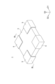
- FIG. 1 is a perspective view showing a capacitor according to a first embodiment.
- FIG. 2 is a schematic exploded perspective view of the capacitor of FIG. 1 .
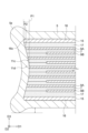
- FIG. 2 is a cross-sectional view taken along line III-III in FIG.
- FIG. 4 is an enlarged view of region IV in FIG. 3 .
- FIG. 11 is a cross-sectional view showing another example of a side surface of a capacitor.
- FIG. 11 is a perspective view showing a capacitor according to a second embodiment.
- FIG. 11 is a cross-sectional view showing a side surface of a capacitor according to a comparative example.
- the corners may be chamfered with a curved surface or the like, as long as the above concept of shape is valid.
- a corner formed by two sides may be chamfered to a length of 1/5, 1/10, or 1/20 of the length of the shorter of the two sides.
- the corners may be rounded due to manufacturing precision (error). The same applies to other polygons, etc.
- the base electrode may be a layer that is essentially of constant thickness, but may have a configuration where the thickness can be considered to vary at the ends.
- this variation in thickness at the ends is not taken into account, unless otherwise specified.
- Fig. 1 is a perspective view showing a capacitor 1 (an example of a multilayer electronic component) according to a first embodiment.
- a Cartesian coordinate system D1D2D3 is attached to Fig. 1 and other figures described later.
- the capacitor 1 may be used with either side being the upper or lower.
- the +D3 side may be regarded as the upper side, and terms such as the upper surface and the lower surface may be used.
- Capacitor 1 is, for example, a multilayer ceramic capacitor. Capacitor 1 has a roughly rectangular parallelepiped body 3 and four external electrodes 5 located at the four corners of body 3 in a plan view (as viewed in the D3 direction). The external electrodes 5 contribute to the electrical connection between capacitor 1 and other electronic components (for example, a circuit board not shown).
- FIG. 3 is a cross-sectional view taken along line III-III in FIG. 1.
- FIG. 3 shows a D1D3 cross-section taken through the external electrode 5 on the +D2 side.
- the D1D3 cross-section taken through the external electrode 5 on the -D2 side, the D2D3 cross-section taken through the external electrode 5 on the -D1 side, and the D2D3 cross-section taken through the external electrode 5 on the +D1 side are basically the same.
- the terms D1, D2, and D3 may be used to explain the positional relationships between the components, without any particular mention, assuming the cross-section shown in FIG. 3.
- the main body 3 has, for example, an effective portion 11, two covers 13 respectively overlapping the upper and lower surfaces of the effective portion 11, and an undercoat layer 15 overlapping the surface of each cover 13 opposite the effective portion 11.
- the effective portion 11 has a plurality of dielectric layers 7 and a plurality of internal electrodes 9 which are alternately overlapped.
- the multiple internal electrodes 9 include a plurality of first internal electrodes 9A and a plurality of second internal electrodes 9B.
- Each undercoat layer 15 has, for example, four undercoat electrodes 16 at positions corresponding to the positions of the four external electrodes 5.
- the active portion 11 directly functions as a capacitor.
- the cover 13 contributes, for example, to protecting the main body portion 3 and improving its strength.
- the base electrode 16 contributes, for example, to depositing the metal that will become the external electrode 5 by plating and/or improving the adhesive strength of the external electrode 5 to the main body portion 3.
- the side facing the -D1 side is referred to as the end face 11c.
- the -D1 side can be said to be one side (an example of the third side) in a direction (D1 direction) intersecting the stacking direction (D3 direction) of the dielectric layers 7 and the internal electrodes 9.
- a part of the edge of the first internal electrode 9A (sometimes referred to as the exposed edge 9c) is exposed from the end face 11c.
- the external electrode 5 on the -D1 side covers the end face 11c and is fixed to the exposed edge 9c. This electrically connects the first internal electrode 9A and the external electrode 5.
- FIG. 4 is an enlarged view of region IV in FIG. 3.
- End surface 11c has, for example, a concave portion 11d recessed toward the +D1 side.
- the position of the exposed edge portion 9c located furthest toward the +D1 side (an example of the fourth side) among the exposed edge portions 9c is referred to as the innermost position P1.
- the edge portion on the -D1 side of base electrode 16 (an example of a first base electrode) on the +D3 side (and -D1 side) is located at the same position as innermost position P1, or on the +D1 side of innermost position P1.
- base electrode 16 an example of a second base electrode
- the likelihood of a protrusion 5z (see FIG. 7) being formed on the external electrode 5 is reduced.
- the likelihood of poor alignment caused by the protrusion 5z is reduced.
- the likelihood of the capacitor 1 being subjected to an unintended force from the circuit board is reduced.
- the likelihood of a crack occurring in the external electrode 5 is reduced.
- the end face 16c (an example of a first end face) on the -D1 side (an example of a third side) of the base electrode 16 (an example of a first base electrode) on the +D3 side (an example of a first side) is inclined with respect to the D3 direction (an example of a stacking direction) in a direction that positions it closer to the +D3 side (an example of a fourth side).
- Such features may be extracted.
- the probability of the formation of the protrusion 5z is reduced, for example, as described in detail later.
- the same or similar effect as that caused by the above-mentioned positional relationship between the edge of the base electrode 16 and the innermost position P1 is achieved.
- the probability of the formation of the protrusion 5z is further reduced.
- the above-mentioned positional relationship between the base electrode 16 and the innermost position P1 may or may not hold. Furthermore, at least some (two or more) of the multiple exposed edges 9c may have different positions in the D1 direction or may be the same as each other.
- (1.1. Configuration of the Capacitor According to the First Embodiment) (1.1. Overall configuration) 1 is configured as, for example, a surface-mounted chip-type component. Specifically, for example, the capacitor 1 is placed with its -D3 side or +D3 side facing a circuit board (not shown). Then, the four pads of the circuit board and the four external electrodes 5 are respectively joined with a conductive bonding material (e.g., solder) (not shown), thereby mounting the capacitor on the circuit board.
- a conductive bonding material e.g., solder
- the configuration (internal structure and external shape) of capacitor 1 is, for example, roughly plane-symmetric with respect to a plane of symmetry (not shown) that is parallel to the D1D2 plane and passes through the center of capacitor 1 in the thickness direction (D3 direction).
- the configuration of capacitor 1 is, for example, rotationally symmetric by 180° when viewed in the D3 direction.
- capacitor 1 does not have to have such symmetry.
- the shape of the main body 3 is, for example, roughly a thin rectangular parallelepiped.
- This rectangular parallelepiped may be a square (as in the illustrated example) or a rectangle (excluding a square; the same applies below) in plan view.
- a square shape may be assumed unless otherwise specified.
- the specific dimensions of the main body 3 (or the capacitor 1) are arbitrary. As an example of dimensions when the capacitor 1 is relatively small, the lengths of the main body 3 (or the capacitor 1) in the D1 and D2 directions may each be 0.030 mm or more and 0.200 mm or less. When the length in the D1 direction is L and the length in the D2 direction is W, L/W may be 0.5 or more and 2.0 or less. The thickness in the D3 direction may be 0.030 mm or more and 0.200 mm or less. When the surface of the main body 3 is not flat, for example, the maximum values of the various dimensions may satisfy the above ranges (the same applies below to the various dimensions of the other components, unless a contradiction arises).
- the example dimensions of each component described below are for a relatively small capacitor 1. Therefore, dimensions larger (or smaller) than the example dimensions may be used.
- Multiple components of the same type may basically (except for relatively small differences, for example; the same applies below) be provided with the same (or corresponding) shape, size, material, position, etc., unless otherwise specified or unless a contradiction occurs. Therefore, unless otherwise specified or unless a contradiction occurs, a description of one component may be considered to be common to multiple components of the same type.
- a single layered (membrane-like) component may be entirely made of one type of material. However, it may also be made of layers made of different materials.
- the shape of the effective portion 11 shown in FIG. 3 is, for example, approximately a thin rectangular parallelepiped. Its planar shape is basically the same as that of the main body portion 3.
- the specific thickness of the effective portion 11 is arbitrary.
- the thickness of the effective portion 11 may be 30% or more, 40% or more, or 50% or more, or 90% or less, 80% or less, or 70% or less, relative to the thickness of the main body portion 3.
- the above lower limit and upper limit may be combined with any one of them.
- the thickness of the main body portion 3 is, for example, the thickness from the upper surface of the upper base electrode 16 to the lower surface of the lower base electrode 16.
- the thickness of the effective portion 11 is, for example, the thickness from the upper surface of the internal electrode 9 of the uppermost layer to the lower surface of the internal electrode 9 of the lowermost layer.
- the dielectric layer 7 is basically a layer having a constant thickness (at least between the internal electrodes 9).
- the thickness of the dielectric layer 7 may be set appropriately depending on the characteristics required of the capacitor 1.
- the thickness between adjacent internal electrodes 9 may be 0.1 ⁇ m or more or 0.5 ⁇ m or more, and may be 3.0 ⁇ m or less, 2.0 ⁇ m or less, or 1.0 ⁇ m or less.
- the above lower and upper limits may be combined with any combination.
- the shape and dimensions of the dielectric layer 7 in a planar view are basically the same as the shape and dimensions of the active part 11 in a planar view.
- the material of the dielectric layer is, for example, ceramics, and the specific type is also arbitrary.
- the number of layers of the dielectric layer 7 (internal electrodes 9) is arbitrary. One example is 10 layers or more and 30 layers or less.
- the internal electrode 9 is a layer having a certain thickness.
- the thickness of the internal electrode 9 is arbitrary, and may be thinner, the same as, or thicker than the thickness of the region of the dielectric layer 7 between the internal electrodes 9.
- the thickness of the internal electrode 9 may be 0.3 ⁇ m or more or 0.5 ⁇ m or more, and may be 3.0 ⁇ m or less, 2.0 ⁇ m or less, or 1.0 ⁇ m or less.
- the above lower and upper limits may be combined with any combination.
- the material of the internal electrode 9 is, for example, a metal.
- the specific type of metal is arbitrary, and for example, all or the main component (for example, 60 mass% or more of a component; the same applies below) is a base metal (for example, Ni and/or Cu).
- FIG. 2 is an exploded perspective view of the capacitor 1.
- FIG. 2 is a schematic diagram for understanding the shape and relative positions of the internal electrodes 9, etc. Therefore, FIG. 2 shows a smaller number of different layers than FIG. 3.
- the internal electrode 9 has, for example, a rectangular (square in the illustrated example) electrode body 9a in a plan view, and a pair of extraction electrodes 9b extending from a pair of opposing corners of the electrode body 9a.
- the electrode body 9a is located inside the outer edge of the dielectric layer 7 and is not exposed from the side of the active portion 11.
- the pair of extraction electrodes 9b reach the outer edge of the dielectric layer 7 and are connected to a pair of external electrodes 5 located at a pair of opposing corners of the main body portion 3.
- the first internal electrode 9A and the second internal electrode 9B face each other with the dielectric layer 7 in between.
- a pair of extraction electrodes 9b of the first internal electrode 9A and a pair of extraction electrodes 9b of the second internal electrode 9B are located on different diagonals in a plan view. Both are connected to a pair of external electrodes 5 that are different from each other.
- the various dimensions of the electrode body 9a and the extraction electrode 9b are arbitrary.
- the length of the extraction electrode 9b on one side of the dielectric layer 7 i.e., the length of the exposed edge 9c
- the length of the external electrode 5 along the above-mentioned one side is approximately the same as the length of the external electrode 5 along the above-mentioned one side.
- the cover 13 shown in FIG. 3 is, for example, a layer having a shape and dimensions that overlap the effective portion 11 without excess or deficiency.
- the thickness of the cover 13 is approximately constant in each of the arrangement region and non-arrangement region of the base electrode 16.
- the ratio of the thickness of the cover 13 to the thickness of the main body portion 3 may be approximately the reverse of the ratio of the thickness of the effective portion 11 to the thickness of the main body portion 3 (as described above).
- the thickness of one cover 13 may be, for example, 5% or more, 10% or more, or 15% or more of the thickness of the main body portion 3, and may be 35% or less, 30% or less, or 25% or less.
- the above lower limit and upper limit may be combined arbitrarily.
- the thickness of the cover 13 is, for example, the thickness in a region that overlaps the internal electrode 9 and does not overlap the base electrode 16 (not crushed by the base electrode 16).
- Each cover 13 has, for example, multiple (two in the example of FIG. 3) insulating layers 17 and at least one (one in the example of FIG. 3) dummy layer 19 located between the multiple insulating layers 17.
- Each dummy layer 19 has, for example, four dummy electrodes 20 at positions corresponding to the positions of the four external electrodes 5.
- the dummy electrodes 20 contribute, for example, to reinforcing the cover 13 and/or improving the connection strength between the main body 3 and the external electrodes 5, and also function as a base for the external electrodes 5 in an embodiment in which the external electrodes 5 are formed by plating.
- the cover 13 may have only one or more insulating layers 17 (it may not have a dummy layer 19).
- the insulating layers 17 and the dummy layers 19 are alternately stacked one on top of the other.
- the dummy layers 19 are provided at the boundaries of all the insulating layers 17.
- the dummy layers 19 may be provided only at some of the boundaries.
- the dummy layers 19 may not be provided at one or more boundaries that are relatively close to the active portion 11, and the dummy layers 19 may be provided only at one or more boundaries that are relatively far from the active portion 11.
- two or more insulating layers 17 that are in close contact with each other without a dummy layer 19 in between may be regarded as one insulating layer 17.
- the insulating layer 17 is a layer having a generally constant thickness, except for variations in thickness resulting from the presence or absence of overlap with the conductor layers (9, 15, and 19).
- the planar shape of the insulating layer 17 is, for example, basically the same as the planar shape of the dielectric layer 7.
- the material of the insulating layer 17 is arbitrary.
- the material of the insulating layer 17 may be the same as the material of the dielectric layer 7, or may be different.
- the material of the insulating layer 17 may be, for example, ceramics, or a material other than ceramics.
- the thickness of the insulating layer 17 is arbitrary.
- the thickness of the insulating layer 17 may be thicker (as in the illustrated example), equal to, or thinner than the thickness of the dielectric layer 7 (both are the thickness between the conductor layers, or the thickness of the area not overlapping the conductor layers. The same applies below in this paragraph).
- the thickness of the insulating layer 17 may be 2 times or more, 3 times or more, or 5 times or more, or 20 times or less, 10 times or less, or 5 times or less, of the thickness of the dielectric layer 7.
- the above lower and upper limits may be combined in any combination.
- the thickness of the insulating layer 17 may be 1.0 ⁇ m or more, or 2.0 ⁇ m or more, and 10.0 ⁇ m or less, or 5.0 ⁇ m or less.
- the above lower and upper limits may be combined in any combination.
- the insulating layer overlapping the uppermost internal electrode 9 may be regarded as the insulating layer 17, not the dielectric layer 7, regardless of its material and thickness. The same applies to the insulating layer that overlaps the bottom-most internal electrode 9.
- the dummy electrode 20 is, for example, a layer having a basically constant thickness.
- the material of the dummy electrode 20 is, for example, a metal.
- the specific type of metal is arbitrary, and for example, the entire or main component is a base metal (for example, Ni and/or Cu).
- the material of the dummy electrode 20 may be the same as the material of the internal electrode 9, or may be different.
- the position, shape, and size of the dummy electrode 20 are arbitrary. In the example of FIG. 2 and FIG. 3, the position, shape, and size of the dummy electrode 20 are set to a position, shape, and size that approximately overlaps with the external electrode 5 in a plan view (however, the external electrode 5 is slightly wider).
- the dummy electrode 20 is exposed, for example, on the side of the main body 3. This exposed portion is fixed to the external electrode 5.
- the thickness of the dummy electrode 20 is arbitrary.
- the thickness of the dummy electrode 20 may be thicker than the thickness of the internal electrode 9 (as shown in the example), may be approximately the same as the thickness of the internal electrode 9, or may be thinner.
- the thickness of the dummy electrode 20 may be 1 time or more, 1.5 times or more, or 2 times or more, or may be 10 times or less, 5 times or less, or 2 times or less, of the thickness of the internal electrode 9.
- the above lower limit and upper limit may be combined with any of them.
- the thickness of the dummy electrode 20 may be 0.3 ⁇ m or more, 0.5 ⁇ m or more, 1.0 ⁇ m or more, or 2.0 ⁇ m or more, or may be 10.0 ⁇ m or less, 5.0 ⁇ m or less, 3.0 ⁇ m or less, or 2.0 ⁇ m or less. The above lower limit and upper limit may be combined with any of them. Also, the thickness of the dummy electrode 20 may be thinner than the thickness of the insulating layer 17 (as shown in the example), may be equivalent to the thickness of the insulating layer 17, or may be thicker than the thickness of the insulating layer 17.
- the base electrode 16 is, for example, a layer having a basically constant thickness.
- the material of the base electrode 16 is, for example, a metal.
- the specific type of metal is arbitrary, and for example, the entire or main component is a base metal (for example, Ni and/or Cu).
- the material of the base electrode 16 may be the same as or different from the material of the internal electrode 9 and/or the material of the dummy electrode 20.
- the position, shape, and size of the base electrode 16 are arbitrary.
- the position, shape, and size of the base electrode 16 are set to a position, shape, and size that approximately overlaps with the external electrode 5 in a plan view (however, the external electrode 5 is slightly wider).
- the thickness of the base electrode 16 is arbitrary.
- the thickness of the base electrode 16 may be thicker than the thickness of the internal electrode 9 and/or the dummy electrode 20 (example shown in the figure), may be about the same as the thickness of the internal electrode 9 and/or the dummy electrode 20, or may be thinner.
- the thickness of the base electrode 16 may be two or more times, three or more times, or five or more times the thickness of the internal electrode 9 and/or the dummy electrode 20, and may be 20 or less times, 10 or less times, or 5 or less times. The above lower limit and upper limit may be combined with any of them.
- the thickness of the base electrode 16 may be 2.0 ⁇ m or more, 3.0 ⁇ m or more, or 5.0 ⁇ m or more, and may be 20.0 ⁇ m or less, 10.0 ⁇ m or less, or 5.0 ⁇ m or less. The above lower limit and upper limit may be combined with any of them. Also, the thickness of the base electrode 16 may be thinner than the thickness of the insulating layer 17, may be equal to the thickness of the insulating layer 17, or may be thicker than the thickness of the insulating layer 17 (example shown in the figure).
- the thickness from the -D3 side surface (lower surface) of the base electrode 16 on the +D3 side to the +D3 side surface (upper surface) of the base electrode 16 on the -D3 side is referred to as the first thickness.
- the first thickness is the total thickness of the active portion 11 and the covers 13 on both sides thereof.
- the thickness of the base electrode 16 may be, for example, 0.03 times or more, 0.06 times or more, 0.09 times or more, or 0.20 times or less, 0.17 times or less, or 0.14 times or less, of the first thickness.
- the above lower and upper limits may be combined in any combination.
- the material of the base electrode 16 may be a metal as described above, but may contain a ceramic material in addition to the metal.
- the base electrode 16 containing a ceramic material reduces the likelihood of the base electrode 16 being excessively scraped off by, for example, barrel polishing (described later).
- barrel polishing described later
- the base electrode 16 is not primarily intended for electrical conduction, the likelihood of any inconvenience occurring even if the electrical resistivity is increased by the ceramic material is low.
- the base electrode 16 but also other conductive components may contain a ceramic material in addition to the metal.
- the ceramic material of the insulating layer 17 of the cover 13 may diffuse into the base electrode 16 even if the material of the base electrode 16 is not intended to contain a ceramic material.
- the embodiment in which the base electrode 16 contains a ceramic material does not include diffusion through such diffusion.
- the base electrode 16 contains a ceramic material without diffusion.
- whether the base electrode 16 contains a ceramic material may be determined based on whether it contains a significant volume percent or mass percent (for example, see the lower limit value described below) of ceramic material at a position sufficiently distant from the cover 13.
- the specific type of ceramic material contained in the base electrode 16 is arbitrary.
- the ceramic material contained in the base electrode 16 may be the same as or different from the ceramic material (whole or main component) of either or both of these.
- the ceramic material (whole or main component) include, for example, barium titanate (BaTiO 3 ), titanium dioxide (TiO 2 ), strontium titanate (SrTiO 3 ), calcium titanate (CaTiO 3 ), and calcium zirconate (CaZrO 3 ).
- the volume percentage and/or mass percentage (hereinafter sometimes referred to as "content percentage") of the ceramic material in the base electrode 16 is arbitrary.
- the content percentage of the ceramic material in the base electrode 16 may be greater than the content percentage of the ceramic material in the internal electrode 9 and/or dummy electrode 20, for example.
- the latter content percentage may be 0, and the former ceramic material and the latter ceramic material may be entirely or mainly of the same type, or may be different types. Unlike the above, the former content percentage may be equal to or less than the latter content percentage.
- the volume percentage may be 10 volume percent or more, 20 volume percent or more, or 30 volume percent or more, and may be 80 volume percent or less, 70 volume percent or less, or 60 volume percent or less.
- the above lower and upper limits may be combined in any combination.
- the mass percentage may be 3 mass percent or more, 5 mass percent or more, 10 mass percent or more, or 20 mass percent or more, and may be 40 mass percent or less, 30 mass percent or less, or 20 mass percent or less. The above lower and upper limits may be combined in any combination.
- the volume percentage of the ceramic material is the percentage of the volume of the ceramic material in the unit volume of the target electrode (e.g., the base electrode 16).
- the mass percentage of the ceramic material is the percentage of the mass of the ceramic material in the unit mass of the target electrode (e.g., the base electrode 16).
- the volume percentage and mass percentage may be determined from the weighing of the electrode material when it is produced, or may be determined by analysis of the completed capacitor 1. In the latter case, for example, the volume percentage may be determined based on a cross-sectional image obtained at an appropriate magnification by a SEM (Scanning Electron Microscope). The mass percentage may be determined based on analysis using quantitative analysis, for example, by XRF (X-ray Fluorescence) or WDX (Wavelength Dispersive X-ray Spectroscopy).
- the latter ceramic material may diffuse into the former material.
- the content ratio in the region where no diffusion occurs may be determined as the content ratio in the electrode.
- the content ratio in the central thickness range when the thickness of the electrode is divided into three equal parts may be determined as the content ratio in the electrode.
- the ceramic material may be unevenly distributed regardless of the influence of the diffusion.
- the content ratio may be determined in a wide region and/or multiple regions to the extent that the influence of such uneven distribution can be ignored, and the average value may be determined as the content ratio in the electrode.
- the external electrode 5 is, for example, a layer having a basically constant thickness.
- the material of the external electrode 5 is, for example, a metal.
- the specific type of metal is arbitrary, and for example, the entire or main component is a base metal (for example, Ni and/or Cu).
- the external electrode 5 may be formed by stacking different materials as necessary.
- the external electrode 5 may be formed by stacking Cu, Ni, and Sn from the side of the base electrode 16.
- the material of the external electrode 5 may be the same as or different from the material of the internal electrode 9, the material of the dummy electrode 20, and/or the material of the base electrode 16.
- the external electrodes 5 cover the four faces (top, bottom and two side faces) of the main body 3, for example, roughly at the corners in a plan view of the main body 3. This allows one external electrode 5 to be connected to one extraction electrode 9b on the two side faces of the main body 3, and also makes it possible to surface mount the capacitor 1 on either the top or bottom face.
- the shape and dimensions of the portions on each face of the external electrode 5 are arbitrary.
- the planar shape of the portion of the external electrode 5 located on the top or bottom face of the main body 3 is, for example, rectangular (square in the illustrated example).
- the planar shape and dimensions of the portion of the external electrode 5 located on the side face of the main body 3 is, for example, rectangular with the same horizontal length as the portion located on the top or bottom face.
- the thickness of the external electrode 5 is arbitrary.
- the thickness of the external electrode 5 may be thicker than the thicknesses of the internal electrode 9, the dummy electrode 20, and the base electrode 16.
- the thickness of the external electrode 5 may be 1.2 times or more, 2 times or more, or 3 times or more, or 10 times or less, 5 times or less, or 3 times or less, of the thickness of the base electrode 16.
- the above lower limit and upper limit may be combined in any combination.
- the thickness of the external electrode 5 may be 3 ⁇ m or more, 5 ⁇ m or more, or 10 ⁇ m or more, or 30 ⁇ m or less, 20 ⁇ m or less, or 10 ⁇ m or less.
- the above lower limit and upper limit may be combined in any combination.
- the edge of the base electrode 16 on the -D1 side is located at the innermost position P1 in the D1 direction, or is located on the +D1 side of the innermost position P1 (hereinafter, for convenience, this may be referred to as "requirement A").
- the end face 16c of the base electrode 16 is inclined. In other words, the position of the edge of the -D1 side differs between the upper face and the lower face of the base electrode 16.
- the position closest to the -D1 side may be referred to as the position of the edge of the -D1 side of the base electrode 16.
- the position of the edge of the center of the end face 16c in the D3 direction may be located closest to the -D1 side (see FIG. 7 described later).
- the base electrode 16 and the internal electrode 9 have a length in the D2 direction. Therefore, there are an infinite number of cross sections like the one shown in FIG. 4. Requirement A does not have to be satisfied in all of the cross sections. For example, requirement A may be satisfied over 1/3 or more, 1/2 or more, or 2/3 or more of the length of the base electrode 16 in the D2 direction. Of course, requirement A may be satisfied over the entire length of the base electrode 16 in the D2 direction.
- Whether or not requirement A is satisfied within the length range described above may be determined, for example, based on a predetermined number (e.g., 3, 5, or 10) of D1D3 cross-sectional images set at equal distances along the length of the base electrode 16 in the D2 direction. If it is difficult to extract multiple cross-sectional images from one capacitor 1, multiple cross-sectional images may be extracted from multiple capacitors 1 of the same type.
- the cross-sectional images may be obtained at an appropriate magnification, for example, by SEM.
- the base electrodes 16 are located at the four corners of each of the upper and lower surfaces of the main body 3, and a total of eight base electrodes 16 are provided. Requirement A does not need to be satisfied for all of the multiple (eight) base electrodes 16. Also, each base electrode 16 may satisfy requirement A in both the D1 direction and the D2 direction, but it is not necessary for requirement A to be satisfied in both directions. Therefore, for example, requirement A may be satisfied in only one direction for only one base electrode 16. Of course, requirement A may be satisfied for all base electrodes 16 and all directions (limited to those in which requirement A can be satisfied).
- requirement A does not have to be true for all cross sections, etc. This explanation may also be applied to the dimensions, etc. described below. The same applies to requirements B and C described below and the dimensions, etc. explained in conjunction with these.
- the word requirement A may be replaced with the word requirement B or requirement C, as long as no contradiction arises.
- the distance between them is arbitrary.
- the distance may be 0.5 ⁇ m or more, 1 ⁇ m or more, or 3 ⁇ m or more, and may be 10 ⁇ m or less, or 5 ⁇ m or less.
- the above lower limit and upper limit may be combined with any of them.
- the distance may be 0.01 times or more, 0.05 times or more, or 0.10 times or more, or may be 0.30 times or less, 0.20 times or less, or 0.10 times or less, of the thickness of the main body portion 3.
- the above lower limit and upper limit may be combined with any of them.
- the degree of difference in the positions of the exposed edges 9c of the multiple first internal electrodes 9A in the D1 direction is arbitrary.
- the difference between the position of the exposed edge 9c located furthest on the -D1 side (sometimes referred to as the "outermost position P2") and the innermost position P1 may be 0.5 ⁇ m or more, 1 ⁇ m or more, 2 ⁇ m or more, or 3 ⁇ m or more, and may be 10 ⁇ m or less, or 5 ⁇ m or less.
- the above lower limit and upper limit may be combined in any combination.
- the difference may be 0.05 times or more, 0.1 times or more, or 0.2 times or more, and may be 1.0 times or less, or 0.5 times or less, relative to the thickness of the effective portion 11.
- the above lower limit and upper limit may be combined in any combination.
- the edge of the base electrode 16 on the -D1 side is located on the +D1 side (an example of the fourth side) of the outermost position P2 (hereinafter, this may be referred to as "requirement B").
- requirement B may be satisfied without requirement A being satisfied.
- the explanation of requirement A may be used for requirement B as long as no contradiction or the like arises.
- the reference edge position may be selected so that requirement B is more strictly satisfied.
- Requirement B may be satisfied for 1 ⁇ 3 or more, 1 ⁇ 2 or more, 2 ⁇ 3 or more, or the entire length of the base electrode 16 in the D2 direction. Requirement B may be satisfied for only one base electrode 16 in only one direction, or for all base electrodes 16 and in all directions.
- the distance in the D1 direction between the outermost position P2 and the edge of the base electrode 16 on the -D1 side is arbitrary.
- a specific example of the distance when requirements A and B are met may be obtained by combining the specific example (already mentioned) of the distance in the D1 direction between the innermost position P1 and the edge of the base electrode 16 on the -D1 side, and the specific example (already mentioned) of the degree of difference in the positions of the multiple exposed edges 9c in the D1 direction.
- the distance in the D1 direction between the outermost position P2 and the edge of the base electrode 16 on the -D1 side may be 0.5 ⁇ m or more, 1 ⁇ m or more, 3 ⁇ m or more, or 6 ⁇ m or more, and may be 30 ⁇ m or less, 20 ⁇ m or less, 10 ⁇ m or less, or 5 ⁇ m or less.
- the above lower limit and upper limit may be combined with any of the above so as not to cause a contradiction.
- the above distance may be 0.01 times or more, 0.05 times or more, 0.10 times or more, or 0.30 times or more the thickness of the main body portion 3, and may be 1.5 times or less, 1.0 times or less, 0.50 times or less, 0.30 times or less, 0.20 times or less, or 0.10 times or less.
- the above lower limit and upper limit may be combined with any of the above so as not to cause a contradiction.
- the end face 11c of the effective portion 11 has a concave portion 11d, and as a result, the positions of the exposed edge portions 9c in the D1 direction of at least some (two or more) of the multiple first internal electrodes 9A are different from each other.
- the side surface (including the end face 11c) of the main body portion 3 has a shape in which the ridge portion between the upper surface and the lower surface is chamfered by a curved surface.
- the concave portion 11d is located between the upper and lower chamfered surfaces (between the convex portions from another perspective). Due to the above-mentioned chamfered surface, the positions of the edges of the base electrode 16 in the D1 direction are different from each other on the upper surface and the lower surface, as described above (the end face 16c connecting the two is inclined).
- the specific shapes and dimensions of the concave portion 11d and the chamfered surface are arbitrary.
- the shapes of the upper and lower chamfered surfaces may be asymmetric, and the concave portion 11d may also be asymmetric. That is, the side of the main body 3 may have an asymmetric shape from top to bottom.
- the +D3 side of the side of the main body 3 is located closer to the -D1 side than the -D3 side.
- the side of the main body 3 may be symmetric with respect to an axis of symmetry that passes through the center of the main body 3 from top to bottom and is parallel to the D1 direction.
- the concave portion 11d may be concave in a curved shape over its entirety (as in the illustrated example), or may include linear portions in part or in most parts.
- the position in the D3 direction of the apex of the portion of the side of the main body portion 3 that bulges toward the -D1 side may be located at the boundary between the effective portion 11 and the cover 13, or it may be located on the cover 13, or it may be located in the effective portion 11.
- the recessed portion 11d may include the central portion of the end face 11c in the D3 direction.
- the innermost portion of the recessed portion 11d may be located at the center of the end face 11c in the D3 direction, or it may be shifted from the center.
- the recessed portion 11d may extend, for example, over 1/2 or 2/3 of the length of the end face 11c in the D3 direction.
- FIG. 5 is a cross-sectional view showing another example of the shape of the end face 11c of the effective portion 11 (and the side face of the main body portion 3), and corresponds to FIG. 4.
- the end face 11c has a convex portion 11e that bulges toward the -D1 side, and as a result, the positions of the exposed edge portions 9c in the D1 direction of at least some (two or more) of the multiple first internal electrodes 9A are different from each other.
- the side surface (including the end face 11c) of the main body portion 3 has a shape in which the ridges with the upper and lower faces are chamfered by curved surfaces, and is convex.
- the area between the upper and lower chamfered surfaces also has a convex shape that bulges toward the -D1 side.
- the end face 11c has a convex portion 11e because the upper and lower regions are located on the above-mentioned chamfered surfaces and/or the central region is located on the convex surface between the chamfered surfaces.
- the area between the upper and lower chamfered surfaces may be flat.
- the end face 11c may have a convex portion 11e with both upper and lower regions located on the chamfered surfaces (from another perspective, the top surface of the convex portion 11e may be flat).
- the chamfered surface may be located above or below the end face 11c, and the convex portion 11e may be formed only by the convex surface between the chamfered surfaces.
- the upper and lower chamfered surfaces and the convex surface therebetween may be distinguishable from the difference in the radius of curvature, or may be indistinguishable.
- the radius of curvature of the convex surface between the upper and lower chamfered surfaces may be larger (in the illustrated example) or smaller than the radius of curvature of the chamfered surface.
- a concave portion may be formed between the chamfered surface and the convex surface.
- the specific shape and dimensions of the convex portion 11e are arbitrary.
- the side surface of the main body portion 3 may be symmetrical in the top and bottom shapes (as in the illustrated example), or may be asymmetrical.
- the convex portion 11e may include the central portion of the end face 11c in the D3 direction.
- the apex of the convex portion 11e may be located in the center of the end face 11c in the D3 direction, or may be offset from the center.
- the convex portion 11e may extend over, for example, 1/2 or more or 2/3 or more of the length of the end face 11c in the D3 direction.
- the specific dimensions of the depth of the concave portion 11d and the height of the convex portion 11e may be, for example, reference to the explanation of the specific example of the degree of difference in the position of the exposed edge portion 9c of the internal electrode 9 in the D1 direction already described.
- the end face 16c on the -D1 side of the base electrode 16 on the +D3 side is inclined with respect to the D3 direction in a direction that is closer to the +D1 side as it approaches the +D3 side (hereinafter, this may be referred to as "requirement C").
- the entire end face 16c (from the ridge with the upper surface to the ridge with the lower surface) does not have to be inclined in the D3 direction.
- the edge (corner) on the -D1 side of the lower surface of the base electrode 16 on the +D3 side may be rounded, so that the inclination in the above direction does not occur near the edge.
- an inclined surface is formed over 60% or more (more than half) or 80% or more (most) of the thickness (thickness of the part with a constant thickness) of the base electrode 16, then it may be considered that the requirement C is met.
- the entire end face 16c may be inclined (excluding roundness that is unavoidable in manufacturing when viewed microscopically).
- At least a portion (all of the end face in the illustrated example) of the end face of the cover 13 facing the base electrode 16 is inclined.
- the surface (lower or upper surface) of the base electrode 16 facing the cover 13 does not overlap such an inclined end face of the cover 13, but overlaps only the surface (upper or lower surface) of the cover 13 facing the base electrode 16.
- the end face 16c of the base electrode 16 is inclined by becoming thinner toward the end. In other words, the inclined surface of the end face 16c is not formed by the end of the base electrode 16, which has a constant thickness, inclining and overlapping the inclined end face of the cover 13.
- the position in the D1 direction of the edge of the surface of the base electrode 16 facing the cover 13 is the same as the position in the D1 direction of the edge of the surface of the cover 13 facing the base electrode 16 (in the illustrated example), or is located inside the latter position (on the +D1 side in Figures 4 and 5).
- the difference may be, for example, 1/5 or less, 1/10 or less, or 1/20 or less of the length of the end face 16c in the D1 direction, and/or 5 ⁇ m or less, 2 ⁇ m or less, or 1 ⁇ m or less.
- the inclined surface of the end face of the cover 13 and the end face 16c (inclined surface) of the base electrode 16 are smoothly connected. In other words, both of them form the chamfered surface (as described above) of the main body 3. Unlike the illustrated example, for example, only the end face 16c of the base electrode 16 may form the chamfered surface of the main body 3.
- the specific shape and dimensions of the end surface 16c of the base electrode 16 are arbitrary.
- the end surface 16c may be generally straight, may be generally bulging, or may be generally concave.
- the end surface 16c may include only one or more straight portions, may include only one or more curved portions, or may include both.
- the end surface 16c may have multiple convex portions (corners) and/or multiple concave portions.
- the inclination angle of the end face 16c with respect to the D1 direction is ⁇ .
- the magnitude of the inclination angle ⁇ is arbitrary.
- the inclination angle ⁇ may be greater than 3°, greater than 5°, or greater than 10°, and may be less than 80°, less than 45°, less than 30°, or less than 20°.
- the above upper and lower limits may be combined in any combination.
- the end face 16c is not limited to being linear in the cross-sectional view shown in Figures 4 and 5.
- the inclination angle e.g., the inclination angle of the tangent
- the inclination angle ⁇ may be specified as follows:
- the intersection of the end face 16c and the -D3 side surface of the base electrode 16 is defined as the first position.
- the thickness of the base electrode 16 at a constant thickness i.e., the portion away from the end face 16c
- the position within the end face 16c where the height from the -D3 side surface of the base electrode 16 is 80% of the reference thickness is defined as the second position.
- a straight line is assumed to connect the first position and the second position.
- the angle between this line and the D1 direction (the upper and lower surfaces of the base electrode 16) is defined as the inclination angle ⁇ .
- the reason why the intersection point between the end face 16c and the surface on the +D3 side of the base electrode 16 is not set as the second position is as follows.
- the end face 16c may extend in a curved manner so as to approach parallelism to the D1 direction as it approaches the +D3 side, and may be smoothly connected to the surface on the +D3 side of the base electrode 16.
- it may be difficult to identify the intersection point, or the inclination angle ⁇ when the intersection point is set as the second position may be too small compared to the inclination angle of most of the end face 16c.
- Such inconveniences can be avoided by setting the position at a height that is 80% of the reference thickness as the second position. If there is variation in the thickness of the base electrode 16 due to the surface roughness of the base electrode 16, the reference thickness may be the average thickness.
- the capacitor 1 may be manufactured by various methods.
- the outline of the manufacturing process may be the same as a known process. An example is shown below.
- ceramic green sheets that will become the dielectric layer 7 and insulating layer 17 are prepared.
- a conductive paste that will become the internal electrode 9, dummy electrode 20, or base electrode 16 is applied (e.g., printed) to the ceramic green sheets.
- the ceramic green sheets are stacked to prepare a laminate that will become the main body portion 3. Note that the stacking of the laminate that will become the active portion 11 and the stacking of the portion that will become the cover 13 for the laminate may be performed together or separately.
- the above-mentioned process up to the creation of the laminate is carried out, for example, on a mother board the size of which a large number of main body parts 3 are to be cut.
- the mother board including the laminate is diced (e.g. cut) into pieces of a size roughly corresponding to the size of the main body parts 3.
- the laminate having the size of the main body parts 3 is fired. After that, a metal film is formed on the main body parts 3, and the external electrodes 5 are formed.
- Degreasing may be performed before firing. Firing may be performed, for example, in a reducing atmosphere. Reoxidation heat treatment may be performed after firing. Polishing (e.g., barrel polishing) of the main body portion 3 may be performed before and/or after firing. In polishing, for example, the ridges of the main body portion 3 may be chamfered or the sides of the main body portion 3 may be polished.
- the method of making the end face 11c of the effective portion 11 non-flat (making the positions of the exposed edges 9c of the multiple internal electrodes 9 in the D1 direction different from each other) is arbitrary.
- the above-mentioned polishing e.g. barrel polishing
- the ratio of the thickness (or volume) of the conductive paste (internal electrodes 9) in the effective portion 11 may be made larger than the ratio of the thickness (or volume) of the conductive paste (dummy electrodes 20) in the cover 13, so that the effective portion 11 shrinks in the D1 direction more than the cover 13 during firing, forming a concave portion 11d on the end face 11c.
- the concave portion 11d or the convex portion 11e may be formed by locally removing the side surface of the main body portion 3 by blasting (e.g. sandblasting) or processing using a laser.
- the method of positioning the edge of the base electrode 16 on the -D1 side (outside) toward the +D1 side (inside) from the innermost position P1 is also arbitrary.
- the edge of the base electrode 16 may be positioned on the inside by chamfering the ridge of the main body portion 3 by the above-mentioned polishing (e.g. barrel polishing).
- the base electrode 16 conductive paste
- the base electrode 16 may be made relatively thick, and the base electrode 16 may be contracted in the D1 direction more than the effective portion 11 and the cover 13 during firing, so that the edge position of the base electrode 16 is positioned on the inside.
- the edge of the base electrode 16 may be positioned on the inside in advance. Also, for example, the edge of the base electrode 16 may be scraped off before or after firing by blasting (e.g. sandblasting) or processing using a laser, etc., so that the edge is positioned on the inside.
- the external electrode 5 may be formed by various methods. For example, metal may be deposited on the surface and exposed edge 9c of the base electrode 16 by electroless plating and/or electrolytic plating. Also, thin film formation methods such as dipping, printing, CVD (Chemical Vapor Deposition) or PVD (Physical Vapor Deposition) may be employed. As will be understood from the above, the base electrode 16 may or may not contribute to the deposition of metal.
- FIGS. 3 to 5 according to the first embodiment may be referred to as cross-sectional views of the capacitor 201.
- capacitor 201 differs from capacitor 1, which is a four-terminal type, in that it is a two-terminal type. Even in this type of capacitor 201, as described with reference to Figures 3 to 5, the edge of the base electrode 16 on the -D1 side may be located at the innermost position P1, or may be located on the +D1 side of the innermost position P1.
- each part of capacitor 201 may differ from those of capacitor 1, since it is a two-terminal type. Specifically, they are as follows:
- the shape of the main body 203 is, for example, roughly rectangular.
- the height (length in the D3 direction) of this rectangular parallelepiped may be equal to (as in the illustrated example) or smaller than the width (length in the D2 direction).
- the length (D1 direction) of the rectangular parallelepiped is, for example, greater than the width.
- the dimensions of the main body 203 are arbitrary. As long as the length in the D1 direction is greater than the length in the D2 direction, the specific example dimensions of the main body 3 in the first embodiment may be applied to the dimensions of the main body 203.
- the external electrode 5 is roughly layered, covering the longitudinal ends of the main body 203 across the five faces of the rectangular parallelepiped.
- the planar shape of the internal electrode 9 is, for example, roughly a rectangle with four sides parallel to the four sides of the rectangular body portion 203 (dielectric layer 7). Of the four sides of the internal electrode 9, two long sides and one short side are, for example, located inside the side surface of the body portion 203 (not exposed). The remaining short side is exposed from the side surface on the +D1 side or -D1 side of the body portion 203 to form an exposed edge portion 9c.
- the area of the internal electrode 9 that overlaps with other internal electrodes 9 in a planar perspective view is the electrode body 9a.
- the portion extending from the electrode body 9a to the external electrode 5 is the extraction electrode 9b.
- Each dummy layer 19 has, for example, two dummy electrodes 20 at both ends in the longitudinal direction of the main body 203.
- the planar shape of the dummy electrodes 20 is, for example, a rectangle that spans the entire width (length in the D2 direction) of the main body 203, and is exposed, for example, from the side surface on the +D1 side or -D1 side of the main body 203, and from the side surface on the +D2 side and the -D2 side.
- the above description of the configuration of the dummy layer 19 (dummy electrodes 20) in a planar view may be used for the configuration of the base layer 15 (base electrode 16) in a planar view.
- the capacitor may have an exterior resin that covers the entire structure illustrated in FIG. 1 or FIG. 6, and a lead wire that is connected to the external electrode 5 and extends from the exterior resin.
- the capacitor may be a through-hole mount type rather than a surface mount type.
- one external electrode 5 may only cover one side surface.
- Two types of internal electrodes 9 connected to different external electrodes 5 may be alternately stacked two at a time, rather than one at a time.
- the thickness of the dielectric layer 7 between the internal electrodes 9 that are connected to the same external electrode 5 and face each other may be thinner than the thickness of the dielectric layer 7 between the internal electrodes 9 that are connected to different external electrodes 5 and face each other.
- the multiple dielectric layers 7 do not have to have the same shape and size.
- the two types of internal electrodes 9 connected to different external electrodes 5 do not have to face each other.
- two types of internal electrodes 9 connected to different external electrodes 5 may be provided in the same layer, and an internal electrode 9 facing the two types of internal electrodes 9 may be provided, thereby forming a circuit in which two parallel plate capacitors are connected in series.
- a circuit in which three or more parallel plate capacitors are connected in series may be formed.
- the edges of the internal electrode 9 other than the exposed edge 9c are not exposed from the side of the main body 203.
- This non-exposed edge is covered by the parts of the dielectric layer 7 and the insulating layer 17 that extend further outward than the non-exposed edge.
- the non-exposed edge may be covered by overlapping another dielectric layer on the side of the laminate formed by the dielectric layer 7 and the insulating layer 17, thereby preventing it from being exposed. From another perspective, the entire main body 203 does not need to be a laminated structure.
- the multilayer electronic component has an effective portion 11, a first cover (e.g., cover 13 on the +D3 side), and a first base electrode (e.g., base electrode 16 on the +D3 side).
- the effective portion 11 has dielectric layers 7 and internal electrodes 9 that are alternately stacked in the stacking direction (D3 direction).
- the cover 13 on the +D3 side overlaps the effective portion 11 from the +D3 side of the first side (e.g., +D3 side) and second side (e.g., -D3 side) in the D3 direction.
- the base electrode 16 on the +D3 side overlaps the cover 13 on the +D3 side from the +D3 side.
- the effective portion 11 has an end face 11c that faces the -D1 side of the third side (e.g., -D1 side) and fourth side (+D1 side) in the first direction (e.g., D1 direction) that intersects with the D3 direction.
- the multiple internal electrodes 9 include two or more internal electrodes (e.g., the first internal electrode 9A), each having an exposed edge 9c exposed from the end surface 11c. At least some (two or more) of the multiple exposed edges 9c are located at different positions in the D1 direction.
- the +D3 side base electrode 16 is located in the -D1 region (relative to the center) of the +D3 side surface of the cover 13 on the +D3 side (i.e., the -D1 side edge of the base electrode 16 described below is not the edge of the base electrode 16 located in the +D1 side region on the center side of the cover 13 in the D1 direction).
- the position of the exposed edge 9c located furthest on the +D1 side is referred to as the innermost position P1.
- the -D1 side edge of the base electrode 16 on the +D3 side is located at the same position as the innermost position P1, or is located on the +D1 side of the innermost position P1 (the above-mentioned "requirement A" is satisfied).
- the likelihood of a protrusion 5z being formed on the external electrode 5 is reduced. Specifically, for example, as follows.
- FIG. 7 is a cross-sectional view showing a capacitor according to a comparative example, and corresponds to FIGS. 4 and 5. Unlike the capacitor 1 according to the embodiment, the capacitor according to the comparative example has an edge on the -D1 side of the base electrode 16 located on the -D1 side of the innermost position P1. In other words, requirement A is not met.
- the dummy electrode 20 is not provided, and the cover 13 is composed only of the insulating layer 17.
- the cover 13 and the base electrode 16 are also relatively thin compared to those in Figures 4 and 5. Because the cover 13 is thin, the overall thickness of the main body 3 is also thin. As a result, it is difficult to perform chamfering by barrel polishing. Also, because the dummy electrode 20 is not provided and the base electrode 16 is thin, the force applied to the insulating layer 17 due to the contraction of the conductive paste during firing is small. For the reasons described above, it is difficult to meet requirement A.
- the edge of the -D1 side of the base electrode 16 is likely to form a sharp ridge of the main body 3.
- the metal that will become the external electrode 5 adheres to the edge of the base electrode 16 not only on the +D3 and -D1 sides, but also on the -D3 side.
- the amount of metal precipitated increases due to electric field concentration.
- the external electrode 5 is likely to become thick.
- a protrusion 5z is likely to be formed.
- the protrusion 5z for example, protrudes laterally (to the -D1 side in FIG. 7) and/or upward or downward from other parts of the external electrode 5.
- the protrusion 5z protrudes to the side, for example, depending on the specific alignment method, there is a high probability that an alignment error will occur. Furthermore, if the protrusion 5z protrudes upward or downward, for example, when the suction nozzle that picked up the capacitor 1 is lowered toward a circuit board (not shown), there is a high probability that the external electrode 5 will receive an unintended force from the circuit board (or the bonding material therebetween) due to the protrusion 5z. And/or, the reaction force that the external electrode 5 receives from the circuit board via the bonding material (e.g., solder) becomes relatively large at the protrusion 5z. As a result, for example, there is a high probability that a crack will occur near the protrusion 5z.
- the bonding material e.g., solder
- the edge on the -D1 side of the base electrode 16 is less likely to form a sharp ridge of the main body 3, which reduces the likelihood of stress concentrating on the edge on the -D1 side of the base electrode 16, thereby improving the strength of the main body 3.
- a force applied in the D3 direction to the edge on the -D1 side of the base electrode 16 is supported by all of the internal electrodes 9 (and the dielectric layer 7). From this perspective as well, the strength of the main body 3 is improved.
- the capacitor 1 may further have a second cover (e.g., the cover 13 on the -D3 side) and a second base electrode (e.g., the base electrode 16 on the -D3 side).
- the cover 13 on the -D3 side may overlap the active portion 11 from the second side (-D3 side).
- the base electrode 16 on the -D3 side may overlap the cover 13 on the -D3 side from the second side (-D3 side).
- the thickness from the first side (+D3 side) surface of the base electrode 16 on the +D3 side to the -D3 side surface of the base electrode 16 on the -D3 side (the thickness of the main body portion 3) may be 0.2 mm or less.
- the main body 3 is relatively thin, it becomes difficult to chamfer the ridges of the main body 3 by barrel polishing. As a result, the ridges of the main body 3 tend to have a sharp shape. This in turn increases the likelihood that a protrusion 5z will be formed on the external electrode 5 or that stress will be concentrated on the ridges of the main body 3. In other words, there is a high demand for the effect of requirement A. In other words, requirement A is useful.
- the total thickness of the cover 13 on the +D3 side and the base electrode 16 on the +D3 side may be 10% or more of the thickness from the +D3 side surface of the base electrode 16 on the +D3 side to the -D3 side surface of the base electrode 16 on the -D3 side (the thickness of the main body 3).
- the cover 13 is relatively thick, so that the thickness of the main body portion 3 can be made thicker than the thickness of the effective portion 11. As a result, for example, it becomes easier to chamfer the ridges of the main body portion 3 by barrel polishing. This in turn makes it easier to meet requirement A.
- the thickness of the base electrode 16 on the +D3 side may be less than or equal to half the thickness of the cover 13 on the +D3 side.
- the size of the ridge portion of the edge of the base electrode 16 is also relatively small.
- the influence of the ridge portion of the base electrode 16 on the formation of the external electrode 5 is reduced, and together with the effect of requirement A, the likelihood of an unintended protrusion 5z being formed on the external electrode 5 is reduced.
- the end surface 11c may have a recessed portion 11d recessed toward the fourth side (+D1). At least some of the exposed edges 9c may be located in the recessed portion 11d, and thus may be positioned differently in the first direction (D1 direction).
- the recess 11d tends to make the ridge of the main body 3 sharp. This increases the likelihood of the formation of a protrusion 5z or of stress concentration on the ridge of the main body 3. In other words, there is a high demand for the effect of requirement A. In other words, requirement A is useful. Furthermore, by having the recess 11d, the deposition area of the external electrode 5 can be increased without increasing the external size, improving the reliability of the connection between the external electrode 5 and the internal electrode 9.
- the end surface 11c may have a convex portion 11e that bulges toward the third side (-D1 side). At least some of the exposed edges 9c may be located on the convex portion 11e, and thus may be positioned differently in the first direction (D1 direction).
- the surface from the end face 11c through the side of the cover 13 to the edge of the base electrode 16 (the side of the main body 3) tends to have a smooth curved shape that bulges outward.
- a metal layer e.g., the external electrode 5 is easily formed on the side of the main body 3. This in turn improves the reliability of the connection between the external electrode 5 and the internal electrode 9.
- the capacitor 1 may further have an external electrode 5 that overlaps the base electrode 16 on the +D3 side from the +D3 side and overlaps the end face 11c and contacts the exposed edge portion 9c.
- the external electrode 5 is formed directly on the end face 11c without forming a base electrode on the end face 11c, the configuration and manufacturing process are simplified.
- the fact that there is no base electrode on the end face 11c means that the thickness of the base electrode shifts the side surface on the -D1 side of the main body 3 to the +D1 side (to the position of the end face 11c).
- the edge on the -D1 side of the base electrode 16 approaches the side surface on the -D1 side of the main body 3.
- the ridge portion of the main body 3 is likely to become sharp.
- requirement A is useful.
- the aspect of forming a base electrode on the end face 11c may also be included in the technology disclosed herein.
- the cover 13 may have a plurality of insulating layers 17 stacked in the stacking direction (direction D3) and a dummy electrode 20 positioned between the plurality of insulating layers 17.
- the base electrode 16 is moved away from the side of the cover 13. As a result, for example, the strength of the cover 13 may be reduced and/or the adhesive strength of the external electrode 5 to the side of the cover 13 may be reduced.
- the dummy electrode 20 such inconveniences can be compensated for.
- the maximum length of the effective portion 11 in the first direction (D1 direction) is defined as L.
- the maximum length of the effective portion 11 in the second direction (D2 direction) perpendicular to the stacking direction (D3 direction) and the D1 direction is defined as W.
- L and W may each be 0.030 mm or more and 0.200 mm or less.
- L/W may be 0.5 or more and 2.0 or less.
- L and W of the effective portion 11 are approximately the same as L and W of the main body portion 3.
- the multilayer electronic component (capacitor 1) has an effective portion 11, a first cover (e.g., cover 13 on the +D3 side), and a first base electrode (e.g., base electrode 16 on the +D3 side).
- the effective portion 11 has dielectric layers 7 and internal electrodes 9 that are alternately stacked in the stacking direction (D3 direction).
- the cover 13 on the +D3 side overlaps the effective portion 11 from the +D3 side of the first side (e.g., +D3 side) and second side (e.g., -D3 side) in the D3 direction.
- the base electrode 16 on the +D3 side overlaps the cover 13 on the +D3 side from the +D3 side.
- the effective portion 11 has an end face 11c that faces the -D1 side of the third side (e.g., -D1 side) and fourth side (+D1 side) in the first direction (e.g., D1 direction) that intersects with the D3 direction.
- the multiple internal electrodes 9 include two or more internal electrodes (for example, the first internal electrode 9A) each having an exposed edge 9c exposed from the end surface 11c.
- the +D3 side base electrode 16 is located in the -D1 region (relative to the center) of the +D3 side surface of the cover 13 on the +D3 side (i.e., the -D1 side edge of the base electrode 16 described below is not the edge of the base electrode 16 located in the +D1 side region on the center side of the cover 13 in the D1 direction).
- the first end surface (end surface 16c) on the -D1 side of the base electrode on the +D3 side is inclined with respect to the D1 direction in a direction that is closer to the +D1 side as it approaches the +D3 side (the above-mentioned "requirement C" is satisfied).
- the likelihood of a protrusion 5z being formed on the external electrode 5 is reduced.
- the ridge of the main body 3 is less likely to be sharp compared to an embodiment in which the end face 16c is parallel to the D3 direction or inclined in the opposite direction to the embodiment with respect to the D3 direction.
- the likelihood of a protrusion 5z being formed is reduced by the same or similar action as when requirement A is met.
- the ridge of the main body 3 is less likely to be sharp, the plating thickness that is formed can be made uniform, and as a result, the external electrode 5 can be formed to a uniform thickness.
- the inclination of the end face 16c of the base electrode 16 on the +D3 side as described above means that, when considering the intersection point between the end face 16c and the upper face (the face on the +D3 side) of the base electrode 16 as a reference, the lower face of the base electrode 16 approaches the exposed edge 9c of the internal electrode 9 (and the edge of the dummy electrode 20). As a result, the plating layer deposited on the exposed edge 9c and the plating layer deposited on the base electrode 16 are easily connected. This reduces the need to provide a base layer on the end face 16c, for example (however, such a base layer may be provided).
- the plating layer deposited on the exposed edge 9c is easily grown to the lower face of the base electrode 16, the plating deposition time can also be shortened.
- the strength of the base electrode 16 can be ensured compared to an embodiment in which the entire base electrode 16 is made thin.
- the inclination angle ⁇ of the first end face (end face 16c) with respect to the first direction (direction D1) may be less than 45°.
- the end face 16c can be said to be sufficiently inclined with respect to the D3 direction, improving the above-mentioned effect.
- the inclination angle ⁇ may be greater than 5°.
- the first base electrode (base electrode 16 on the +D3 side) may be thicker than the internal electrode 9.
- the end face 16c it is easier to incline the end face 16c. Specifically, within the length range of the end face 16c in the D1 direction, the smaller the inclination angle ⁇ , the smaller the change in thickness of the base electrode 16 relative to the change in position in the D1 direction. If the base electrode 16 is thin, it is difficult to achieve such small changes in the thickness of the base electrode 16. By making the base electrode 16 thick, it is easier to achieve an arbitrary inclination angle ⁇ . Also, for example, by making the base electrode 16 thicker than the internal electrode 9, the density of the lamination of the multiple internal electrodes 9 can be increased to increase the capacitance, while the strength of the capacitor 1 can be improved by the base electrode 16.
- the capacitor 1 may have a second cover (-D3 side cover 13) overlapping the active portion 11 from the second side (-D3 side).
- the thickness of the first base electrode (+D3 side base electrode 16) may be 0.06 times or more the thickness from the first side (+D3 side) surface of the first cover (+D3 side cover 13) to the -D3 side surface of the -D3 side cover 13.
- any inclination angle ⁇ (especially a small value).
- the thickness of the base electrode 16 it becomes easier to ensure the thickness of the main body portion 3, and it becomes easier to chamfer the ridge portion of the main body portion 3 by barrel polishing. In turn, it becomes easier to incline the end face 16c.
- the base electrode 16 may include a ceramic material.
- the strength of the base electrode 16 against polishing and the like is improved.
- the likelihood of the base electrode 16 being excessively scraped when barrel polishing is performed is reduced.
- the strength of the base electrode 16 against polishing is low, there is a possibility that the end of the base electrode 16 will be scraped across its entire thickness, and no inclined surface will be formed on the end face 16c. The likelihood of such inconvenience occurring can be reduced.
- the volume percentage of the ceramic material in the base electrode 16 may be greater than the volume percentage of the ceramic material in the internal electrode 9 (which may be 0 volume percent).
- At least some of the multiple exposed edges 9c may have different positions in the first direction (D3 direction).
- the position of the multiple exposed edges 9c that is located furthest to the third side (-D1 side) is referred to as the outermost position P2.
- the edge on the -D1 side of the base electrode 16 may be located on the fourth side (+D1 side) of the outermost position P2 (the requirement B described above may be satisfied).
- the probability of the formation of the protrusion 5z is reduced by an action identical or similar to that in which the above-mentioned requirement A is met.
- the above effect is enhanced by the combination of requirement B and the inclination of the end face 16c of the base electrode 16.
- the multilayer electronic component is not limited to a capacitor.
- some of the multiple internal electrodes may form a capacitor, and other parts of the multiple internal electrodes may form an inductor or resistor.
- the multilayer electronic component may form an appropriate circuit (for example, a resonant circuit) as a whole.
- the cover, base electrode, and external electrode may be provided on only one of the upper and lower surfaces of the active part.
- 1...capacitor laminated electronic component
- 7...dielectric layer 9...internal electrode
- 9c...exposed edge of internal electrode
- 11...active portion 11...end face (of active portion)
- 13...cover first cover or second cover
- 16...base electrode first base electrode or second base electrode
Landscapes
- Engineering & Computer Science (AREA)
- Power Engineering (AREA)
- Manufacturing & Machinery (AREA)
- Microelectronics & Electronic Packaging (AREA)
- Ceramic Engineering (AREA)
- Chemical & Material Sciences (AREA)
- Inorganic Chemistry (AREA)
- Fixed Capacitors And Capacitor Manufacturing Machines (AREA)
- Ceramic Capacitors (AREA)
Priority Applications (3)
| Application Number | Priority Date | Filing Date | Title |
|---|---|---|---|
| JP2024568797A JP7829740B2 (ja) | 2023-12-01 | 2024-11-01 | 積層型電子部品 |
| US19/199,872 US12573561B2 (en) | 2023-12-01 | 2025-05-06 | Multilayer electronic component |
| US19/343,645 US20260031280A1 (en) | 2023-12-01 | 2025-09-29 | Multilayer electronic component |
Applications Claiming Priority (4)
| Application Number | Priority Date | Filing Date | Title |
|---|---|---|---|
| JP2023203865 | 2023-12-01 | ||
| JP2023-203865 | 2023-12-01 | ||
| JP2024-016211 | 2024-02-06 | ||
| JP2024016211 | 2024-02-06 |
Related Child Applications (1)
| Application Number | Title | Priority Date | Filing Date |
|---|---|---|---|
| US19/199,872 Continuation-In-Part US12573561B2 (en) | 2023-12-01 | 2025-05-06 | Multilayer electronic component |
Publications (1)
| Publication Number | Publication Date |
|---|---|
| WO2025115517A1 true WO2025115517A1 (ja) | 2025-06-05 |
Family
ID=95897427
Family Applications (1)
| Application Number | Title | Priority Date | Filing Date |
|---|---|---|---|
| PCT/JP2024/039043 Pending WO2025115517A1 (ja) | 2023-12-01 | 2024-11-01 | 積層型電子部品 |
Country Status (4)
| Country | Link |
|---|---|
| US (2) | US12573561B2 (https=) |
| JP (2) | JP7829740B2 (https=) |
| TW (1) | TW202538784A (https=) |
| WO (1) | WO2025115517A1 (https=) |
Citations (3)
| Publication number | Priority date | Publication date | Assignee | Title |
|---|---|---|---|---|
| JPS6386414A (ja) * | 1986-09-30 | 1988-04-16 | 太陽誘電株式会社 | 積層形セラミツクコンデンサ |
| JP2010278373A (ja) * | 2009-06-01 | 2010-12-09 | Murata Mfg Co Ltd | 積層型電子部品およびその製造方法 |
| WO2024176578A1 (ja) * | 2023-02-22 | 2024-08-29 | 株式会社村田製作所 | 積層セラミックコンデンサ |
Family Cites Families (11)
| Publication number | Priority date | Publication date | Assignee | Title |
|---|---|---|---|---|
| US5388024A (en) * | 1993-08-02 | 1995-02-07 | Avx Corporation | Trapezoid chip capacitor |
| JP3468110B2 (ja) | 1998-07-27 | 2003-11-17 | 株式会社村田製作所 | 積層セラミック電子部品の製造方法 |
| JP6405328B2 (ja) * | 2016-02-26 | 2018-10-17 | 太陽誘電株式会社 | 積層セラミックコンデンサ |
| JP2017216360A (ja) * | 2016-05-31 | 2017-12-07 | 太陽誘電株式会社 | 積層セラミックコンデンサ |
| KR101933416B1 (ko) * | 2016-12-22 | 2019-04-05 | 삼성전기 주식회사 | 커패시터 부품 |
| JP2018160500A (ja) | 2017-03-22 | 2018-10-11 | 株式会社村田製作所 | 電子部品の製造方法 |
| JP2020202220A (ja) | 2019-06-07 | 2020-12-17 | 株式会社村田製作所 | 積層セラミック電子部品 |
| JP2021120977A (ja) * | 2020-01-30 | 2021-08-19 | 株式会社村田製作所 | 積層セラミック電子部品及び積層セラミック電子部品の実装構造 |
| JP7518594B2 (ja) * | 2020-03-05 | 2024-07-18 | 太陽誘電株式会社 | 積層セラミック電子部品、積層セラミック電子部品の製造方法及び回路基板 |
| JP2023013421A (ja) | 2021-07-16 | 2023-01-26 | 株式会社村田製作所 | 積層セラミック電子部品 |
| JP2023098641A (ja) * | 2021-12-28 | 2023-07-10 | サムソン エレクトロ-メカニックス カンパニーリミテッド. | 積層型電子部品の製造方法及び積層型電子部品 |
-
2024
- 2024-11-01 WO PCT/JP2024/039043 patent/WO2025115517A1/ja active Pending
- 2024-11-01 JP JP2024568797A patent/JP7829740B2/ja active Active
- 2024-11-21 TW TW113144881A patent/TW202538784A/zh unknown
-
2025
- 2025-04-08 JP JP2025063459A patent/JP2025103000A/ja active Pending
- 2025-05-06 US US19/199,872 patent/US12573561B2/en active Active
- 2025-09-29 US US19/343,645 patent/US20260031280A1/en active Pending
Patent Citations (3)
| Publication number | Priority date | Publication date | Assignee | Title |
|---|---|---|---|---|
| JPS6386414A (ja) * | 1986-09-30 | 1988-04-16 | 太陽誘電株式会社 | 積層形セラミツクコンデンサ |
| JP2010278373A (ja) * | 2009-06-01 | 2010-12-09 | Murata Mfg Co Ltd | 積層型電子部品およびその製造方法 |
| WO2024176578A1 (ja) * | 2023-02-22 | 2024-08-29 | 株式会社村田製作所 | 積層セラミックコンデンサ |
Also Published As
| Publication number | Publication date |
|---|---|
| TW202538784A (zh) | 2025-10-01 |
| US20250273400A1 (en) | 2025-08-28 |
| US20260031280A1 (en) | 2026-01-29 |
| US12573561B2 (en) | 2026-03-10 |
| JP2025103000A (ja) | 2025-07-08 |
| JP7829740B2 (ja) | 2026-03-13 |
| JPWO2025115517A1 (https=) | 2025-06-05 |
Similar Documents
| Publication | Publication Date | Title |
|---|---|---|
| KR101952871B1 (ko) | 적층 세라믹 커패시터 및 그의 실장 기판 | |
| CN115083775B (zh) | 层叠陶瓷电容器 | |
| JP7506514B2 (ja) | 積層セラミック電子部品の製造方法 | |
| JP7234951B2 (ja) | 積層セラミックコンデンサ | |
| JP7852025B2 (ja) | 積層コイル部品 | |
| CN110033945A (zh) | 层叠陶瓷电子部件及其安装基板、封装体和制造方法 | |
| JP2022073617A (ja) | 積層セラミックコンデンサ | |
| US12518928B2 (en) | Multilayer ceramic electronic component | |
| JP7380291B2 (ja) | 電子部品 | |
| WO2024161743A1 (ja) | 積層セラミックコンデンサ | |
| WO2024116557A1 (ja) | 積層セラミック電子部品 | |
| JP7829740B2 (ja) | 積層型電子部品 | |
| US20250299880A1 (en) | Multilayer ceramic electronic component | |
| JP7641450B1 (ja) | 積層型電子部品 | |
| CN114864217A (zh) | 层叠线圈部件 | |
| JP7723872B1 (ja) | 電子部品 | |
| JP7681209B1 (ja) | 電子部品及び電子部品の製造方法 | |
| US12620533B1 (en) | Electronic component and method of manufacturing electronic component | |
| WO2025115515A1 (ja) | 積層型電子部品 | |
| WO2025191662A1 (ja) | 積層セラミックコンデンサ | |
| JP2025132729A (ja) | 積層セラミック電子部品 | |
| WO2025115525A1 (ja) | 積層型電子部品 | |
| KR20250141040A (ko) | 적층 세라믹 전자부품 | |
| WO2024116558A1 (ja) | 積層セラミック電子部品 | |
| WO2025158566A1 (ja) | 積層セラミックコンデンサ |
Legal Events
| Date | Code | Title | Description |
|---|---|---|---|
| ENP | Entry into the national phase |
Ref document number: 2024568797 Country of ref document: JP Kind code of ref document: A |
|
| WWE | Wipo information: entry into national phase |
Ref document number: 2024568797 Country of ref document: JP |
|
| 121 | Ep: the epo has been informed by wipo that ep was designated in this application |
Ref document number: 24897206 Country of ref document: EP Kind code of ref document: A1 |