WO2025115249A1 - 積層セラミックコンデンサ - Google Patents
積層セラミックコンデンサ Download PDFInfo
- Publication number
- WO2025115249A1 WO2025115249A1 PCT/JP2024/017210 JP2024017210W WO2025115249A1 WO 2025115249 A1 WO2025115249 A1 WO 2025115249A1 JP 2024017210 W JP2024017210 W JP 2024017210W WO 2025115249 A1 WO2025115249 A1 WO 2025115249A1
- Authority
- WO
- WIPO (PCT)
- Prior art keywords
- multilayer ceramic
- ceramic capacitor
- layer
- fibers
- dielectric
- Prior art date
- Legal status (The legal status is an assumption and is not a legal conclusion. Google has not performed a legal analysis and makes no representation as to the accuracy of the status listed.)
- Pending
Links
Images



Classifications
-
- H—ELECTRICITY
- H01—ELECTRIC ELEMENTS
- H01G—CAPACITORS; CAPACITORS, RECTIFIERS, DETECTORS, SWITCHING DEVICES, LIGHT-SENSITIVE OR TEMPERATURE-SENSITIVE DEVICES OF THE ELECTROLYTIC TYPE
- H01G4/00—Fixed capacitors; Processes of their manufacture
- H01G4/30—Stacked capacitors
Definitions
- the present invention relates to a multilayer ceramic capacitor.
- the present application therefore aims to provide a multilayer ceramic capacitor that can ensure sufficient strength.
- the multilayer ceramic capacitor of the present invention comprises a laminate having a first surface and a second surface that face each other in the stacking direction, a third surface and a fourth surface that face each other in a first direction perpendicular to the stacking direction, and a fifth surface and a sixth surface that face each other in a second direction perpendicular to the stacking direction and the first direction, a first external electrode disposed on the third surface of the laminate, and a second external electrode disposed on the fourth surface of the laminate, the laminate comprising an inner layer portion and two outer layer portions that are disposed so as to sandwich the inner layer portion in the stacking direction, the outer layer portions comprising an outer dielectric layer, and the outer dielectric layer containing fibers.
- the present invention provides a multilayer ceramic capacitor that ensures sufficient strength.
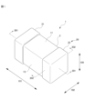
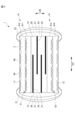
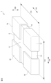
- FIG. 1 is a perspective view of a multilayer ceramic capacitor according to an embodiment of the present invention; This is a cross-sectional view taken along line 201-201 in Figure 1. This is a cross-sectional view taken along line 202-202 in Figure 1. This is a cross-sectional view corresponding to the line 201-201 in FIG. This is a cross-sectional view corresponding to the line 201-201 in FIG.
- FIG. 2 is a perspective view of another multilayer ceramic capacitor according to the present embodiment.
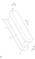
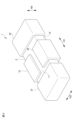
- 1 is a perspective view of a multilayer ceramic capacitor according to an embodiment of the present invention; 1 is a perspective view of a multilayer ceramic capacitor according to an embodiment of the present invention; 1 is a perspective view of a multilayer ceramic capacitor according to an embodiment of the present invention;
- Fig. 1 is a perspective view of the multilayer ceramic capacitor 1 of the present embodiment.
- the multilayer ceramic capacitor 1 includes a laminate 2 and external electrodes 20.
- the external electrodes 20 include a first external electrode 21 and a second external electrode 22.
- Fig. 2 is a cross-sectional view taken along line 201-201 in Fig. 1.
- the laminate 2 includes a plurality of stacked internal electrodes 30 and a plurality of stacked dielectric layers 40.
- the direction in which the internal electrodes 30 and the dielectric layers 40 are stacked is referred to as the stacking direction 100.
- the shape of the laminate 2 is approximately a rectangular parallelepiped.
- the surfaces of the laminate 2 are called as follows.
- the two surfaces facing the stacking direction 100 are called a first surface 11 and a second surface 12.
- the two surfaces facing a first direction 101 perpendicular to the stacking direction 100 are called a third surface 13 and a fourth surface 14.
- the two surfaces facing a second direction 102 perpendicular to the stacking direction 100 and the first direction 101 are called a fifth surface 15 and a sixth surface 16.
- the preferred surface condition of the first surface 11 and the second surface 12, or the preferred surface condition of one of the first surface 11 and the second surface 12, is flat.
- the multilayer ceramic capacitor 1 When the multilayer ceramic capacitor 1 is picked up, it is subjected to stress from the pick-up nozzle.
- the flat surface of the laminate disperses this stress across the flat surface.
- the surface of the laminate 2 may be roughened.
- a portion where two of the first surface 11, the second surface 12, the third surface 13, the fourth surface 14, the fifth surface 15, and the sixth surface 16 intersect is called a ridge portion.
- a portion where three of the first surface 11, the second surface 12, the third surface 13, the fourth surface 14, the fifth surface 15, and the sixth surface 16 intersect is called a corner portion.
- the preferred shape of the ridges and corners is rounded. Rounded ridges and corners prevent the laminate 2 from chipping and cracking.
- the surface of the laminate 2 excluding the corners and ridges may be flat.
- the laminate 2 has an inner layer portion 53 and an outer layer portion 50.
- the inner layer portion 53 is a portion where the internal electrodes 30 and the dielectric layers 40 are laminated.
- the outer layer portion 50 is a portion where the dielectric layers 40 are laminated.
- the outer layer portion 50 includes a first surface side outer layer portion 51 and a second surface side outer layer portion 52.
- the first surface side outer layer portion 51 is an outer layer portion 50 located between the inner layer portion 53 and the first surface 11.
- the second surface side outer layer portion 52 is an outer layer portion 50 located between the inner layer portion 53 and the second surface 12.
- the outer layer portion 50 sandwiches the inner layer portion 53 in the stacking direction 100 between the first surface side outer layer portion 51 and the second surface side outer layer portion 52.
- the layer structure of the inner layer 53 and the outer layer 50 will be described.
- the inner electrode 30 includes a first inner electrode 31 and a second inner electrode 32.
- the dielectric layer 40 includes an outer dielectric layer 41 and an inner dielectric layer 43.
- the inner layer portion 53 includes a first inner electrode 31, a second inner electrode 32, and an inner-layer dielectric layer 43.
- the first inner electrode 31 is an inner electrode 30 having one end exposed on the third surface 13.
- the second inner electrode 32 is an inner electrode 30 having one end exposed on the fourth surface 14.
- the inner-layer dielectric layer 43 is a dielectric layer 40 that is alternately laminated with the first inner electrode 31 and the second inner electrode 32.
- the inner dielectric layer 43 includes a first region 45 and a second region 46.
- An end of the inner electrode 30 in the first direction 101 that is not exposed to the third face or the fourth face is called the inner electrode end 34.
- the first region 45 is a region of the inner dielectric layer 43 that covers the inner electrode end 34.
- the surface of the internal electrode 30 in the lamination direction 100 is called the lamination direction surface 35.
- the second region 46 is a region of the inner dielectric layer 43 that covers the lamination direction surface 35.
- the dielectric component contained most abundantly in the first region 45 and the dielectric component contained most abundantly in the second region 46 are of the same type.
- the dielectric component is not limited.
- the dielectric component contains a large amount of calcium titanate or calcium zirconate, the following effects can be obtained: It is possible to suppress the occurrence of dielectric breakdown between the internal electrode end 34 of the first internal electrode 31 and the second external electrode 22, the occurrence of dielectric breakdown between the internal electrode end 34 of the second internal electrode 32 and the first external electrode 21, and the occurrence of dielectric breakdown between the first internal electrode 31 and the second internal electrode 32.
- the dielectric component is not limited to calcium titanate or calcium zirconate.
- the main component of the dielectric component may be strontium titanate.
- the main component of the dielectric component may be barium titanate.
- Barium titanate has a high dielectric constant.
- the capacitance of the multilayer ceramic capacitor 1 becomes high.
- the internal electrode 30 includes a facing region 37 and an extended region 38.
- the facing region 37 is a region where the first internal electrode 31 and the second internal electrode 32 face each other.
- the extended region 38 is a region extended from the facing region 37 onto the third surface 13, and a region extended from the facing region 37 onto the fourth surface 14.
- the width of the internal electrode 30 in the second direction 102 may vary toward one end exposed on the third surface 13 or the fourth surface 14.
- Examples of the components of the internal electrodes 30 include metals such as nickel, copper, silver, palladium, and gold, as well as alloys containing at least one of the above-mentioned metals, such as a silver-palladium alloy.
- the components of the internal electrodes 30 are not particularly limited as long as they are conductive materials.
- the internal electrodes 30 may contain tin.
- the electric field concentration at the interface between the internal electrodes 30 and the dielectric layers 40 is alleviated. As a result, the high temperature load reliability of the multilayer ceramic capacitor 1 is improved.
- Tin may be contained in either the first internal electrode 31 or the second internal electrode 32.
- tin in either the first internal electrode 31 or the second internal electrode 32, electric field concentration is alleviated and high temperature load reliability is improved.
- Fig. 3 is a cross-sectional view taken along line 202-202 in Fig. 1.
- the region between the first internal electrode 31 and the fifth surface 15, and the region between the second internal electrode 32 and the fifth surface 15 are referred to as a first width direction region 55.
- the region between the first internal electrode 31 and the sixth surface 16, and the region between the second internal electrode 32 and the sixth surface 16 are referred to as a second width direction region 56.
- Silicon may be segregated between the internal electrode 30 and the first widthwise region 55, or between the internal electrode 30 and the second widthwise region 56.
- the segregated silicon improves the flexural strength of the multilayer ceramic capacitor 1.
- the first surface side outer layer portion 51 and the second surface side outer layer portion 52 are formed of an insulating material.
- the first surface side outer layer portion 51 and the second surface side outer layer portion 52 are formed of the same type of dielectric material as the inner dielectric layer 43, the first surface side outer layer portion 51 and the second surface side outer layer portion 52 may be composed of a plurality of outer dielectric layers 41 or may be composed of a single outer dielectric layer 41.
- the inner dielectric layer 43 and the outer dielectric layer 41 may be formed from different components.
- the components of the inner dielectric layer 43 may have a higher dielectric constant than the components of the outer dielectric layer 41.
- the components of the outer dielectric layer 41 may be components with good moisture resistance, weather resistance, or strength resistance.
- the external electrode 20 will be described. As shown in Fig. 2, the external electrode 20 has a first external electrode 21 and a second external electrode 22. The first external electrode 21 is the external electrode 20 disposed on the third surface 13. The second external electrode 22 is the external electrode 20 disposed on the fourth surface 14.
- the external electrode 20 is arranged so as to extend around the first surface 11, the second surface 12, the fifth surface 15 and the sixth surface 16.
- the external electrode 20 includes a base electrode layer 24 and a plating layer 26.
- the base electrode layer 24 and the plating layer 26 are disposed in this order from the laminate 2 side.
- the base electrode layer 24 is preferably made of a metal such as copper or nickel.
- the base electrode layer 24 may contain the same dielectric component as the main component of the inner dielectric layer 43.
- the difference in thermal expansion coefficient between the laminate 2 and the base electrode layer 24 is reduced. As a result, the stress applied to the base electrode layer 24 is alleviated.
- the base electrode layer 24 may contain metals other than copper and nickel as metal components. Examples of other metal components are magnesium, chromium, strontium, aluminum, sodium, and iron.
- the base electrode layer 24 may contain a glass component in addition to the dielectric component.
- the glass component are oxides of barium, strontium, silicon, calcium, zinc, aluminum, or boron.
- a metal layer may be disposed in place of the base electrode layer 24.
- the metal layer may be disposed on both the first surface 11 and the second surface 12, or on either the first surface 11 or the second surface 12.
- a plated electrode may be formed to connect to the internal electrode 30 and the metal film.
- the thickness of the metal film can be reduced to 1 ⁇ m or less. This allows the dimensions of the multilayer ceramic capacitor 1 in the stacking direction 100 to be reduced.
- the plating layer 26 is disposed on the base electrode layer 24.
- the plating layer 26 preferably has at least a two-layer structure.
- An example of the two layers is a nickel plating layer 27 and a tin plating layer 28.
- Figures 2 and 3 show a configuration in which the plating layer 26 includes the nickel plating layer 27 and the tin plating layer 28.
- the nickel plating layer 27 and the tin plating layer 28 are disposed in this order from the base electrode layer 24 side: the nickel plating layer 27, the tin plating layer 28.
- the nickel plating layer 27 prevents the base electrode layer 24 from being corroded by the solder.
- the tin plating layer 28 improves the mountability of the multilayer ceramic capacitor 1 on a substrate, etc.
- the plating layer 26 may include three or more layers.
- the layers may be arranged in the following order from the base electrode layer 24 side: a tin plating layer, a nickel plating layer, and a tin plating layer.
- the plating layer 26 preferably contains at least one metal selected from, for example, copper, nickel, tin, lead, gold, silver, palladium, bismuth, and zinc, or an alloy containing these metals.
- the plating layer preferably does not contain glass.
- the metal ratio per unit volume of the plating layer is preferably 99 volume % or more.
- Fig. 4 is a view corresponding to the cross-sectional view taken along line 201-201 in Fig. 1.
- the multilayer ceramic capacitor 1 has fibers 60 in the laminate 2. Examples of the fibers 60 include carbon or silicon carbide fibers, alumina fibers, and boron fibers.
- Having fibers 60 in the laminate 2 means having fibers 60 in any one of the internal electrode 30, the inner dielectric layer 43, and the outer dielectric layer 41, or having fibers 60 in only one of them.
- the first face side outer layer 51 and the second face side outer layer 52 have fibers 60. However, at least one of the first face side outer layer 51 and the second face side outer layer 52 may have fibers 60.
- the fibers 60 may be intertwined with one another. By intertwining the fibers 60 with one another, the mechanical strength of the multilayer ceramic capacitor 1 is further improved.
- each of the layers may have fibers 60, or each layer may have a layer having fibers 60 and a layer not having fibers 60 laminated together.
- an outer dielectric layer 41 having fibers 60 and an outer dielectric layer 41 not having fibers 60 may be prepared and laminated together.
- the fibers 60 can be prevented from being exposed on the surface of the laminate 2.
- FIG. 5 is a diagram equivalent to the cross-sectional view taken along line 201-201 in FIG. 1.
- the first surface side outer layer portion 51 and the second surface side outer layer portion 52 each include one outer dielectric layer 41.
- the first surface side outer layer portion 51 and the second surface side outer layer portion 52 each include two outer dielectric layers 41.
- the two outer dielectric layers 41 included in the first surface side outer layer portion 51 are shown as outer dielectric layer 411 and outer dielectric layer 412.
- the two outer dielectric layers 41 included in the second surface side outer layer portion 52 are shown as outer dielectric layer 413 and outer dielectric layer 414.
- the outer dielectric layer 411, the outer dielectric layer 412, the outer dielectric layer 413, and the outer dielectric layer 414 each have fibers 60. Therefore, multiple layers of entangled fibers 60 are formed in the first surface side outer layer portion 51 and the second surface side outer layer portion 52. As a result, the mechanical strength of the multilayer ceramic capacitor 1 is further improved.
- each fiber 60 is too thick or too large, the fibers 60 will not entangle with each other and will be scattered. In this case, the mechanical strength of the multilayer ceramic capacitor 1 will not improve. In addition, there is a risk of cracks occurring inside the laminate 2 due to the difference in shrinkage between the fibers 60 and the dielectric component during firing, which will be described later.
- the aspect ratio of the fibers 60 (length of the fibers 60/thickness of the fibers 60) is small, the fibers 60 will not entangle with each other, and the mechanical strength of the multilayer ceramic capacitor 1 will not improve.
- each fiber 60 is 1 ⁇ m or more and 100 ⁇ m or less. If each fiber 60 is too long, the fiber 60 itself becomes tangled and tends to aggregate. It is also preferable that the thickness of each fiber 60 is 1 nm or more and 1000 nm or less. It is preferable that the number of intersections between the fibers 60 is 5 or more in an area of 2.5 ⁇ m x 2.5 ⁇ m or less. This causes the fibers 60 to become entangled, improving the mechanical strength of the multilayer ceramic capacitor 1.
- Relatively long fibers 60 are, for example, fibers 60 with a length of 1 ⁇ m or more to 100 ⁇ m.
- the desired amount is, for example, an amount in which "5 or more fibers 60 are found in an area of 2.5 ⁇ m x 2.5 ⁇ m or less" in the multilayer ceramic capacitor 1 after sintering.
- the thickness of the fibers 60 is polished to 1/2 the dimension of the multilayer ceramic capacitor 1 in the second direction 102, exposing a cross section parallel to the stacking direction 100 and the first direction 101 of the multilayer ceramic capacitor 1.
- each fiber 60 is observed within an observation field of view of 2.5 ⁇ m x 2.5 ⁇ m, within a range in which at least 10 fibers can be observed, more specifically, within an observation field of view of 250 nm x 250 nm, or within a range in which 2.5 ⁇ m x 2.5 ⁇ m can be observed.
- the number of intersections between fibers 60 can be determined by counting the number of intersections between fibers 60 in an observation field of view of 2.5 ⁇ m x 2.5 ⁇ m. Specifically, when fibers 60 are viewed as lines, the number of intersections is the number of points at which fibers 60 as one line intersect with fibers 60 as another line.
- the content of the fibers 60 will be described.
- the content of the fibers 60 is preferably 1.0 wt% or more and 30.0 wt% or less.
- the content of the fibers 60 is preferably 1.0 wt% or more and 30.0 wt% or less.
- the content of the fibers 60 is preferably 1.0 wt% or more and 30.0 wt% or less.
- the content of the fibers 60 is 1.0 wt% or more and 30.0 wt% or less.
- the content of the fibers 60 is too low, the total amount of the fibers 60 is small, making it difficult to improve the mechanical strength.
- the content of fiber 60 can be determined by the amount of fiber 60 added during the manufacture of the multilayer ceramic capacitor 1.
- the content of fibers 60 is defined and confirmed as follows.
- the multilayer ceramic capacitor 1 is polished to 1/2 of its dimension in the second direction 102 to expose a cross section parallel to the lamination direction 100 and first direction 101 of the multilayer ceramic capacitor 1.
- the cross section thus obtained is divided into 5 equal parts in the first direction 101, and the central 5 regions of each region are observed using a scanning probe microscope with an observation field of view of 2.5 ⁇ m x 2.5 ⁇ m. Each observation image is binarized, and the content is defined as the average of the values in the 5 regions.
- the dimensions of the multilayer ceramic capacitor 1 will now be described.
- the dimensions of the multilayer ceramic capacitor 1 including the external electrodes 20 are not particularly limited.
- the dimension of the multilayer ceramic capacitor 1 in the lamination direction 100 becomes small, the mechanical strength of the multilayer ceramic capacitor 1 in the lamination direction 100 decreases. Therefore, when the dimension of the multilayer ceramic capacitor 1 in the lamination direction 100 is, for example, 110 ⁇ m or less, applying the configuration of this embodiment to the multilayer ceramic capacitor 1 improves the mechanical strength of the multilayer ceramic capacitor 1 in the lamination direction 100 in particular.
- the dimension of the multilayer ceramic capacitor 1 in the stacking direction 100 is preferably 80 ⁇ m or less, more preferably 60 ⁇ m or less, and even more preferably 40 ⁇ m or less. If it is 80 ⁇ m or less, the mechanical strength in the stacking direction 100 will be significantly weakened, so the configuration of the present application can be more effectively demonstrated.
- Step 1 a dielectric sheet for the inner dielectric layer 43 and a conductive paste for the internal electrode 30 are prepared.
- the dielectric sheet, the conductive paste for the internal electrode 30, and the dielectric sheet contain a binder and an organic solvent. Known materials can be used for the binder and the organic solvent.
- a dielectric paste for the first region 45 of the inner dielectric layer 43 may be prepared separately.
- the dielectric material for the first region 45 and the second region may be changed to calcium zirconate, barium titanate, or the like. Note that the dielectric material is not limited to these and may be any desired material.
- fiber 60 is added separately. At this time, the content of fiber 60 can be changed by changing the amount of fiber 60 added. Also, if the materials are not sufficiently dispersed, fiber 60 may clump together. For this reason, it is preferable to thoroughly disperse each material, including fiber 60. If the outer dielectric layer 41 has a layered structure, for example, by including fiber 60 near the center in the stacking direction, fiber 60 may be distributed in layers due to the dispersion of fiber 60.
- the fibers 60 are on the first surface 11 or the second surface 12 of the outer dielectric layer 41, which has a layered structure, it is possible to prevent cracks from occurring in the multilayer ceramic capacitor 1 due to the impact of the mounter during mounting.
- the fibers 60 are located on the internal electrode 30 side of the outer dielectric layer 41, which has a layered structure, even if a crack occurs on the first surface 11 or the second surface 12, the crack can be prevented from spreading to the layer of the internal electrode 30.
- Step 2 a conductive paste for the internal electrodes 30 is printed in a predetermined pattern on the dielectric sheet. This forms a dielectric sheet on which the internal electrode pattern of the inner layer portion 53 is printed.
- the printing of the conductive paste for the internal electrodes 30 on the dielectric sheet is performed by, for example, screen printing or gravure printing.
- Step 3 the dielectric sheet and the dielectric sheet on which the internal electrode pattern is printed are laminated.
- the laminated dielectric sheets are pressed in the lamination direction 100 by, for example, an isostatic press. As a result, a laminated block is formed.
- Step 4 the laminated block is cut to a predetermined size, thereby cutting out laminated chips. After this, corners and edges of the laminated chips may be rounded by barrel polishing or the like.
- step 5 the laminated chip is fired to form the laminated body 2 according to this embodiment.
- Step 6 a conductive paste containing a glass component and a metal component is applied to the third surface 13 and the fourth surface 14 by, for example, a dipping method, thereby forming a base electrode layer 24.
- a conductive paste may be applied to the fifth surface 15 and the sixth surface 16 by extruding the conductive paste from a slit plate, and then the conductive paste may be applied to the third surface 13 and the fourth surface 14 by, for example, a dipping method.
- the base electrode layer 24 can also be formed in this way.
- Step 7 a plating layer 26 is formed so as to be connected to the base electrode layer 24.
- electrolytic plating is preferably used.
- barrel plating is preferably used.
- FIG. 6 is a diagram showing an outline of the multilayer ceramic capacitor 1 of the thin product.
- the length 110 in the stacking direction 100 of the multilayer ceramic capacitor 1 shown in FIG. 6 is shorter than the length 112 in the second direction 102 of the multilayer ceramic capacitor 1. In this way, the multilayer ceramic capacitor 1 in which the length 110 is shorter than the length 112 is called a thin product.
- the thin product is likely to be insufficient in strength compared to the multilayer ceramic capacitor 1 in which the length 110 and the length 112 are almost equal as shown in FIG. 1.
- the laminate 2 has the fibers 60. Therefore, the strength of the thin multilayer ceramic capacitor 1 can be increased.
- FIG. 7 is a diagram showing an overview of a multilayer ceramic capacitor 1 in which the external electrodes 20 are arranged in the lateral direction of the multilayer ceramic capacitor 1.
- the external electrodes 20 are arranged not on the longitudinal end faces, i.e., the third face 13 and the fourth face 14, but on the lateral end faces, i.e., the fifth face 15 and the sixth face 16.
- the external electrode 72 is arranged on the fifth face 15, and the external electrode 71 is arranged on the sixth face 16.
- the external electrodes 20 may be arranged in the lateral direction of the multilayer ceramic capacitor 1 of this embodiment.
- FIG. 8 is a diagram showing a multilayer ceramic capacitor 1 having three terminals. As shown in FIG. 8, the multilayer ceramic capacitor 1 of this embodiment may have external electrodes 74 and 75 as a third terminal in addition to the first external electrode 21 and the second external electrode 22.
- the multilayer ceramic capacitor 1 of this embodiment may have the same length in the first direction 101 and the same length in the second direction 102.
- FIG. 9 is a diagram showing a so-called square-type multilayer ceramic capacitor 1. As shown in FIG. 9, the multilayer ceramic capacitor 1 may have the same length 114 in the first direction 101 and the same length 116 in the second direction 102. A multilayer ceramic capacitor 1 in which the length 114 in the first direction 101 and the length 116 in the second direction 102 are equal is called a square-type multilayer ceramic capacitor 1.
- external electrodes 20 may be arranged at the four corners of a plane parallel to the first direction 101 and the second direction 102.
- external electrodes 77, 78, 79, and 80 are arranged as external electrodes 20.
- a laminate having a first surface and a second surface opposed to each other in a stacking direction, a third surface and a fourth surface opposed to each other in a first direction perpendicular to the stacking direction, and a fifth surface and a sixth surface opposed to each other in a second direction perpendicular to the stacking direction and the first direction; a first external electrode disposed on a third surface of the laminate; a second external electrode disposed on a fourth surface of the laminate; Equipped with The laminate comprises: The inner layer and Two outer layer portions arranged to sandwich the inner layer portion in the stacking direction; Equipped with The outer layer portion includes an outer dielectric layer, The outer dielectric layer contains fibers. Multilayer ceramic capacitor.
- the thickness of the fiber is 1 nm or more and 1000 nm or less
- the content of the fiber is 1.0 wt% or more and 30.0 wt% or less
- ⁇ 1> The multilayer ceramic capacitor according to any one of ⁇ 1> to ⁇ 3>.
- ⁇ 5> The number of intersections between the fibers is 5 or more in a 2.5 ⁇ m ⁇ 2.5 ⁇ m region in a cross section parallel to the lamination direction and the first direction, ⁇ 4>
- ⁇ 6> The dimension in the lamination direction is 80 ⁇ m or less
- ⁇ 5> The multilayer ceramic capacitor according to any one of ⁇ 1> to ⁇ 5>.
Landscapes
- Engineering & Computer Science (AREA)
- Power Engineering (AREA)
- Manufacturing & Machinery (AREA)
- Microelectronics & Electronic Packaging (AREA)
- Ceramic Capacitors (AREA)
- Fixed Capacitors And Capacitor Manufacturing Machines (AREA)
Abstract
強度を十分に確保できる積層セラミックコンデンサを提供すること。積層セラミックコンデンサ(1)は、第1の面(11)から第6の面(16)の6つの面を含む積層体(2)と、第1の外部電極(21)と、第2の外部電極(22)と、を備え、積層体(2)は、内層部(53)と、内層部(53)を積層方向(100)に挟み込むように配置された2つの外層部(50)と、を備え、外層部(50)は、外層誘電体層(41)を備え、外層誘電体層(41)中に、繊維(60)を含有している。
Description
本発明は、積層セラミックコンデンサに関する。
近年、携帯電話機や携帯音楽プレイヤーなどの電子機器の小型化や薄型化が進んでいる。電子機器には、多数の積層セラミック電子部品が搭載されているが、電子機器の小型化に伴って、基板に内蔵されたり、基板表面に実装されたりして電子機器に搭載される積層セラミック電子部品についても、例えば特許文献1などに記載の積層セラミックコンデンサのような、第1端面の法線方向に垂直かつ第1内部電極に垂直な方向の外形寸法をTとしたときに、T≦100μmの積層セラミックコンデンサなど、小型化や薄型化が進んできている。このような積層セラミックコンデンサの小型化や薄型化に伴い、積層セラミックコンデンサの強度の確保が課題となってきている。
そこで、本願は、強度を十分に確保できる積層セラミックコンデンサを提供することを目的とする。
本発明の積層セラミックコンデンサは、積層方向に相対する第1の面および第2の面と、前記積層方向に直交する第1の方向に相対する第3の面および第4の面と、前記積層方向および前記第1の方向に直交する第2の方向に相対する第5の面と第6の面とを有する積層体と、前記積層体の第3の面上に配置された第1の外部電極と、前記積層体の第4の面上に配置された第2の外部電極と、を備え、前記積層体は、内層部と、前記内層部を前記積層方向に挟み込むように配置された2つの外層部と、を備え、前記外層部は、外層誘電体層を備え、前記外層誘電体層中に、繊維を含有している。
本発明によれば、強度を十分に確保できる積層セラミックコンデンサを提供することができる。
(積層セラミックコンデンサ)
図1を参照して、積層セラミックコンデンサ1の概要を説明する。図1は、本実施形態の積層セラミックコンデンサ1の斜視図である。積層セラミックコンデンサ1は、積層体2および外部電極20を含む。外部電極20は、第1の外部電極21および第2の外部電極22を含む。
図1を参照して、積層セラミックコンデンサ1の概要を説明する。図1は、本実施形態の積層セラミックコンデンサ1の斜視図である。積層セラミックコンデンサ1は、積層体2および外部電極20を含む。外部電極20は、第1の外部電極21および第2の外部電極22を含む。
(積層体)
図2を参照して、積層体2の内部構造を説明する。図2は、図1の201-201線断面図である。積層体2は、積層された、複数の内部電極30および複数の誘電体層40を含む。内部電極30と誘電体層40が積層される方向を、積層方向100と呼ぶ。
図2を参照して、積層体2の内部構造を説明する。図2は、図1の201-201線断面図である。積層体2は、積層された、複数の内部電極30および複数の誘電体層40を含む。内部電極30と誘電体層40が積層される方向を、積層方向100と呼ぶ。
(積層体の面)
図1に示すように、積層体2の形状は、およそ直方体形状である。積層体2の各面をつぎのように呼ぶ。積層方向100に相対する2つの面を、第1の面11および第2の面12と呼ぶ。積層方向100に直交する第1の方向101に相対する2つの面を、第3の面13および第4の面14と呼ぶ。積層方向100および第1の方向101に直交する第2の方向102に相対する2つの面を、第5の面15および第6の面16と呼ぶ。
図1に示すように、積層体2の形状は、およそ直方体形状である。積層体2の各面をつぎのように呼ぶ。積層方向100に相対する2つの面を、第1の面11および第2の面12と呼ぶ。積層方向100に直交する第1の方向101に相対する2つの面を、第3の面13および第4の面14と呼ぶ。積層方向100および第1の方向101に直交する第2の方向102に相対する2つの面を、第5の面15および第6の面16と呼ぶ。
第1の面11および第2の面12の好ましい表面状態、または、第1の面11および第2の面12のうちの一方の面の好ましい表面状態は、平坦である。
積層セラミックコンデンサ1は、ピックアップされる際、ピックアップ用のノズルから応力を受ける。積層体の平坦な面は、この応力を、その平坦な面で分散させる。なお、積層体2の表面は粗されていてもよい。
(稜線部および角部)
第1の面11、第2の面12、第3の面13、第4の面14、第5の面15および第6の面16のうち、二面が交わる部分を稜線部と呼ぶ。第1の面11、第2の面12、第3の面13、第4の面14、第5の面15および第6の面16のうち、三面が交わる部分を角部と呼ぶ。
第1の面11、第2の面12、第3の面13、第4の面14、第5の面15および第6の面16のうち、二面が交わる部分を稜線部と呼ぶ。第1の面11、第2の面12、第3の面13、第4の面14、第5の面15および第6の面16のうち、三面が交わる部分を角部と呼ぶ。
稜線部および角部の好ましい形状は、丸みを有する形状である。丸みを有する稜線部および角部は、積層体2がかけること、および積層体が割れることを抑制する。
稜線部および角部が丸みを有する場合、角部および稜線部を除く積層体2の面は、平坦であってもよい。
(内層部および外層部)
図2に示すように、積層体2は、内層部53および外層部50を有する。内層部53は、内部電極30および誘電体層40が積層された部分である。外層部50は、誘電体層40が積層された部分である。
図2に示すように、積層体2は、内層部53および外層部50を有する。内層部53は、内部電極30および誘電体層40が積層された部分である。外層部50は、誘電体層40が積層された部分である。
外層部50は、第1の面側外層部51および第2の面側外層部52を含む。第1の面側外層部51は、内層部53と第1の面11との間に位置する外層部50である。第2の面側外層部52は、内層部53と第2の面12との間に位置する外層部50である。外層部50は、第1の面側外層部51および第2の面側外層部52によって、内層部53を積層方向100に挟み込む。
内層部53および外層部50の層構成を説明する。内部電極30は、第1の内部電極31および第2の内部電極32を含む。誘電体層40は、外層誘電体層41および内層誘電体層43を含む。
(内層部)
内層部53は、第1の内部電極31、第2の内部電極32および内層誘電体層43を含む。第1の内部電極31は、第3の面13上に一端が露出される内部電極30である。第2の内部電極32は、第4の面14上に一端が露出される内部電極30である。内層誘電体層43は、第1の内部電極31および第2の内部電極32と交互に積層される誘電体層40である。
内層部53は、第1の内部電極31、第2の内部電極32および内層誘電体層43を含む。第1の内部電極31は、第3の面13上に一端が露出される内部電極30である。第2の内部電極32は、第4の面14上に一端が露出される内部電極30である。内層誘電体層43は、第1の内部電極31および第2の内部電極32と交互に積層される誘電体層40である。
(第1の領域および第2の領域)
内層誘電体層43は、第1の領域45および第2の領域46を含む。内部電極30の、第3の面または第4の面に露出されない第1の方向101における一端を、内部電極端34と呼ぶ。第1の領域45は、内層誘電体層43において、内部電極端34を被覆する領域である。
内層誘電体層43は、第1の領域45および第2の領域46を含む。内部電極30の、第3の面または第4の面に露出されない第1の方向101における一端を、内部電極端34と呼ぶ。第1の領域45は、内層誘電体層43において、内部電極端34を被覆する領域である。
内部電極30の、積層方向100の表面を、積層方向表面35と呼ぶ。第2の領域46は、内層誘電体層43において、積層方向表面35を被覆する領域である。
第1の領域45が最も多く含む誘電体成分と、第2の領域46が最も多く含む誘電体成分とは、同種であることが好ましい。なお、誘電体成分は、限定されない。
誘電体成分が、チタン酸カルシウムまたはジルコン酸カルシウムを多く含む場合、つぎの効果が得られる。第1の内部電極31の内部電極端34と第2の外部電極22との間での絶縁破壊の発生、第2の内部電極32の内部電極端34と第1の外部電極21との間での絶縁破壊の発生、および第1の内部電極31と第2の内部電極32との間での絶縁破壊の発生を抑制できる。
誘電体成分は、チタン酸カルシウムまたはジルコン酸カルシウムに限定されない。誘電体成分の主成分は、チタン酸ストロンチウムであってもよい。
誘電体成分の主成分は、チタン酸バリウムであってもよい。チタン酸バリウムの誘電率は高い。誘電体成分の主成分がチタン酸バリウムである場合、積層セラミックコンデンサ1の容量は、高くなる。
(対向領域および引き出し領域)
内部電極30は、対向領域37および引き出し領域38を含む。対向領域37は、第1の内部電極31と第2の内部電極32とが対向する領域である。引き出し領域38は、対向領域37から第3の面13上に引き出される領域、および対向領域37から第4の面14上に引き出される領域である。
内部電極30は、対向領域37および引き出し領域38を含む。対向領域37は、第1の内部電極31と第2の内部電極32とが対向する領域である。引き出し領域38は、対向領域37から第3の面13上に引き出される領域、および対向領域37から第4の面14上に引き出される領域である。
内部電極30の第2の方向102における幅は、第3の面13上または第4の面14上で露出される一端に向かって、変化してもよい。
(内部電極)
内部電極30の成分の例は、ニッケル、銅、銀、パラジウムおよび金などの金属、ならびに銀-パラジウム合金などの、前述の金属の少なくとも一種を含む合金である。内部電極30の成分は、導電材料であれば、特に限定されない。
内部電極30の成分の例は、ニッケル、銅、銀、パラジウムおよび金などの金属、ならびに銀-パラジウム合金などの、前述の金属の少なくとも一種を含む合金である。内部電極30の成分は、導電材料であれば、特に限定されない。
(スズの含有)
内部電極30は、スズを含んでもよい。内部電極30がスズを含む場合、内部電極30と誘電体層40との界面への電界集中が緩和される。その結果、積層セラミックコンデンサ1の高温負荷信頼性が向上する。
内部電極30は、スズを含んでもよい。内部電極30がスズを含む場合、内部電極30と誘電体層40との界面への電界集中が緩和される。その結果、積層セラミックコンデンサ1の高温負荷信頼性が向上する。
スズは、第1の内部電極31および第2の内部電極32のうちのいずれか一方に含まれてもよい。第1の内部電極31および第2の内部電極32のうちのいずれか一方にスズが含まれることによって、電界集中が緩和し、高温負荷信頼性が向上する。
(第1の幅方向領域および第2の幅方向領域)
図3を参照して、積層体2の第2の方向102の構成を説明する。図3は、図1の202-202線断面図である。第1の内部電極31と第5の面15との間の領域、および第2の内部電極32と第5の面15との間の領域を、第1の幅方向領域55と呼ぶ。第1の内部電極31と第6の面16との間の領域、および第2の内部電極32と第6の面16との間の領域を、第2の幅方向領域56と呼ぶ。
図3を参照して、積層体2の第2の方向102の構成を説明する。図3は、図1の202-202線断面図である。第1の内部電極31と第5の面15との間の領域、および第2の内部電極32と第5の面15との間の領域を、第1の幅方向領域55と呼ぶ。第1の内部電極31と第6の面16との間の領域、および第2の内部電極32と第6の面16との間の領域を、第2の幅方向領域56と呼ぶ。
(ケイ素の偏析)
内部電極30と第1の幅方向領域55との間、または内部電極30と第2の幅方向領域56との間に、ケイ素が偏析してもよい。偏析したケイ素は、積層セラミックコンデンサ1の抗折強度を向上させる。
内部電極30と第1の幅方向領域55との間、または内部電極30と第2の幅方向領域56との間に、ケイ素が偏析してもよい。偏析したケイ素は、積層セラミックコンデンサ1の抗折強度を向上させる。
(第1の面側外層部および第2の面側外層部)
第1の面側外層部51および第2の面側外層部52は、絶縁性の材料によって形成される。第1の面側外層部51および第2の面側外層部52が、内層誘電体層43と同種の誘電体材料によって形成される場合、第1の面側外層部51および第2の面側外層部52は、複数の外層誘電体層41から成っていてもよく、または単数の外層誘電体層41から成っていてもよい。
第1の面側外層部51および第2の面側外層部52は、絶縁性の材料によって形成される。第1の面側外層部51および第2の面側外層部52が、内層誘電体層43と同種の誘電体材料によって形成される場合、第1の面側外層部51および第2の面側外層部52は、複数の外層誘電体層41から成っていてもよく、または単数の外層誘電体層41から成っていてもよい。
内層誘電体層43と外層誘電体層41とを異なる成分で形成することも可能である。例えば、内層誘電体層43の成分を、外層誘電体層41の成分よりも誘電率の高い成分としてもよい。
外層誘電体層41の成分を、耐湿性、耐候性または耐強度性のよい成分にしてもよい。
(外部電極)
外部電極20を説明する。図2に示すように外部電極20は、第1の外部電極21および第2の外部電極22を有する。第1の外部電極21は、第3の面13上に配置される外部電極20である。第2の外部電極22は、第4の面14上に配置される外部電極20である。
外部電極20を説明する。図2に示すように外部電極20は、第1の外部電極21および第2の外部電極22を有する。第1の外部電極21は、第3の面13上に配置される外部電極20である。第2の外部電極22は、第4の面14上に配置される外部電極20である。
外部電極20は、第1の面11、第2の面12、第5の面15および第6の面16にまで回り込んで配置されることが好ましい。
(下地電極層およびめっき層)
外部電極20は、下地電極層24およびめっき層26を含む。下地電極層24およびめっき層26は、積層体2の側から順に、下地電極層24およびめっき層26の順で配置される。
外部電極20は、下地電極層24およびめっき層26を含む。下地電極層24およびめっき層26は、積層体2の側から順に、下地電極層24およびめっき層26の順で配置される。
(下地電極層)
下地電極層24は、銅やニッケルなどの金属からなることが好ましい。下地電極層24は、金属成分に加えて、内層誘電体層43の主成分と同じ誘電体成分を含んでもよい。下地電極層24が内層誘電体層43の主成分と同じ誘電体成分を含む場合、積層体2と下地電極層24との間の熱膨張率の差が低減される。その結果、下地電極層24にかかる応力が緩和される。
下地電極層24は、銅やニッケルなどの金属からなることが好ましい。下地電極層24は、金属成分に加えて、内層誘電体層43の主成分と同じ誘電体成分を含んでもよい。下地電極層24が内層誘電体層43の主成分と同じ誘電体成分を含む場合、積層体2と下地電極層24との間の熱膨張率の差が低減される。その結果、下地電極層24にかかる応力が緩和される。
なお、下地電極層24は、金属成分として、銅およびニッケル以外の金属を含んでもよい。他の金属成分の例は、マグネシウム、クロム、ストロンチウム、アルミニウム、ナトリウムおよび鉄である。
下地電極層24は、誘電体成分とは別にガラス成分を含んでもよい。ガラス成分の例は、バリウム、ストロンチウム、ケイ素、カルシウム、亜鉛、アルミニウムまたはホウ素などの酸化物である。
(金属膜)
下地電極層24にかわって、金属層が配置されてもよい。金属層は、第1の面11および第2の面12の両方、または、第1の面11および第2の面12のうちのどちらか一方に配置されてもよい。
下地電極層24にかわって、金属層が配置されてもよい。金属層は、第1の面11および第2の面12の両方、または、第1の面11および第2の面12のうちのどちらか一方に配置されてもよい。
金属膜が配置される場合、内部電極30および金属膜に接続されるように、めっき電極が形成されてもよい。
金属膜をスパッタリング法または蒸着法によって形成すると、金属膜の厚さを1μm以下にすることができる。そのため、積層セラミックコンデンサ1の積層方向100の寸法を小さくできる。
(めっき層)
めっき層26を説明する。めっき層26は、下地電極層24上に配置される。めっき層26は、少なくとも二層構造であることが好ましい。二層の例は、ニッケルめっき層27およびスズめっき層28である。図2および図3に、めっき層26がニッケルめっき層27およびスズめっき層28を含む構成を示す。ニッケルめっき層27およびスズめっき層28は、下地電極層24側から、ニッケルめっき層27、スズめっき層28の順で配置される。
めっき層26を説明する。めっき層26は、下地電極層24上に配置される。めっき層26は、少なくとも二層構造であることが好ましい。二層の例は、ニッケルめっき層27およびスズめっき層28である。図2および図3に、めっき層26がニッケルめっき層27およびスズめっき層28を含む構成を示す。ニッケルめっき層27およびスズめっき層28は、下地電極層24側から、ニッケルめっき層27、スズめっき層28の順で配置される。
ニッケルめっき層27は、下地電極層24がはんだによって侵食されることを防止する。スズめっき層28は、積層セラミックコンデンサ1の基板などへの実装性を向上させる。
めっき層26は、三層以上の層を含んでもよい。めっき層26が三層構造である場合、下地電極層24側から、スズめっき層、ニッケルめっき層、スズめっき層の順で配置されてもよい。
めっき層26は、例えば、銅、ニッケル、スズ、鉛、金、銀、パラジウム、ビスマスおよび亜鉛などから選ばれる少なくとも1種の金属、またはこれらの金属を含む合金を含むことが好ましい。めっき層は、ガラスを含まないことが好ましい。めっき層の単位体積あたりの金属割合は、99体積%以上であることが好ましい。
(繊維)
図4を参照して、繊維60を説明する。図4は、図1の201-201線断面図に相当する図である。積層セラミックコンデンサ1は、積層体2に、繊維60を有する。繊維60の例は、カーボンまたは炭化ケイ素の繊維、アルミナ繊維、ボロン繊維などである。
図4を参照して、繊維60を説明する。図4は、図1の201-201線断面図に相当する図である。積層セラミックコンデンサ1は、積層体2に、繊維60を有する。繊維60の例は、カーボンまたは炭化ケイ素の繊維、アルミナ繊維、ボロン繊維などである。
積層体2に繊維60を有するとは、内部電極30、内層誘電体層43および外層誘電体層41のうちのいずれかに繊維60を有すること、または、それらのうちのいずれかのみに繊維60を有すること、を意味する。
図4に示す例では、第1の面側外層部51および第2の面側外層部52が、繊維60を有する。ただし、第1の面側外層部51および第2の面側外層部52のうちの少なくとも一方のみが、繊維60を有してもよい。
第1の面側外層部51および第2の面側外層部52に繊維60を有することによって、積層セラミックコンデンサ1の誘電率および電気抵抗への影響が少なく、積層セラミックコンデンサ1の機械強度を向上させることができる。
繊維60は、複数の繊維60が絡みあっていてもよい。複数の繊維60が絡みあうことによって、積層セラミックコンデンサ1の機械強度は、より向上する。
第1の面側外層部51および第2の面側外層部52が複数の外層誘電体層41からなる場合、その一層一層が繊維60を有してもよく、または、各層で繊維60を有する層と繊維60を有さない層とが積層されてもよい。つまり、繊維60を有する外層誘電体層41と、繊維60を有さない外層誘電体層41とを準備し、それらが積層されてもよい。
ここで、繊維60を有さない外層誘電体層41が第1の面11および第2の面12に位置するように外層誘電体層41を配置することによって、繊維60が積層体2の表面に露出しないようにできる。
図5は、図1の201-201線断面図に相当する図である。図4に示す積層セラミックコンデンサ1は、第1の面側外層部51および第2の面側外層部52が、それぞれ、外層誘電体層41を一層ずつ含む。これに対して、図5に示す積層セラミックコンデンサ1は、第1の面側外層部51および第2の面側外層部52が、外層誘電体層41を二層ずつ含む。
図5において、第1の面側外層部51が含む二層の外層誘電体層41を外層誘電体層411および外層誘電体層412として示す。第2の面側外層部52が含む二層の外層誘電体層41を外層誘電体層413および外層誘電体層414として示す。
図5に示す例では、外層誘電体層411、外層誘電体層412、外層誘電体層413および外層誘電体層414が、それぞれ繊維60を有する。そのため、第1の面側外層部51および第2の面側外層部52に、繊維60の絡み合いが複数層形成される。その結果、積層セラミックコンデンサ1の機械強度は、より向上する。
繊維60一本の太さが太すぎる場合、または繊維60一本の大きさが大きすぎる場合、繊維60同士が互いに絡まず、繊維60が点在する状態となる。この場合、積層セラミックコンデンサ1の機械強度は向上しない。また、後述する焼成時に繊維60と誘電体成分との収縮差によって積層体2内部にクラックが発生する恐れがある。
また、繊維60のアスペクト比(繊維60の長さ/繊維60の太さ)が小さいと、繊維60同士が互いに絡まず、積層セラミックコンデンサ1の機械強度は、向上しない。
そこで、繊維60一本の長さは、1μm以上100μm以下であることが好ましい。繊維60一本の長さが長すぎると、繊維60自身が絡まって凝集しやすくなってしまう。また、繊維60一本の太さは、1nm以上1000nm以下であることが好ましい。繊維60同士の交錯数は、2.5μm×2.5μm以内の領域において5個以上であることが好ましい。これによって、繊維60の絡み合いが生じ、積層セラミックコンデンサ1の機械強度は、向上する。
繊維60同士の交錯数を2.5μm×2.5μm以内の領域において5個以上にするためには、例えば、比較的長い繊維60を所望の量だけ含有させることが考えられる。比較的長い繊維60とは、例えば、長さが1μm以上100μmの繊維60である。また、所望の量とは、例えば、焼結後の積層セラミックコンデンサ1において、繊維60が「2.5μm×2.5μm以内の領域において5個以上」見られる程度の量である。
繊維60の太さおよび太さの観察の仕方を説明する。繊維60一本の太さは、例えば、積層セラミックコンデンサ1の第2の方向102の寸法の1/2まで研磨を行い、積層セラミックコンデンサ1の積層方向100および第1の方向101に平行な断面を露出させる。
その後、走査型プローブ顕微鏡を用いて、観察視野:2.5μm×2.5μmで、繊維が少なくとも10本以上観察できる範囲内において、より具体的には、観察視野:250nm×250nm、もしくは、2.5μm×2.5μmで観察できる範囲で、繊維60一本の太さおよび太さを観察する。
また、観察視野:2.5μm×2.5μmにおいて、繊維60同士が交錯する数を数えることによって、繊維60同士の交錯数を求めることができる。具体的には、繊維60を線とみた場合、一つの線としての繊維60と、他の線としての繊維60とが交わる点の数が交錯数である。
(繊維の含有率)
繊維60の含有率を説明する。繊維60の含有率は、1.0wt%以上30.0wt%以下であることが好ましい。しかし、繊維60の含有率が高くなりすぎると、例えば、繊維60にカーボンファイバーを用いたとき、カーボンファイバーは導電性を有するため、第1の外部電極21と第2の外部電極22とが導通してしまい、積層セラミックコンデンサ1は、コンデンサとして機能しなくなる可能性が高くなる。また、繊維60の含有率が高くなりすぎると、他の誘電体層との密着性の担保が困難になり、構造欠陥が発生しやすくなる。そのため、より好ましくは、繊維60の含有率は、1.0wt%以上30.0wt%以下であることが好ましい。一方、繊維60の含有率が少なすぎると、繊維60の全体量が少なくなるため、機械強度が向上しにくくなる。
繊維60の含有率を説明する。繊維60の含有率は、1.0wt%以上30.0wt%以下であることが好ましい。しかし、繊維60の含有率が高くなりすぎると、例えば、繊維60にカーボンファイバーを用いたとき、カーボンファイバーは導電性を有するため、第1の外部電極21と第2の外部電極22とが導通してしまい、積層セラミックコンデンサ1は、コンデンサとして機能しなくなる可能性が高くなる。また、繊維60の含有率が高くなりすぎると、他の誘電体層との密着性の担保が困難になり、構造欠陥が発生しやすくなる。そのため、より好ましくは、繊維60の含有率は、1.0wt%以上30.0wt%以下であることが好ましい。一方、繊維60の含有率が少なすぎると、繊維60の全体量が少なくなるため、機械強度が向上しにくくなる。
繊維60の含有率は、積層セラミックコンデンサ1の製造時に添加する繊維60の量によって決定できる。
繊維60の含有率の定義および確認方法はつぎの通りである。例えば、積層セラミックコンデンサ1の第2の方向102の寸法の1/2まで研磨を行い、積層セラミックコンデンサ1の積層方向100および第1の方向101に平行な断面を露出させる。得られた断面を第1の方向101に5等分したときの各領域の中心の5領域において、走査型プローブ顕微鏡を用いて、観察視野:2.5μm×2.5μmで観察する。各観察像を二値化し、その値の5領域における平均によって含有率が定義される。
(積層セラミックコンデンサの寸法)
積層セラミックコンデンサ1の寸法を説明する。外部電極20を含む積層セラミックコンデンサ1の寸法は、特に限定されない。積層セラミックコンデンサ1の積層方向100の寸法が小さくなると、積層セラミックコンデンサ1の積層方向100の機械強度が低下する。そのため、積層セラミックコンデンサ1の積層方向100の寸法が例えば110μm以下である場合に、積層セラミックコンデンサ1に本実施形態の構成を適用すると、特に、積層セラミックコンデンサ1の積層方向100の機械強度が向上する。
積層セラミックコンデンサ1の寸法を説明する。外部電極20を含む積層セラミックコンデンサ1の寸法は、特に限定されない。積層セラミックコンデンサ1の積層方向100の寸法が小さくなると、積層セラミックコンデンサ1の積層方向100の機械強度が低下する。そのため、積層セラミックコンデンサ1の積層方向100の寸法が例えば110μm以下である場合に、積層セラミックコンデンサ1に本実施形態の構成を適用すると、特に、積層セラミックコンデンサ1の積層方向100の機械強度が向上する。
積層セラミックコンデンサ1の積層方向100の寸法は、80μm以下であることが好ましく、60μm以下であることがより好ましく、40μm以下であることがさらに好ましい。80μm以下になると、積層方向100における機械強度が顕著に弱くなるため、本願の構成をより効果的に発揮することができる。
(積層セラミックコンデンサの製造方法)
積層セラミックコンデンサ1の製造方法を説明する。
積層セラミックコンデンサ1の製造方法を説明する。
(ステップ1)
ステップ1では、内層誘電体層43用の誘電体シートと、内部電極30用の導電性ペーストとを用意する。誘電体シート、内部電極30用の導電性ペーストおよび誘電体シートには、バインダおよび有機溶剤が含まれる。バインダおよび有機溶剤は、公知の材料を用いることができる。
ステップ1では、内層誘電体層43用の誘電体シートと、内部電極30用の導電性ペーストとを用意する。誘電体シート、内部電極30用の導電性ペーストおよび誘電体シートには、バインダおよび有機溶剤が含まれる。バインダおよび有機溶剤は、公知の材料を用いることができる。
このとき、内層誘電体層43の第1の領域45用の誘電体ペーストを別に用意してもよい。例えば、第1の領域45用および第2の領域用の誘電体材料をジルコン酸カルシウム、チタン酸バリウムなどに変更することができる。なお、誘電体材料はこれらに限定されず所望の材料とすることできる。
繊維60を付与したい材料には、別途繊維60を付与する。このとき、繊維60を付与する量によって、繊維60の含有率を変更できる。また、各材料の分散が不十分であると繊維60が凝集してしまうことがある。そのため、繊維60を含めた各材料を十分に分散させることが好ましい。外層誘電体層41が層状構造になっている場合、たとえば、積層方向の中央部付近に繊維60を含有させるようにすると、繊維60の分散によって層状に繊維60が分布されることがある。
繊維60が、層状構造になっている外層誘電体層41の第1の面11側または第2の面12側にあると、実装時のマウンタ衝撃によって積層セラミックコンデンサ1にクラックが発生することを抑制できる。
一方で、繊維60が、層状構造になっている外層誘電体層41の内部電極30側にあると、仮に第1の面11または第2の面12にクラックが入ったとしても内部電極30の層へのクラックの展伸を抑制できる。
(ステップ2)
ステップ2では、誘電体シート上に所定のパターンで内部電極30用の導電性ペーストが印刷される。これによって、内層部53の内部電極パターンが印刷された誘電体シートが形成される。誘電体シート上への内部電極30用の導電性ペーストの印刷は、例えばスクリーン印刷またはグラビア印刷によって行われる。
ステップ2では、誘電体シート上に所定のパターンで内部電極30用の導電性ペーストが印刷される。これによって、内層部53の内部電極パターンが印刷された誘電体シートが形成される。誘電体シート上への内部電極30用の導電性ペーストの印刷は、例えばスクリーン印刷またはグラビア印刷によって行われる。
(ステップ3)
ステップ3では、誘電体シートと内部電極パターンが印刷された誘電体シートとが積層される。積層された誘電体シートは、例えば静水圧プレスによって、積層方向100にプレスされる。その結果、積層ブロックが形成される。
ステップ3では、誘電体シートと内部電極パターンが印刷された誘電体シートとが積層される。積層された誘電体シートは、例えば静水圧プレスによって、積層方向100にプレスされる。その結果、積層ブロックが形成される。
(ステップ4)
ステップ4では、積層ブロックが所定のサイズに切断される。これによって、積層チップが切り出される。この後、バレル研磨などによって積層チップの角部および稜線部に丸みをつけてもよい。
ステップ4では、積層ブロックが所定のサイズに切断される。これによって、積層チップが切り出される。この後、バレル研磨などによって積層チップの角部および稜線部に丸みをつけてもよい。
(ステップ5)
ステップ5では、積層チップが焼成されることで本実施形態に係る積層体2が形成される。
ステップ5では、積層チップが焼成されることで本実施形態に係る積層体2が形成される。
(ステップ6)
ステップ6では、ガラス成分と金属成分とを含む導電性ペーストが、例えばディッピング法によって第3の面13および第4の面14に塗布される。これによって、下地電極層24が形成される。
ステップ6では、ガラス成分と金属成分とを含む導電性ペーストが、例えばディッピング法によって第3の面13および第4の面14に塗布される。これによって、下地電極層24が形成される。
下地電極層24の他の製造方法として、導電性ペーストをスリット板から押し出すことによって、第5の面15および第6の面16に塗布した後、導電性ペーストを、例えばディッピング法によって第3の面13および第4の面14に塗布してもよい。このようにしても、下地電極層24を形成できる。
(ステップ7)
ステップ7では、下地電極層24と接続されるようにめっき層26が形成される。めっき処理としては、電解めっきを用いることが好ましい。めっき方法としては、バレルめっきを用いることが好ましい。
ステップ7では、下地電極層24と接続されるようにめっき層26が形成される。めっき処理としては、電解めっきを用いることが好ましい。めっき方法としては、バレルめっきを用いることが好ましい。
(積層セラミックコンデンサの他の構成)
積層セラミックコンデンサ1について、図1および図3に示すように、積層方向100の長さと、第2の方向102の長さとが等しい構成を説明した。前述のように、本実施形態の積層セラミックコンデンサ1は、いわゆる薄型品において、強度向上の効果が顕著になる。図6は、薄型品の積層セラミックコンデンサ1の概要を示す図である。図6に示す積層セラミックコンデンサ1の積層方向100の長さ110は、積層セラミックコンデンサ1の第2の方向102の長さ112よりも短い。このように、長さ110が長さ112よりも短い積層セラミックコンデンサ1を薄型品と呼ぶ。薄型品は、図1に示した長さ110と長さ112とがほぼ等しい積層セラミックコンデンサ1に比べて、強度が不足しやすい。ここで、本実施形態の積層セラミックコンデンサ1では、積層体2が繊維60を有する。そのため、薄型品の積層セラミックコンデンサ1において、その強度を高めることができる。
積層セラミックコンデンサ1について、図1および図3に示すように、積層方向100の長さと、第2の方向102の長さとが等しい構成を説明した。前述のように、本実施形態の積層セラミックコンデンサ1は、いわゆる薄型品において、強度向上の効果が顕著になる。図6は、薄型品の積層セラミックコンデンサ1の概要を示す図である。図6に示す積層セラミックコンデンサ1の積層方向100の長さ110は、積層セラミックコンデンサ1の第2の方向102の長さ112よりも短い。このように、長さ110が長さ112よりも短い積層セラミックコンデンサ1を薄型品と呼ぶ。薄型品は、図1に示した長さ110と長さ112とがほぼ等しい積層セラミックコンデンサ1に比べて、強度が不足しやすい。ここで、本実施形態の積層セラミックコンデンサ1では、積層体2が繊維60を有する。そのため、薄型品の積層セラミックコンデンサ1において、その強度を高めることができる。
本実施形態において、外部電極20の位置は適宜変更できる。二端子の積層セラミックコンデンサ1について、図1に示すように、長手方向の両端に外部電極20が配置された構成を説明した。外部電極20の配置はこれには限定されない。図7は、積層セラミックコンデンサ1の短手方向に外部電極20が配置された積層セラミックコンデンサ1の概要を示す図である。図7に示す積層セラミックコンデンサ1では、長手方向の両端の面、すなわち第3の面13および第4の面14ではなく、短手方向の両端の面、すなわち第5の面15および第6の面16に外部電極20が配置される。具体的には、第5の面15に外部電極72が配置され、第6の面16に外部電極71が配置される。図7に示すように、本実施形態の積層セラミックコンデンサ1では、その短手方向に外部電極20が配置されてもよい。
また、本実施形態の積層セラミックコンデンサ1は、二端子に限定されない。図8は、三端子の積層セラミックコンデンサ1を示す図である。本実施形態の積層セラミックコンデンサ1は、図8に示すように、第1の外部電極21および第2の外部電極22に加えて、第三の端子として、外部電極74および外部電極75を備えてもよい。
また、本実施形態の積層セラミックコンデンサ1は、第1の方向101の長さと、第2の方向102の長さとが等しくてもよい。図9は、いわゆるスクエア型の積層セラミックコンデンサ1を示す図である。図9に示すように、積層セラミックコンデンサ1は、第1の方向101の長さ114と、第2の方向102の長さ116とが等しくてもよい。第1の方向101の長さ114と、第2の方向102の長さ116とが等しい積層セラミックコンデンサ1を、スクエア型の積層セラミックコンデンサ1と呼ぶ。
また、スクエア型の積層セラミックコンデンサ1においては、第1の方向101および第2の方向102に平行な面における四隅に、外部電極20が配置されてもよい。図9に示す例では、外部電極20として、外部電極77、78、79、80が配置される。
以上、本発明の実施形態を説明した。本発明は前述した実施形態に限定されることなく、種々の変更、変形および組み合わせが可能である。
<1>積層方向に相対する第1の面および第2の面と、前記積層方向に直交する第1の方向に相対する第3の面および第4の面と、前記積層方向および前記第1の方向に直交する第2の方向に相対する第5の面と第6の面とを有する積層体と、
前記積層体の第3の面上に配置された第1の外部電極と、
前記積層体の第4の面上に配置された第2の外部電極と、
を備え、
前記積層体は、
内層部と、
前記内層部を前記積層方向に挟み込むように配置された2つの外層部と、
を備え、
前記外層部は、外層誘電体層を備え、
前記外層誘電体層中に、繊維を含有している、
積層セラミックコンデンサ。
前記積層体の第3の面上に配置された第1の外部電極と、
前記積層体の第4の面上に配置された第2の外部電極と、
を備え、
前記積層体は、
内層部と、
前記内層部を前記積層方向に挟み込むように配置された2つの外層部と、
を備え、
前記外層部は、外層誘電体層を備え、
前記外層誘電体層中に、繊維を含有している、
積層セラミックコンデンサ。
<2>前記繊維は、前記積層体の表面には露出していない、
<1>に記載の積層セラミックコンデンサ。
<1>に記載の積層セラミックコンデンサ。
<3>前記繊維の太さは、1nm以上1000nm以下である、
<1>または<2>に記載の積層セラミックコンデンサ。
<1>または<2>に記載の積層セラミックコンデンサ。
<4>前記繊維の含有率は、1.0wt%以上30.0wt%以下である、
<1>から<3>のいずれか1つに記載の積層セラミックコンデンサ。
<1>から<3>のいずれか1つに記載の積層セラミックコンデンサ。
<5>前記繊維同士の交錯数は、前記積層方向および前記第1の方向に平行な断面における2.5μm×2.5μmの領域において5個以上である、
<1>から<4>のいずれか1つに記載の積層セラミックコンデンサ。
<1>から<4>のいずれか1つに記載の積層セラミックコンデンサ。
<6>前記積層方向の寸法は、80μm以下である、
<1>から<5>のいずれか1つに記載の積層セラミックコンデンサ。
<1>から<5>のいずれか1つに記載の積層セラミックコンデンサ。
1 積層セラミックコンデンサ
2 積層体
11 第1の面
12 第2の面
13 第3の面
14 第4の面
15 第5の面
16 第6の面
20 外部電極
21 第1の外部電極
22 第2の外部電極
24 下地電極層
26 めっき層
27 ニッケルめっき層
28 スズめっき層
30 内部電極
31 第1の内部電極
32 第2の内部電極
34 内部電極端
35 積層方向表面
37 対向領域
38 引き出し領域
40 誘電体層
41 外層誘電体層
43 内層誘電体層
45 第1の領域
46 第2の領域
50 外層部
51 第1の面側外層部
52 第2の面側外層部
53 内層部
55 第1の幅方向領域
56 第2の幅方向領域
60 繊維
100 積層方向
101 第1の方向
102 第2の方向
2 積層体
11 第1の面
12 第2の面
13 第3の面
14 第4の面
15 第5の面
16 第6の面
20 外部電極
21 第1の外部電極
22 第2の外部電極
24 下地電極層
26 めっき層
27 ニッケルめっき層
28 スズめっき層
30 内部電極
31 第1の内部電極
32 第2の内部電極
34 内部電極端
35 積層方向表面
37 対向領域
38 引き出し領域
40 誘電体層
41 外層誘電体層
43 内層誘電体層
45 第1の領域
46 第2の領域
50 外層部
51 第1の面側外層部
52 第2の面側外層部
53 内層部
55 第1の幅方向領域
56 第2の幅方向領域
60 繊維
100 積層方向
101 第1の方向
102 第2の方向
Claims (6)
- 積層方向に相対する第1の面および第2の面と、前記積層方向に直交する第1の方向に相対する第3の面および第4の面と、前記積層方向および前記第1の方向に直交する第2の方向に相対する第5の面と第6の面とを有する積層体と、
前記積層体の第3の面上に配置された第1の外部電極と、
前記積層体の第4の面上に配置された第2の外部電極と、
を備え、
前記積層体は、
内層部と、
前記内層部を前記積層方向に挟み込むように配置された2つの外層部と、
を備え、
前記外層部は、外層誘電体層を備え、
前記外層誘電体層中に、繊維を含有している、
積層セラミックコンデンサ。 - 前記繊維は、前記積層体の表面には露出していない、
請求項1に記載の積層セラミックコンデンサ。 - 前記繊維の太さは、1nm以上1000nm以下である、
請求項1または2に記載の積層セラミックコンデンサ。 - 前記繊維の含有率は、1.0wt%以上30.0wt%以下である、
請求項1から3のいずれか1項に記載の積層セラミックコンデンサ。 - 前記繊維同士の交錯数は、前記積層方向および前記第1の方向に平行な断面における2.5μm×2.5μmの領域において5個以上である、
請求項1から4のいずれか1項に記載の積層セラミックコンデンサ。 - 前記積層方向の寸法は、80μm以下である、
請求項1から5のいずれか1項に記載の積層セラミックコンデンサ。
Applications Claiming Priority (2)
| Application Number | Priority Date | Filing Date | Title |
|---|---|---|---|
| JP2023199699 | 2023-11-27 | ||
| JP2023-199699 | 2023-11-27 |
Publications (1)
| Publication Number | Publication Date |
|---|---|
| WO2025115249A1 true WO2025115249A1 (ja) | 2025-06-05 |
Family
ID=95896651
Family Applications (1)
| Application Number | Title | Priority Date | Filing Date |
|---|---|---|---|
| PCT/JP2024/017210 Pending WO2025115249A1 (ja) | 2023-11-27 | 2024-05-09 | 積層セラミックコンデンサ |
Country Status (1)
| Country | Link |
|---|---|
| WO (1) | WO2025115249A1 (ja) |
Citations (2)
| Publication number | Priority date | Publication date | Assignee | Title |
|---|---|---|---|---|
| JPH04267318A (ja) * | 1991-02-22 | 1992-09-22 | Matsushita Electric Ind Co Ltd | 積層セラミックコンデンサ |
| WO2019163292A1 (ja) * | 2018-02-22 | 2019-08-29 | 太陽インキ製造株式会社 | 積層型電子部品用樹脂組成物、ドライフィルム、硬化物、積層型電子部品、および、プリント配線板 |
-
2024
- 2024-05-09 WO PCT/JP2024/017210 patent/WO2025115249A1/ja active Pending
Patent Citations (2)
| Publication number | Priority date | Publication date | Assignee | Title |
|---|---|---|---|---|
| JPH04267318A (ja) * | 1991-02-22 | 1992-09-22 | Matsushita Electric Ind Co Ltd | 積層セラミックコンデンサ |
| WO2019163292A1 (ja) * | 2018-02-22 | 2019-08-29 | 太陽インキ製造株式会社 | 積層型電子部品用樹脂組成物、ドライフィルム、硬化物、積層型電子部品、および、プリント配線板 |
Similar Documents
| Publication | Publication Date | Title |
|---|---|---|
| JP7273373B2 (ja) | 積層セラミック電子部品 | |
| KR101397835B1 (ko) | 적층 세라믹 전자부품 및 이의 제조방법 | |
| KR20190011219A (ko) | 적층 세라믹 콘덴서 | |
| JP7670193B2 (ja) | 積層セラミックコンデンサおよび積層セラミックコンデンサの実装構造 | |
| JP2015065394A (ja) | 基板内蔵用積層セラミック電子部品、その製造方法及び積層セラミック電子部品内蔵型印刷回路基板 | |
| US12456582B2 (en) | Multilayer ceramic capacitor | |
| CN115881434B (zh) | 层叠陶瓷电容器 | |
| KR20230097508A (ko) | 적층형 전자 부품 | |
| JP2004235377A (ja) | セラミック電子部品 | |
| CN118197806A (zh) | 多层电子组件 | |
| JP2023167525A (ja) | 積層セラミック電子部品 | |
| KR20230079891A (ko) | 세라믹 전자부품 | |
| JP2022129066A (ja) | 積層セラミックコンデンサ | |
| US12176153B2 (en) | Multilayer electronic component | |
| WO2023189749A1 (ja) | 積層セラミックコンデンサ | |
| JP7835297B2 (ja) | 積層セラミックコンデンサ | |
| KR102946063B1 (ko) | 적층형 전자 부품 | |
| CN216015095U (zh) | 层叠陶瓷电容器 | |
| CN121753127A (zh) | 层叠陶瓷电容器 | |
| WO2026054041A1 (ja) | 積層セラミックコンデンサ | |
| WO2026054040A1 (ja) | 積層セラミックコンデンサ | |
| WO2024018718A1 (ja) | 積層セラミック電子部品および積層セラミック電子部品の実装構造 | |
| WO2025141994A1 (ja) | 積層セラミックコンデンサ | |
| WO2025142137A1 (ja) | 積層セラミックコンデンサ | |
| WO2024029150A1 (ja) | 積層セラミックコンデンサ |
Legal Events
| Date | Code | Title | Description |
|---|---|---|---|
| 121 | Ep: the epo has been informed by wipo that ep was designated in this application |
Ref document number: 24896941 Country of ref document: EP Kind code of ref document: A1 |