WO2025100113A1 - プリント配線板 - Google Patents
プリント配線板 Download PDFInfo
- Publication number
- WO2025100113A1 WO2025100113A1 PCT/JP2024/033628 JP2024033628W WO2025100113A1 WO 2025100113 A1 WO2025100113 A1 WO 2025100113A1 JP 2024033628 W JP2024033628 W JP 2024033628W WO 2025100113 A1 WO2025100113 A1 WO 2025100113A1
- Authority
- WO
- WIPO (PCT)
- Prior art keywords
- land
- signal pattern
- hole
- printed wiring
- wiring board
- Prior art date
- Legal status (The legal status is an assumption and is not a legal conclusion. Google has not performed a legal analysis and makes no representation as to the accuracy of the status listed.)
- Pending
Links
Images






Classifications
-
- H—ELECTRICITY
- H05—ELECTRIC TECHNIQUES NOT OTHERWISE PROVIDED FOR
- H05K—PRINTED CIRCUITS; CASINGS OR CONSTRUCTIONAL DETAILS OF ELECTRIC APPARATUS; MANUFACTURE OF ASSEMBLAGES OF ELECTRICAL COMPONENTS
- H05K1/00—Printed circuits
- H05K1/02—Details
-
- H—ELECTRICITY
- H05—ELECTRIC TECHNIQUES NOT OTHERWISE PROVIDED FOR
- H05K—PRINTED CIRCUITS; CASINGS OR CONSTRUCTIONAL DETAILS OF ELECTRIC APPARATUS; MANUFACTURE OF ASSEMBLAGES OF ELECTRICAL COMPONENTS
- H05K1/00—Printed circuits
- H05K1/02—Details
- H05K1/11—Printed elements for providing electric connections to or between printed circuits
Definitions
- Patent Document 1 Japanese Patent Laid-Open Publication No. 2000-216603
- Patent Document 1 describes a printed wiring board.
- the printed wiring board described in Patent Document 1 has a dielectric substrate and a first conductor pattern.
- the dielectric substrate has a first main surface and a second main surface that is the opposite surface to the first main surface.
- the first conductor pattern is disposed on the first main surface.
- the first conductor pattern extends in a first direction in a plan view.
- the printed wiring board of the present disclosure includes a substrate, a first signal pattern, a second signal pattern, and a conductor layer.
- the substrate has a first main surface and a second main surface that is the opposite surface of the first main surface.
- the first signal pattern is disposed on the first main surface.
- the second signal pattern is disposed on the second main surface.
- the first signal pattern and the second signal pattern extend along a first direction in a plan view.
- the first signal pattern has a first land at an end in the first direction.
- the second signal pattern has a second land at an end in the first direction.
- the first land and the second land overlap in a plan view.
- a through hole that exposes the second land is formed in the first land and the substrate.
- the first opening width which is the opening width of the through hole in the first direction, is larger than the second opening width of the through hole in a second direction perpendicular to the first direction.
- the conductor layer is disposed on the inner wall surface of the through hole and is electrically connected to the second land.
- FIG. 1 is a first plan view of a printed wiring board 100.
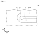
- FIG. FIG. 2 is a second plan view of printed wiring board 100.
- FIG. 3 is a cross-sectional view taken along line III-III in FIG.
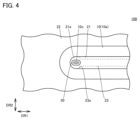
- FIG. 4 is a plan view of a printed wiring board 100 according to the first modification.
- FIG. 5 is an enlarged plan view of printed wiring board 100 according to the second modification.
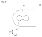
- FIG. 6 is an enlarged plan view of a printed wiring board 100 according to the third modification.
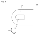
- FIG. 7 is an enlarged plan view of a printed wiring board 100 according to the fourth modification.
- FIG. 8 is an enlarged plan view of the printed wiring board 100 according to the fifth modification.
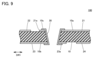
- FIG. 9 is a cross-sectional view of a printed wiring board 100 according to a sixth modification.
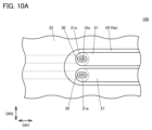
- FIG. 10A is a first plan view of a printed wiring board 100 according to the seventh modification.
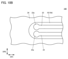
- FIG. 10B is a second plan view of printed wiring board 100 according to Modification 7.
- FIG. FIG. 11 is a manufacturing process diagram of the printed wiring board 100.
- FIG. 12 is a cross-sectional view illustrating the preparation step S1.
- FIG. 13 is a cross-sectional view illustrating the patterning step S2.
- FIG. 14 is a cross-sectional view illustrating the hole making step S3.
- FIG. 15 is a plan view of the printed wiring board 200.
- FIG. 16 is a cross-sectional view taken along line XVI-XVI in FIG.
- FIG. 17 shows the results of a simulation showing the relationship between the frequency of the signals flowing through the first signal pattern 21 and the second signal pattern 23 and the reflection characteristics at the connection portion between the first land 21a and the second land 23a.
- a conductor pattern (hereinafter referred to as a second conductor pattern) different from the first conductor pattern may be disposed on the second main surface.
- the second conductor pattern is aligned along a first direction in a plan view.
- the first conductor pattern and the second conductor pattern each have a first land and a second land at an end in the first direction.
- the first land and the second land overlap in a plan view.
- a through hole exposing the second land is formed in the dielectric substrate and the first land.
- the first land and the second land are electrically connected by a conductor layer formed by plating or the like on the inner wall surface of the through hole and on the second land exposed from the through hole.
- the through hole is formed in a circular shape in a plan view, and the opening area of the through hole becomes smaller as the first conductor pattern and the second conductor pattern are miniaturized, this may cause a failure in the connection between the first land and the second land by the conductor layer.
- the present disclosure has been made in consideration of the problems of the conventional technology as described above. More specifically, the present disclosure provides a printed wiring board that can suppress poor connections between lands of a signal pattern on one main surface of a board and lands of a signal pattern on the other main surface of the board.
- a printed wiring board includes a substrate, a first signal pattern, a second signal pattern, and a conductor layer.
- the substrate has a first main surface and a second main surface opposite the first main surface.
- the first signal pattern is disposed on the first main surface.
- the second signal pattern is disposed on the second main surface.
- the first signal pattern and the second signal pattern extend along a first direction in a planar view.
- the first signal pattern has a first land at an end in the first direction.
- the second signal pattern has a second land at an end in the first direction.
- the first land and the second land overlap in a planar view.
- a through hole exposing the second land is formed in the first land and the substrate.
- the first opening width which is the opening width of the through hole in the first direction, is larger than the second opening width of the through hole in a second direction perpendicular to the first direction.
- the conductor layer is disposed on an inner wall surface of the through hole and is electrically connected to the second land.
- the printed wiring board (1) above makes it possible to prevent poor connection between the first land and the second land.
- the value obtained by dividing the first opening width by the second opening width may be 3 or less. According to the printed wiring board of (2) above, it is possible to suppress poor connection between the first land and the second land while maintaining the reflection characteristics at the connection between the first land and the second portion.
- the through hole may have a tapered shape in which the opening area of the through hole decreases as it approaches the second land.
- a printed wiring board according to the embodiment is referred to as a printed wiring board 100.
- FIG. 1 is a first plan view of the printed wiring board 100.
- FIG. 2 is a second plan view of the printed wiring board 100.
- FIG. 2 shows a plan view of the printed wiring board 100 as viewed from the opposite side to that of FIG. 1.
- FIG. 3 is a cross-sectional view taken along line III-III in FIG. 2.
- the printed wiring board 100 has a substrate 10, a first signal pattern 21, a first ground pattern 22, a second signal pattern 23, a second ground pattern 24, and a conductor layer 30.
- a high-frequency signal is applied to the first signal pattern 21 and the second signal pattern 23 with reference to the first ground pattern 22 and the second ground pattern 24.
- the substrate 10 has a first main surface 10a and a second main surface 10b.
- the second main surface 10b is the opposite surface of the first main surface 10a.
- the first main surface 10a and the second main surface 10b are end surfaces in the thickness direction of the substrate 10.
- the substrate 10 is formed of an electrically insulating material.
- Specific examples of the constituent material of the substrate 10 include fluororesin, epoxy resin, polyimide, LCP (Liquid Crystal Polymer), etc.
- the constituent material of the substrate 10 may also be FRP (Fiber Reinforced Plastics) that includes any of fluororesin, epoxy resin, polyimide, etc., and glass cloth.
- FRP Fiber Reinforced Plastics
- the constituent material of the substrate 10 is not limited to this.
- a planar view is when the printed wiring board 100 is viewed along the normal direction of the first main surface 10a (second main surface 10b).
- One of the directions in the planar view is the first direction DR1
- the direction perpendicular to the first direction DR1 in the planar view is the second direction DR2.
- the thickness direction is the direction perpendicular to both the first direction DR1 and the second direction DR2.
- the first signal pattern 21 and the first ground pattern 22 are disposed on the first main surface 10a.
- the first signal pattern 21 extends along the first direction DR1 in a plan view.
- the first signal pattern 21 has a first land 21a at an end in the first direction DR1.
- the first ground pattern 22 surrounds the first signal pattern 21 in a plan view.
- the first ground pattern 22 is spaced apart from the first signal pattern 21.
- the second signal pattern 23 and the second ground pattern 24 are arranged on the second main surface 10b.
- the second signal pattern 23 extends along the first direction DR1 in a plan view.
- the second signal pattern 23 has a second land 23a at its end in the first direction DR1.
- the second ground pattern 24 surrounds the second signal pattern 23 in a plan view.
- the second ground pattern 24 is spaced apart from the second signal pattern 23.
- the first signal pattern 21, the first ground pattern 22, the second signal pattern 23, and the second ground pattern 24 are formed of a conductor such as a metal material.
- Specific examples of the constituent material of the first signal pattern 21, the first ground pattern 22, the second signal pattern 23, and the second ground pattern 24 include copper or a copper alloy.
- the constituent material of the first signal pattern 21, the first ground pattern 22, the second signal pattern 23, and the second ground pattern 24 is not limited to this.
- the first land 21a and the second land 23a are arranged so as to overlap in a plan view.
- a through hole 10c is formed in the first land 21a and the substrate 10.
- the through hole 10c penetrates the first land 21a in the thickness direction and also penetrates the substrate 10 in the thickness direction.
- the second land 23a is exposed from the lower end of the through hole 10c.
- the through hole 10c has a first opening width W1 and a second opening width W2.
- the first opening width W1 is the opening width of the through hole 10c in the first direction DR1.
- the second opening width W2 is the opening width of the through hole 10c in the second direction DR2.
- the first opening width W1 and the second opening width W2 are measured at the upper end of the through hole 10c.
- the first opening width W1 is larger than the second opening width W2.
- the longitudinal direction of the through hole 10c in a planar view is along the first direction DR1.
- the value obtained by dividing the first opening width W1 by the second opening width W2 may be, for example, 3 or less.
- the first opening width W1 may be 3 times or less the second opening width W2.
- the through hole 10c may be tapered in that the opening area becomes smaller as it approaches the second land 23a.
- the through hole 10c is, for example, elliptical in plan view.
- an ellipse is a shape formed by connecting two semicircular arcs with two straight lines.
- the conductor layer 30 is disposed on the inner wall surface of the through hole 10c and on the second land 23a exposed from the lower end of the through hole 10c.
- the conductor layer 30 may further be disposed on the first land 21a around the through hole 10c.
- the conductor layer 30 electrically connects the first land 21a and the second land 23a (the first signal pattern 21 and the second signal pattern 23).
- the conductor layer 30 is formed of a conductor such as a metal material.
- the conductor layer 30 is, for example, a plating layer (a layer formed by plating).
- Specific examples of materials constituting the conductor layer 30 include copper and copper alloys. However, the materials constituting the conductor layer 30 are not limited to these.
- a through hole other than through hole 10c is formed in first ground pattern 22 and substrate 10.
- the second ground pattern 24 is exposed from the lower end of this through hole.
- a conductor layer other than conductor layer 30 is formed on the inner wall surface of this through hole and on second ground pattern 24 exposed from the lower end of this through hole, so that first ground pattern 22 and second ground pattern 24 are electrically connected to each other.
- the first signal pattern 21 extends from one side (the right side in the figure) to the other side (the left side in the figure) in the first direction DR1, and the second signal pattern 23 also extends from one side to the other side in the first direction DR1. That is, in the example shown in Fig. 1 to Fig. 3, the first signal pattern 21 and the second signal pattern 23 are arranged so as not to overlap each other in a plan view, except for the first land 21a and the second land 23a.
- Fig. 4 is a plan view of the printed wiring board 100 according to the first modification. As shown in Fig. 4, the first signal pattern 21 and the second signal pattern 23 may extend along the first direction DR1 so as to overlap each other in a plan view.
- Fig. 5 is an enlarged plan view of the printed wiring board 100 according to the second modification. Note that the conductor layer 30 is omitted in Fig. 5.
- the through hole 10c may have an elliptical shape with the long axis direction along the first direction DR1 in a plan view.
- Fig. 6 is an enlarged plan view of the printed wiring board 100 according to the third modification. The conductor layer 30 is omitted in Fig. 6.
- the through hole 10c may have a dumbbell shape with the longitudinal direction along the first direction DR1 in a plan view.
- FIG. 7 is an enlarged plan view of the printed wiring board 100 according to the fourth modification. Note that the conductor layer 30 is omitted from FIG. 7. As shown in FIG. 7, the through hole 10c may have a shape that combines a rectangular shape whose longitudinal direction is along the first direction DR1 and a semicircle in a plan view. FIG. 8 is an enlarged plan view of the printed wiring board 100 according to the fifth modification. The conductor layer 30 is omitted from FIG. 8. As shown in FIG. 8, the through hole 10c may have a rectangular shape whose longitudinal direction is along the first direction DR1 in a plan view. In short, the planar shape of the through hole 10c is not particularly limited as long as the first opening width W1 is larger than the second opening width W2.
- (Variation 6) 9 is a cross-sectional view of the printed wiring board 100 according to the sixth modification.
- the through hole 10c may further penetrate the second land 23a.
- the conductor layer 30 is also disposed on the second land 23a around the through hole 10c. The conductor layer 30 may be electrically connected to the second land 23a in this manner.
- the through hole for connecting the first ground pattern 22 and the second ground pattern 24 penetrates the substrate 10, the first ground pattern 22, and the second ground pattern 24, and the first ground pattern 22 and the second ground pattern 24 are electrically connected by disposing the conductor layer on the inner wall surface of the through hole, on the first ground pattern 22 around the through hole, and on the second ground pattern 24 around the through hole.
- Fig. 10A is a first plan view of the printed wiring board 100 according to the seventh modification.
- Fig. 10B is a second plan view of the printed wiring board 100 according to the seventh modification.
- the printed wiring board 100 may have a pair of first signal patterns 21 and a pair of second signal patterns 23, and these signal patterns may form a differential signal line.
- the printed wiring board 100 is a single-layer board has been described, but the printed wiring board 100 may be a multi-layer board.
- FIG. 11 is a manufacturing process diagram of the printed wiring board 100.
- the manufacturing method of the printed wiring board 100 includes a preparation process S1, a patterning process S2, a hole drilling process S3, and a conductor layer forming process S4.
- the patterning process S2 is performed after the preparation process S1.
- the hole drilling process S3 is performed after the patterning process S2.
- the conductor layer forming process S4 is performed after the hole drilling process S3.
- FIG. 12 is a cross-sectional view illustrating the preparation step S1. As shown in FIG. 12, in the preparation step S1, the substrate 10 is prepared. At this point, copper foil 25 and copper foil 26 are disposed on the first main surface 10a and the second main surface 10b, respectively.
- FIG. 13 is a cross-sectional view explaining the patterning step S2.
- the copper foil 25 and the copper foil 26 are patterned to form the first signal pattern 21, the first ground pattern 22, the second signal pattern 23, and the second ground pattern 24.
- the copper foil 25 and the copper foil 26 are patterned by etching using the resist patterns formed on the copper foil 25 and the copper foil 26 as a mask.
- the resist pattern is formed by applying a dry film resist to the copper foil 25 and the copper foil 26, and exposing and developing the applied dry film resist.
- FIG. 14 is a cross-sectional view illustrating the hole-making process S3.
- a through hole 10c is formed at a position where the first land 21a and the second land 23a overlap in a plan view.
- the through hole 10c is formed, for example, by irradiating a laser.
- the through hole 10c may also be formed, for example, by performing a drilling process.
- a conductor layer 30 is formed on the inner wall surface of the through hole 10c, on the second land 23a exposed from the lower end of the through hole 10c, and on the first land 21a around the through hole 10c.
- the conductor layer 30 is formed, for example, by electrolytic plating or electroless plating. In this manner, the structure of the printed wiring board 100 shown in Figures 1 to 3 is formed.
- the conductor layer 30 may be formed over the entire surfaces of the first signal pattern 21 and the first ground pattern 22, in addition to the inner wall surface of the through hole 10c and the second land 23a exposed from the lower end of the through hole 10c.
- panel plating may be performed in the conductor layer formation process S4.
- FIG. 15 is a plan view of printed wiring board 200.
- FIG. 16 is a cross-sectional view taken along line XVI-XVI of FIG. 15. As shown in FIGS. 15 and 16, in printed wiring board 200, first opening width W1 is equal to second opening width W2. In other words, in printed wiring board 200, through hole 10c is circular in plan view. Except for this, the configuration of printed wiring board 200 is the same as the configuration of printed wiring board 100.
- the second opening width W2 also becomes smaller accordingly.
- the first opening width W1 is equal to the second opening width W2 as in the printed wiring board 200
- the first opening width W1 also becomes smaller as the second opening width W2 becomes smaller.
- the opening area at the bottom end of the through hole 10c becomes too small, making it difficult for the conductor layer 30 to be formed on the second land 23a exposed from the bottom end of the through hole 10c, which may cause a connection failure between the first land 21a and the second land 23a. This becomes more noticeable when the through hole 10c is tapered so that the opening area becomes smaller as it approaches the bottom end.
- the first opening width W1 is larger than the second opening width W2.
- the first opening width W1 can be maintained, so that the opening area at the lower end of the through hole 10c can be secured. In this way, the printed wiring board 100 can suppress poor connections between the first land 21a and the second land 23a.
- FIG. 17 shows the results of a simulation showing the relationship between the frequency of the signal flowing through the first signal pattern 21 and the second signal pattern 23 and the reflection characteristics at the connection between the first land 21a and the second land 23a.
- Samples 1 and 2 were used for the simulation shown in FIG. 17.
- Samples 1 and 2 correspond to the printed wiring board 100 and the printed wiring board 200, respectively.
- the through hole 10c was an ellipse with a first opening width W1 of 0.2 mm and a second opening width W2 of 0.1 mm.
- the through hole 10c was a circle with a first opening width W1 and a second opening width W2 of 0.1 mm.
- the horizontal axis in FIG. 17 shows the frequency (in GHz) of the high-frequency signal flowing through the first signal pattern 21 and the second signal pattern 23, and the vertical axis in FIG. 17 shows the voltage standing wave ratio (VSWR), which is an index of the reflection characteristics.
- VSWR voltage standing wave ratio
- the reflection characteristics at the connection between the first land 21a and the second land 23a deteriorate.
- the reflection characteristics at the connection between the first land 21a and the second land 23a are maintained even if the first opening width W1 is increased.
- the value obtained by dividing the first opening width W1 by the second opening width W2 is 3 or less, the reflection characteristics at the connection between the first land 21a and the second land 23a are maintained.
Landscapes
- Engineering & Computer Science (AREA)
- Microelectronics & Electronic Packaging (AREA)
- Structure Of Printed Boards (AREA)
Abstract
プリント配線板は、基板と、第1信号パターンと、第2信号パターンと、導体層とを備えている。基板は、第1主面と第1主面の反対面である第2主面とを有する。第1信号パターンは、第1主面上に配置されている。第2信号パターンは、第2主面上に配置されている。第1信号パターン及び第2信号パターンは、平面視において、第1方向に沿って延在している。第1信号パターンは、第1方向における端に第1ランドを有する。第2信号パターンは、第1方向における端に第2ランドを有する。第1ランド及び第2ランドは、平面視において重なっている。第1ランド及び基板には、第2ランドを露出させる貫通穴が形成されている。
Description
本開示は、プリント配線板に関する。本出願は、2023年11月7日に出願した日本特許出願である特願2023-190111号に基づく優先権を主張する。当該日本特許出願に記載された全ての記載内容は、参照によって本明細書に援用される。
例えば特開2000-216603号公報(特許文献1)には、プリント配線板が記載されている。特許文献1に記載のプリント配線板は、誘電体基板と、第1導体パターンとを有している。誘電体基板は、第1主面と第1主面の反対面である第2主面とを有している。第1導体パターンは、第1主面上に配置されている。第1導体パターンは、平面視において第1方向に延在している。
本開示のプリント配線板は、基板と、第1信号パターンと、第2信号パターンと、導体層とを備えている。基板は、第1主面と第1主面の反対面である第2主面とを有する。第1信号パターンは、第1主面上に配置されている。第2信号パターンは、第2主面上に配置されている。第1信号パターン及び第2信号パターンは、平面視において、第1方向に沿って延在している。第1信号パターンは、第1方向における端に第1ランドを有する。第2信号パターンは、第1方向における端に第2ランドを有する。第1ランド及び第2ランドは、平面視において重なっている。第1ランド及び基板には、第2ランドを露出させる貫通穴が形成されている。貫通穴の第1方向における開口幅である第1開口幅は、貫通穴の第1方向に垂直な第2方向における第2開口幅よりも大きい。導体層は、貫通穴の内壁面上に配置されており、第2ランドに電気的に接続されている。
[本開示が解決しようとする課題]
第1導体パターンとは別の導体パターン(第2導体パターンとする)が、第2主面上に配置されていることがある。第2導体パターンは、平面視において、第1方向に沿っている。この場合、第1導体パターン及び第2導体パターンは、それぞれ、第1方向における端に第1ランド及び第2ランドを有する。第1ランド及び第2ランドは、平面視において重なる。誘電体基板及び第1ランドには、第2ランドを露出させる貫通穴が形成される。第1ランド及び第2ランドは、貫通穴の内壁面上及び貫通穴から露出している第2ランド上にめっき等で形成された導体層により電気的に接続される。
第1導体パターンとは別の導体パターン(第2導体パターンとする)が、第2主面上に配置されていることがある。第2導体パターンは、平面視において、第1方向に沿っている。この場合、第1導体パターン及び第2導体パターンは、それぞれ、第1方向における端に第1ランド及び第2ランドを有する。第1ランド及び第2ランドは、平面視において重なる。誘電体基板及び第1ランドには、第2ランドを露出させる貫通穴が形成される。第1ランド及び第2ランドは、貫通穴の内壁面上及び貫通穴から露出している第2ランド上にめっき等で形成された導体層により電気的に接続される。
貫通穴が平面視において円形に形成されると、第1導体パターン及び第2導体パターンが微細化されるに伴って貫通穴の開口面積が小さくなる場合、導体層による第1ランドと第2ランドとの接続に不良が生じることがある。
本開示は、上記のような従来技術の問題点に鑑みてなされたものである。より具体的には、本開示は、基板の一方の主面上にある信号パターンのランドと基板の他方の主面上にある信号パターンのランドとの間の接続不良を抑制可能なプリント配線板を提供するものである。
[本開示の効果]
本開示のプリント配線板によると、基板の一方の主面上にある信号パターンのランドと基板の他方の主面上にある信号パターンのランドとの間の接続不良を抑制可能である。
本開示のプリント配線板によると、基板の一方の主面上にある信号パターンのランドと基板の他方の主面上にある信号パターンのランドとの間の接続不良を抑制可能である。
[本開示の実施形態の説明]
まず、本開示の実施形態を列記して説明する。
まず、本開示の実施形態を列記して説明する。
(1)一実施形態に係るプリント配線板は、基板と、第1信号パターンと、第2信号パターンと、導体層とを備える。基板は、第1主面と第1主面の反対面である第2主面とを有する。第1信号パターンは、第1主面上に配置されている。第2信号パターンは、第2主面上に配置されている。第1信号パターン及び第2信号パターンは、平面視において第1方向に沿って延在している。第1信号パターンは、第1方向における端に第1ランドを有する。第2信号パターンは、第1方向における端に第2ランドを有する。第1ランド及び第2ランドは、平面視において重なっている。第1ランド及び基板には、第2ランドを露出させる貫通穴が形成されている。貫通穴の第1方向における開口幅である第1開口幅は、貫通穴の第1方向に垂直な第2方向における第2開口幅よりも大きい。導体層は、貫通穴の内壁面上に配置されており、第2ランドに電気的に接続されている。上記(1)のプリント配線板によると、第1ランドと第2ランドとの間の接続不良を抑制可能である。
(2)上記(1)のプリント配線板では、第1開口幅を第2開口幅で除した値が3以下であってもよい。上記(2)のプリント配線板によると、第1ランドと第2部分との間の接続部における反射特性を維持しつつ、第1ランドと第2ランドとの間の接続不良を抑制可能である。
(3)上記(1)又は(2)のプリント配線板では、貫通穴が、第2ランドに近づくにつれて貫通穴の開口面積が小さくなるテーパ形状であってもよい。
[本開示の実施形態の詳細]
次に、本開示の実施形態の詳細を、図面を参照しながら説明する。以下の図面では、同一又は相当する部分に同一の参照符号を付し、重複する説明は繰り返さない。実施形態に係るプリント配線板を、プリント配線板100とする。
次に、本開示の実施形態の詳細を、図面を参照しながら説明する。以下の図面では、同一又は相当する部分に同一の参照符号を付し、重複する説明は繰り返さない。実施形態に係るプリント配線板を、プリント配線板100とする。
(プリント配線板100の構成)
以下に、プリント配線板100の構成を説明する。
以下に、プリント配線板100の構成を説明する。
図1は、プリント配線板100の第1の平面図である。図2は、プリント配線板100の第2の平面図である。図2には、図1とは反対側から見たプリント配線板100の平面図が示されている。図3は、図2のIII-IIIにおける断面図である。図1から図3に示されるように、プリント配線板100は、基板10と、第1信号パターン21と、第1グランドパターン22と、第2信号パターン23と、第2グランドパターン24と、導体層30とを有している。第1信号パターン21及び第2信号パターン23には、第1グランドパターン22及び第2グランドパターン24を基準として、高周波信号が印加される。
基板10は、第1主面10aと第2主面10bとを有している。第2主面10bは、第1主面10aの反対面である。第1主面10a及び第2主面10bは、基板10の厚さ方向における端面である。基板10は、電気絶縁性の材料で形成されている。基板10の構成材料の具体例としては、例えばフッ素樹脂、エポキシ樹脂、ポリイミド、LCP(Liquid Crystal Polymer)等が挙げられる。また、基板10の構成材料は、フッ素樹脂、エポキシ樹脂及びポリイミド等のうちのいずれかとガラスクロスとを含むFRP(Fiber Reinforced Plastics)であってもよい。但し、基板10の構成材料はこれに限られない。
平面視とは、第1主面10a(第2主面10b)の法線方向に沿ってプリント配線板100を見る場合である。平面視における方向の1つを第1方向DR1とし、平面視において第1方向DR1に垂直な方向を第2方向DR2とする。厚さ方向とは、第1方向DR1及び第2方向DR2の双方に垂直な方向である。
第1信号パターン21及び第1グランドパターン22は、第1主面10a上に配置されている。第1信号パターン21は、平面視において、第1方向DR1に沿って延在している。第1信号パターン21は、第1方向DR1における端に第1ランド21aを有している。第1グランドパターン22は、平面視において、第1信号パターン21を取り囲んでいる。第1グランドパターン22は、第1信号パターン21から離間している。
第2信号パターン23及び第2グランドパターン24は、第2主面10b上に配置されている。第2信号パターン23は、平面視において、第1方向DR1に沿って延在している。第2信号パターン23は、第1方向DR1における端に第2ランド23aを有している。第2グランドパターン24は、平面視において、第2信号パターン23を取り囲んでいる。第2グランドパターン24は、第2信号パターン23から離間している。
第1信号パターン21、第1グランドパターン22、第2信号パターン23及び第2グランドパターン24は、金属材料等の導体で形成されている。第1信号パターン21、第1グランドパターン22、第2信号パターン23及び第2グランドパターン24の構成材料の具体例としては、銅又は銅合金が挙げられる。但し、第1信号パターン21、第1グランドパターン22、第2信号パターン23及び第2グランドパターン24の構成材料はこれに限られない。
第1ランド21a及び第2ランド23aは、平面視において重なるように配置されている。第1ランド21a及び基板10には、貫通穴10cが形成されている。貫通穴10cは、第1ランド21aを厚さ方向に貫通しているとともに、基板10を厚さ方向に貫通している。貫通穴10cの下端からは、第2ランド23aが露出している。
貫通穴10cは、第1開口幅W1と、第2開口幅W2とを有している。第1開口幅W1は、貫通穴10cの第1方向DR1における開口幅である。第2開口幅W2は、貫通穴10cの第2方向DR2における開口幅である。第1開口幅W1及び第2開口幅W2は、貫通穴10cの上端において測定される。第1開口幅W1は第2開口幅W2よりも大きい。このことを別の観点から言えば、平面視における貫通穴10cの長手方向は、第1方向DR1に沿っている。
第1開口幅W1を第2開口幅W2で除した値は、例えば3以下であってもよい。すなわち、第1開口幅W1は、第2開口幅W2の3倍以下であってもよい。貫通穴10cは、開口面積が第2ランド23aに近づくにつれて小さくなっているテーパ状であってもよい。貫通穴10cは、平面視において、例えば長円形状である。ここで、長円とは、2つの半円弧を2つの直線で接続した形状である。
導体層30は、貫通穴10cの内壁面上及び貫通穴10cの下端から露出している第2ランド23a上に配置されている。導体層30は、貫通穴10cの周囲にある第1ランド21a上にさらに配置されていてもよい。導体層30により、第1ランド21aと第2ランド23aとが(第1信号パターン21と第2信号パターン23とが)電気的に接続されている。
導体層30は、金属材料等の導体で形成されている。導体層30は、例えば、めっき層(めっきにより形成される層)である。導体層30の構成材料の具体例としては、銅又は銅合金が挙げられる。但し、導体層30の構成材料は、これに限られるものではない。
図示されていないが、第1グランドパターン22及び基板10には、貫通穴10cとは別の貫通穴が形成されている。この貫通穴の下端からは、第2グランドパターン24が露出している。この貫通穴の内壁面上及びこの貫通穴の下端から露出している第2グランドパターン24上に導体層30とは別の導体層が形成されることにより、第1グランドパターン22と第2グランドパターン24とが互いに電気的に接続されている。
(変形例1)
図1から図3に示されている例では、第1信号パターン21が第1方向DR1において一方側(図中で右側)から他方側(図中で左側)に延在し、第2信号パターン23も第1方向DR1において一方側から他方側に延在している。すなわち、図1から図3に示されている例では、第1信号パターン21及び第2信号パターン23が、平面視において、第1ランド21a及び第2ランド23aを除いて互いに重ならないように配置されている。図4は、変形例1に係るプリント配線板100の平面図である。図4に示されているように、第1信号パターン21及び第2信号パターン23は、平面視において互いに重なるように第1方向DR1に沿って延在していてもよい。
図1から図3に示されている例では、第1信号パターン21が第1方向DR1において一方側(図中で右側)から他方側(図中で左側)に延在し、第2信号パターン23も第1方向DR1において一方側から他方側に延在している。すなわち、図1から図3に示されている例では、第1信号パターン21及び第2信号パターン23が、平面視において、第1ランド21a及び第2ランド23aを除いて互いに重ならないように配置されている。図4は、変形例1に係るプリント配線板100の平面図である。図4に示されているように、第1信号パターン21及び第2信号パターン23は、平面視において互いに重なるように第1方向DR1に沿って延在していてもよい。
(変形例2から変形例5)
図5は、変形例2に係るプリント配線板100の拡大された平面図である。なお、図5中では、導体層30の図示が省略されている。図5に示されているように、貫通穴10cは、平面視において長軸方向が第1方向DR1に沿う楕円形状であってもよい。図6は、変形例3に係るプリント配線板100の拡大された平面図である。図6中では、導体層30の図示が省略されている。図6に示されているように、貫通穴10cは、平面視において、長手方向が第1方向DR1に沿う亜鈴形状であってもよい。
図5は、変形例2に係るプリント配線板100の拡大された平面図である。なお、図5中では、導体層30の図示が省略されている。図5に示されているように、貫通穴10cは、平面視において長軸方向が第1方向DR1に沿う楕円形状であってもよい。図6は、変形例3に係るプリント配線板100の拡大された平面図である。図6中では、導体層30の図示が省略されている。図6に示されているように、貫通穴10cは、平面視において、長手方向が第1方向DR1に沿う亜鈴形状であってもよい。
図7は、変形例4に係るプリント配線板100の拡大された平面図である。なお、図7中では、導体層30の図示が省略されている。図7に示されているように、貫通穴10cは、平面視において、長手方向が第1方向DR1に沿う矩形形状と半円とを組み合わせた形状であってもよい。図8は、変形例5に係るプリント配線板100の拡大された平面図である。図8中では、導体層30の図示が省略されている。図8に示されているように、貫通穴10cは、平面視において、長手方向が第1方向DR1に沿う矩形形状であってもよい。要するに、貫通穴10cの平面形状は、第1開口幅W1が第2開口幅W2よりも大きければ特に限定されない。
(変形例6)
図9は、変形例6に係るプリント配線板100の断面図である。上記においては貫通穴10cが基板10と第1ランド21aを貫通する例を示したが、図9に示されているように、貫通穴10cは、第2ランド23aをさらに貫通していてもよい。この場合、導体層30は、貫通穴10cの周囲にある第2ランド23a上にも配置されている。導体層30は、このようにして第2ランド23aに電気的に接続されていてもよい。図示されていないが、この場合、第1グランドパターン22と第2グランドパターン24とを接続するための貫通穴は基板10、第1グランドパターン22及び第2グランドパターン24を貫通しており、当該貫通穴の内壁面上、当該貫通穴の周囲にある第1グランドパターン22上及び当該貫通穴の周囲にある第2グランドパターン24上に導体層が配置されることにより第1グランドパターン22と第2グランドパターン24とが電気的に接続されている。
図9は、変形例6に係るプリント配線板100の断面図である。上記においては貫通穴10cが基板10と第1ランド21aを貫通する例を示したが、図9に示されているように、貫通穴10cは、第2ランド23aをさらに貫通していてもよい。この場合、導体層30は、貫通穴10cの周囲にある第2ランド23a上にも配置されている。導体層30は、このようにして第2ランド23aに電気的に接続されていてもよい。図示されていないが、この場合、第1グランドパターン22と第2グランドパターン24とを接続するための貫通穴は基板10、第1グランドパターン22及び第2グランドパターン24を貫通しており、当該貫通穴の内壁面上、当該貫通穴の周囲にある第1グランドパターン22上及び当該貫通穴の周囲にある第2グランドパターン24上に導体層が配置されることにより第1グランドパターン22と第2グランドパターン24とが電気的に接続されている。
(変形例7及び変形例8)
図10Aは、変形例7に係るプリント配線板100の第1の平面図である。また、図10Bは、変形例7に係るプリント配線板100の第2の平面図である。上記においては第1信号パターン21及び第2信号パターン23が1つの場合、すなわちシングルエンドの信号線路の場合の例を説明したが、図10A及び図10Bに示されているようにプリント配線板100は1対の第1信号パターン21及び1対の第2信号パターン23を有していてもよく、これらの信号パターンにより差動信号線路が構成されていてもよい。上記においては、プリント配線板100が単層基板である場合の例を説明したが、プリント配線板100は多層基板であってもよい。
図10Aは、変形例7に係るプリント配線板100の第1の平面図である。また、図10Bは、変形例7に係るプリント配線板100の第2の平面図である。上記においては第1信号パターン21及び第2信号パターン23が1つの場合、すなわちシングルエンドの信号線路の場合の例を説明したが、図10A及び図10Bに示されているようにプリント配線板100は1対の第1信号パターン21及び1対の第2信号パターン23を有していてもよく、これらの信号パターンにより差動信号線路が構成されていてもよい。上記においては、プリント配線板100が単層基板である場合の例を説明したが、プリント配線板100は多層基板であってもよい。
(プリント配線板100の製造方法)
以下に、プリント配線板100の製造方法を説明する。
以下に、プリント配線板100の製造方法を説明する。
図11は、プリント配線板100の製造工程図である。図11に示されるように、プリント配線板100の製造方法は、準備工程S1と、パターンニング工程S2と、穴開け工程S3と、導体層形成工程S4とを有している。パターンニング工程S2は、準備工程S1の後に行われる。穴開け工程S3は、パターンニング工程S2の後に行われる。導体層形成工程S4は、穴開け工程S3の後に行われる。
図12は、準備工程S1を説明する断面図である。図12に示されているように、準備工程S1では、基板10が準備される。この時点で、第1主面10a上及び第2主面10b上には、それぞれ銅箔25及び銅箔26が配置されている。
図13は、パターンニング工程S2を説明する断面図である。図13に示されているように、パターンニング工程S2では、銅箔25及び銅箔26がパターンニングされることにより、第1信号パターン21、第1グランドパターン22、第2信号パターン23及び第2グランドパターン24が形成される。銅箔25及び銅箔26のパターンニングは、銅箔25上及び銅箔26上に形成されたレジストパターンをマスクとするエッチングにより行われる。レジストパターンは、銅箔25上及び銅箔26上にドライフィルムレジストを貼付するとともに、貼付されたドライフィルムレジストを露光・現像することにより形成される。
図14は、穴開け工程S3を説明する断面図である。図14に示されているように、穴開け工程S3では、平面視において第1ランド21a及び第2ランド23aが重なる位置に、貫通穴10cが形成される。貫通穴10cは、例えば、レーザを照射することにより形成される。貫通穴10cは、例えばドリル加工を行うことにより形成されてもよい。
導体層形成工程S4では、貫通穴10cの内壁面上及び貫通穴10cの下端から露出している第2ランド23a上並びに貫通穴10cの周囲にある第1ランド21a上に、導体層30が形成される。導体層30は、例えば、電解めっき法又は無電解めっき法により形成される。以上のようにして、図1から図3に示されているプリント配線板100の構造が形成される。
なお、導体層30は、貫通穴10cの内壁面上及び貫通穴10cの下端から露出している第2ランド23a上に加えて、第1信号パターン21や第1グランドパターン22上の全面にわたって形成されてもよい。つまり、導体層形成工程S4では、パネルめっきが行われてもよい。
(プリント配線板100の効果)
以下に、プリント配線板100の効果を、比較例に係るプリント配線板と対比しながら説明する。なお、比較例に係るプリント配線板を、プリント配線板200とする。
以下に、プリント配線板100の効果を、比較例に係るプリント配線板と対比しながら説明する。なお、比較例に係るプリント配線板を、プリント配線板200とする。
図15は、プリント配線板200の平面図である。図16は、図15のXVI-XVIにおける断面図である。図15及び図16に示されているように、プリント配線板200では、第1開口幅W1が第2開口幅W2に等しい。つまり、プリント配線板200では、貫通穴10cが、平面視において円形である。この点を除いて、プリント配線板200の構成は、プリント配線板100の構成と共通している。
第1信号パターン21及び第2信号パターン23の幅が狭くなると、それに応じて第2開口幅W2も小さくなる。プリント配線板200のように第1開口幅W1が第2開口幅W2に等しいと、第2開口幅W2が小さくなるに伴って第1開口幅W1も小さくなる。そうすると、貫通穴10cの下端における開口面積が小さくなり過ぎ、導体層30が貫通穴10cの下端から露出している第2ランド23a上に形成されがたくなり、第1ランド21aと第2ランド23aとの間で接続不良が発生するおそれがある。このことは、貫通穴10cが下端に近づくにつれて開口面積が小さくなるテーパ状である場合に、より顕著になる。
他方で、プリント配線板100では、第1開口幅W1が第2開口幅W2よりも大きくなっている。その結果、プリント配線板100では、第1信号パターン21や第2信号パターン23の幅が狭くなって第2開口幅W2が小さくなっても第1開口幅W1を維持できるため、貫通穴10cの下端における開口面積を確保することができる。このように、プリント配線板100によると、第1ランド21aと第2ランド23aとの間の接続不良を抑制可能である。
図17は、第1信号パターン21及び第2信号パターン23を流れる信号の周波数と第1ランド21a及び第2ランド23aの接続部における反射特性のとの関係を示すシミュレーション結果である。図17に示されているシミュレーションには、サンプル1及びサンプル2が供された。サンプル1及びサンプル2は、それぞれ、プリント配線板100及びプリント配線板200に対応している。サンプル1では、貫通穴10cが、第1開口幅W1が0.2mm、第2開口幅W2が0.1mmの長円形とされた。サンプル2では、貫通穴10cが、第1開口幅W1及び第2開口幅W2が0.1mmの円形とされた。図17中の横軸は第1信号パターン21及び第2信号パターン23を流れる高周波信号の周波数(単位はGHz)であり、図17中の縦軸は反射特性の指標となる電圧定在波比(VSWR)である。
第1開口幅W1を第2開口幅W2で除した値が大きくなるにつれて、第1ランド21aと第2ランド23aとの接続部における反射特性が劣化する。しかしながら、図14に示されているように、第1開口幅W1を第2開口幅W2で除した値が2である場合には、第1開口幅W1を大きくしても、第1ランド21aと第2ランド23aとの接続部における反射特性が維持されている。図示されていないが、同様のシミュレーションでは、第1開口幅W1を第2開口幅W2で除した値が3以下であれば、第1ランド21aと第2ランド23aとの接続部における反射特性が維持される。
今回開示された実施形態は全ての点で例示であって、制限的なものではないと考えられるべきである。本発明の範囲は上記の実施形態ではなく請求の範囲によって示され、請求の範囲と均等の意味及び範囲内での全ての変更が含まれることが意図される。
100 プリント配線板、200 プリント配線板、10 基板、10a 第1主面、10b 第2主面、10c 貫通穴、21 第1信号パターン、21a 第1ランド、22 第1グランドパターン、23 第2信号パターン、23a 第2ランド、24 第2グランドパターン、25,26 銅箔、30 導体層、DR1 第1方向、DR2 第2方向、S1 準備工程、S2 パターンニング工程、S3 穴開け工程、S4 導体層形成工程、W1 第1開口幅、W2 第2開口幅。
Claims (3)
- 基板と、
第1信号パターンと、
第2信号パターンと、
導体層とを備え、
前記基板は、第1主面と前記第1主面の反対面である第2主面とを有し、
前記第1信号パターンは、前記第1主面上に配置されており、
前記第2信号パターンは、前記第2主面上に配置されており、
前記第1信号パターン及び前記第2信号パターンは、平面視において、第1方向に沿って延在しており、
前記第1信号パターンは、前記第1方向における端に第1ランドを有し、
前記第2信号パターンは、前記第1方向における端に第2ランドを有し、
前記第1ランド及び前記第2ランドは、平面視において重なっており、
前記第1ランド及び前記基板には、貫通穴が形成されており、
前記貫通穴の前記第1方向における開口幅である第1開口幅は、前記貫通穴の前記第1方向に垂直な第2方向における第2開口幅よりも大きく、
前記導体層は、前記貫通穴の内壁面上に配置されており、前記第2ランドに電気的に接続されている、プリント配線板。 - 前記第1開口幅を前記第2開口幅で除した値は、3以下である、請求項1に記載のプリント配線板。
- 前記貫通穴は、前記第2ランドに近づくにつれて前記貫通穴の開口面積が小さくなるテーパ形状である、請求項1又は請求項2に記載のプリント配線板。
Applications Claiming Priority (2)
| Application Number | Priority Date | Filing Date | Title |
|---|---|---|---|
| JP2023-190111 | 2023-11-07 | ||
| JP2023190111 | 2023-11-07 |
Publications (1)
| Publication Number | Publication Date |
|---|---|
| WO2025100113A1 true WO2025100113A1 (ja) | 2025-05-15 |
Family
ID=95695102
Family Applications (1)
| Application Number | Title | Priority Date | Filing Date |
|---|---|---|---|
| PCT/JP2024/033628 Pending WO2025100113A1 (ja) | 2023-11-07 | 2024-09-20 | プリント配線板 |
Country Status (1)
| Country | Link |
|---|---|
| WO (1) | WO2025100113A1 (ja) |
Citations (3)
| Publication number | Priority date | Publication date | Assignee | Title |
|---|---|---|---|---|
| JPH06216488A (ja) * | 1993-01-19 | 1994-08-05 | Canon Inc | プリント配線板及びその加工方法 |
| JP2002064274A (ja) * | 2000-08-21 | 2002-02-28 | Toppan Printing Co Ltd | ビアホール構造とその形成方法およびこれを用いた多層配線基板 |
| WO2022176853A1 (ja) * | 2021-02-22 | 2022-08-25 | 京セラ株式会社 | 印刷配線板 |
-
2024
- 2024-09-20 WO PCT/JP2024/033628 patent/WO2025100113A1/ja active Pending
Patent Citations (3)
| Publication number | Priority date | Publication date | Assignee | Title |
|---|---|---|---|---|
| JPH06216488A (ja) * | 1993-01-19 | 1994-08-05 | Canon Inc | プリント配線板及びその加工方法 |
| JP2002064274A (ja) * | 2000-08-21 | 2002-02-28 | Toppan Printing Co Ltd | ビアホール構造とその形成方法およびこれを用いた多層配線基板 |
| WO2022176853A1 (ja) * | 2021-02-22 | 2022-08-25 | 京セラ株式会社 | 印刷配線板 |
Similar Documents
| Publication | Publication Date | Title |
|---|---|---|
| US7569773B2 (en) | Wired circuit board | |
| US6072375A (en) | Waveguide with edge grounding | |
| US6039889A (en) | Process flows for formation of fine structure layer pairs on flexible films | |
| KR20020022126A (ko) | 플렉시블 배선판 및 플렉시블 배선판의 제조방법 | |
| US8040198B2 (en) | Printed wiring board having wire grounding conductors with distances that are 1/n the width of the signal lines | |
| WO2025100113A1 (ja) | プリント配線板 | |
| CN115190707A (zh) | 一种电路板的制造方法 | |
| JP2008235697A (ja) | 配線回路基板およびその製造方法 | |
| WO2024166888A1 (ja) | プリント配線板 | |
| KR20050046565A (ko) | 양면 배선 회로 기판 | |
| JP2016127248A (ja) | 多層配線基板 | |
| WO2024057586A1 (ja) | プリント配線板の製造方法 | |
| CN115348741A (zh) | 减成法细线路电路板制造方法 | |
| JP2023003107A (ja) | 配線板 | |
| US7334325B2 (en) | Apparatus and method for improving coupling across plane discontinuities on circuit boards | |
| JP2014022625A (ja) | プリント配線基板及びその製造方法 | |
| WO2026018492A1 (ja) | プリント配線板 | |
| TWI822197B (zh) | 電路板結構及其製作方法 | |
| US20260059649A1 (en) | Signaling Trace with Width-Modulated Discontinuity Mitigation | |
| TWI737425B (zh) | 內埋式線路板及其製作方法 | |
| US12403673B2 (en) | Resin multilayer substrate and method for manufacturing resin multilayer substrate | |
| CN111954366B (zh) | 电路板结构及其制造方法 | |
| TW202042606A (zh) | 電路板結構及其製造方法 | |
| JP2005322946A (ja) | プリント配線板の製造方法及びプリント配線板 | |
| WO2025009357A1 (ja) | フレキシブルプリント配線板の製造方法及びフレキシブルプリント配線板 |
Legal Events
| Date | Code | Title | Description |
|---|---|---|---|
| 121 | Ep: the epo has been informed by wipo that ep was designated in this application |
Ref document number: 24888413 Country of ref document: EP Kind code of ref document: A1 |