WO2025094313A1 - 電力変換装置及び電力変換装置のインダクタ電流制御方法 - Google Patents
電力変換装置及び電力変換装置のインダクタ電流制御方法 Download PDFInfo
- Publication number
- WO2025094313A1 WO2025094313A1 PCT/JP2023/039448 JP2023039448W WO2025094313A1 WO 2025094313 A1 WO2025094313 A1 WO 2025094313A1 JP 2023039448 W JP2023039448 W JP 2023039448W WO 2025094313 A1 WO2025094313 A1 WO 2025094313A1
- Authority
- WO
- WIPO (PCT)
- Prior art keywords
- current
- power conversion
- duty ratio
- inductor
- output
- Prior art date
- Legal status (The legal status is an assumption and is not a legal conclusion. Google has not performed a legal analysis and makes no representation as to the accuracy of the status listed.)
- Pending
Links
Images















Classifications
-
- H—ELECTRICITY
- H02—GENERATION; CONVERSION OR DISTRIBUTION OF ELECTRIC POWER
- H02M—APPARATUS FOR CONVERSION BETWEEN AC AND AC, BETWEEN AC AND DC, OR BETWEEN DC AND DC, AND FOR USE WITH MAINS OR SIMILAR POWER SUPPLY SYSTEMS; CONVERSION OF DC OR AC INPUT POWER INTO SURGE OUTPUT POWER; CONTROL OR REGULATION THEREOF
- H02M3/00—Conversion of DC power input into DC power output
- H02M3/22—Conversion of DC power input into DC power output with intermediate conversion into AC
- H02M3/24—Conversion of DC power input into DC power output with intermediate conversion into AC by static converters
- H02M3/28—Conversion of DC power input into DC power output with intermediate conversion into AC by static converters using discharge tubes with control electrode or semiconductor devices with control electrode to produce the intermediate AC
Definitions
- This disclosure relates to a power conversion device and a method for controlling the inductor current of the power conversion device.
- Power conversion devices such as DC-DC converters that convert input voltages into a target output voltage need to output an output voltage without distortion.
- a multi-phase configuration in which multiple DC-DC converters are connected in parallel is used.
- the power conversion device disclosed in Patent Document 1 is not a multi-phase configuration, but is equivalent to a DC-DC converter with one phase.
- the power conversion device of Patent Document 1 converts DC power input from a battery through an input-side filter circuit into DC power with a target output voltage in a power conversion circuit, and supplies DC power with the target output voltage to a load through an output-side filter circuit.
- the power conversion device of Patent Document 1 obtains a feedforward term for a continuous current mode and a feedforward term for a discontinuous current mode in order to suppress output voltage distortion due to changes in the current mode, selects one of them as the feedforward term, and controls the switching elements of the power conversion circuit using a control circuit based on a drive signal generated based on the selected feedforward term.
- the power conversion circuit of Patent Document 1 also includes an input-side switching circuit, a reactor (inductor), a transformer, and an output-side switching circuit.
- the power conversion circuits are connected in parallel.
- the operation and stop of each of the multiple power conversion circuits connected in parallel is controlled by a control circuit.
- the number of phases of the power conversion device is switched by operating and stopping the multiple power conversion circuits.
- the causes of distortion of the output voltage of a power conversion device having an inductor in a power conversion circuit such as the power conversion device of Patent Document 1 include fluctuations in the input voltage, fluctuations in the output load, and switching of the number of phases.
- the ripple of the inductor current fluctuates
- the DC component of the inductor current which is the current flowing through the inductor, fluctuates, and when the number of phases is switched, the DC component of the inductor current fluctuates.
- These fluctuations cause the current mode of the inductor current to change.
- the current mode of the inductor current is broadly divided into continuous current mode (CCM) and discontinuous current mode (DCM). Continuous current mode is an operating mode in which current always flows, and discontinuous current mode is a current mode that has a zero current period. It is known that when the current mode changes, the response of the power conversion circuit to the current command value becomes poor.
- a feedback duty ratio is generated by a PI (Proportional-Integral) calculation unit for current control, and is added to either the duty ratio for continuous current mode or the duty ratio for discontinuous current mode to generate a duty ratio for PWM (Pulse Width Modulation) control.
- PI Proportional-Integral
- PWM Pulse Width Modulation
- the power conversion device of Patent Document 1 is configured as a multiphase device, the detected output current is used in the feedforward calculation, so when the number of phases is switched, overcompensation occurs due to the feedforward term, resulting in distortion of the output voltage.
- the purpose of this disclosure is to reduce output voltage distortion when switching the number of phases in a multi-phase power conversion device.
- the power conversion device comprises a plurality of power conversion units connected in parallel, and a control unit for controlling the plurality of power conversion units, and converts DC power input from an input terminal into DC power of a target voltage and outputs it from an output terminal.
- Each power conversion unit comprises a plurality of switching elements that are PWM controlled, an inductor arranged closer to the output terminal than the plurality of switching elements, and an inductor current output device that outputs an inductor current that detects or estimates the current flowing through the inductor.
- the control unit comprises a command control unit that outputs an inductor current command value that causes the inductor current for each power conversion unit to follow, and a current control unit that generates a control signal for each power conversion unit to control the corresponding plurality of switching elements.
- the current control unit for each power conversion unit includes a first current control unit that generates a first duty ratio of a control signal that controls multiple switching elements to flow an inductor current that is a continuous current mode in which a current flows continuously through the inductor based on the inductor current and an inductor current command value, a second current control unit that generates a second duty ratio of a control signal that controls multiple switching elements to flow an inductor current that is a discontinuous current mode in which a current flows intermittently through the inductor based on the inductor current command value, and a duty ratio selection unit that selects one of the first duty ratio and the second duty ratio corresponding to the current mode of the continuous current mode and the discontinuous current mode as a selected duty ratio and determines the selected
- each parallel-connected power conversion unit is controlled by a control signal with a duty ratio corresponding to the current mode of the inductor current, that is, the continuous current mode and the discontinuous current mode, so that output voltage distortion can be reduced when switching the number of phases, which is the number of times the power conversion units operate.
- FIG. 1 is a diagram showing a configuration of a power conversion device according to a first embodiment
- FIG. 2 is a diagram showing a configuration of an inverter circuit shown in FIG. 1
- FIG. 2 is a diagram showing a first example of the transformer and rectifier circuit of FIG. 1
- FIG. 2 is a diagram showing a first example of an inductor current output device of FIG. 1
- FIG. 2 is a diagram showing a second example of the inductor current output device of FIG. 1
- FIG. 2 is a diagram showing a third example of the inductor current output device of FIG. 1
- FIG. 2 is a diagram showing a configuration of a control unit in FIG. 1 .
- FIG. 8 is a diagram illustrating an example of a hardware configuration that realizes the function of the control unit in FIG. 7 by digital calculation.
- 2 is a diagram showing an example of an output to each unit in the control signal in FIG. 1 .
- FIG. 2 is a diagram for explaining the sign of a phase input current output from each unit in FIG. 1 .
- 2 is a diagram for explaining the sign of a primary side current output from each unit in FIG. 1 .
- FIG. 2 is a diagram for explaining the sign of an inductor current output from each unit in FIG. 1 .
- 2 is a diagram for explaining the signs of phase output currents output from each unit in FIG. 1 .
- FIG. FIG. 4 is a diagram illustrating a duty ratio.
- FIG. 4 is a diagram showing a first example of a duty ratio characteristic according to the first embodiment;
- FIG. 13 is a diagram showing a second example of a duty ratio characteristic according to the first embodiment.
- 4 is a flowchart illustrating an example of a control method for the power conversion device according to the first embodiment.
- 18 is a flowchart showing a first example of step S05 in FIG. 17.
- 18 is a flowchart showing a second example of step S05 in FIG. 17.
- 18 is a flowchart showing the processing steps of step S05 in FIG. 17.
- FIG. 2 is a diagram showing a second example of the transformer and rectifier circuit of FIG. 1 .
- FIG. 2 is a diagram illustrating a third example of the transformer and rectifier circuit of FIG. 1 .
- FIG. 2 is a diagram illustrating a fourth example of the transformer and rectifier circuit of FIG. 1 .
- FIG. 24 is a diagram showing control signals output to the rectifier circuits of FIGS. 21 to 23.
- FIG. 24 is a diagram showing the configuration of a control signal corresponding to FIGS. 21 and 23 .
- FIG. 23 is a diagram showing the configuration of a control signal corresponding to FIG. 22 .
- 10 is a diagram showing the configuration of another power conversion unit according to the first embodiment;
- FIG. 13 is a diagram showing the configuration of still another power conversion unit according to the first embodiment.
- FIG. 13 is a diagram showing a main part of another current control unit according to the first embodiment;
- FIG. 24 is a diagram showing control signals output to the rectifier circuits of FIGS. 21 to 23.
- FIG. 24 is a diagram showing the configuration of a control signal corresponding to FIGS. 21 and 23 .
- FIG. 23 is a diagram showing the configuration of a control signal corresponding to FIG. 22
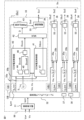
- FIG. 1 is a diagram showing a configuration of a power conversion device according to a first embodiment.
- FIG. 2 is a diagram showing a configuration of an inverter circuit in FIG. 1
- FIG. 3 is a diagram showing a first example of a transformer and a rectifier circuit in FIG. 1.
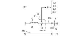
- FIGS. 4 to 6 are diagrams showing first to third examples of an inductor current output device in FIG. 1, respectively.
- FIG. 7 is a diagram showing a configuration of a control unit in FIG. 1
- FIG. 8 is a diagram showing an example of a hardware configuration that realizes the function of the control unit in FIG. 7 by digital calculation.
- FIG. 9 is a diagram showing an example of an output to each unit in a control signal in FIG. 1.
- FIG. 1 is a diagram showing a configuration of a power conversion device according to a first embodiment.
- FIG. 2 is a diagram showing a configuration of an inverter circuit in FIG. 1
- FIG. 3 is a diagram showing a first example of a
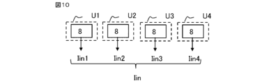
- FIG. 10 is a diagram explaining the sign of a phase input current output from each unit in FIG. 1
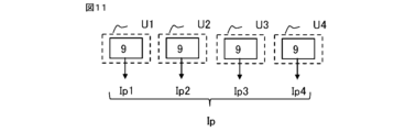
- FIG. 11 is a diagram explaining the sign of a primary side current output from each unit in FIG. 1.
- FIG. 12 is a diagram explaining the sign of an inductor current output from each unit in FIG. 1
- FIG. 13 is a diagram explaining the sign of a phase output current output from each unit in FIG. 1.
- FIG. 14 is a diagram explaining a duty ratio
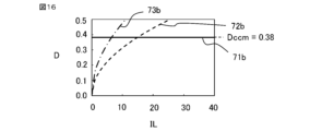
- FIGS. 15 and 16 are diagrams showing a first example and a second example of a duty ratio characteristic according to the first embodiment, respectively.
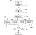
- FIG. 17 is a flowchart showing an example of a control method for a power conversion device according to the first embodiment.
- FIG. 18 is a flow chart showing a first example of step S05 in FIG.
- FIG. 17 is a flow chart showing a second example of step S05 in FIG. 17.
- FIG. 20 is a flow chart showing the processing steps of step S05 in FIG. 17.
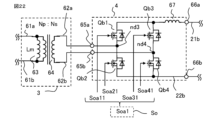
- FIGS. 21 to 23 are diagrams showing second to fourth examples of the transformer and rectifier circuit in FIG. 1, respectively.
- FIG. 24 is a diagram showing control signals output to the rectifier circuits in FIGS. 21 to 23.
- FIG. 25 is a diagram showing the configuration of control signals corresponding to FIGS. 21 and 23, and
- FIG. 26 is a diagram showing the configuration of control signals corresponding to FIG. 22.
- the power conversion device 100 of the first embodiment is a multi-phase power conversion device that includes a plurality of power conversion units U connected in parallel and a control unit 99 that controls the plurality of power conversion units U, and converts DC power input from input terminals 23a and 23b into DC power of a target voltage and outputs it from output terminals 24a and 24b.
- the DC power input to the power conversion device 100 is input from the DC source 19 through the input filter 17.
- the positive terminal (not shown) of the DC source 19 and the input terminal 23a of the power conversion device 100 are connected by the positive wiring 21a, and the negative terminal (not shown) of the DC source 19 and the input terminal 23b of the power conversion device 100 are connected by the negative wiring 22a.
- the input filter 17 is connected to the positive wiring 21a and the negative wiring 22a.
- the DC power output from the power conversion device 100 is supplied to the load 20 through the output filter 18.
- the output terminal 24a of the power conversion device 100 and the positive terminal (not shown) of the load 20 are connected by the positive wiring 21b, and the output terminal 24b of the power conversion device 100 and the negative terminal (not shown) of the load 20 are connected by the negative wiring 22b.
- FIG 1 an example is shown having four power conversion units U corresponding to four phases, i.e., phase 1 to phase 4.
- the power conversion device 100 shown in Figure 1 is an example where the number of phases is four.
- the reference symbols for the power conversion units will be collectively referred to as U, with U1 to U4 used when distinguishing between them.
- the power conversion units U corresponding to phase 1 to phase 4 are power conversion unit U1 to power conversion unit U4, respectively.
- power conversion units U1 to U4 corresponding to phase 1 to phase 4 will be simply referred to as power conversion units U1 to U4 of phase 1 to phase 4.
- a capacitor 7 is connected between the positive wiring 21b and the negative wiring 22b from the positive and negative junctions where the outputs of each power conversion unit U are joined to the output terminals 24a, 24b. That is, the positive and negative junctions where the outputs of the power conversion units U join are provided between the output terminals 27, 28 of the power conversion units U and the connection points with the positive and negative wirings 21b, 22b of the capacitor 7.
- the power conversion device 100 of the first embodiment converts the DC voltage of the DC source 19 into a desired target DC voltage and supplies it to the load 20.
- the DC source 19 is, for example, a battery, a DC power source and other battery systems such as solar cells, a power source that rectifies AC voltage to produce DC voltage, a DC power distribution network, etc.
- the load 20 is, for example, a DC load, an AC load via an inverter, etc.
- An AC load via an inverter is a device in which an inverter that converts DC voltage to AC voltage is connected to an AC load such as a motor that is powered by the inverter.
- the input filter 17 includes at least one of a smoothing capacitor, a normal mode filter, and a common mode filter.
- the output filter 18 includes at least one of a smoothing capacitor, a normal mode filter, and a common mode filter.
- the power conversion unit U will be described.
- the configuration of the power conversion unit U is shown in the power conversion unit U1 in FIG. 1.
- An example in which the power conversion units U2 to U4 have the same configuration will be described.
- the power conversion unit U is, for example, an isolated DC-DC converter including an inverter circuit 2, a transformer 3, a rectifier circuit 4, an inductor 5, and a capacitor 6 arranged in sequence from the input terminals 25 and 26 side.
- the inverter circuit 2 includes a plurality of switching elements that are PWM controlled, and the inductor 5 is arranged closer to the output terminals 24a and 24b than the plurality of switching elements.
- the power conversion unit U includes input terminals 25 and 26 to which DC power is input, and output terminals 27 and 28 to which the converted DC power of the target voltage is output.
- the input terminals 25 and 26 of each power conversion unit U are connected to the input terminals 23a and 23b of the power conversion device 100, respectively.
- the output terminals 27 and 28 of each power conversion unit U are connected to the output terminals 24a and 24b of the power conversion device 100, respectively.
- the positive wiring from the positive terminal of the DC source 19 to the inverter circuit 2 is indicated as 21a
- the negative wiring from the negative terminal of the DC source 19 to the inverter circuit 2 is indicated as 22a.
- the positive wiring from the positive terminal of the load 20 to the rectifier circuit 4 is indicated as 21b
- the negative wiring from the negative terminal of the load 20 to the rectifier circuit 4 is indicated as 22b.
- the inverter circuit 2 converts the input DC power into AC power
- the transformer 3 outputs AC power insulated from this AC power
- the rectifier circuit 4 converts the AC power output from the transformer 3 into DC power. Therefore, the primary side of the transformer 3 is connected to the output terminal (connection points nd1, nd2) of the inverter circuit 2, and the secondary side of the transformer 3 is connected to the input terminals 65a, 65b, and 65c of the rectifier circuit 4.
- the positive output terminal 66a of the rectifier circuit 4 is connected to the positive output terminal 27 of the power conversion unit U by the positive wiring 21b to which the inductor 5 is connected.
- the negative output terminal 66b of the rectifier circuit 4 and the negative output terminal 28 of the power conversion unit U are connected by the negative wiring 22b.
- the capacitor 6 is connected in parallel to the load 20 between the positive wiring 21b and the negative wiring 22b.
- the inverter circuit 2 includes switching elements Qa1 and Qa3 of the upper arm connected to the positive wiring 21a, and switching elements Qa2 and Qa4 of the lower arm connected to the negative wiring 22a, forming a full bridge circuit.
- the legs in which the upper arm and the lower arm are connected in series are a series body in which the switching elements Qa1 and Qa2 are connected in series, and a series body in which the switching elements Qa3 and Qa4 are connected in series.
- the connection point between the upper arm and the lower arm is connected to the AC wiring.
- the connection point nd1 between the switching elements Qa1 and Qa2 is connected to the AC wiring 61a.
- the connection point nd2 between the switching elements Qa3 and Qa4 is connected to the AC wiring 61b.
- FIG. 1 an example of a MOSFET (Metal Oxide Semiconductor Field Effect Transistor) having a transistor Tr and a diode Di is shown as the switching elements Qa1 to Qa4.
- the diode Di may be a parasitic diode of the MOSFET or a diode of a separate element.
- the drains d of the switching elements Qa1 and Qa3 are connected to the positive wiring 21a, and the sources s of the switching elements Qa2 and Qa4 are connected to the negative wiring 22a.
- the source s of the switching element Qa1 and the drain d of the switching element Qa2 are connected at the connection point nd1, and the source s of the switching element Qa3 and the drain d of the switching element Qa4 are connected at the connection point nd2.
- the cathode of the diode Di is connected to the drain d of the switching elements Qa1 to Qa4, and the anode of the diode Di is connected to the source s of the switching elements Qa1 to Qa4.
- a control signal So output from the control unit 99 is input to the gate g, which is the control terminal of the switching elements Qa1 to Qa4.
- control signal So1 a control signal corresponding to the power conversion unit U1, i.e., control signal So1
- the control signal So1 is input to the inverter circuit 2 of the power conversion unit U1
- the control signal So2 is input to the inverter circuit 2 of the power conversion unit U2
- the control signal So3 is input to the inverter circuit 2 of the power conversion unit U3
- the control signal So4 is input to the inverter circuit 2 of the power conversion unit U4.
- the control signals So11, So21, So31, and So41 are input to the gates g of the switching elements Qa1 to Qa4 in the power conversion unit U1, respectively.
- So is used collectively for the control signals, and So1, So2, So3, and So4 are used when distinguishing between them according to the power conversion unit U to which they are input. Furthermore, So11, So21, So31, and So41 are used when distinguishing between them according to the switching elements Qa1 to Qa4 of the power conversion unit U1 to which they are input. Similarly, as shown in FIG.
- the switching elements Qa1 to Qa4 are not limited to MOSFETs, and may be composed of, for example, an IGBT (Insulated Gate Bipolar Transistor) which is a transistor Tr and a diode Di connected in inverse parallel to the IGBT, or may be composed of a bipolar transistor.
- the semiconductor material of the switching elements Qa1 to Qa4 is not limited to Si (Silicon), and may be a wide band gap semiconductor material having a wider band gap than Si, such as silicon carbide (SiC), gallium nitride (GaN), or gallium oxide (Ga 2 O 3 ).
- the switching elements Qa1 to Qa4 may be Si-MOSFETs, Si-IGBTs, SiC-MOSFETs, SiC-IGBTs, GaN power transistors, Ga 2 O 3 power transistors, or the like.
- the switching elements Qa1 to Qa4 are IGBTs, the drain d and source s are replaced with collectors and emitters.
- the switching elements Qa1 to Qa4 are bipolar transistors such as GaN power transistors or Ga2O3 power transistors, the control terminal gate g is replaced with the base, and the drain d and source s are replaced with the collector and emitter.
- Switching elements Qa1 to Qa4 are symbolically represented as one, but they may be connected in multiple parallel or multiple series to increase the current capacity or withstand voltage. When connected in multiple parallel or multiple series, switching elements Qa1 to Qa4 may be configured as a mixture of the aforementioned Si-IGBTs, SiC-MOSFETs, etc.
- FIG. 3 A first example of the transformer 3 and the rectifier circuit 4 is shown in FIG. 3.
- the transformer 3 shown in FIG. 3 is a center tap type transformer.
- the transformer 3 has a primary winding 63 and a secondary winding 64.
- the primary winding 63 is connected between the AC wiring 61a and the AC wiring 61b.
- One end of the secondary winding 64 is connected to the input terminal 65a of the rectifier circuit 4 via the AC wiring 62a.
- the other end of the secondary winding 64 is connected to the input terminal 65b of the rectifier circuit 4 via the AC wiring 62b.
- the middle of the secondary winding 64 is connected to the input terminal 65c of the rectifier circuit 4 via the AC wiring 62c.
- the rectifier circuit 4 shown in FIG. 3 has two diodes Di.
- the anode of the first diode Di is connected to the input terminal 65a, and the cathode of the first diode Di is connected to the output terminal 66a.
- the anode of the second diode Di is connected to the input terminal 65b, and the cathode of the second diode Di is connected to the output terminal 66a.
- the input terminal 65c and the output terminal 66b of the rectifier circuit 4 are connected by the negative wiring 22b.
- the intermediate potential of the transformer 3 is the negative potential of the rectifier circuit 4.
- the windings of the primary winding 63 and the secondary winding 64 are Np and Ns, respectively.
- the transformer turns ratio n of the transformer 3 is Np/Ns.
- FIG. 4 Examples of the inductor 5 and capacitor 6 are shown in FIG. 4. As described above, one end of the inductor 5 is connected to the positive output terminal 66a of the rectifier circuit 4, and the other end is connected to one end of the capacitor 6 via the positive wiring 21b. The other end of the capacitor 6 is connected to the negative wiring 22b.
- the input information Sin is, for example, the input voltage Vin and input current Iint of the DC power input to the power conversion device 100, the output voltage Vo and output current Iot of the DC power output from the power conversion device 100, the phase input current Iin input to the power conversion unit U, the primary side current Ip of the transformer 3, the inductor current IL of the inductor 5, and the phase output current Io output from the power conversion unit U.
- the input voltage Vin is, for example, the output voltage of the DC source 19 detected by the voltage detector 14a.
- the input current Iint is, for example, the output current of the DC source 19 detected by the current detector 15a.
- the output voltage Vo is the voltage of the capacitor 7 detected by, for example, the voltage detector 14b.
- the output current Iot is the current output from the capacitor 7 detected by, for example, the current detector 15b.
- the phase input current Iin is the current in the positive wiring 21a connected to the inverter circuit 2 from the input terminal 25 detected by, for example, the current detector 8.
- the primary current Ip is the current in the AC wiring 61a detected by, for example, the current detector 9.
- the inductor current IL is the current of the inductor 5 output by, for example, the inductor current output device 12.
- the phase output current Io is the current in the positive wiring 21b from the capacitor 6 to the output terminal 27 detected by, for example, the current detector 13.
- the inductor current output device 12 outputs the inductor current IL, which is a detection or estimation of the current flowing through the inductor 5.
- First to third examples of the inductor current output device 12 are shown in Figures 4 to 6.
- the inductor current output device 12 shown in Figure 4 is an example of the current detector 10.
- the inductor current IL is the current in the positive wiring 21b up to the output side of the inductor 5, i.e., the connection point of the capacitor 6, detected by the current detector 10, which is the inductor current output device 12.
- the inductor current output device 12 shown in Figure 5 is an example of the first current estimation circuit 11.
- the inductor current IL is a current estimated based on the phase input current Iin or the primary side current Ip.
- the first current estimation circuit 11 estimates the inductor current IL by dividing the excitation current Im flowing through the excitation inductance Lm by the product of the detection value of the phase input current Iin or the primary side current Ip and the transformer turns ratio n of the transformer 3.
- the excitation current Im is calculated based on the excitation inductance Lm of the transformer 3, the input voltage Vin, and the duty ratio D of the control signal So, which will be described later.
- the inductor current output device 12 shown in FIG. 6 is an example of the second current estimation circuit 11 and the voltage detector 16.
- the inductor current IL is estimated by integrating the value of the inductor voltage VL of the inductor 5 detected by the voltage detector 16.
- phase input currents Iin1, Iin2, Iin3, and Iin4 are output from the current detectors 8 of the power conversion units U1, U2, U3, and U4, respectively.
- the signs of the phase input currents are collectively referred to as Iin, and when distinguishing between them by the power conversion unit U, Iin1, Iin2, Iin3, and Iin4 are used.
- primary side currents Ip1, Ip2, Ip3, and Ip4 are output from the current detectors 9 of the power conversion units U1, U2, U3, and U4, respectively.
- phase output currents Io1, Io2, Io3, and Io4 are output from the current detectors 13 of the power conversion units U1, U2, U3, and U4, respectively.
- the phase output current sign is collectively referred to as Io, and Io1, Io2, Io3, and Io4 are used when distinguishing between the power conversion units U.
- the control unit 99 includes a processor 50 such as a CPU (Central Processing Unit), a memory 51 for exchanging data with the processor 50, and an input/output interface for inputting and outputting signals between the processor 50 and the outside in order to control the power conversion units U1 to U4.
- the input/output interface includes an input circuit 52 for inputting signals between the processor 50 and the outside, and an output circuit 53 for outputting signals between the processor 50 and the outside.
- the processor 50 may include an ASIC (Application Specific Integrated Circuit), an IC (Integrated Circuit), a DSP (Digital Signal Processor), an FPGA (Field Programmable Gate Array), and various signal processing circuits.
- ASIC Application Specific Integrated Circuit
- IC Integrated Circuit
- DSP Digital Signal Processor
- FPGA Field Programmable Gate Array
- the processor 50 may include multiple devices of the same type or different types, and each process may be shared and executed.
- the memory 51 may be a RAM (Random Access Memory) configured to allow data to be read from and written to by the processor 50, or a ROM (Read Only Memory) configured to allow data to be read from the processor 50.
- the functions of the voltage control unit 31, phase shed control unit 32, and multiple current control units 33, which are functional blocks of the control unit 99 described below, are realized by the processor 50 and memory 51 shown in FIG. 8.
- the functional blocks of the control unit 99 are realized by the processor 50 executing a program stored in the memory 51.
- multiple processors 50 and multiple memories 51 may work together to execute each function.
- the input circuit 52 includes, for example, an AD (Analog-Digital) converter 54 that converts the analog signals of the phase input current Iin, primary current Ip, phase output current Io, and inductor current IL output from the current detectors 8, 9, and 13 and inductor current output device 12 provided in the power conversion units U1 to U4 into digital signals.
- the input circuit 52 also includes an AD converter 54 that converts the analog signals of the input voltage Vin, output voltage Vo, input current Iint, and output current Iot output from the voltage detectors 14a and 14b and current detectors 15a and 15b into digital signals. Note that only one AD converter 54 is shown in FIG. 8.
- the output circuit 53 includes a switching element drive circuit 55 that outputs a control signal So for driving the switching elements Qa1 to Qa4 of the power conversion units U1 to U4.
- the switching element drive circuit 55 outputs the digital signal control signal Sod with a changed voltage value. Note that the same symbols are used before and after AD conversion.
- the control unit 99 performs output voltage control of the power conversion device 100 and current control of the power conversion units U1 to U4 based on, for example, voltage information such as the input voltage Vin and output voltage Vo of the power conversion units U1 to U4, and current information of the power conversion units U1 to U4, i.e., input information Sin.
- the current used in the control described below may be the phase input currents Iin1 to Iin4 input to the inverter circuit 2, the primary side currents Ip1 to Ip4 of the transformer 3, or the inductor currents IL1 to IL4 of the inductor 5.
- overvoltages and overcurrents may be detected based on voltage and current information detected by the voltage detectors 14a and 14b and the current detectors 8, 9, 13, 15a and 15b, and the entire power conversion device 100 or at least one power conversion unit may be stopped and protected at a protection threshold.
- a temperature sensor may be provided to input temperature information, or protection may be provided by a threshold.
- the control unit 99 outputs a control signal So for driving the switching elements Qa1 to Qa4 of the power conversion units U1 to U4.
- the switching elements Qa1 to Qa4 are power semiconductor elements of the inverter circuit 2, and are arranged on the primary side of the transformer 3, so they are primary-side switching elements. An example in which the switching elements Qb1 to Qb4 are used in the rectifier circuit 4 of the power conversion units U1 to U4 (see Figures 21 to 23) will be described later.
- the control unit 99 also outputs a control signal So for driving the switching elements Qb1 to Qb4 of the power conversion units U1 to U4.
- the switching elements Qb1 to Qb4 are power semiconductor elements of the rectifier circuit 4, and are arranged on the secondary side of the transformer 3, so they are secondary-side switching elements.
- the control signal So is generated using a triangular wave comparison method such as PWM (Pulse Width Modulation) control.
- the secondary side switching elements Qb1 to Qb4 may be synchronously rectified to reduce the conduction loss of the diode forward voltage VF.
- the control unit 99 may be configured to shift the carrier phase of the triangular wave in order to control the power conversion units U1 to U4.
- the operation of shifting the phases of multiple power conversion units U to cancel the ripple of the output current Iot is called interleaving operation.
- interleaving operation By performing interleaving operation, it is possible to reduce the size of the input filter 17 and the output filter 18.
- interleaving There are various methods for interleaving, which can be realized by controlling the operation or stop of multiple power conversion units U.
- the four carrier phases may be shifted by approximately 45 degrees to operate.
- two carrier phases may be shifted by approximately 90 degrees to operate the four power conversion units U1 to U4 with two carrier phases.
- one of the four power conversion units U1 to U4 may be stopped and the three may be operated with the carrier phases shifted by approximately 60 degrees each. Also, two of the four power conversion units U1 to U4 may be stopped and two may be operated with the two carrier phases shifted by approximately 90 degrees.
- the aforementioned "approximately 45 degrees" refers to 40 degrees or more and 50 degrees or less, and preferably 44 degrees or more and 46 degrees or less. The same applies to phase angles with other values.
- the phase shift angle may be any phase shift that can suppress ripples in the output current Iot.
- a sawtooth wave carrier may be used instead of the triangular wave carrier used for PWM switching control.
- FIG. 7 shows the functional blocks in the control unit 99.
- the control unit 99 has a voltage control function, a phase number switching function, and a phase current control function.
- the control unit 99 has a current control unit 33 (33u1 to 33u4) for each phase, i.e., each power conversion unit U, a phase shedding control unit 32 having a current command generation unit 37 that generates a current command value for each phase and a stop signal generation unit 38 that generates a phase stop signal GB that stops the operation of each phase, and a voltage control unit 31 that generates an output current command value Iot*.
- the phase shedding control unit 32 outputs an inductor current command value IL** that tracks the inductor current IL for each power conversion unit U, so it can also be said to be a command control unit that outputs an inductor current command value IL**.
- the current control unit 33 generates a control signal So for each power conversion unit U that controls the corresponding multiple switching elements Qa1 to Qa4. In FIG.
- the inductor current command values IL1** to IL4** enclosed in long dashed squares are collectively represented by the inductor current command value IL**
- the phase stop signals GB1 to GB4 enclosed in dashed squares are collectively represented by the phase stop signal GB
- the inductor currents IL1 to IL4 enclosed in dashed circles are collectively represented by the inductor current IL.
- the voltage control unit 31 generates an output current command value Iot*, which is a command value for the output current Iot, based on the output voltage Vo and the output voltage command value Vo*.
- the voltage control unit 31 converts, for example, the error voltage between the output voltage command value Vo* and the detection value of the output voltage Vo, which is the voltage of the capacitor 7, into the current of the capacitor 7, i.e., the capacitor current, using a compensator, and calculates the total current command value for each phase, i.e., the output current command value Iot*, by adding the capacitor current and the value of the output current Iot detected by the current detector 15b.
- the compensator may be, for example, a P (Proportional) controller, a PI (Integral) controller, a PID (Proportional-Integral-Differential) controller, a Type-2 compensator, a Type-3 compensator, or any other controller that can adjust the gain characteristic or phase characteristic of the open loop characteristic.
- the phase shedding control unit 32 generates the current command value of each phase and the phase stop signal GB1 to GB4 from the total current command value of each phase, i.e., the output current command value Iot*.
- the inductor current command values IL1** to IL4** are used.
- the sign of the inductor current command value is collectively referred to as IL**, and when distinguishing according to the power conversion unit U, IL1**, IL2**, IL3**, and IL4** are used.
- the sign of the phase stop signal is collectively referred to as GB, and when distinguishing according to the power conversion unit U, GB1, GB2, GB3, and GB4 are used.
- the total current command value of each phase i.e., the output current command value Iot*, is equal to the sum of the inductor current command values IL1** to IL4** of each phase.
- the phase stop signal GB is turned on (enabled)
- the primary side switching elements Qa1 to Qa4 are turned off, i.e., the inverter circuit 2 is stopped.
- the secondary side switching elements Qb1 to Qb4 are turned off, i.e., the rectifier circuit 4 is stopped.
- the phase stop signal GB may be turned on when the current command value of each phase, i.e., the inductor current command value IL**, becomes equal to or less than a preset threshold, or when the total current command value, i.e., the output current command value Iot*, becomes equal to or less than a preset threshold.
- the threshold of the phase stop signal GB may be set to maximize the efficiency of the power conversion device 100, or to be less than the maximum temperature of the power conversion device 100, or to be set to an operating time that is closely related to the lifespan of the power conversion device 100.
- the current command value that is turned on i.e., the inductor current command value IL**
- the total current command value of each phase i.e., the output current command value Iot*
- the current control unit 33 includes a CCM current control unit (continuous current mode current control unit) 40, a DCM current control unit (discontinuous current mode current control unit) 41, a duty ratio selection unit 42, a PWM generation unit 43, and a switching element drive circuit 55.
- the digital calculation functions of the current control unit 33 are realized by the CCM current control unit 40, the DCM current control unit 41, the duty ratio selection unit 42, and the PWM generation unit 43.
- the reference number 33 is used collectively for the current control units, and 33u1, 33u2, 33u3, and 33u4 are used when distinguishing between them according to the power conversion unit U.
- the CCM current control unit 40 generates a duty ratio Dccm, which is a first duty ratio of the control signal So that controls the multiple switching elements Qa1 to Qa4 of the inverter circuit 2, based on the inductor current IL and the inductor current command value IL**, so as to flow the inductor current IL, which is a continuous current mode in which a current flows continuously through the inductor 5. Since the CCM current control unit 40 generates the first duty ratio (duty ratio Dccm) of the control signal So, it can also be called a first current control unit.
- the DCM current control unit 41 generates a duty ratio Ddcm, which is a second duty ratio of the control signal So that controls the multiple switching elements Qa1 to Qa4 of the inverter circuit 2, based on the inductor current command value IL**, so as to flow the inductor current IL, which is a discontinuous current mode in which a current flows intermittently through the inductor 5. Since the DCM current control unit 41 generates the second duty ratio (duty ratio Ddcm) of the control signal So, it can also be called a second current control unit.
- the duty ratio selection unit 42 selects one of the first duty ratio (duty ratio Dccm) and the second duty ratio (duty ratio Ddcm) corresponding to the current modes of the continuous current mode and the discontinuous current mode as the selected duty ratio, and determines the selected duty ratio as the duty ratio D of the control signal So.
- the duty ratio selection units 42 of the power conversion units U that continue to operate and the power conversion units U that start to operate determine the selected duty ratio.
- the selected duty ratio is the duty ratio D output from the duty ratio selection unit 42.
- FIG 14 shows the pulse of the control signal Sod, which is a digital signal.
- the duty ratio D is the high period Th during which the control signal Sod is at a high voltage (digital value 1), divided by the switching period Tsw of the control signal Sod.
- the duty ratio D is expressed as Th/Tsw.
- the duty ratio D of the control signal So which is a digital signal whose voltage value has been changed, is also expressed as Th/Tsw.
- the voltage control unit 31 generates an output current command value Iot*, which is a command value for the output current Iot in the DC power output from the output terminals 24a, 24b, using the output voltage command value Vo*, which is a command value for the target voltage, and the value of the output voltage Vo detected by the voltage detector 14a as the voltage of the DC power output from the output terminals 24a, 24b of the power conversion device 100.
- the PWM generation unit 43 generates a control signal Sod, which is a digital signal that controls the multiple switching elements Qa1 to Qa4 of the inverter circuit 2 by PWM control, based on the duty ratio D output from the duty ratio selection unit 42 and the phase stop signal GB output from the phase shedding control unit 32.
- the PWM generation unit 43 outputs a control signal Sod that stops the inverter circuit 2 when the phase stop signal GB is valid, i.e., indicates a stop, and does not output a control signal Sod that operates the inverter circuit 2 when the phase stop signal GB is invalid, i.e., indicates a non-stop.
- the switching element drive circuit 55 changes the voltage value of the input digital control signal Sod and outputs the digital control signal So with the changed voltage value.
- step S01 the control unit 99 acquires the output voltage command value Vo* (output voltage command value acquisition process).
- step S02 the control unit 99 acquires input information Sin (input information acquisition process).
- step S03 the control unit 99 calculates the output current command value Iot* by the voltage control unit 31 (output current command value calculation process).
- step S04 the control unit 99 calculates the inductor current command value IL** and the phase stop signal GB by the phase shedding control unit 32 (command calculation process).
- step S05 the control unit 99 executes a processing process for each power conversion unit U (power conversion unit processing process). After executing step S05, the control unit 99 ends the processing.
- FIG. 18 is a flowchart expanded to a first example of step S05
- FIG. 19 is a flowchart expanded to a second example of step S05.
- Step S05 shown in FIG. 18 is a case where multiple power conversion units U are processed in parallel
- step S05 shown in FIG. 19 is a case where multiple power conversion units U are processed sequentially.
- FIGS. 18 and 19 show a case where the number of power conversion units U is 4, i.e., the number of phases is 4.
- the power conversion unit processing step of step S05 includes steps S06a to S06d and step S07.
- step S06a the control unit 99 executes the processing step of power conversion unit U1 (first power conversion unit processing step).
- step S06b the control unit 99 executes the processing step of power conversion unit U2 (second power conversion unit processing step).
- step S06c the control unit 99 executes the processing step of power conversion unit U3 (third power conversion unit processing step).
- step S06d the control unit 99 executes the processing step of power conversion unit U4 (fourth power conversion unit processing step).
- step S07 the control unit 99 determines whether the processing steps of all power conversion units U have been completed, and continues with step S07 if there are any processing steps that have not yet been completed, and ends if the processing steps of all power conversion units U have been completed.
- the power conversion unit processing step of step S05 includes steps S06a to S06d.
- step S06a the control unit 99 executes the processing step for power conversion unit U1 (first power conversion unit processing step).
- step S06b the control unit 99 executes the processing step for power conversion unit U2 (second power conversion unit processing step).
- step S06c the control unit 99 executes the processing step for power conversion unit U3 (third power conversion unit processing step).
- step S06c in step S06d
- the control unit 99 executes the processing step for power conversion unit U4 (fourth power conversion unit processing step).
- step S06d the control unit 99 ends the processing.
- step S05 Specific processing of step S05 is shown in FIG. 20.
- the units Ux shown in FIG. 20 are power conversion units with x being the ordinal number of the power conversion units U.
- x is one of 1, 2, 3, and 4.
- the control unit 99 acquires the inductor current command value IL** and the phase stop signal GB of the power conversion unit Ux (command acquisition process).
- the control unit 99 acquires the input information Sin of the power conversion unit Ux (unit input information acquisition process).
- step S13 the control unit 99 generates the duty ratio Dccm, which is the first duty ratio, by the CCM current control unit 40 of the power conversion unit Ux, and prepares for control by the first duty ratio (first control process).
- the control unit 99 generates the duty ratio Ddcm, which is the second duty ratio, by the DCM current control unit 41 of the power conversion unit Ux, and prepares for control by the second duty ratio (second control process).
- step S15 the control unit 99 determines the current mode of the inductor current IL corresponding to the inductor current command value IL** in the command acquisition process (current mode determination process).
- the current mode determination process is performed based on the magnitude relationship between the duty ratio Dccm and the duty ratio Ddcm. Specifically, if Dccm ⁇ Ddcm, the current mode is determined to be continuous, and if Dccm>Ddcm, the current mode is determined to be discontinuous. If the current mode determination process determines that the current mode is continuous, the process proceeds to step S16, and if the current mode determination process determines that the current mode is discontinuous, the process proceeds to step S17.
- step S16 the control unit 99 sets the duty ratio Dccm to the duty ratio D by the duty ratio selection unit 42 (first duty ratio setting process).
- step S17 the control unit 99 sets the duty ratio Ddcm to the duty ratio D by the duty ratio selection unit 42 (second duty ratio setting process). Specifically, if Dccm ⁇ Ddcm, it is determined that the mode is continuous current mode, and the duty ratio Dccm is set to duty ratio D. If Dccm>Ddcm, it is determined that the mode is discontinuous current mode, and the duty ratio Ddcm is set to duty ratio D. In other words, a smaller duty ratio is set to duty ratio D.
- step S18 the control unit 99 determines the phase stop signal GB using the PWM generation unit 43 (stop signal determination process). Steps S15 to S17 are a duty ratio selection process.
- step S19 the control unit 99 outputs a control signal So that stops the power conversion unit Ux via the PWM generation unit 43 and the switching element drive circuit 55, and stops the power conversion unit Ux (power conversion unit stopping process).
- step S20 the PWM generation unit 43 and the switching element drive circuit 55 output a control signal So that operates the power conversion unit Ux, and drive the power conversion unit Ux with a duty ratio D (power conversion unit driving process).
- the CCM current control section 40 of the power conversion unit U includes a feedback controller 44 that calculates a feedback duty ratio Dccmb using a PI controller or the like to calculate the difference between the inductor current command value IL** and the detected inductor current IL, a feedforward controller 45 that calculates a feedforward duty ratio Dccmb using the output voltage Vo or the like, and an adder 46 that adds the feedback duty ratio Dccmb and the feedforward duty ratio Dccmf to generate a duty ratio Dccm for the current continuous mode.
- a P controller, PID controller, Type-2 compensator, Type-3 compensator, or any other controller that can adjust the gain or phase characteristics of the open loop characteristics may be used.
- the duty ratio Dccm for the current continuous mode when a PI controller is applied can be expressed by equation (1).
- IL** is the inductor current command value
- IL is the value of the inductor current
- Kp is the proportional gain of the PI controller
- Ki is the integral gain of the PI controller
- n is the turns ratio of the transformer
- Vin is the input voltage
- Vo is the output voltage.
- the CCM current control unit 40 When a PI controller is applied, the CCM current control unit 40 performs the calculation of equation (1), so the input voltage Vin is also input along with the output voltage Vo.
- the DCM current control section 41 of the power conversion unit U is equipped with a feedforward controller 47 that uses the inductor current command value IL**.
- the feedforward controller 47 generates a duty ratio Ddcm for the discontinuous current mode. Equation (7) can be used to determine the duty ratio Ddcm.
- the inductor current IL is reset to zero every control period, so that it is possible to freely control the input and output power of the power conversion device 100.
- the input power Pin in the power conversion unit U in the first embodiment in DCM can be expressed as shown in Equation (2).
- Fsw is the switching frequency, which can be expressed by equation (3) using the switching period Tsw of the switching elements Qa1 to Qa4.
- Fsw (1/Tsw)...(3)
- Vin is the input voltage
- Iin is the phase input current
- n is the transformer turns ratio of transformer 3
- Lf is the inductance of inductor 5 which is a smoothing inductor
- Vo is the output voltage
- Lm is the excitation inductance of transformer 3
- Da is the duty ratio.
- Da 2Ddcm.
- Equation (4) is solved for the duty ratio Da.
- the phase input current Iin can be approximated as shown in Equation (5). Iin ⁇ IL ⁇ Vo/Vin...(5)
- the inductor current IL of the phase i.e., the power conversion unit U
- the inductor current command value IL** it can be expressed as in equation (6).
- the phase output current Io may be converted into the inductor current command value IL**.
- the inductor current command value IL** is used instead of the value of the inductor current IL because the current average value of the inductor current IL cannot be sampled or estimated during DCM.
- the duty ratio Ddcm during DCM can be expressed as equation (7).
- Equation (7) shows that the degree of freedom for controlling the duty ratio Ddcm can be improved by the inductor current command value IL**, making it possible to control the power conversion unit U in a feedforward manner.
- the duty ratio Ddcm for the discontinuous current mode may be calculated using a table or the like, and the inductance Lf, excitation inductance Lm, and switching frequency Fsw may be varied according to the input voltage Vin, output voltage Vo, phase input current Iin, and phase output current Io.
- FIG. 15 and 16 show duty ratio characteristics 71a and 71b which are characteristics of the duty ratio Dccm in the continuous current mode, and duty ratio characteristics 72a and 72b which are characteristics of the duty ratio Ddcm in the discontinuous current mode.
- FIG. 15 and FIG. 16 show duty ratio characteristics 73a and 73b which are characteristics of the duty ratio Ddcm in the discontinuous current mode when the exciting inductance Lm is not taken into consideration.
- the horizontal axis is the inductor current IL
- the vertical axis is the duty ratio D.
- the difference between FIG. 15 and FIG. 16 is the difference in the duty ratio Dccm in the continuous current mode.
- the duty ratio Dccm shown in FIG. 15 and FIG. 16 is the feedforward duty ratio Dccmf
- the feedforward duty ratio Dccmf can be expressed by the formula (8).
- Dccmf nVo/2Vin...(8)
- FIG. 15 shows the case where the duty ratio Dccm is 0.27
- FIG. 16 shows the case where the duty ratio Dccm is 0.38.
- the transformer turns ratio n of the transformer 3 is 2, the input voltage Vin is 100 (arbitrary units), and the output voltage Vo is 27 (arbitrary units), the duty ratio Dccm is 0.27 from equation (8).
- the transformer turns ratio n of the transformer 3 is 2, the input voltage Vin is 100 (arbitrary units), and the output voltage Vo is 38 (arbitrary units), the duty ratio Dccm is 0.38 from equation (8). Therefore, the difference between FIG. 15 and FIG. 16 is also the difference in the input voltage Vin and the output voltage Vo. In both the continuous current mode and the discontinuous current mode, the optimal duty ratios Dccm and Ddcm also change as the input voltage Vin and the output voltage Vo change.
- the duty ratio Dccm in the continuous current mode is constant with respect to the inductor current IL, whereas the duty ratio Ddcm in the discontinuous current mode changes with the inductor current IL.
- the feedforward duty ratio Dccmf in the continuous current mode is given by equation (8), which is the equation enclosed by the parentheses () and () in equation (1) and is the equation to the right of the "+" on the right.
- the difference between the characteristics of the duty ratio Dccm and the duty ratio Ddcm is also clear from the equations for the feedforward duty ratio Dccmf in the continuous current mode and the duty ratio Ddcm in the discontinuous current mode. Since the discontinuous current mode occurs when the inductor current IL is low, it is sufficient to select the smaller of the duty ratio Dccm in the continuous current mode and the duty ratio Ddcm in the discontinuous current mode.
- the excitation inductance Lm is taken into account, resulting in duty ratio characteristics 72a and 72b, and the excitation inductance Lm is not taken into account, resulting in duty ratio characteristics 73a and 73b.
- the duty ratio Ddcm of the discontinuous current mode is larger when the excitation inductance Lm is not taken into account than when the excitation inductance Lm is taken into account.
- the control unit of the comparative example when the excitation inductance Lm is not taken into account may determine that the current mode is continuous current mode due to the magnitude relationship between the duty ratio Dccm and the duty ratio Ddcm.
- the mismatch of the current modes causes distortion of the output voltage Vo. Therefore, by taking the excitation inductance Lm into account, it is possible to further suppress the distortion of the output voltage Vo.
- the DCM current control unit 41 When the power conversion unit U does not use a transformer 3, there is no need to consider the excitation inductance Lm.
- the DCM current control unit 41 When the power conversion unit U uses a transformer 3, the DCM current control unit 41 generates a duty ratio Ddcm based on equation (8) that takes into account the excitation inductance Lm.
- the power conversion device 100 of embodiment 1 when the power conversion unit U uses a transformer 3 controls the power conversion unit U with a control signal So of a duty ratio D corresponding to the current modes of the continuous current mode and discontinuous current mode in the inductor current IL, so that it is possible to reduce output voltage distortion when switching the number of phases, which is the number of times the power conversion unit operates. Furthermore, the power conversion device 100 of embodiment 1 can achieve a high-speed control response without increasing the capacitance of the output-side capacitors 6 and 7.
- the number of power conversion units U connected in parallel is four, but the number of power conversion units U is not limited, and a configuration in which at least two or more power conversion units U are connected in parallel is also acceptable.
- the inputs may be connected in series and the outputs in parallel, or the inputs may be connected in series and the outputs in series, or the inputs may be connected in parallel and the outputs in series.
- the power conversion units U1 to U4 have the same configuration.
- the power conversion unit U is an isolated DC-DC converter, so the power conversion units U1 to U4 may each have a different configuration as long as they are isolated DC-DC converters.
- the capacitors 6 in phases 1 to 4 may be integrated into a configuration like capacitor Co.
- the inductor 5 may also be integrated into a configuration like a coupled inductor, for miniaturization.
- the inverter circuit 2 may be a half-bridge circuit or a three-phase circuit.
- the inverter circuit 2 may also be a multi-level system such as a three-level system, other than a two-level system.
- the switching elements Qb1 and Qb2 are the same as the switching element Qa1 and the like described above.
- One end of the secondary winding is connected to the input terminal 65a of the rectifier circuit 4 via AC wiring 62a.
- the other end of the secondary winding 64 is connected to the input terminal 65b of the rectifier circuit 4 via AC wiring 62b.
- the middle of the secondary winding 64 is connected to the input terminal 65c of the rectifier circuit 4 via AC wiring 62c.
- the drain d of the switching element Qb1 is connected to the input terminal 65a, and the source s of the switching element Qb1 is connected to the output terminal 66b.
- the drain d of the switching element Qb2 is connected to the input terminal 65b, and the source s of the switching element Qb2 is connected to the output terminal 66b.
- One end of the inductor 67 is connected to the input terminal 65c, and the other end of the inductor 67 is connected to the output terminal 66a.
- the output terminal 66a of the rectifier circuit 4 is connected to the outer positive side wiring 21b, and the output terminal 66b of the rectifier circuit 4 is connected to the outer negative side wiring 22b.
- the intermediate potential of the transformer 3 is the positive side potential of the rectifier circuit 4 via the inductor 67.
- the signs of the positive side wiring and negative side wiring inside the rectifier circuit 4 are the same as the signs of the positive side wiring and negative side wiring outside the rectifier circuit 4, 21b and 22b.
- the switching element drive circuit 55 of the current control unit 33 corresponding to the power conversion units U1 to U4 in the control unit 99 is provided with a first drive unit 56 and a second drive unit 57.
- the first drive unit 56 outputs a control signal So for the inverter circuit 2
- the second drive unit 57 outputs a control signal So for the rectifier circuit 4.
- control signal Soa1 is input to the rectifier circuit 4 of the power conversion unit U1
- control signal Soa2 is input to the rectifier circuit 4 of the power conversion unit U2
- control signal Soa3 is input to the rectifier circuit 4 of the power conversion unit U3
- the control signal Soa4 is input to the rectifier circuit 4 of the power conversion unit U4.
- Control signals Soa11 and Soa21 are input to the gates g of switching elements Qb1 and Qb2 in power conversion unit U1, respectively.
- the signs of the control signals input to rectifier circuit 4 are collectively referred to as So, and when distinguishing between them according to the power conversion unit U to which they are input, Soa1, Soa2, Soa3, and Soa4 are used.
- Soa11 and Soa21 are used (see Figure 25).
- Soa12 and Soa22 are used
- Soa13 and Soa23 are used
- Soa14 and Soa24 are used (see FIG. 25).
- the rectifier circuit 4 shown in FIG. 22 is an example equipped with four switching elements Qb1 to Qb4 and an inductor 67.
- the four switching elements Qb1 to Qb4 form a full bridge circuit.
- the transformer 3 in FIG. 22 differs from the transformer 3 in FIG. 3 and FIG. 21 in that the AC wiring 62c is not drawn out from the middle of the secondary winding 64.
- One end of the secondary winding 64 is connected to the input terminal 65a of the rectifier circuit 4 via the AC wiring 62a.
- the other end of the secondary winding 64 is connected to the input terminal 65b of the rectifier circuit 4 via the AC wiring 62b.
- the full bridge circuit composed of the four switching elements Qb1 to Qb4 has the same configuration as the inverter circuit 2 shown in FIG. 2.
- the switching elements Qb1 and Qb3 of the upper arm are connected to the positive side wiring 21b to which the inductor 67 is connected, and the switching elements Qb2 and Qb4 of the lower arm are connected to the negative side wiring 22b.
- the leg in which the upper arm and the lower arm are connected in series is a series body in which switching element Qb1 and switching element Qb2 are connected in series, and a series body in which switching element Qb3 and switching element Qb4 are connected in series.
- the connection point between the upper arm and the lower arm is connected to the AC wiring.
- the connection point nd3 between switching element Qb1 and switching element Qb2 is connected to the AC wiring 62a.
- the connection point nd4 between switching element Qb3 and switching element Qb4 is connected to the AC wiring 62b.
- FIG. 22 an example of MOSFETs having a transistor Tr and a diode Di is shown for the switching elements Qb1 to Qb4, similar to the switching elements Qa1 to Qa4.
- the drains d of the switching elements Qb1 and Qb3 are connected to the positive wiring 21b to which the inductor 67 is connected, and the sources s of the switching elements Qb2 and Qb4 are connected to the negative wiring 22b.
- the source s of the switching element Qb1 and the drain d of the switching element Qb2 are connected at the connection point nd3, and the source s of the switching element Qb3 and the drain d of the switching element Qb4 are connected at the connection point nd4.
- a control signal So output from the control unit 99 is input to the gates g, which are the control terminals of the switching elements Qb1 to Qb4.
- FIG. 22 shows an example in which a control signal So corresponding to the power conversion unit U1, i.e., control signal Soa1, is input.
- the second drive unit 57 of the switching element drive circuit 55 outputs a control signal So for the rectifier circuit 4.
- the control signal Soa1 is input to the rectifier circuit 4 of the power conversion unit U1
- the control signal Soa2 is input to the rectifier circuit 4 of the power conversion unit U2
- the control signal Soa3 is input to the rectifier circuit 4 of the power conversion unit U3
- the control signal Soa4 is input to the rectifier circuit 4 of the power conversion unit U4.
- Control signals Soa11, Soa21, Soa31, and Soa41 are input to the gates g of switching elements Qb1 to Qb4 in the power conversion unit U1, respectively.
- the signs of the control signals are as explained in the second example of the transformer 3 and rectifier circuit 4. However, since the number of switching elements in the rectifier circuit 4 has increased to four, the part relating to switching elements Qb1 to Qb4 is expanded.
- Soa11, Soa21, Soa31, and Soa41 are used (see Figure 26).
- the rectifier circuit 4 shown in FIG. 23 is an example equipped with two switching elements Qb1, Qb2 and two inductors 67a, 67b.
- the transformer 3 in FIG. 23 is the same as the transformer 3 in FIG. 22.
- One end of the inductors 67a, 67b is connected to the positive side wiring 21b
- the other end of the inductors 67a, 67b is connected to the drain d of the switching elements Qb1, Qb2, and the source s of the switching elements Qb1, Qb2 is connected to the negative side wiring 22b.
- connection point nd5 between the other end of the inductor 67a and the drain d of the switching element Qb1 is connected to the AC wiring 62a.
- connection point nd6 between the other end of the inductor 67b and the drain d of the switching element Qb2 is connected to the AC wiring 62b.
- the control signal So output from the control unit 99 is input to the gate g, which is the control terminal of the switching elements Qb1 and Qb2.
- the switching elements Qb1 to Qb4 are not limited to MOSFETs, and may be the switching elements described for the switching elements Qa1 to Qa4. By using wide band gap semiconductor materials for the switching elements Qb1 to Qb4, an inverter circuit with high voltage resistance, good heat dissipation, and high-speed switching is obtained. Although the switching elements Qb1 to Qb4 are symbolically shown as one, they may be connected in multiple parallel or multiple series to increase the current capacity or voltage resistance. When connected in multiple parallel or multiple series, the switching elements Qb1 to Qb4 may be configured as a mixture of the aforementioned Si-IGBTs, SiC-MOSFETs, etc.
- each power conversion unit U of the power conversion device 100 includes a transformer 3, but each power conversion unit U of the power conversion device 100 does not necessarily have to include a transformer 3.
- An example of a power conversion unit U that does not include a transformer 3 will be described.
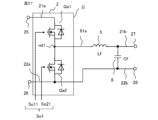
- Figure 27 is a diagram showing the configuration of another power conversion unit according to embodiment 1
- Figure 28 is a diagram showing the configuration of yet another power conversion unit according to embodiment 1.
- the power conversion unit U of Figure 27 and the power conversion unit U of Figure 28 include an inverter circuit 2, an inductor 5, and a capacitor 6.
- the inverter circuit 2 of Figure 27 includes switching elements Qa1 and Qa2 that form a half bridge.
- the inverter circuit 2 of Figure 28 includes switching elements Qa1 to Qa4 that form a full bridge.
- the inverter circuit 2 in FIG. 27 has the same configuration as the switching elements Qa1 and Qa2 in the inverter circuit 2 shown in FIG. 2.
- a connection point nd1 where the source s of the switching element Qa1 and the drain d of the switching element Qa2 are connected is connected to one end of the inductor 5 via an AC wiring 61a.
- the other end of the inductor 5 is connected to the output terminal 27 by a positive side wiring 21b.
- the inductor 5 and the capacitor 6 in FIG. 27 have the same configuration as the inductor 5 and the capacitor 6 in FIG. 4.
- the negative side wiring 22a connected to the input terminal 26 and the negative side wiring 22b connected to the output terminal 28 are connected to each other.
- the power conversion unit U in FIG. 27 outputs a DC output voltage Vo from the output terminals 27 and 28, which is stepped down from the DC input voltage Vin input from the input terminals 25 and 26.
- a connection point nd1 where the source s of the switching element Qa1 and the drain d of the switching element Qa2 are connected is connected to one end of the inductor 5 via the AC wiring 61a. The other end of the inductor 5 is connected to the output terminal 27 via the positive side wiring 21b.
- a connection point nd2 where the source s of the switching element Qa3 and the drain d of the switching element Qa4 are connected is connected to one end of the capacitor 6 via the AC wiring 61b.
- the AC wiring 61b and the negative side wiring 22b are connected to each other.
- the power conversion unit U of FIG. 28 has a configuration in which a half bridge of the switching elements Qa3 and Qa4 is added to the power conversion unit U of FIG. 27.
- the power conversion unit U in FIG. 28 can output a positive or negative output voltage Vo from the output terminals 27 and 28 by changing the potential of one end of the capacitor 6 connected to the output terminal 28 to either the positive side potential input from the input terminal 25 or the negative side potential input from the input terminal 26.
- the power conversion unit U in FIG. 28 can output a DC output voltage Vo boosted from the DC input voltage Vin input from the input terminals 25 and 26 from the output terminals 27 and 28.
- control of multiple power conversion units U by the control unit 99 may be PFM (Pulse Frequency Modulation) control, which controls frequency, rather than duty control by PWM control, or constant on-time (or constant off-time) control.
- PFM Pulse Frequency Modulation
- the pulse width of the control signals So1 to So4 output by the inverter circuit 2 arranged on the primary side of the transformer 3 may be controlled to output symmetrical pulses, or asymmetrical pulses may be output to perform soft switching, etc.
- the switching frequency Fsw is varied.
- PFM control the high period Th (see FIG. 14) of the pulse is kept constant and the switching frequency Fsw is changed.
- the duty ratio D of the PWM control is determined first and then the switching frequency Fsw is changed, in addition to PFM control.
- the feedforward duty ratio Dccmf of the above-mentioned formula (1) i.e., formula (8), uniquely determines the duty ratio Dccm by the input voltage Vin, the output voltage Vo, and the transformer turns ratio n.
- the output voltage Vo does not change even if the switching frequency Fsw changes, so there is no need to determine it for the purpose of controlling the output voltage Vo, but the switching frequency Fsw may be set to a value that minimizes the loss of the power conversion device 100, for example. That is, a switching frequency Fsw that minimizes the loss of the power conversion device 100 according to the input voltage Vin, the output voltage Vo, and the output power may be created as a table, and the switching frequency Fsw may be varied when the duty ratio Dccm is changed.
- the switching frequency Fsw may be varied so as to satisfy the above-mentioned formula (2). That is, even if the duty ratio Da or the switching frequency Fsw is changed, the input power Pin needs to remain the same.
- the formula (2) can be transformed into the formula (9).
- Equation (9) is in the form of multiplying the first equation Da ⁇ 2/Fsw by the remaining equations. For example, if the duty ratio Da has a lower limit Dmin and the duty ratio Da becomes smaller than the lower limit Dmin, it is necessary to change the switching frequency Fsw. Note that this lower limit Dmin is a lower limit set for a certain purpose, and the control unit 99 can also set it to a value less than the lower limit Dmin.
- the duty ratio D in the discontinuous current mode has a lower limit Dmin and if the duty ratio D becomes smaller than the lower limit Dmin, it is necessary to change the switching frequency Fsw.
- this lower limit Dmin is a lower limit set for a certain purpose, and the control unit 99 can also set it to a value less than the lower limit Dmin.
- the control unit 99 will be described when the switching frequency Fsw is varied in the control of multiple power conversion units U by the control unit 99.
- the control unit 99 has a switching frequency change unit 80 added to the current control unit 33 corresponding to each power conversion unit U.
- FIG. 29 shows the main part of the current control unit 33.
- FIG. 29 is a diagram showing the main part of another current control unit according to the first embodiment.
- the switching frequency change unit 80 includes a table switching frequency table 81 for selecting a switching frequency Fsw1 at which the loss of the power conversion device 100 is minimized according to the input voltage Vin, output voltage Vo, and output power in the current continuous mode, a switching frequency calculation unit 82 for calculating a switching frequency Fswa that keeps the input power Pin the same even if the duty ratio Da in the current discontinuous mode is changed, and a switching frequency output unit 83 for outputting a switching frequency Fswo, which is either the switching frequency Fsw1 or the switching frequency Fswa corresponding to the current continuous mode or the current discontinuous mode.
- the initial switching frequency input to the switching frequency change unit 80 is described as the switching frequency Fsw.
- the switching frequency change unit 80 In the case of the continuous current mode, the switching frequency change unit 80 outputs the switching frequency Fsw1 as the switching frequency Fswo. In the case of the discontinuous current mode, the switching frequency change unit 80 outputs the switching frequency Fswa as the switching frequency Fswo.
- the switching frequency Fswo is input to the PWM generation unit 43.
- the PWM generation unit 43 generates a digital control signal Sod that controls the multiple switching elements Qa1 to Qa4 of the inverter circuit 2 by PWM control based on the switching frequency Fswo, the duty ratio D selected by the duty ratio selection unit 42, and the phase stop signal GB.
- the switching element drive circuit 55 outputs a digital control signal So with a changed voltage value for the digital control signal Sod.
- the control signal So output from the current control unit 33 has a duty ratio D and switching frequency Fsw that correspond to the continuous current mode and discontinuous current mode.
- the power conversion device 100 of the first embodiment includes a plurality of power conversion units U connected in parallel, and a control unit 99 that controls the plurality of power conversion units U, converts DC power input from the input terminals 23a, 23b into DC power of a target voltage, and outputs it from the output terminals 24a, 24b.
- Each power conversion unit U includes a plurality of switching elements Qa1 to Qa4 that are PWM controlled, an inductor 5, and an inductor current output device 12 that outputs an inductor current IL that detects or estimates the current flowing through the inductor 5 that is arranged closer to the output terminals 24a, 24b than the plurality of switching elements Qa1 to Qa4.
- the control unit 99 includes a command control unit (phase shedding control unit 32) that outputs an inductor current command value IL** that tracks the inductor current IL for each power conversion unit U, and a current control unit 33 that generates a control signal So for each power conversion unit U to control the corresponding plurality of switching elements Qa1 to Qa4.
- a command control unit phase shedding control unit 32
- IL** inductor current command value
- a current control unit 33 that generates a control signal So for each power conversion unit U to control the corresponding plurality of switching elements Qa1 to Qa4.
- the current control unit 33 for each power conversion unit U includes a first current control unit (CCM current control unit 40) that generates a first duty ratio (duty ratio Dccm) of a control signal So that controls the multiple switching elements Qa1 to Qa4 to flow an inductor current IL that is a continuous current mode in which a current flows continuously through the inductor 5, based on an inductor current IL and an inductor current command value IL**; a second current control unit (DCM current control unit 41) that generates a second duty ratio (duty ratio Ddcm) of a control signal So that controls the multiple switching elements Qa1 to Qa4 to flow an inductor current IL that is a discontinuous current mode in which a current flows intermittently through the inductor 5, based on the inductor current command value IL**; and a duty ratio selection unit 42 that selects either the first duty ratio (duty ratio Dccm) or the second duty ratio (duty ratio Ddcm) corresponding to the current mode of the continuous current mode
- the power conversion device 100 of the first embodiment controls each parallel-connected power conversion unit U by a control signal So with a duty ratio D corresponding to the current modes of the continuous current mode and discontinuous current mode in the inductor current IL, thereby reducing output voltage distortion when switching the number of phases, which is the number of times the power conversion units U operate.
- the inductor current control method for the power conversion device of the first embodiment controls the inductor current IL, which is a current flowing through the inductor 5 in the power conversion device 100, which has an inductor 5 and is controlled by a control unit 99 and has multiple power conversion units U connected in parallel, converts DC power input from input terminals 23a, 23b into DC power of a target voltage, and outputs it from output terminals 24a, 24b.
- inductor current IL which is a current flowing through the inductor 5 in the power conversion device 100, which has an inductor 5 and is controlled by a control unit 99 and has multiple power conversion units U connected in parallel, converts DC power input from input terminals 23a, 23b into DC power of a target voltage, and outputs it from output terminals 24a, 24b.
- Each power conversion unit U includes multiple switching elements Qa1 to Qa4 that are PWM-controlled by a control signal So from the control unit 99, an inductor 5 arranged closer to the output terminals 24a, 24b than the multiple switching elements Qa1 to Qa4, and an inductor current output device 12 that outputs the detected or estimated inductor current IL.
- the inductor current control method for the power conversion device of the first embodiment includes a command output step, a first current control step, a second current control step, and a duty ratio selection step.
- the command output step outputs an inductor current command value IL** for each power conversion unit U, which causes the inductor current IL to follow.
- the first current control step generates, for each power conversion unit U, a first duty ratio (duty ratio Dccm) of a control signal So for controlling the multiple switching elements Qa1 to Qa4 to flow an inductor current IL that is a continuous current mode in which a current flows continuously through the inductor 5, based on an inductor current IL and an inductor current command value IL**.
- the second current control step generates, for each power conversion unit U, a second duty ratio (duty ratio Ddcm) of a control signal So for controlling the multiple switching elements Qa1 to Qa4 to flow an inductor current IL that is a discontinuous current mode in which a current flows intermittently through the inductor 5, based on an inductor current command value IL**.
- the duty ratio selection step selects, for each power conversion unit U, one of the first duty ratio (duty ratio Dccm) and the second duty ratio (duty ratio Ddcm) corresponding to the current mode of the continuous current mode and the discontinuous current mode as a selected duty ratio (duty ratio D), and determines the selected duty ratio (duty ratio D) as the duty ratio of the control signal So.
- each parallel-connected power conversion unit U is controlled by a control signal So with a duty ratio D corresponding to the current modes of the continuous current mode and discontinuous current mode in the inductor current IL, so that output voltage distortion can be reduced when switching the number of phases, which is the number of times the power conversion units U operate.
Landscapes
- Engineering & Computer Science (AREA)
- Power Engineering (AREA)
- Inverter Devices (AREA)
Priority Applications (2)
| Application Number | Priority Date | Filing Date | Title |
|---|---|---|---|
| PCT/JP2023/039448 WO2025094313A1 (ja) | 2023-11-01 | 2023-11-01 | 電力変換装置及び電力変換装置のインダクタ電流制御方法 |
| JP2025554425A JPWO2025094313A1 (https=) | 2023-11-01 | 2023-11-01 |
Applications Claiming Priority (1)
| Application Number | Priority Date | Filing Date | Title |
|---|---|---|---|
| PCT/JP2023/039448 WO2025094313A1 (ja) | 2023-11-01 | 2023-11-01 | 電力変換装置及び電力変換装置のインダクタ電流制御方法 |
Publications (1)
| Publication Number | Publication Date |
|---|---|
| WO2025094313A1 true WO2025094313A1 (ja) | 2025-05-08 |
Family
ID=95582567
Family Applications (1)
| Application Number | Title | Priority Date | Filing Date |
|---|---|---|---|
| PCT/JP2023/039448 Pending WO2025094313A1 (ja) | 2023-11-01 | 2023-11-01 | 電力変換装置及び電力変換装置のインダクタ電流制御方法 |
Country Status (2)
| Country | Link |
|---|---|
| JP (1) | JPWO2025094313A1 (https=) |
| WO (1) | WO2025094313A1 (https=) |
Citations (4)
| Publication number | Priority date | Publication date | Assignee | Title |
|---|---|---|---|---|
| JP2010517495A (ja) * | 2007-01-22 | 2010-05-20 | パワー・インテグレーションズ・インコーポレーテッド | カスケード結合されたpfcおよび共振モードパワーコンバータ |
| JP2011522505A (ja) * | 2008-05-14 | 2011-07-28 | ナショナル セミコンダクタ コーポレイション | 複数個のインテリジェントインバータからなるアレイ用のシステム及び方法 |
| US20190052169A1 (en) * | 2017-08-09 | 2019-02-14 | Microchip Technology Incorporated | Digital Control of Switched Boundary Mode Interleaved Power Converter |
| CN111740583A (zh) * | 2020-06-08 | 2020-10-02 | 南京航空航天大学 | 一种单周期控制在混合导通模式中的模态切换方法及电路 |
-
2023
- 2023-11-01 JP JP2025554425A patent/JPWO2025094313A1/ja active Pending
- 2023-11-01 WO PCT/JP2023/039448 patent/WO2025094313A1/ja active Pending
Patent Citations (4)
| Publication number | Priority date | Publication date | Assignee | Title |
|---|---|---|---|---|
| JP2010517495A (ja) * | 2007-01-22 | 2010-05-20 | パワー・インテグレーションズ・インコーポレーテッド | カスケード結合されたpfcおよび共振モードパワーコンバータ |
| JP2011522505A (ja) * | 2008-05-14 | 2011-07-28 | ナショナル セミコンダクタ コーポレイション | 複数個のインテリジェントインバータからなるアレイ用のシステム及び方法 |
| US20190052169A1 (en) * | 2017-08-09 | 2019-02-14 | Microchip Technology Incorporated | Digital Control of Switched Boundary Mode Interleaved Power Converter |
| CN111740583A (zh) * | 2020-06-08 | 2020-10-02 | 南京航空航天大学 | 一种单周期控制在混合导通模式中的模态切换方法及电路 |
Also Published As
| Publication number | Publication date |
|---|---|
| JPWO2025094313A1 (https=) | 2025-05-08 |
Similar Documents
| Publication | Publication Date | Title |
|---|---|---|
| US11909326B2 (en) | Parallel hybrid converter apparatus and method | |
| US11411502B2 (en) | Single-stage isolated DC-DC converters | |
| Mohr et al. | Converter systems for fuel cells in the medium power range—A comparative study | |
| US10199947B2 (en) | Isolated partial power processing power converters | |
| Vinnikov et al. | Step-up DC/DC converters with cascaded quasi-Z-source network | |
| US7110265B2 (en) | Non-isolated DC-DC converters with direct primary to load current | |
| CN100461601C (zh) | 一种实现隔离高频开关dc-dc变换的系统及方法 | |
| JP5866010B2 (ja) | 電力変換装置 | |
| JP5575235B2 (ja) | 電力変換装置 | |
| JP6367738B2 (ja) | 電力変換装置 | |
| US9595877B2 (en) | Secondary side hybrid converter apparatus and method | |
| US9806622B2 (en) | Power conversion device and power conversion control method for the same | |
| US10164546B2 (en) | Electric power conversion device | |
| WO2012014912A1 (ja) | Dc/dcコンバータ | |
| JP2016533704A (ja) | 高効率共振変換器のための装置および方法 | |
| JP2017169393A (ja) | Dc/dcコンバータの制御装置および制御方法 | |
| Ahmed | Modeling and simulation of ac–dc buck-boost converter fed dc motor with uniform PWM technique | |
| CN113489330A (zh) | 一种模块化整流结构谐振变换器的效率最优模态控制方法 | |
| Khan et al. | An overview of wide-voltage range isolated dc-dc converters | |
| JP6190979B2 (ja) | Dc/dcコンバータ | |
| WO2020129157A1 (ja) | 電力変換装置 | |
| JP6968361B2 (ja) | 電力変換回路及びその制御法 | |
| WO2025094313A1 (ja) | 電力変換装置及び電力変換装置のインダクタ電流制御方法 | |
| WO2025103591A1 (en) | Optimized asymmetric dc-dc converter | |
| JP2024034591A (ja) | 電源装置及び電源装置の制御方法 |
Legal Events
| Date | Code | Title | Description |
|---|---|---|---|
| 121 | Ep: the epo has been informed by wipo that ep was designated in this application |
Ref document number: 23957641 Country of ref document: EP Kind code of ref document: A1 |
|
| ENP | Entry into the national phase |
Ref document number: 2025554425 Country of ref document: JP Kind code of ref document: A |