WO2025089090A1 - 端子金具 - Google Patents
端子金具 Download PDFInfo
- Publication number
- WO2025089090A1 WO2025089090A1 PCT/JP2024/036238 JP2024036238W WO2025089090A1 WO 2025089090 A1 WO2025089090 A1 WO 2025089090A1 JP 2024036238 W JP2024036238 W JP 2024036238W WO 2025089090 A1 WO2025089090 A1 WO 2025089090A1
- Authority
- WO
- WIPO (PCT)
- Prior art keywords
- folded
- folded portion
- valley
- terminal fitting
- circuit board
- Prior art date
- Legal status (The legal status is an assumption and is not a legal conclusion. Google has not performed a legal analysis and makes no representation as to the accuracy of the status listed.)
- Pending
Links
Images


Classifications
-
- H—ELECTRICITY
- H01—ELECTRIC ELEMENTS
- H01R—ELECTRICALLY-CONDUCTIVE CONNECTIONS; STRUCTURAL ASSOCIATIONS OF A PLURALITY OF MUTUALLY-INSULATED ELECTRICAL CONNECTING ELEMENTS; COUPLING DEVICES; CURRENT COLLECTORS
- H01R12/00—Structural associations of a plurality of mutually-insulated electrical connecting elements, specially adapted for printed circuits, e.g. printed circuit boards [PCB], flat or ribbon cables, or like generally planar structures, e.g. terminal strips, terminal blocks; Coupling devices specially adapted for printed circuits, flat or ribbon cables, or like generally planar structures; Terminals specially adapted for contact with, or insertion into, printed circuits, flat or ribbon cables, or like generally planar structures
- H01R12/70—Coupling devices
- H01R12/71—Coupling devices for rigid printing circuits or like structures
-
- H—ELECTRICITY
- H01—ELECTRIC ELEMENTS
- H01R—ELECTRICALLY-CONDUCTIVE CONNECTIONS; STRUCTURAL ASSOCIATIONS OF A PLURALITY OF MUTUALLY-INSULATED ELECTRICAL CONNECTING ELEMENTS; COUPLING DEVICES; CURRENT COLLECTORS
- H01R13/00—Details of coupling devices of the kinds covered by groups H01R12/70 or H01R24/00 - H01R33/00
- H01R13/02—Contact members
- H01R13/03—Contact members characterised by the material, e.g. plating, or coating materials
Definitions
- This disclosure relates to terminal fittings.
- Patent Document 1 discloses a connector equipped with a fixing member having a board fixing portion that is fixed to a circuit board with solder.
- the fixing member of this connector is punched out with a die after plating the plate material (i.e., it is pre-plated).
- the cut surface cut by the die is not plated.
- Solder does not easily adhere to unplated parts.
- Patent Document 1 folds the board fixing portion so that the unplated area (i.e., the cut surface) is gathered in one place, thereby ensuring an area on the outer surface of the board fixing portion where solder can easily adhere.
- the cut surface is coated with plating by plating after punching out the plate material with a die (i.e., post-plating)
- the cut surface will be more likely to receive solder and spread.
- plating is performed after punching out the plate material with a die, it is necessary to perform plating while taking care not to deform or damage the fixing members after punching, which is time-consuming.
- the connector disclosed herein was developed based on the above circumstances, and aims to provide a terminal fitting that uses pre-plated sheet material and can be well connected to a circuit board using solder.
- the terminal fitting of the present disclosure is A terminal fitting made of a plate material having at least a part of its plate surface, excluding the cut surface, plated, a connection portion that is inserted into a through hole of a circuit board and fixed to the circuit board by soldering; a first folded portion extending from one of a pair of side edges of the connection portion parallel to an insertion direction into the through hole and folded back so as to overlap the connection portion; a second folded portion extending from the other of the pair of side edges and folded back so as to overlap the connection portion; Equipped with The cut surface of the extended end edge of the first folded portion and the cut surface of the extended end edge of the second folded portion face each other so as to abut against each other.
- pre-plated plate material can be used to achieve good connection to a circuit board using solder.
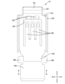
- FIG. 1 is a side cross-sectional view of a connector according to an embodiment.
- FIG. 2 is a plan view of the terminal fitting as viewed from above.
- FIG. 3 is a cross-sectional view taken along line AA in FIG.
- FIG. 4 is a cross-sectional view taken along line BB in FIG.
- FIG. 5 is a plan view of the connector as viewed from above.
- FIG. 6 is a perspective view showing a state in which the connection portion is connected to the circuit board by soldering.
- FIG. 7 is a cross-sectional view showing the configuration of a connection portion in another embodiment, in which the folded-back length of the first folded-back portion is made shorter than that of the second folded-back portion.
- FIG. 8 is a cross-sectional view showing the configuration of a connection portion in another embodiment, in which only the first folded portion is provided and folded back.
- a terminal fitting made of a plate material having at least a part of its plate surface, excluding the cut surface, plated, a connection portion that is inserted into a through hole of a circuit board and fixed to the circuit board by soldering; a first folded portion extending from one of a pair of side edges of the connection portion parallel to an insertion direction into the through hole and folded back so as to overlap the connection portion; a second folded portion extending from the other of the pair of side edges and folded back so as to overlap the connection portion; Equipped with The cut surface of the extended end edge of the first folded portion and the cut surface of the extended end edge of the second folded portion face each other so as to abut against each other.
- the terminal fitting (1) faces the first folded portion and the second folded portion so that the cut surfaces are butted against each other, so that the cut surfaces do not face the inner surface of the through hole in the circuit board. Therefore, even if the cut surfaces are not plated, the entire outer peripheral surface of the connection portion, the first folded portion, and the second folded portion that faces the inner surface of the through hole can be made into a plated surface to which solder can easily adhere and spread.
- a valley portion having a valley-shaped valley surface that becomes deeper toward the connection portion is formed on an outer surface of the extended end of the first folded portion and an outer surface of the extended end of the second folded portion,
- the valley surface is coated with plating, so that the solder adheres and spreads easily.
- the solder also wraps around the valley portion, and the solder adheres to the valley surface of the first folded portion and the valley surface of the second folded portion so that they rise toward each other, making it easier for the raised solder at the bottom of the valley portion to approach each other and join together. This makes it possible to adhere the solder so that it is connected to the outer surface of the first folded portion and the outer surface of the second folded portion, making it easier for the solder to spread.
- the terminal fitting (3) brings the extending ends of the first folded portion and the second folded portion closer together, making it easier to seamlessly connect the solder attached to the outer surface of the first folded portion and the solder attached to the outer surface of the second folded portion.
- FIG. 1 A first embodiment of a connector 1 having a terminal fitting 10 according to the present disclosure will be described with reference to Figs. 1 to 6.
- FIG. 1 A first embodiment of a connector 1 having a terminal fitting 10 according to the present disclosure will be described with reference to Figs. 1 to 6.
- “front”, “rear”, “upper”, “lower”, “right side”, and “left side” are represented by “F”, “B”, “U”, “D”, “R”, and “L”, respectively.
- the directional references are defined for convenience, and do not necessarily coincide with the directions when the connector 1 including the terminal fitting 10 is mounted on a vehicle or the like.
- the up-down direction is not limited to the direction of gravity.
- the connector 1 can connect the terminal fittings 10 housed in the housing 30 to the mating terminals 50 of a mating connector (not shown).
- the connector 1 has a pair of terminal fittings 10 and a housing 30.
- the connector 1 is attached to a circuit board S.
- the circuit board S is in the shape of a flat plate. Electronic components (not shown) are mounted on the upper and lower surfaces of the circuit board S. A pair of through holes H are formed penetrating the circuit board S in the plate thickness direction. A conductive portion La is provided on the lower surface of the circuit board S so as to surround the through holes H. A connection portion 10H of a terminal fitting 10 that is inserted into the through holes H and protrudes from the lower surface of the circuit board S is connected and fixed to the conductive portion La by soldering.
- the terminal fitting 10 is formed by pressing a metal plate, which is a conductive plate material.
- the terminal fitting 10 is a so-called female terminal fitting.
- the metal plate used for the terminal fitting 10 is plated before being pressed. That is, the metal plate is pre-plated. Therefore, in the terminal fitting 10 formed by pressing the metal plate, the cut surface 10S cut by the press working is not plated.
- the terminal fitting 10 is made of a plate material whose entire plate surface except for the cut surface 10S is plated.
- the pair of terminal fittings 10 have the same shape, and only differ in the position in which they are arranged. Therefore, the terminal fittings 10 will be described with reference to one of the terminal fittings 10. As shown in Figures 2 and 3, the terminal fitting 10 has a box portion 10A, multiple inclined portions 10C, multiple elastic contact portions 10D, multiple protrusions 10E, a spring portion 10G, and a connection portion 10H.
- the box portion 10A is in the shape of a rectangular tube, its axis is oriented in the vertical direction, and the upper and lower ends are open (see FIG. 3).
- the upper end of the box portion 10A is an insertion opening 10J into which the mating terminal 50 is inserted (see FIG. 3). That is, the box portion 10A has an insertion opening 10J into which the mating terminal 50 is inserted.
- the inclined portions 10C are provided one by one, connected to the upper ends of a pair of opposing walls of the box portion 10A (see FIG. 1). Each inclined portion 10C is connected to the opening edge (the opening edge at the upper end) of the insertion opening 10J and extends outward in the left-right direction and upward at an angle (see FIG. 1).
- the inclined portion 10C has a guide surface 10L that extends upward (forward in the opening direction of the insertion opening 10J) and connects to the opening edge, widening it so as to widen (see FIG. 1).
- the elastic contact portions 10D are formed in threes on the wall portion of the box portion 10A where the inclined portion 10C is connected. Each elastic contact portion 10D is a part of the wall portion, and is formed by cutting and raising the wall portion so as to protrude inward from the wall portion. Each elastic contact portion 10D is formed to extend upward in a cantilever shape (see FIG. 3). In other words, each elastic contact portion 10D has an elongated shape extending in the insertion and removal direction of the mating terminal 50. The elastic contact portion 10D can be elastically deformed to the inside and outside of the box portion 10A with the lower end as a base point. Each elastic contact portion 10D is arranged in a line in the circumferential direction of the box portion 10A.
- Each elastic contact portion 10D is formed to be inclined so as to protrude inward from the wall portion of the box portion 10A (see FIG. 1).
- the tip portion (upper end portion) of each elastic contact portion 10D is inclined outward in the left-right direction and upward (see FIG. 1).
- the protrusions 10E are formed in the box portion 10A so as to protrude inward, two at a time, from the wall portion on which the elastic contact portion 10D is arranged (see FIG. 2).
- Each protrusion 10E is a part of the wall portion, and is formed by hammering out the wall portion.
- the lower end of each protrusion 10E is flush with the upper end of the opening 10P that opens along the upper end of the elastic contact portion 10D (see FIG. 3).
- the protrusions 10E are formed on the edge of the opening 10P that is formed by cutting and raising the elastic contact portion 10D.
- the protrusions 10E are arranged in a position on the wall portion closer to the insertion opening 10J than the elastic contact portion 10D.
- the protrusions 10E are arranged in a line in the circumferential direction of the box portion 10A (see FIG. 2). Each protrusion 10E is formed so as to protrude inward from the wall portion of the box portion 10A (see FIG. 2). The upper part of each protrusion 10E is inclined downward toward the opposing wall portion (see FIG. 1). When the box portion 10A is viewed from above, each protrusion 10E is disposed so as to correspond to the space between adjacent elastic contact portions 10D (see FIG. 2). The distance between the protrusions 10E facing each other in the left-right direction is greater than the distance between the elastic contact portions 10D facing each other in the left-right direction (see FIG. 2).
- the spring portion 10G is formed in the box portion 10A, connected to the lower edge of one of the pair of walls on which the elastic contact portion 10D is formed.
- the spring portion 10G is formed in a band shape, and is formed in an S-shape extending in a direction away from the opposing wall portion of the box portion 10A (see Figure 1).
- the spring portion 10G has two bent portions 10M (see Figure 1).
- the spring portion 10G is positioned outside the box portion 10A (see Figure 2).
- a pair of locking pieces 10N are formed at the lower end of the spring portion 10G so as to protrude in the width direction.
- connection portion 10H is formed to be continuous with the lower end edge of the spring portion 10G and extend downward (see FIG. 1). As shown in FIG. 4, the connection portion 10H has a first folded portion 10Q and a second folded portion 10R.
- the first folded portion 10Q extends from one of a pair of side edges of the connection portion 10H parallel to the insertion direction (up-down direction) of the circuit board S into the through hole H, and is folded back so as to overlap the connection portion 10H.
- the second folded portion 10R extends from the other of a pair of side edges of the connection portion 10H parallel to the insertion direction of the circuit board S into the through hole H, and is folded back so as to overlap the connection portion 10H in the same direction as the first folded portion 10Q.
- the cut surfaces 10S of the extending edges of the first folded portion 10Q and the second folded portion 10R face each other so as to be butted together at a predetermined distance.
- the distance between the opposing cut surfaces 10S is smaller than the plate thickness dimension of the first folded portion 10Q and the second folded portion 10R.
- the cut surfaces 10S are not plated.
- a valley portion 10T is formed between the extending ends of the first folded portion 10Q and the second folded portion 10R.
- the valley portion 10T has a pair of valley surfaces 10U. These valley surfaces 10U are formed on the outer surfaces of the extending ends of the first folded portion 10Q and the second folded portion 10R in a valley shape that deepens toward the connecting portion 10H.
- these valley surfaces 10U are formed by a surface pressing process in which pressure is applied from the plate thickness direction during press processing. Therefore, the surface of each valley surface 10U is in a plated state.
- the housing 30 is made of synthetic resin. As shown in FIG. 1, the housing 30 is formed in a rectangular tubular shape extending in the vertical direction.
- the housing 30 has a partition wall 30A.
- the partition wall 30A is arranged to divide the space inside the housing 30 into a left side and a right side.
- Terminal fittings 10 are arranged in each of the left and right spaces inside the housing 30 divided by the partition wall 30A. These spaces are accommodation spaces A that accommodate the terminal fittings 10.
- An insertion hole 30B is formed in the upper end of the housing 30 corresponding to each accommodation space A.
- the lower part of the housing 30 is formed with a pair of protrusions 30C that protrude outward in the left-right direction so that the storage space A expands outward in the left-right direction.
- a pair of locking grooves 30D are formed within each of the protrusions 30C.
- the pair of locking grooves 30D are formed so as to extend upward from the lower end of each of a pair of walls whose plate thickness direction is oriented in a direction that intersects the left-right and up-down directions. Only one of the pair of locking grooves 30D is shown in Figure 1.
- the terminal fittings 10 are adjusted so that the connection parts 10H are lower than the box part 10A, and the terminal fittings 10 are accommodated in the accommodation spaces A from below the housing 30. At this time, the terminal fittings 10 are accommodated in the accommodation spaces A with the connection parts 10H of the terminal fittings 10 facing away from each other. Then, the locking pieces 10N are press-fitted into the locking grooves 30D of the housing 30 from below. In this way, the assembly of the housing 30 and the terminal fittings 10 is completed, and the connector 1 is completed.
- the insertion hole 30B of the housing 30 is formed so as to face the insertion port 10J, which is one opening of the box part 10A. Specifically, as shown in FIG. 5, when the connector 1 is viewed from above (opening direction), a part of the inner peripheral surface of the insertion hole 30B is located inside the outer peripheral surface of the box part 10A.
- the terminal fittings 10 are positioned away from the inner surface of the housing 30. In other words, the terminal fittings 10 are in a non-contact state with the housing 30, except for the locking piece 10N. Therefore, the box portion 10A of the terminal fitting 10 can swing left and right from the end of the spring portion 10G connected to the locking piece 10N as a base point within a range that does not contact the inner surface of the housing 30 (see Figure 1).
- connection portion 10H of the terminal fitting 10 is inserted into the through hole H of the circuit board S.
- the connection portion 10H is inserted into the through hole H from the upper surface side of the circuit board S.
- the connection portion 10H is connected and fixed to the conductive portion La of the circuit board S using solder. In this manner, the connector 1 is assembled to the circuit board S (see FIG. 1).
- connection portion 10H is connected and fixed to the conductive portion La of the circuit board S by solder being attached to the entire circumferential direction of the outer peripheral surface facing the inner surface of the through hole H.
- the solder is attached to the valley surface 10U of the first folded portion 10Q and rises up as it approaches the second folded portion 10R, and the solder is attached to the valley surface 10U of the second folded portion 10R and rises up as it approaches the first folded portion 10Q.
- the solder attached to the valley surface 10U of the first folded portion 10Q and the solder attached to the valley surface 10U of the second folded portion 10R are joined. In this way, the solder can be attached and spread so as to be smoothly continuous over the entire outer circumference of the connection portion 10H while maintaining the connection between the solder attached to the outer surface of the first folded portion 10Q and the outer surface of the second folded portion 10R.
- the terminal fitting 10 is made of a metal plate (sheet material) whose surface except for the cut surface 10S is plated.
- the terminal fitting 10 has a connection portion 10H that is inserted into a through hole H of a circuit board S and fixed to the circuit board S by soldering, a first folded portion 10Q that extends from one of a pair of side edges parallel to the insertion direction into the through hole H of the connection portion 10H and is folded back so as to overlap the connection portion 10H, and a second folded portion 10R that extends from the other of the pair of side edges and is folded back so as to overlap the connection portion 10H.
- the cut surface 10S of the extended edge of the first folded portion 10Q and the cut surface 10S of the extended edge of the second folded portion 10R face each other so as to be butted against each other.
- the cut surfaces 10S of the first folded portion 10Q and the second folded portion 10R are opposed to each other so that they are butted against each other, so that the cut surfaces 10S do not face the inner surface of the through hole H of the circuit board S. Therefore, even if the cut surfaces 10S are not plated, the entire outer peripheral surface of the connection portion 10H, the first folded portion 10Q, and the second folded portion 10R that faces the inner surface of the through hole H of the circuit board S can be made into a plated surface to which solder can easily adhere and spread.
- the outer surface of the extending end of the first folded portion 10Q and the outer surface of the extending end of the second folded portion 10R are formed with a valley portion 10T having a valley-shaped valley surface 10U that deepens toward the connecting portion 10H, and the surface of the valley surface 10U is plated.
- the valley surface 10U is coated with plating, so solder adheres and spreads easily.
- the solder also flows around the valley portion 10T, and the solder adheres to the valley surface 10U of the first folded portion 10Q and the valley surface 10U of the second folded portion 10R so that they rise toward each other, and the raised solder at the bottom of the valley portion 10T approaches each other and becomes easily joined, and as a result, the solder can be adhered to the outer surface of the first folded portion 10Q and the outer surface of the second folded portion 10R so that it is connected to them, making it easier for the solder to spread.
- the distance between the cut surface 10S of the extending end of the first folded portion 10Q and the cut surface 10S of the extending end of the second folded portion 10R is smaller than the plate thickness dimension of the first folded portion 10Q and the second folded portion 10R.
- connection part 110H shown in Fig. 7 the folded length of first folded part 110Q may be made shorter than that of second folded part 110R, thereby shifting the position of valley part 110T.
- connection part 210H shown in Fig. 8 only first folded part 210Q may be folded. In this case, it is considered that the extending end part of first folded part 210Q and the edge part of connection part 210H where the extending end part of first folded part 210Q is adjacent to each other may be subjected to surface pressing processing from the plate thickness direction.
- the number of inclined portions, the number of elastic contact portions, the number of protrusions, and the number of bent portions of the spring portion are not limited to those in the above embodiments.
- the spring portion may be bent in a Z-shape or crank shape.
- the distance between the cut surface of the extended end edge of the first folded portion and the cut surface of the extended end edge of the second folded portion may be greater than the plate thickness dimension of the first folded portion and the second folded portion.
- the terminal fittings may be male terminal fittings.
- a valley surface may be formed only on either the extending end of the first folded portion or the extending end of the second folded portion. Also, a configuration without a valley surface may be used.
- the terminal fitting may be made of a plate material in which only a portion of the plate surface, excluding the cut surface, is plated. Specifically, it is sufficient that the outer peripheral surface and valley surface of the connection portion, the first folded portion, and the second folded portion are plated.
- Connector 10 Terminal fitting 10A: Box portion 10C: Inclined portion 10D: Elastic contact portion 10E: Protrusion 10G: Spring portion 10H, 110H, 210H: Connection portion 10J: Insertion port 10L: Guide surface 10M: Bent portion 10N: Locking piece 10P: Opening 10Q, 110Q, 210Q: First folded portion 10R, 110R: Second folded portion 10S: Cut surface 10T, 110T: Valley portion 10U: Valley surface 30: Housing 30A: Partition wall 30B: Insertion hole 30C: Protrusion 30D: Locking groove 50: Counterpart terminal A: Storage space H: Through hole La: Conductive portion S: Circuit board
Landscapes
- Coupling Device And Connection With Printed Circuit (AREA)
Applications Claiming Priority (2)
| Application Number | Priority Date | Filing Date | Title |
|---|---|---|---|
| JP2023182932A JP2025072703A (ja) | 2023-10-25 | 2023-10-25 | 端子金具 |
| JP2023-182932 | 2023-10-25 |
Publications (1)
| Publication Number | Publication Date |
|---|---|
| WO2025089090A1 true WO2025089090A1 (ja) | 2025-05-01 |
Family
ID=95515696
Family Applications (1)
| Application Number | Title | Priority Date | Filing Date |
|---|---|---|---|
| PCT/JP2024/036238 Pending WO2025089090A1 (ja) | 2023-10-25 | 2024-10-10 | 端子金具 |
Country Status (2)
| Country | Link |
|---|---|
| JP (1) | JP2025072703A (https=) |
| WO (1) | WO2025089090A1 (https=) |
Citations (5)
| Publication number | Priority date | Publication date | Assignee | Title |
|---|---|---|---|---|
| JPH10106696A (ja) * | 1996-09-30 | 1998-04-24 | Sumitomo Wiring Syst Ltd | 基板用コネクタ及びその端子金具 |
| JP2001043914A (ja) * | 1999-07-28 | 2001-02-16 | Sumitomo Wiring Syst Ltd | 基板用コネクタ |
| JP2004200154A (ja) * | 2002-12-03 | 2004-07-15 | Sanyo Electric Co Ltd | 回路基板接続端子 |
| JP2008218187A (ja) * | 2007-03-05 | 2008-09-18 | Kobe Steel Ltd | Snめっき付き銅合金端子及びその製造方法 |
| JP2017103171A (ja) * | 2015-12-04 | 2017-06-08 | 住友電装株式会社 | 基板用コネクタ |
-
2023
- 2023-10-25 JP JP2023182932A patent/JP2025072703A/ja active Pending
-
2024
- 2024-10-10 WO PCT/JP2024/036238 patent/WO2025089090A1/ja active Pending
Patent Citations (5)
| Publication number | Priority date | Publication date | Assignee | Title |
|---|---|---|---|---|
| JPH10106696A (ja) * | 1996-09-30 | 1998-04-24 | Sumitomo Wiring Syst Ltd | 基板用コネクタ及びその端子金具 |
| JP2001043914A (ja) * | 1999-07-28 | 2001-02-16 | Sumitomo Wiring Syst Ltd | 基板用コネクタ |
| JP2004200154A (ja) * | 2002-12-03 | 2004-07-15 | Sanyo Electric Co Ltd | 回路基板接続端子 |
| JP2008218187A (ja) * | 2007-03-05 | 2008-09-18 | Kobe Steel Ltd | Snめっき付き銅合金端子及びその製造方法 |
| JP2017103171A (ja) * | 2015-12-04 | 2017-06-08 | 住友電装株式会社 | 基板用コネクタ |
Also Published As
| Publication number | Publication date |
|---|---|
| JP2025072703A (ja) | 2025-05-12 |
Similar Documents
| Publication | Publication Date | Title |
|---|---|---|
| JP2803574B2 (ja) | コネクタのプレスイン端子及びその製造方法 | |
| JP3202561B2 (ja) | 雄型端子金具 | |
| CN100438219C (zh) | 带加强接头片的电连接器 | |
| AU2006200182B2 (en) | Connector terminal fabrication process and connector terminal | |
| US7114253B2 (en) | Male terminal fitting and method of manufacturing the same | |
| US6322394B1 (en) | Electrical connector having a fixing mechanism and method for manufacturing said electrical connector | |
| US11088476B2 (en) | Board connector with chained terminals | |
| WO2025089089A1 (ja) | コネクタ | |
| US20040127097A1 (en) | Ground bus for an electrical connector | |
| JP3390721B2 (ja) | C形コンプライアントコンタクト | |
| KR19980702909A (ko) | 전기 리셉터클 어셈블리 및 그를 위한 스프링컨택트 | |
| JPH1040991A (ja) | コネクタ | |
| WO2025089090A1 (ja) | 端子金具 | |
| JP7060153B1 (ja) | コネクタ | |
| CN115136418B (zh) | 电接触元件 | |
| JP5786515B2 (ja) | コネクタ及びこのコネクタの組み立て方法 | |
| JP3886948B2 (ja) | 接続端子 | |
| CN112868141B (zh) | 连接器 | |
| JP7123561B2 (ja) | 電気接点 | |
| CN117855934A (zh) | 连接器壳体组件及usb插座 | |
| JP3067653B2 (ja) | コネクタ | |
| JPH0245305B2 (https=) | ||
| CN224204410U (zh) | 耳机插座连接器 | |
| CN218005309U (zh) | 端子和连接器 | |
| US20250149811A1 (en) | Connector |
Legal Events
| Date | Code | Title | Description |
|---|---|---|---|
| 121 | Ep: the epo has been informed by wipo that ep was designated in this application |
Ref document number: 24875749 Country of ref document: EP Kind code of ref document: A1 |