WO2025070623A1 - 接合用フィルム、半導体モジュール、インバータ、電子機器及び半導体モジュールの製造方法 - Google Patents
接合用フィルム、半導体モジュール、インバータ、電子機器及び半導体モジュールの製造方法 Download PDFInfo
- Publication number
- WO2025070623A1 WO2025070623A1 PCT/JP2024/034458 JP2024034458W WO2025070623A1 WO 2025070623 A1 WO2025070623 A1 WO 2025070623A1 JP 2024034458 W JP2024034458 W JP 2024034458W WO 2025070623 A1 WO2025070623 A1 WO 2025070623A1
- Authority
- WO
- WIPO (PCT)
- Prior art keywords
- metal
- bonding
- layer
- bonding film
- semiconductor module
- Prior art date
- Legal status (The legal status is an assumption and is not a legal conclusion. Google has not performed a legal analysis and makes no representation as to the accuracy of the status listed.)
- Pending
Links
Images

Classifications
-
- H—ELECTRICITY
- H10—SEMICONDUCTOR DEVICES; ELECTRIC SOLID-STATE DEVICES NOT OTHERWISE PROVIDED FOR
- H10W—GENERIC PACKAGES, INTERCONNECTIONS, CONNECTORS OR OTHER CONSTRUCTIONAL DETAILS OF DEVICES COVERED BY CLASS H10
- H10W40/00—Arrangements for thermal protection or thermal control
- H10W40/10—Arrangements for heating
-
- H—ELECTRICITY
- H10—SEMICONDUCTOR DEVICES; ELECTRIC SOLID-STATE DEVICES NOT OTHERWISE PROVIDED FOR
- H10W—GENERIC PACKAGES, INTERCONNECTIONS, CONNECTORS OR OTHER CONSTRUCTIONAL DETAILS OF DEVICES COVERED BY CLASS H10
- H10W72/00—Interconnections or connectors in packages
- H10W72/071—Connecting or disconnecting
Definitions
- the present invention relates to a bonding film, and a method for manufacturing a semiconductor module, inverter, electronic device, and semiconductor module using the same.
- TLPS transient liquid phase sintering
- a solder containing Sn is interposed between a first soldering base material containing Cu, which is the joining surface of a semiconductor chip element, and a second soldering base material containing Cu, which is the joining surface of a substrate, and heated at a temperature higher than the melting point of Sn, and the Cu contained in each soldering base material and the Sn contained in the solder are subjected to transition liquid phase sintering, thereby forming a connection layer containing an intermetallic compound copper-tin phase.
- connection layer for joining the semiconductor chip and substrate described in Patent Document 1 is a Cu-Sn intermetallic compound, which is a brittle material. Therefore, when the semiconductor chip and/or substrate are repeatedly heated and cooled, the stress caused by the difference in thermal expansion between the two cannot be fully alleviated, and cracks occur in the connection layer, running vertically from the substrate to the bonding layer. Furthermore, if this crack progresses from the substrate to the semiconductor chip element, it may damage the semiconductor chip element, which is an electronic component.
- Patent Document 2 discloses a joining sheet in which a coated rolled layer of paste containing Cu and Sn is provided on each side of a core sheet made of Cu or Al.
- This joining sheet is manufactured by applying a paste containing Cu and Sn to each side of a core sheet made of Cu or Al, drying it to form a dry layer, and then pressure-molding the dry layers formed on both sides of the core sheet and the core sheet together to provide a coated rolled layer of paste on each side of the core sheet.
- Patent Document 3 discloses a joint structure having a joint between a first member such as a semiconductor element and a second member such as a metal electrode or wiring, and the joint is made up of a bonding layer containing an intermetallic compound of a first metal of Ni or Cu and a second metal of Sn, and a buffer layer made of Al or an Al alloy and having a notch.
- the buffer layer has a notch for inducing cracks into the buffer layer, which induces the occurrence of cracks in the buffer layer and inhibits the occurrence and progression of cracks near the joint.
- the present invention aims to provide a bonding film that prevents cracks caused by internal thermal strain stress and exhibits good dicing performance, as well as a method for manufacturing a semiconductor module, inverter, electronic device, and semiconductor module that use the same.
- the bonding film according to the embodiment of the present invention includes a metal layer, a first bonding layer provided on one surface of the metal layer, and a second bonding layer provided on the other surface of the metal layer,
- the metal layer includes a metal having a thermal conductivity of 100 W/m ⁇ K or more at a temperature of 300 K,
- the metal layer has a 0.2% yield strength of 250 MPa or less.
- a semiconductor module includes the bonding film, a first bonded material bonded to the first bonding layer, and a second bonded material bonded to the second bonding layer,
- the first material to be joined is an electronic component
- the second material to be joined is a metal substrate or a metal lead frame.
- An inverter according to an embodiment of the present invention is equipped with the semiconductor module.
- the electronic device is equipped with the inverter.
- the method for manufacturing a semiconductor module includes a step of bonding the electronic component to the metal substrate or metal lead frame via the bonding film by heating the electronic component to the metal substrate or metal lead frame for 1 to 20 minutes at a temperature of 230°C to 350°C in an inert or reducing atmosphere with the bonding film interposed between the electronic component and the metal substrate or metal lead frame.
- the present invention provides a bonding film that prevents cracks caused by internal thermal strain stress and exhibits good dicing performance, as well as a semiconductor module, inverter, electronic device, and method for manufacturing a semiconductor module that uses the same.
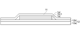
- FIG. 1 is a schematic cross-sectional view showing an example of a dicing/die bonding film using the bonding film of the present invention.
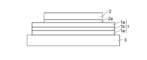
- FIG. 2 is a schematic cross-sectional view showing an example of a semiconductor module produced using the bonding film of the present invention.
- FIG. 3 is a schematic cross-sectional view showing a mounting sample of a semiconductor module produced using the bonding film of Comparative Example 1. As shown in FIG.
- the bonding film according to the present invention includes a metal layer, a first bonding layer provided on one surface of the metal layer, and a second bonding layer provided on the other surface of the metal layer. That is, the bonding film has a multilayer structure in which the metal layer is provided between the first bonding layer and the second bonding layer, and the metal layer is arranged as a stress relaxation intermediate layer.
- the first bonding layer is provided to be bonded to a first bonded material described later as one bonding surface of the bonding film
- the second bonding layer is provided to be bonded to a second bonded material described later as one bonding surface of the bonding film.
- the bonding film functions as a bonding material that bonds the first bonded material and the second bonded material. Since a metal layer having a predetermined property is inserted as an intermediate layer of the bonding film, when a semiconductor module is produced in which the bonding film is bonded to each of the bonded materials having different linear expansion coefficients, such as a silicon semiconductor chip element and a copper substrate, even if heat is applied to the bonding film, the thermal strain stress applied to the inside of the bonding film due to the difference in linear thermal expansion of each of the bonded materials, such as the semiconductor chip element and the copper substrate, is absorbed by the elastic deformation or plastic deformation of the metal layer. As a result, it is possible to prevent the occurrence of cracks inside the bonding film and suppress a decrease in the lifespan of the elements and an increase in thermal resistance.
- the metal layer contains a metal having a thermal conductivity of 100 W/m ⁇ K or more at a temperature of 300 K. This makes it easier to establish a thermal conduction and electrical conduction path than in a structure in which the bonding layer is a single layer, and also improves the thermal conductivity and electrical conductivity of the bonding film.
- metals include copper (Cu), zinc (Zn), aluminum (Al), silver (Ag), gold (Au), magnesium (Mg), aluminum alloys, copper alloys, and zinc alloys, and copper (Cu), zinc (Zn), aluminum (Al), aluminum alloys, copper alloys, or zinc alloys are preferred, and copper (Cu), zinc (Zn), or aluminum (Al) are more preferred.
- the metal layer has a 0.2% yield strength of 250 MPa or less.
- the 0.2% yield strength of the metal layer is preferably 250 MPa or less, more preferably 120 MPa or less, and even more preferably 50 MPa or less.
- the lower limit of the 0.2% yield strength is preferably 5 MPa or more in order to impart a certain deformation resistance to the metal layer as well (to impart a certain deformation resistance and ensure handling during manufacturing).
- the shape of the metal layer is, for example, foil-like, mesh-like, fibrous, pellet-like, etc., and is preferably foil-like.
- the metal layer may be a metal foil that has been perforated or unevenly processed. By using such a metal foil that has been subjected to various processes, the deformation resistance of the metal layer, such as elastic deformation and plastic deformation, is reduced, so that the 0.2% yield strength can be lowered.
- the metal layer may be a metal foil that has been softened in advance by heat treatment.
- the heating temperature is preferably 200°C to 700°C, and more preferably 400°C to 600°C.
- the heating time is preferably 1 minute to 90 minutes, and more preferably 30 minutes to 60 minutes.
- the metal foil may be both softened by heat treatment and perforated or unevenly processed.
- the porosity is preferably 5% to 70% and more preferably 15% to 55% relative to one surface of the metal foil.
- an porosity of 30% to 45% reduces the 0.2% yield strength of the metal layer, improving dicing performance and not significantly impairing thermal conductivity.
- the metal layer is more likely to undergo elastic or plastic deformation, making it easier to prevent cracks caused by thermal distortion stress applied to the inside of the bonding film, and improving reliability in application under high temperature operation.
- the width (diameter) of the opening is not particularly limited, but is preferably 0.05 mm to 5 mm and more preferably 0.1 mm to 0.5 mm.
- the thickness of the metal layer is preferably 8 ⁇ m or more and 200 ⁇ m or less, and more preferably 9 ⁇ m or more and 100 ⁇ m or less.
- the bonding film becomes easier to process, improving dicing performance. It is also effective for use as a bonding film for smaller semiconductor modules.
- a first bonding layer and a second bonding layer are provided on both sides of the metal layer.
- the first bonding layer and the second bonding layer each preferably contain at least one type of metal particle (P) as a metal component.
- the materials of the first bonding layer and the second bonding layer, i.e., the metal particles (P) contained in the first bonding layer and the second bonding layer, may be the same or different, but from the viewpoint of productivity, connectivity with the metal layer, etc., it is preferable that they are all the same.
- the first bonding layer and the second bonding layer are preferably paste layers formed using a paste-like conductive composition.
- a conductive composition contains at least one type of metal particles (P), a thermosetting resin, a flux, and a solvent, and may further contain various additives as necessary.
- the first bonding layer and the second bonding layer are produced by forming a coating film by applying such a paste-like conductive composition and drying the coating film.
- the metal particles (P) as the metal component preferably contain, for example, first metal particles (P1) made of one metal selected from the group consisting of copper (Cu), nickel (Ni), silver (Ag) and gold (Au) or an alloy containing two or more metals selected from these groups.
- first metal particles (P1) are suitable as metal particles (P) of the conductive composition described below because of their excellent electrical conductivity and thermal conductivity, and are particularly preferably Cu particles or alloy particles containing Cu, which are inexpensive and have excellent thermal conductivity.
- the metal particles (P) may further include second metal particles (P2) having a metal element different from the first metal particles (P1).
- the metal particles (P) include the first metal particles (P1) and the second metal particles (P2), and it is preferable that the first metal particles (P1) and the second metal particles (P2) each contain a metal component capable of forming an intermetallic compound with each other. Since the first metal particles (P1) and the second metal particles (P2) each contain a metal capable of forming an intermetallic compound with each other, the metal particles (P) as a whole are a low melting point metal or alloy in an unsintered state, but can form a high melting point intermetallic compound after sintering. As a result, such metal particles can achieve a lower mounting temperature, while exhibiting excellent heat resistance without performance degradation even at temperatures above the mounting temperature after sintering.
- the second metal particles (P2) may contain a metal element different from the first metal particles (P1) and capable of forming an intermetallic compound with the first metal particles (P1).
- second metal particles (P2) are preferably made of one metal selected from the group consisting of aluminum (Al), tin (Sn), zinc (Zn), titanium (Ti), indium (In), bismuth (Bi), gallium (Ga) and palladium (Pd) or an alloy containing two or more metals selected from this group.
- the first metal particles (P1) are Cu particles
- the second metal particles (P2) are preferably metal particles capable of forming an intermetallic compound with Cu, such as Sn particles or alloy particles containing Sn.
- the combination of the first metal particles (P1) and the second metal particles (P2) capable of forming such an intermetallic compound can be appropriately selected, but it is preferable that intermetallic compounds such as Cu-Sn, Ni-Sn, Ag-Sn, Cu-Zn, Ni-Zn, and Ni-Ti can be formed, and when it is necessary to set the mounting temperature as low as possible, it is preferable that the second metal particles (P2) contain Sn, which has a low melting point, and in particular, a Cu-Sn combination is more preferable.
- the first metal particles (P1) are Cu particles
- the second metal particles (P2) are Sn particles or Sn-based solder particles.
- the content of the first metal particles (P1) in each of the first bonding layer and the second bonding layer is preferably 59 mass% or less, more preferably 58 mass% or less, and even more preferably 57 mass% or less.
- the lower limit of the content of the first metal particles (P1) is preferably 54 mass% or more, and more preferably 56 mass% or more.
- the content of the second metal particles (P2) in each of the first bonding layer and the second bonding layer is preferably 32% by mass or more and 41% by mass or less, and more preferably 35% by mass or more and 37% by mass or less.
- the metal components are substantially free of Pb (lead), Hg (mercury), Ab (antimony) and As (arsenic), and the total content of these metals in the entire metal components is preferably less than 0.1% by mass.
- the shape of the metal particles (P) is not particularly limited, and spherical particles, dendritic particles, scale-like particles, spike-like particles, etc. can be used as appropriate.
- the particle size of the metal particles (P) is also not particularly limited, but the average particle size (D50) of the first metal particles (P1) is preferably 15 ⁇ m or less, and the average particle size (D50) of the second metal particles (P2) is more preferably 15 ⁇ m or less.
- the average particle size (D50) is a value calculated based on measurement by a laser diffraction scattering type particle size distribution measurement method.
- the content of the metal components in the conductive composition is preferably 70 to 96% by mass, and more preferably 80 to 94% by mass.
- the conductive composition contains at least one thermosetting resin as a binder component.
- thermosetting resin as a binder component.
- the inclusion of the thermosetting resin in the conductive composition contributes to film properties (ease of molding, ease of handling, etc.) in an unsintered state, and after sintering, the stress generated between the bonding material described below, for example, electronic components such as semiconductor elements, and metal substrates, metal lead frames, etc., due to a heat cycle can be alleviated.
- the thermosetting resin preferably contains a maleic acid imide compound containing two or more imide group units per molecule, particularly from the viewpoint of heat resistance and film properties when mixed with metal particles (P).
- a resin containing a maleic acid imide compound containing two or more imide group units per molecule is maleic acid imide resin (hereinafter sometimes referred to as "maleimide resin").
- maleimide resin maleic acid imide resin
- the thermosetting resin containing the maleic acid imide resin has excellent stress relaxation properties, and therefore can improve the thermal fatigue resistance properties of the conductive composition after sintering.
- the maleic acid imide resin can be obtained, for example, by condensing maleic acid or its anhydride with a diamine or polyamine. From the viewpoint of stress relaxation, it is preferable that the maleic acid imide resin contains a skeleton derived from an aliphatic amine having 10 or more carbon atoms, and it is particularly preferable that the skeleton has 30 or more carbon atoms and is represented by the following structural formula (1). It is also preferable that the number average molecular weight of the maleic acid imide resin is 3000 or more.
- the molecular weight and glass transition temperature Tg of the maleic acid imide resin may be adjusted by including a skeleton derived from an acid component other than maleic acid, such as benzenetetracarboxylic acid or its anhydride, or hydroxyphthalic acid bisether or its anhydride.
- maleimide resins for example, bismaleimide resins shown in the following structural formulas (2) to (4) are preferably used.
- n is an integer from 1 to 10.
- the portion “X” is "C 36 H 72 " represented by the following structural formula (6).
- "*" indicates the bonding site with N.
- the content of the thermosetting resin contained in the conductive composition is preferably 4% by mass or more and 30% by mass or less, and more preferably 6% by mass or more and 20% by mass or less.
- the thermosetting resin may be one type of thermosetting resin alone, or two or more types of thermosetting resins may be used in combination.
- the conductive composition may further contain a thermosetting resin other than the above, such as a phenolic resin, novolac (phenol and/or cresol), polyurethane resin, polyimide resin, cyanate ester resin, polyvinyl alcohol resin, polyester resin, polyurea resin, benzoxazine resin, acrylate resin, cyanate ester resin, and/or a combination thereof.
- the conductive composition may further contain a flux having one or more phosphorus or sulfur in its molecular structure that can bond with oxygen atoms without generating water.
- the flux has a function of removing the oxide film on the surface of the metal particles (P) contained in the conductive composition, and is particularly effective on metals that are easily oxidized such as copper, tin, nickel and aluminum.
- organic phosphines, sulfide compounds and thiol compounds are preferred, and these compounds are extremely difficult to absorb moisture and have excellent moisture absorption resistance compared to fluxes such as carboxylic acids and alcohols that have been commonly used in the past.
- the flux preferably contains at least one of the organic phosphines represented by the following general formula (6), the sulfide-based compound represented by the following general formula (7), and the thiol-based compound represented by the following general formula (8).
- R in the following general formulas (6) and (7) each independently represents an organic group and may be the same or different.
- each R is preferably independently selected from an alkyl group, an aryl group, an organic group having a functional group, an organic group having a heteroatom, and an organic group having an unsaturated bond, and at least one R is preferably an aryl group.
- the alkyl group may be linear, branched, or cyclic, and may have a substituent.
- the alkyl group is preferably linear or branched.
- the alkyl group preferably has 3 or more carbon atoms, more preferably has 4 to 18 carbon atoms, and even more preferably has 6 to 15 carbon atoms.
- Examples of such alkyl groups include propyl, butyl, pentyl, hexyl, heptyl, octyl, nonyl, decyl, stearyl, and isostearyl groups.
- the aryl group may have a substituent and preferably has 6 to 10 carbon atoms.
- Examples of such aryl groups include a phenyl group, a tolyl group, a xylyl group, a cumenyl group, and a 1-naphthyl group.
- the organic group having a functional group preferably has 1 to 10 carbon atoms, more preferably 1 to 6 carbon atoms, and even more preferably 1 to 3 carbon atoms.
- the functional group include halogen groups such as a chloro group, a bromo group, and a fluoro group.
- organic groups having such functional groups include a chloroethyl group, a fluoroethyl group, a chloropropyl group, a dichloropropyl group, a fluoropropyl group, a difluoropropyl group, a chlorophenyl group, and a fluorophenyl group.
- the organic group having a heteroatom preferably has 1 or more carbon atoms, more preferably has 4 to 18 carbon atoms, and even more preferably has 6 to 15 carbon atoms.
- heteroatoms include nitrogen atoms, oxygen atoms, and sulfur atoms.
- organic groups having such heteroatoms include dimethylamino groups, diethylamino groups, diphenylamino groups, methyl sulfoxide groups, ethyl sulfoxide groups, and phenyl sulfoxide groups.
- the organic group having an unsaturated bond preferably has 3 or more carbon atoms, more preferably has 4 to 18 carbon atoms, and even more preferably has 6 to 15 carbon atoms.
- Examples of organic groups having such unsaturated bonds include propenyl groups, propynyl groups, butenyl groups, butynyl groups, oleyl groups, phenyl groups, vinylphenyl groups, and alkylphenyl groups, and among these, vinylphenyl groups are preferred.
- each R independently has at least one selected from the group consisting of vinyl groups, acrylic groups, methacrylic groups, maleic acid ester groups, maleic acid amide groups, maleic acid imide groups, primary amino groups, secondary amino groups, thiol groups, hydrosilyl groups, hydroborane groups, phenolic hydroxyl groups, and epoxy groups.
- vinyl groups, acrylic groups, methacrylic groups, secondary amino groups, and thiol groups are more preferable.
- the organic phosphines preferably contain 4-(diphenylphosphino)styrene.
- Such compounds are suitable in that they have a highly reactive vinyl group and therefore have low bleed-out.
- the sulfide-based compound preferably contains at least one of bis(hydroxyphenyl)sulfide, bis(4-acryloylthiophenyl)sulfide, 2-methylthiophenothiazine, bis(2-methacryloylthioethyl)sulfide, and bis(4-methacryloylthiophenyl)sulfide, and more preferably contains at least one of bis(4-acryloylthiophenyl)sulfide and bis(4-methacryloylthiophenyl)sulfide.
- sulfide-based compounds having a highly reactive phenolic hydroxyl group, an acrylic group, or a methacrylic group are preferred in that they have low bleed-out, and among these, sulfide-based compounds having an acrylic group or a methacrylic group are most preferred.
- thiol compounds include at least one of 2-dibutylamino-4,6-dimercapto-s-triazine, 2,4,6-trimercapto-s-triazine, 2-pyridinethiol, 2-pyridinemethanethiol, and 3-pyridinemethanethiol. Such compounds are suitable in that they have a highly reactive thiol group and therefore have low bleed-out.
- the organic phosphines, sulfide compounds, and thiol compounds may each be used alone, or two or more of them may be used in combination.
- the bonding properties of the bonding film can be improved when the bonding film is produced using the conductive composition.
- thermosetting resin contains maleimide resin
- organic phosphines, sulfide compounds, and thiol compounds can form copolymers with the maleimide resin, and therefore also act as thermosetting resin components.
- organic phosphines, sulfide compounds, and thiol compounds are resistant to moisture absorption, have sufficiently large molecular weights, and are polymerizable, so that when used as flux components, they can effectively prevent bleed-out.
- the number average molecular weight of the organic phosphines, sulfide compounds, and thiol compounds is 260 or more.
- the number average molecular weight of the organic phosphines, sulfide compounds, and thiol compounds be 260 or more and reacting them with maleimide resin and curing them as described above, bleed-out can be further reduced. As a result, surface contamination of metal substrates, lead frames, etc. due to bleed-out can be prevented, and package reliability can be improved.
- the content of organic phosphines in the conductive composition is preferably 0.5% by mass or more and 10.0% by mass or less, and more preferably 1.0% by mass or more and 5.0% by mass or less.
- the content of sulfide-based compounds in the conductive composition is preferably 0.5% by mass or more and 8.0% by mass or less, and more preferably 1.0% by mass or more and 4.0% by mass or less.
- the content of the thiol compound in the conductive composition is preferably 0.5% by mass or more and 8.0% by mass or less, and more preferably 0.5% by mass or more and 3.0% by mass or less.
- the total content of these compounds in the conductive composition is preferably 1.0% by mass or more and 10.0% by mass or less, and more preferably 2.0% by mass or more and 5.0% by mass or less.
- organic phosphines, sulfide compounds, and thiol compounds may each be used alone or in combination of two or more.
- the conductive composition contains a solvent such as cyclopentanone, toluene, or acetone to adjust the viscosity.
- the content of the solvent is not particularly limited, but is preferably 0.01% by mass or more and 3% by mass or less, and more preferably 0.05% by mass or more and 1.5% by mass or less.
- the solvent may be used alone or in combination of two or more kinds.
- the conductive composition may contain various additives as desired.
- additives can be appropriately selected as needed, and examples thereof include dispersants, radical polymerization initiators, leveling agents, plasticizers, and curing agents.
- a mixed layer containing a Cu-Sn intermetallic compound and a cured thermosetting resin may be provided at the interface between the first bonding layer and the metal layer and at the interface between the second bonding layer and the metal layer. In this way, a dense and highly heat-resistant Cu-Sn intermetallic compound is formed, making it possible to produce a bonding film with high connection strength.
- the thickness of the first bonding layer and the second bonding layer is preferably 10 ⁇ m or more and 100 ⁇ m or less, and more preferably 15 ⁇ m or more and 30 ⁇ m or less.
- the thickness of the first bonding layer and the second bonding layer may be the same or different.
- the thickness of the first bonding layer and the second bonding layer means the thickness of the paste layer after drying.
- the paste-like conductive composition is produced by arbitrarily mixing a metal component containing at least one type of metal particles (P), a thermosetting resin, a flux, a solvent, and, if necessary, various additives.
- the bonding film according to the present invention can be bonded to a bonding material such as an electronic component such as a semiconductor chip or semiconductor element, or a support member such as a metal substrate or metal lead frame.
- a bonding material such as an electronic component such as a semiconductor chip or semiconductor element, or a support member such as a metal substrate or metal lead frame.
- the first bonding layer of the bonding film is bonded to the first bonding material
- the second bonding layer of the bonding film is bonded to the second bonding material.
- the first bonding material is an electronic component having a low linear expansion coefficient such as a semiconductor chip or semiconductor element made of silicon such as Si or SiC
- the second bonding material is a metal substrate or metal lead frame having a high linear expansion coefficient such as a metal substrate or metal lead frame made of copper or a copper alloy.
- the bonding film according to the present invention has a multilayer structure in which a metal layer is provided between the first bonding layer and the second bonding layer, and the metal layer is arranged as a stress relaxing intermediate layer, so that even if there is a difference in linear expansion coefficient between the first bonding material and the second bonding material, the thermal distortion stress caused by the thermal expansion difference can be sufficiently relaxed, and as a result, the occurrence of cracks inside the bonding film can be prevented.
- the combination of the bonded materials is not limited to the case where the difference in the linear expansion coefficient between the first bonded material and the second bonded material is large, and even if the difference in the linear expansion coefficient between the first bonded material and the second bonded material is small or there is no difference, the thermal strain stress can be alleviated, and as a result, the occurrence of cracks inside the bonding film can be prevented. Even if the linear expansion coefficients of the first bonded material and the second bonded material are small, a thermal expansion difference between the first bonded material and the second bonded material occurs, especially when the difference in the ambient temperature between the first bonded material and the second bonded material is large. Even in such a case, the thermal strain stress caused by the thermal expansion difference can be sufficiently alleviated, and as a result, the occurrence of cracks inside the bonding film can be prevented.
- the joining surfaces of one or both of the first and second materials to be joined may be coated with a metal.
- metals that may be used to cover the joining surfaces of the materials to be joined include gold, silver, copper, and nickel. These metals are formed in layers on the joining surfaces of the materials to be joined by plating or the like.
- the bonding film according to the present invention is obtained by mixing the conductive composition with a planetary mixer, thinly applying it onto a release-treated PET film, and drying it at 80 to 140° C. for 0.5 to 10 minutes to obtain a conductive adhesive film.
- the obtained conductive adhesive film is then bonded to the metal layer, and temporarily bonded using a roll heated at 80 to 140° C.
- the conductive composition is applied to the surface on the metal layer side, dried at 80 to 140° C. for 0.5 to 10 minutes, and a dicing tape is bonded thereon to obtain a bonding film equipped with a metal layer as an intermediate layer.
- the thickness of the bonding film is not particularly limited, but is preferably 10 ⁇ m or more and 200 ⁇ m or less, and more preferably 30 ⁇ m or more and 100 ⁇ m or less.
- the bonding film according to the present invention can be preferably used as a bonding film with dicing tape by bonding it with a dicing tape.
- Dicing tape is a tape used in the process of cutting and cutting out integrated circuits and packages formed on a semiconductor wafer with a dicing saw to separate them.
- FIG. 1 shows the structure of a bonding film with dicing tape, in which a bonding film 1 is laminated on a dicing tape 12.
- the dicing tape 12 has a laminated structure in which an adhesive layer 12b is provided on a supporting substrate 12a, and the bonding film 1 is provided on the adhesive layer 2.
- a peel-treated PET film 11 covers the dicing tape 12 and protects the adhesive layer 12b and the bonding film 1.
- the support substrate 12a is preferably radiation-transmitting, and specifically, plastic, rubber, etc. are usually used, but there are no particular limitations as long as it transmits radiation.
- the base resin composition of the adhesive in the adhesive layer 12b is not particularly limited, and a typical radiation-curable adhesive is used.
- radiation-curable adhesives include acrylic adhesives having a functional group, such as a hydroxyl group, that can react with an isocyanate group, and it is preferable that the acrylic adhesive has an iodine value of 30 or less and has a radiation-curable carbon-carbon double bond structure.
- the bonding film 1 comprises a metal layer 1b, a first bonding layer 1a provided on one surface of the metal layer 1b, and a second bonding layer 1a provided on the other surface of the metal layer, and has a laminated structure in which the metal layer 1b is sandwiched between the two bonding layers 1a.
- the semiconductor module according to the present invention includes the above-mentioned bonding film, a first bonded material bonded to the first bonding layer, and a second bonded material bonded to the second bonding layer, the first bonded material being an electronic component, and the second bonded material being a metal substrate or a metal lead frame.
- the electronic component may be a silicon electronic component such as a semiconductor chip or a semiconductor element
- the metal substrate or metal lead frame may be a metal substrate or metal lead frame made of copper or a copper alloy.
- Figure 2 shows an example of the structure of a semiconductor module equipped with a bonding film according to the present invention.
- the first bonding layer 1a of the bonding film 1 is bonded to the semiconductor chip 2 via a metal plating layer 2a provided on the bonding surface of the semiconductor chip 2, and the second bonding layer 1a of the bonding film 1 is bonded to a metal lead frame 3.
- the semiconductor module according to the present invention is also effective for use in wide-gap semiconductors that operate at high temperatures of 200°C or higher, and can therefore be mounted in inverters.
- inverters can also be mounted in electric vehicles, electric railway vehicles, power conditioners, etc.
- the method for manufacturing a semiconductor module according to the present invention includes a step of bonding the electronic component to the metal substrate or metal lead frame via the bonding film by heating the electronic component and the metal substrate or metal lead frame in an inert atmosphere or reducing atmosphere with the bonding film interposed between the electronic component and the metal substrate or metal lead frame.
- the electronic component include silicon electronic components such as semiconductor chips and semiconductor elements
- examples of the metal substrate or metal lead frame include metal substrates and metal lead frames made of copper or copper alloys.
- the inert atmosphere refers to a state filled with an inert gas such as argon gas or nitrogen gas
- the reducing atmosphere refers to a state filled with a reducing gas such as hydrogen gas.
- the heating temperature is preferably 230°C to 350°C, and the heating time is preferably 1 minute to 20 minutes.
- the present invention relates to the following [1] to [10].
- a bonding film comprising a metal layer, a first bonding layer provided on one surface of the metal layer, and a second bonding layer provided on the other surface of the metal layer,
- the metal layer includes a metal having a thermal conductivity of 100 W/m ⁇ K or more at a temperature of 300 K,
- the first bonding layer and the second bonding layer are paste layers formed using a paste-like conductive composition,
- P metal particles
- a semiconductor module, wherein the first material to be joined is an electronic component, and the second material to be joined is a metal substrate or a metal lead frame.
- a method for manufacturing a semiconductor module comprising a step of heating an electronic component and a metal substrate or a metal lead frame, with the bonding film described in any one of [1] to [6] interposed between the electronic component and the metal substrate or the metal lead frame, at a temperature of 230°C to 350°C for 1 to 20 minutes in an inert or reducing atmosphere, thereby bonding the electronic component to the metal substrate or the metal lead frame via the bonding film.
- First metal particles (P1) Cu particles: fine copper powder (manufactured by Mitsui Mining & Smelting Co., Ltd.) Particle diameter (d50): 5.2 ⁇ m
- Thermosetting resin Maleimide resin: Product name “BMI-3000” (manufactured by DESIGNER MOLECULES INC.) Flux Sulfide-based compound: Product name "MPSMA” (manufactured by Sumitomo Seika Chemicals) Solvent: Cyclopentanone (Tokyo Chemical Industry Co., Ltd.)
- Example 1 Preparation of Conductive Composition> Of the above materials, 57.0 mass % Cu particles, 36.4 mass % Sn particles, and 6.6 mass % other components (thermosetting resin, flux, solvent, hardener, etc.) were mixed to prepare a paste-like conductive composition (hereinafter also referred to as "paste material").
- ⁇ Bonding film> The prepared paste material was thinly applied onto a release-treated PET film and dried at 120 ° C. under a nitrogen atmosphere. Next, electrolytic Cu foil (thickness: 100 ⁇ m) softened in advance by heat treatment at 600 ° C. for 60 minutes was attached onto the dried paste material (paste layer), and then temporarily bonded using a roll heated at 90 ° C. Further, the above paste material was applied to the surface of the Cu foil side and dried at 120 ° C. under a nitrogen atmosphere. Furthermore, a dicing tape was attached onto the dried paste material (paste layer), and a bonding film having a structure as shown in FIG. 1 was prepared.
- ⁇ Semiconductor module> The PET film of the prepared bonding film was peeled off, and a Si wafer (0.2 mmt) was attached to the surface of the exposed bonding layer, followed by dicing with a dicing blade to produce a semiconductor chip. In this dicing process, the number of chips of the semiconductor chips that were blown off per 8-inch wafer was counted. This was used as an evaluation item for the "dicing performance" described later.
- the bonding film to which the semiconductor chip was bonded was peeled off from the dicing tape, and the exposed surface of the bonding layer was placed on a Cu substrate, which was preheated at 150°C in a nitrogen atmosphere and then further baked at 280°C to produce a mounting sample of a semiconductor module having a structure as shown in FIG. 2.
- Example 2 The same operation as in Example 1 was performed except that the thickness of the Cu foil used in the bonding film was changed to 35 ⁇ m, and the paste material was dried so that the thickness of the paste material (paste layer) after drying became the thickness shown in Table 1. The results are shown in Table 1.
- Example 3 The same operation as in Example 1 was performed except that the thickness of the Cu foil used in the bonding film was changed to 18 ⁇ m, and the paste material was dried so that the thickness of the paste material (paste layer) after drying was as shown in Table 1. The results are shown in Table 1.
- Example 4 The same operations as in Example 1 were performed except that the Cu foil used for the bonding film was changed to an electrolytic Cu foil (thickness: 15 ⁇ m, aperture ratio: 17%) that had been perforated with holes having a diameter of 0.35 mm, and the paste material was dried so that the thickness of the paste material (paste layer) after drying became the thickness shown in Table 1. The results are shown in Table 1.
- Example 5 The same operations as in Example 1 were carried out except that the Cu foil used in Example 4 was changed to a Cu foil having a perforated area of 32%, and the paste material was dried so that the thickness of the paste material (paste layer) after drying was as shown in Table 1. The results are shown in Table 1.
- Example 6 The same operations as in Example 1 were performed except that the Cu foil used in the bonding film in Example 4 was softened in advance by heat treatment at 600° C. for 60 minutes, and the paste material was dried so that the thickness of the paste material (paste layer) after drying would be as shown in Table 1. The results are shown in Table 1.
- Example 7 The same operations as in Example 1 were performed except that the Cu foil used in the bonding film in Example 6 was changed to a Cu foil having a perforated area of 32%, and the paste material was dried so that the thickness of the paste material (paste layer) after drying became the thickness shown in Table 1. The results are shown in Table 1.
- Example 8 The same operations as in Example 1 were carried out using the Cu foil used in the bonding film in Example 7, except that the paste material was applied and dried so that the thickness of the paste material (paste layer) after drying would be as shown in Table 1. The results are shown in Table 1.
- Example 9 The same operations as in Example 1 were carried out using the Cu foil used in the bonding film in Example 7, except that the paste material was applied and dried so that the thickness of the paste material (paste layer) after drying would be as shown in Table 1. The results are shown in Table 1.
- Example 10 The same operation as in Example 1 was performed except that the Cu foil used in the bonding film was changed to a Zn foil (thickness: 56 ⁇ m) and the paste material was dried so that the thickness of the paste material (paste layer) after drying was as shown in Table 1. The results are shown in Table 1.
- Example 11 The same operation as in Example 1 was performed except that the Cu foil used in the bonding film was changed to an Al foil (thickness: 85 ⁇ m) and the paste material was dried so that the thickness of the paste material (paste layer) after drying was as shown in Table 1. The results are shown in Table 1.
- Comparative Example 1 The paste material prepared in Example 1 was applied onto a release-treated PET film, dried at 120° C. in a nitrogen atmosphere, and a dicing tape was attached onto the paste material (paste layer) to prepare a bonding film having the structure shown in Fig. 3. The same operations as in Example 1 were performed. The results are shown in Table 1.
- Comparative Example 2 The same operation as in Example 1 was performed, except that the Cu foil used in the bonding film was changed to a Cu foil (thickness: 50 ⁇ m) that had not been softened by heat treatment, and the paste material was dried so that the thickness of the paste material (paste layer) after drying was as shown in Table 1. The results are shown in Table 1.
- Comparative Example 3 The same operations as in Example 1 were performed except that the Cu foil used for the bonding film was changed to a notched Cu foil (thickness: 100 ⁇ m) that had not been softened by heat treatment, and the paste material was dried so that the thickness of the paste material (paste layer) after drying was as shown in Table 1. The results are shown in Table 1.
- the resulting bonding films exhibited excellent dancing performance.
- the bonding films also had excellent shear strength after TCT, and were able to prevent the occurrence of cracks due to thermal distortion stress applied to the inside.
- Example 4 the resulting bonding film exhibited good dancing performance.
- the bonding film also had excellent shear strength after TCT, and was able to prevent the occurrence of cracks due to thermal distortion stress applied to the inside.
- the resulting bonding films showed excellent dancing performance.
- the bonding films also had excellent shear strength after TCT, and were able to prevent the occurrence of cracks due to thermal distortion stress applied to the inside.
- the resulting bonding films showed excellent dancing performance.
- the bonding films also had excellent shear strength after TCT, and were able to prevent the occurrence of cracks due to thermal distortion stress applied to the inside.
- Comparative Example 1 which used a bonding film without a metal layer, excellent dancing performance was demonstrated, but the shear strength after TCT was low, and it was not possible to prevent the occurrence of cracks due to thermal distortion stress applied inside.
- Comparative Example 3 which used a bonding film that had not been softened by heat treatment and had a hard Cu foil with a high 0.2% yield strength interposed as a metal layer, the shear strength after TCT was good and it was possible to prevent the occurrence of cracks due to thermal distortion stress applied to the inside, but the dancing performance was poor.
- Comparative Example 4 which used a bonding film in which notched Cu foil with a high 0.2% yield strength that had not been softened by heat treatment was sandwiched between the notched Cu foil as a metal layer, the shear strength after TCT was good and it was possible to prevent cracks caused by thermal distortion stress applied to the inside, but the dancing performance was poor.
- a metal layer having predetermined properties is inserted as an intermediate layer, and bonding layers containing a certain amount of a predetermined metal are provided on both sides of the metal layer, thereby making it possible to provide a bonding film that exhibits good dicing performance while preventing the occurrence of cracks due to thermal distortion stress applied inside, as well as a semiconductor module using the same. It is also possible to provide an inverter equipped with such a semiconductor module, and an electronic device equipped with such an inverter.
Landscapes
- Die Bonding (AREA)
- Laminated Bodies (AREA)
- Compositions Of Macromolecular Compounds (AREA)
- Internal Circuitry In Semiconductor Integrated Circuit Devices (AREA)
Priority Applications (3)
| Application Number | Priority Date | Filing Date | Title |
|---|---|---|---|
| JP2025502689A JP7763385B2 (ja) | 2023-09-28 | 2024-09-26 | 接合用フィルム、半導体モジュール、インバータ、電子機器及び半導体モジュールの製造方法 |
| CN202480061977.6A CN121942350A (zh) | 2023-09-28 | 2024-09-26 | 接合用膜、半导体模块、逆变器、电子设备以及半导体模块的制造方法 |
| JP2025158196A JP7804139B2 (ja) | 2023-09-28 | 2025-09-24 | 接合用フィルム、半導体モジュール、インバータ、電子機器及び半導体モジュールの製造方法 |
Applications Claiming Priority (2)
| Application Number | Priority Date | Filing Date | Title |
|---|---|---|---|
| JP2023168826 | 2023-09-28 | ||
| JP2023-168826 | 2023-09-28 |
Publications (1)
| Publication Number | Publication Date |
|---|---|
| WO2025070623A1 true WO2025070623A1 (ja) | 2025-04-03 |
Family
ID=95201601
Family Applications (1)
| Application Number | Title | Priority Date | Filing Date |
|---|---|---|---|
| PCT/JP2024/034458 Pending WO2025070623A1 (ja) | 2023-09-28 | 2024-09-26 | 接合用フィルム、半導体モジュール、インバータ、電子機器及び半導体モジュールの製造方法 |
Country Status (4)
| Country | Link |
|---|---|
| JP (2) | JP7763385B2 (https=) |
| CN (1) | CN121942350A (https=) |
| TW (1) | TW202529277A (https=) |
| WO (1) | WO2025070623A1 (https=) |
Citations (3)
| Publication number | Priority date | Publication date | Assignee | Title |
|---|---|---|---|---|
| JP2006032888A (ja) * | 2004-06-17 | 2006-02-02 | Renesas Technology Corp | 半導体装置および半導体装置の製造方法 |
| WO2018020640A1 (ja) * | 2016-07-28 | 2018-02-01 | 三菱電機株式会社 | 半導体装置 |
| JP2021097113A (ja) * | 2019-12-16 | 2021-06-24 | 株式会社デンソー | 半導体装置 |
Family Cites Families (1)
| Publication number | Priority date | Publication date | Assignee | Title |
|---|---|---|---|---|
| JP2023069822A (ja) * | 2021-11-08 | 2023-05-18 | 三菱マテリアル株式会社 | 酸性電解銅めっき液、プリフォーム層の形成方法、接合用シートの製造方法、接合用基板の製造方法及び接合体の製造方法 |
-
2024
- 2024-09-26 CN CN202480061977.6A patent/CN121942350A/zh active Pending
- 2024-09-26 WO PCT/JP2024/034458 patent/WO2025070623A1/ja active Pending
- 2024-09-26 JP JP2025502689A patent/JP7763385B2/ja active Active
- 2024-09-27 TW TW113137043A patent/TW202529277A/zh unknown
-
2025
- 2025-09-24 JP JP2025158196A patent/JP7804139B2/ja active Active
Patent Citations (3)
| Publication number | Priority date | Publication date | Assignee | Title |
|---|---|---|---|---|
| JP2006032888A (ja) * | 2004-06-17 | 2006-02-02 | Renesas Technology Corp | 半導体装置および半導体装置の製造方法 |
| WO2018020640A1 (ja) * | 2016-07-28 | 2018-02-01 | 三菱電機株式会社 | 半導体装置 |
| JP2021097113A (ja) * | 2019-12-16 | 2021-06-24 | 株式会社デンソー | 半導体装置 |
Also Published As
| Publication number | Publication date |
|---|---|
| JP7763385B2 (ja) | 2025-10-31 |
| JP7804139B2 (ja) | 2026-01-21 |
| JP2025178364A (ja) | 2025-12-05 |
| JPWO2025070623A1 (https=) | 2025-04-03 |
| CN121942350A (zh) | 2026-04-28 |
| TW202529277A (zh) | 2025-07-16 |
Similar Documents
| Publication | Publication Date | Title |
|---|---|---|
| US11230649B2 (en) | Electrically conductive adhesive film and dicing-die bonding film using the same | |
| EP3333856B1 (en) | Electrically conductive composition | |
| EP1701361B1 (en) | Low stress conductive adhesive | |
| US11136479B2 (en) | Electrically conductive adhesive film and dicing-die bonding film using the same | |
| KR102190149B1 (ko) | 도전성 접착제 조성물 및 이를 이용한 도전성 접착 필름 및 다이싱·다이본딩 필름 | |
| JP6462702B2 (ja) | 導電性接着フィルムおよびダイシングダイボンディングフィルム | |
| EP3415578B1 (en) | Electrically conductive adhesive film and dicing-die bonding film using same | |
| TWI744820B (zh) | 含有金屬粒子之組合物及導電性接著膜 | |
| JP7804139B2 (ja) | 接合用フィルム、半導体モジュール、インバータ、電子機器及び半導体モジュールの製造方法 | |
| US20230348764A1 (en) | Adhesive agent for semiconductors, and semiconductor device and method for manufacturing same | |
| HK40092658A (zh) | 导电性黏接膜及使用其的切割芯片接合膜 | |
| KR20250067086A (ko) | 적층 필름 및 반도체 장치의 제조 방법 |
Legal Events
| Date | Code | Title | Description |
|---|---|---|---|
| ENP | Entry into the national phase |
Ref document number: 2025502689 Country of ref document: JP Kind code of ref document: A |
|
| WWE | Wipo information: entry into national phase |
Ref document number: 2025502689 Country of ref document: JP |
|
| 121 | Ep: the epo has been informed by wipo that ep was designated in this application |
Ref document number: 24872408 Country of ref document: EP Kind code of ref document: A1 |
|
| WWE | Wipo information: entry into national phase |
Ref document number: 2601002170 Country of ref document: TH |
|
| WWE | Wipo information: entry into national phase |
Ref document number: 2024872408 Country of ref document: EP |