WO2025069181A1 - 電力変換装置、電動機駆動装置及び冷凍サイクル適用機器 - Google Patents
電力変換装置、電動機駆動装置及び冷凍サイクル適用機器 Download PDFInfo
- Publication number
- WO2025069181A1 WO2025069181A1 PCT/JP2023/034922 JP2023034922W WO2025069181A1 WO 2025069181 A1 WO2025069181 A1 WO 2025069181A1 JP 2023034922 W JP2023034922 W JP 2023034922W WO 2025069181 A1 WO2025069181 A1 WO 2025069181A1
- Authority
- WO
- WIPO (PCT)
- Prior art keywords
- voltage
- command
- inverter
- value
- power conversion
- Prior art date
- Legal status (The legal status is an assumption and is not a legal conclusion. Google has not performed a legal analysis and makes no representation as to the accuracy of the status listed.)
- Pending
Links
Images






Classifications
-
- H—ELECTRICITY
- H02—GENERATION; CONVERSION OR DISTRIBUTION OF ELECTRIC POWER
- H02P—CONTROL OR REGULATION OF ELECTRIC MOTORS, ELECTRIC GENERATORS OR DYNAMO-ELECTRIC CONVERTERS; CONTROLLING TRANSFORMERS, REACTORS OR CHOKE COILS
- H02P21/00—Arrangements or methods for the control of electric machines by vector control, e.g. by control of field orientation
- H02P21/22—Current control, e.g. using a current control loop
Definitions
- This disclosure relates to a power conversion device that performs power conversion, as well as an electric motor drive device and a refrigeration cycle application device that are equipped with a power conversion device.
- overmodulation control In power conversion devices, a control called “overmodulation control” is performed to increase the voltage utilization rate of the inverter.
- the overmodulation region where overmodulation control is performed, is a region in which the relationship between the voltage command and the inverter output voltage, which is the output voltage of the inverter, is nonlinear and not proportional.
- a correction called a “modulation rate correction method” is performed to correct the command modulation rate, which indicates the ratio of the voltage command amplitude in the voltage command given to the inverter to the DC voltage value applied to the inverter, so that the inverter output voltage is output linearly.
- the present disclosure has been made in consideration of the above, and aims to obtain a power conversion device that can stabilize operation in the overmodulation region even when the modulation factor correction method and flux weakening control are combined.
- the power conversion device is a power conversion device that supplies AC power to an electric motor that drives a load.
- the power conversion device includes a converter that rectifies a power supply voltage applied from an AC power supply, a capacitor connected to the output terminal of the converter, an inverter connected to both ends of the capacitor, and a control device that controls the operation of the inverter.
- the power conversion device corrects the voltage command so that the inverter output voltage can be output linearly, and performs flux-weakening control when a voltage saturation amount calculated from a voltage limit value determined by a DC voltage value and the voltage command occurs.
- the power conversion device disclosed herein has the advantage of being able to stabilize operation in the overmodulation region even when the modulation factor correction method and flux weakening control are combined.
- FIG. 1 is a diagram showing a configuration example of a power conversion device according to a first embodiment
- FIG. 1 is a diagram showing a configuration example of an inverter included in a power conversion device according to a first embodiment
- FIG. 1 is a block diagram showing a configuration example of a control device provided in a power conversion device according to a first embodiment
- FIG. 1 is a diagram for explaining the modulation rate correction method described in the Background Art section.
- FIG. 1 is a block diagram showing an example of the configuration of a voltage command calculation unit included in a control device for a power conversion device according to a first embodiment;
- FIG. 2 is a block diagram showing a configuration example of a command modulation factor and voltage phase calculation unit included in a voltage command calculation unit in the control device for a power conversion device according to the first embodiment
- FIG. 2 is a block diagram showing a configuration example of an excitation current command control unit provided in an inverter control unit in a control device for a power conversion device according to the first embodiment
- FIG. 1 is a diagram showing an example of a hardware configuration for implementing a control device included in a power conversion device according to a first embodiment
- FIG. 11 is a block diagram showing a configuration example of a control device provided in a power conversion device according to a second embodiment.
- FIG. 11 is a block diagram showing a configuration example of a voltage command calculation unit included in a control device for a power conversion device according to a second embodiment.
- FIG. 11 is a block diagram showing a configuration example of a command modulation factor and voltage phase calculation unit included in a voltage command calculation unit in a control device for a power conversion device according to a second embodiment.
- FIG. 11 is a block diagram showing a configuration example of an excitation current command control unit provided in an inverter control unit in a control device for a power conversion device according to a second embodiment;
- FIG. 13 is a diagram showing a configuration example of a refrigeration cycle application device according to a third embodiment.
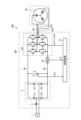
- FIG. 1 is a diagram showing a configuration example of a power conversion device 300 according to the first embodiment.
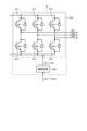
- FIG. 2 is a diagram showing a configuration example of an inverter 30 included in the power conversion device 300 according to the first embodiment.
- the power conversion device 300 is connected to an AC power source 1 and a compressor 50.
- the compressor 50 is an example of a load having a characteristic that the load torque varies periodically when driven.
- the compressor 50 has an electric motor 7.
- An example of the electric motor 7 is a three-phase permanent magnet synchronous motor.
- the power conversion device 300 converts a power supply voltage applied from the AC power source 1 into an AC voltage having a desired amplitude and phase and applies it to the electric motor 7.
- the power conversion device 300 includes a reactor 2, a converter 3, a capacitor 5, a voltage detection unit 8, a control device 10, an inverter 30, and a current detection unit 40.
- the power conversion device 300 and the electric motor 7 included in the compressor 50 constitute an electric motor drive device 400.
- the converter 3 has four diodes D1, D2, D3, and D4.
- the four diodes D1 to D4 are bridge-connected to form a rectifier circuit.
- the converter 3 rectifies the power supply voltage applied from the AC power supply 1 by the rectifier circuit made up of the four diodes D1 to D4.
- the converter 3 one end on the input side is connected to the AC power supply 1 via the reactor 2, and the other end on the input side is connected to the AC power supply 1.
- the output side is connected to the capacitor 5.
- the converter 3 may have a rectification function as well as a boost function for boosting the rectified voltage.
- a converter with a boost function may be configured with one or more transistor elements, or one or more switching elements in which a transistor element and a diode are connected in anti-parallel, in addition to or instead of a diode.
- the arrangement and connection of the transistor elements or switching elements in a converter with a boost function are publicly known, and will not be described here.
- Capacitor 5 is connected to the output terminal of converter 3 via DC buses 9a and 9b.
- DC bus 9a is the positive DC bus
- DC bus 9b is the negative DC bus.
- Capacitor 5 smoothes the rectified voltage applied from converter 3. Examples of capacitor 5 include an electrolytic capacitor and a film capacitor.
- the inverter 30 is connected to both ends of the capacitor 5 via the DC buses 9a and 9b.
- the inverter 30 converts the DC voltage smoothed by the capacitor 5 into an AC voltage for the compressor 50 and applies it to the motor 7 of the compressor 50.
- the voltage applied to the motor 7 is a three-phase AC voltage with variable frequency and voltage value.
- the inverter 30 includes an inverter main circuit 310 and a drive circuit 350.
- the inverter main circuit 310 includes switching elements 311 to 316. Rectifier elements 321 to 326 for reflux are connected in inverse parallel to each of the switching elements 311 to 316.
- the switching elements 311 to 316 may be made of a material other than silicon (Si), such as wide bandgap semiconductors as silicon carbide (SiC), gallium nitride (GaN), diamond, etc. By forming the switching elements 311 to 316 using wide bandgap semiconductors, it is possible to further reduce losses.
- Si silicon
- SiC silicon carbide
- GaN gallium nitride
- the voltage detection unit 8 detects the bus voltage Vdc by detecting the voltage across the capacitor 5.
- the bus voltage Vdc is the voltage between the DC buses 9a and 9b.
- the voltage detection unit 8 includes a voltage divider circuit that divides the voltage using resistors connected in series, for example.
- the voltage detection unit 8 converts the detected bus voltage Vdc into a voltage suitable for processing in the control device 10, for example a voltage of 5 V or less, using the voltage divider circuit, and outputs the voltage detection signal, which is an analog signal, to the control device 10.
- the voltage detection signal output from the voltage detection unit 8 to the control device 10 is converted from an analog signal to a digital signal by an AD (Analog to Digital) conversion unit (not shown) in the control device 10, and is used for internal processing in the control device 10.
- AD Analog to Digital
- the current detection unit 40 has a shunt resistor inserted in the DC bus 9b.
- the current detection unit 40 detects the capacitor output current i.d.c. using the shunt resistor.
- the capacitor output current i.d.c. is the input current to the inverter 30, i.e., the current output from the capacitor 5 to the inverter 30.
- the current detection unit 40 outputs the detected capacitor output current i.d.c. to the control device 10 as a current detection signal, which is an analog signal.
- the current detection signal output from the current detection unit 40 to the control device 10 is converted from an analog signal to a digital signal by an AD conversion unit (not shown) in the control device 10, and is used for internal processing in the control device 10.
- the control device 10 generates the aforementioned PWM signals Sm1 to Sm6 to control the operation of the inverter 30. Specifically, the control device 10 changes the angular frequency ⁇ e and voltage value of the inverter output voltage based on the PWM signals Sm1 to Sm6.
- the angular frequency ⁇ e of the inverter output voltage determines the rotational angular velocity in electrical angle of the motor 7.
- this rotational angular velocity will also be represented by the same symbol ⁇ e.
- the rotational angular velocity ⁇ m in mechanical angle of the motor 7 is equal to the rotational angular velocity ⁇ e in electrical angle of the motor 7 divided by the number of pole pairs P. Therefore, there is a relationship expressed by the following equation (1) between the rotational angular velocity ⁇ m in mechanical angle of the motor 7 and the angular frequency ⁇ e of the inverter output voltage.
- the rotational angular velocity will sometimes be referred to simply as "rotational speed” and the angular frequency will sometimes be referred to simply as "frequency.”
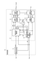
- FIG. 3 is a block diagram showing an example of the configuration of the control device 10 provided in the power conversion device 300 according to the first embodiment.
- the control device 10 includes an operation control unit 11 and an inverter control unit 12.
- the inverter control unit 12 includes a voltage command calculation unit 13, an electrical angle phase calculation unit 14, a space vector modulation unit 15, a PWM signal generation unit 16, a current restoration unit 17, a coordinate conversion unit 18, and an excitation current command control unit 19.
- the current restoration unit 17 restores the phase currents iu, iv, iw flowing through the motor 7 based on the capacitor output current idc detected by the current detection unit 40, and inputs them to the coordinate conversion unit 18.
- the current restoration unit 17 can restore the phase currents iu, iv, iw by sampling the detection value of the capacitor output current idc detected by the current detection unit 40 at a timing determined based on the PWM signals Sm1 to Sm6 generated by the PWM signal generation unit 16.
- a current detector may be provided on the output lines 331 to 333 to directly detect the phase currents iu, iv, iw and input them to the coordinate conversion unit 18. In this configuration, the current restoration unit 17 is not necessary.
- the coordinate conversion unit 18 converts the phase currents iu, iv, and iw restored by the current restoration unit 17 into the d-axis current id, which is the excitation current, and the q-axis current iq, which is the torque current, i.e., the current values of the d and q axes, using the electrical angle phase ⁇ e generated by the electrical angle phase calculation unit 14 described below.
- the excitation current command control unit 19 generates a d-axis current command id*, which is an excitation current command, based on the q-axis current iq acquired from the coordinate conversion unit 18, the command modulation factor M acquired from the operation control unit 11, and the d-axis voltage command Vd** and the q-axis voltage command Vq** calculated by the voltage command calculation unit 13 described later.
- the excitation current command control unit 19 obtains a current phase angle at which the output torque of the motor 7 is equal to or greater than a set value or is at its maximum value, and calculates the d-axis current command id* based on the obtained current phase angle.
- the excitation current command control unit 19 When calculating the d-axis current command id*, the excitation current command control unit 19 performs flux-weakening control and command modulation factor correction to determine the d-axis current command id*. The specific configuration and operation of the excitation current command control unit 19 will be described later.
- the excitation current command control unit 19 may calculate the d-axis current command id* using the motor current flowing through the motor 7 instead of the output torque of the motor 7. In this case, the d-axis current command id* is calculated based on the current phase angle at which the motor current flowing through the motor 7 is equal to or less than the set value or is at its minimum value.
- the voltage command calculation unit 13 generates a d-axis voltage command Vd**, a q-axis voltage command Vq**, a frequency estimate ⁇ est, a command modulation factor M*, and a voltage phase ⁇ v based on the frequency command ⁇ e* acquired from the operation control unit 11, the d-axis current id and the q-axis current iq acquired from the coordinate conversion unit 18, and the d-axis current command id* acquired from the excitation current command control unit 19.
- the command modulation factor M* and the voltage phase ⁇ v are used in the space vector modulation unit 15, the d-axis voltage command Vd** and the q-axis voltage command Vq** are used in the excitation current command control unit 19, and the frequency estimate ⁇ est is used inside the electrical angle phase calculation unit 14 and the voltage command calculation unit 13.
- the former is called the "first command modulation factor” and the latter is called the "second command modulation factor”.
- the electrical angle phase calculation unit 14 calculates the electrical angle phase ⁇ e by integrating the frequency estimate value ⁇ est obtained from the voltage command calculation unit 13.
- the space vector modulation unit 15 uses the command modulation factor M* and voltage phase ⁇ v obtained from the voltage command calculation unit 13, and the electrical angle phase ⁇ e obtained from the electrical angle phase calculation unit 14 to generate three-phase voltage commands Vu*, Vv*, and Vw*, which are output voltage commands in a three-phase coordinate system.
- the PWM signal generation unit 16 generates PWM signals Sm1 to Sm6 based on the three-phase voltage commands Vu*, Vv*, and Vw* obtained from the space vector modulation unit 15.
- Space vector modulation is a modulation method that combines six basic space vectors and two zero vectors to generate a voltage vector of any size at any position in a hexagon and in the vector space within the hexagon. For each PWM modulation period, the PWM signal generation unit 16 uses the switching pattern of two adjacent space vectors for a specified period and the zero vector for the remaining period to generate PWM signals Sm1 to Sm6 with controlled switching patterns and pulse on-times, and outputs them to the inverter 30.
- FIG 4 is a diagram showing the relationship between the command modulation rate and the actual modulation rate in a typical inverter.
- the region where the command modulation rate shown on the horizontal axis exceeds 1 is the overmodulation region.
- the command modulation rate is a value indicating the ratio of the voltage command amplitude in the voltage command given to the inverter 30 to the DC voltage value applied to the inverter 30.
- the actual modulation rate shown on the vertical axis is a value indicating the ratio of the inverter output voltage to that DC voltage value.
- the relationship between the command modulation rate and the actual modulation rate has nonlinear characteristics.
- FIG. 5 is a diagram used to explain the modulation factor correction method described in the Background section.
- the overmodulation region is a region in which the relationship between the voltage command and the inverter output voltage is nonlinear and not proportional. For this reason, in this overmodulation region, as shown in FIG. 5, control is performed to obtain the intended inverter output voltage by multiplying a nonlinear modulation factor correction coefficient according to the actual modulation factor value.
- the value of the modulation factor correction coefficient in the modulation factor correction method has a steep characteristic with respect to the actual modulation factor value. For this reason, as explained in the background section, if the modulation factor correction method and flux-weakening control are simply combined, the voltage command will become an excessive value due to the correction of the modulation factor, which may cause a problem that operation in the overmodulation region is likely to become unstable. Therefore, in this paper, we propose the following two methods to address this problem.
- First method A method of performing flux-weakening control using a voltage command after modulation factor correction.
- Second method A method of performing flux-weakening control using a voltage command before modulation factor correction.
- FIG. 6 is a block diagram showing an example of the configuration of the voltage command calculation unit 13 provided in the control device 10 of the power conversion device 300 according to the first embodiment.
- the voltage command calculation unit 13 includes adders 130, 132, and 133, a speed controller 131, a d-axis current controller 134, a q-axis current controller 135, a frequency estimation unit 136, a voltage command amplitude calculation unit 137, a modulation rate correction coefficient calculation unit 138, and a command modulation rate and voltage phase calculation unit 140.
- the speed controller 131 calculates and outputs the q-axis current command iq*, which is a torque current command, based on the frequency deviation del_ ⁇ .
- the q-axis current command iq* is the command value of the q-axis current iq at which the frequency deviation del_ ⁇ becomes zero, that is, the command value of the q-axis current iq for matching the frequency command ⁇ e* with the frequency estimate value ⁇ est.
- An example of the speed controller 131 is a Proportional-Integral (PI) controller, but is not limited to this example.
- the adder/subtractor 132 subtracts the d-axis current id from the d-axis current command id* and outputs the deviation between the d-axis current command id* and the d-axis current id.
- the d-axis current controller 134 performs PI control to converge the deviation between the d-axis current command id* and the d-axis current id to zero.
- the adder/subtracter 133 subtracts the q-axis current iq from the q-axis current command iq* and outputs the deviation between the q-axis current command iq* and the q-axis current iq.
- the q-axis current controller 135 performs PI control to converge the deviation between the q-axis current command iq* and the q-axis current iq to zero.
- the voltage command amplitude Vdq*_abs calculated by the voltage command amplitude calculation unit 137 is divided by a value obtained by multiplying the bus voltage Vdc by 1/ ⁇ 2 and input to the modulation rate correction coefficient calculation unit 138.
- the modulation rate correction coefficient calculation unit 138 calculates the modulation rate correction coefficient K using the voltage command amplitude Vdq*_abs.
- the modulation rate correction coefficient calculation unit 138 holds a table of characteristics as shown in FIG. 5.
- the modulation rate correction coefficient calculation unit 138 recognizes the input value as a command modulation rate, and when the input value is 1 or less, sets the value of the modulation rate correction coefficient K to be multiplied by the command modulation rate to "1.0", and when the voltage command amplitude Vdq*_abs exceeds 1, sets and outputs the corresponding value of the modulation rate correction coefficient K.
- the means for realizing the modulation rate correction coefficient calculation unit 138 does not have to be a table.
- the modulation rate correction coefficient calculation unit 138 may be configured to determine the value of the modulation rate correction coefficient K corresponding to the command modulation rate by calculation processing.
- the d-axis voltage command Vd** and q-axis voltage command Vq** calculated by the voltage command calculation unit 13 are output to the command modulation rate and voltage phase calculation unit 140 inside the voltage command calculation unit 13.
- the d-axis voltage command Vd** and q-axis voltage command Vq** calculated by the voltage command calculation unit 13 are output to the excitation current command control unit 19 shown in FIG. 3 outside the voltage command calculation unit 13.
- FIG. 7 is a block diagram showing an example configuration of a command modulation rate and voltage phase calculation unit 140 provided in a voltage command calculation unit 13 in a control device 10 of a power conversion device 300 according to embodiment 1.
- the command modulation rate and voltage phase calculation unit 140 includes a command modulation rate calculation unit 141 and a voltage phase calculation unit 144.
- the command modulation rate calculation unit 141 includes a voltage command amplitude calculation unit 142.
- the command modulation rate calculation unit 141 receives the d-axis voltage command Vd**, the q-axis voltage command Vq**, and the bus voltage Vdc.
- the voltage command amplitude calculation unit 142 uses the d-axis voltage command Vd** and the q-axis voltage command Vq** to calculate the voltage command amplitude Vdq**_abs shown in the following equation (4).
- the voltage command amplitude Vdq**_abs calculated by the voltage command amplitude calculation unit 142 is divided by the bus voltage Vdc multiplied by 1/ ⁇ 2, and output as the command modulation factor M*.
- the voltage phase calculation unit 144 also uses the d-axis voltage command Vd** and the q-axis voltage command Vq** to calculate the voltage phase ⁇ v shown in the following equation (5).
- command modulation factor M* and voltage phase ⁇ v calculated by the command modulation factor and voltage phase calculation unit 140 are used by the space vector modulation unit 15.
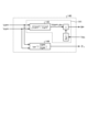
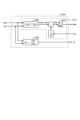
- FIG. 8 is a block diagram showing an example of the configuration of the excitation current command control unit 19 provided in the inverter control unit 12 in the control device 10 of the power conversion device 300 according to the first embodiment.
- the excitation current command control unit 19 includes a voltage command amplitude calculation unit 191, an adder/subtractor 192, an MTPA (Maximum Torque Per Ampere) control unit 193, an I (Integral) controller 194, and an id* comparison unit 195.
- the d-axis voltage command Vd** and the q-axis voltage command Vq** are input to the voltage command amplitude calculation unit 191.
- the voltage command amplitude calculation unit 191 uses the d-axis voltage command Vd** and the q-axis voltage command Vq** to calculate the voltage command amplitude Vdq**_abs shown in the above formula (4).
- the MTPA control unit 193 performs MTPA control on the q-axis current iq obtained from the coordinate conversion unit 18, and calculates one d-axis current command id* to be input to the id* comparison unit 195.
- the MTPA control is a control that adjusts the current phase of the current flowing through the electric motor 7 so as to maximize the torque generated by the electric motor 7.
- the MTPA control is well known, and since general MTPA control is used in this paper, a detailed explanation will be omitted here.
- the command modulation factor M is divided by 1/ ⁇ 2 times the bus voltage Vdc, and the divided value is input to an adder/subtractor 192 as a voltage limit value Vom*, which is a limit value for the d-axis and q-axis voltages.
- the voltage command amplitude Vdq**_abs calculated by the voltage command amplitude calculation unit 191 is input to the adder/subtractor 192.
- the adder/subtractor 192 calculates the deviation between the voltage limit value Vom* and the voltage command amplitude Vdq**_abs, and inputs the calculated deviation to the I controller 194 as the voltage saturation amount ⁇ V.
- the I controller 194 integrates the voltage saturation amount ⁇ V to calculate another d-axis current command id* to be input to the id* comparison unit 195.
- the id* comparison unit 195 selects the larger value on the negative side from the d-axis current command id* output from the MTPA control unit 193 and the d-axis current command id* output from the I controller 194, and outputs the selected value as the d-axis current command id* to the voltage command calculation unit 13.
- the integral gain Kfw of the flux-weakening control in the I controller 194 is set by the following equation (6).
- ⁇ fw is the cutoff angular frequency when the I controller 194 is viewed as a low-pass filter
- Ld is the d-axis inductance
- ⁇ e is the angular frequency of the inverter output voltage, as described above.
- the voltage saturation amount is controlled so that the average value of the actual modulation rate, which is a value indicating the ratio of the inverter output voltage to the DC voltage value, is kept constant at a certain value.
- the voltage command that is fed back to the voltage limit value is controlled with good tracking, and the I controller 194 operates stably without windup or the like.
- the gain of the integral control in general flux-weakening control is ⁇ fw/( ⁇ eLd), but in the excitation current command control unit 19 in embodiment 1, the voltage command after modulation factor correction is used to perform flux-weakening control, so the modulation factor correction coefficient K is required in the denominator of the integral gain Kfw, as in equation (6) above.
- the integral gain Kfw shown in equation (6) above it is possible to stabilize operation in the overmodulation region even when the modulation factor correction method and flux-weakening control are combined.
- the power conversion device includes a converter that rectifies the power supply voltage applied from the AC power supply, a capacitor connected to the output terminal of the converter, an inverter connected to both ends of the capacitor, and a control device that controls the operation of the inverter.
- the control device corrects the voltage command so that the inverter output voltage can be output linearly, and performs flux-weakening control when a voltage saturation amount calculated from the voltage limit value determined by the DC voltage value and the voltage command occurs.
- This flux-weakening control may be performed using the voltage command after the modulation rate correction, or may be performed using the voltage command before the modulation rate correction.
- the control device according to the first embodiment performs flux-weakening control using the voltage command after the modulation rate correction. That is, the power conversion device according to the first embodiment performs flux-weakening control using the voltage command after the modulation rate correction so that the inverter output voltage can be output linearly while stabilizing the operation in the overmodulation region.
- the control device calculates an excitation current command used in flux-weakening control based on a voltage saturation amount calculated from a voltage command and a voltage limit value determined by a DC voltage value.
- the voltage saturation amount is controlled so that the average value of the actual modulation factor, which is a value indicating the ratio of the inverter output voltage to the DC voltage value, becomes constant at a certain value, thereby stabilizing the operation of the control device.
- the gain of the flux-weakening control is an important parameter for stabilizing the operation of the control device.
- the control device is configured to determine the excitation current command for the flux-weakening control from the voltage command after modulation factor correction, as in embodiment 1, it is desirable to set the gain of the flux-weakening control including the modulation factor correction coefficient. Configuring the control device with this in mind can contribute to stabilizing the operation of the control device.
- FIG. 9 is a diagram showing an example of a hardware configuration realizing the control device 10 provided in the power conversion device 300 according to the first embodiment.
- the control device 10 is realized by a processor 201 and a memory 202.
- the processor 201 is a CPU (Central Processing Unit), central processing unit, processing unit, arithmetic unit, microprocessor, microcomputer, processor, DSP (Digital Signal Processor), or system LSI (Large Scale Integration).
- Examples of the memory 202 include non-volatile or volatile semiconductor memories such as RAM (Random Access Memory), ROM (Read Only Memory), flash memory, EPROM (Erasable Programmable Read Only Memory), and EEPROM (registered trademark) (Electrically Erasable Programmable Read-Only Memory).
- the memory 202 is not limited to these, and may be a magnetic disk, optical disk, compact disk, mini disk, or DVD (Digital Versatile Disc).
- Embodiment 2 a control device that uses the above-mentioned second technique, that is, a technique for performing flux-weakening control using a voltage command before modulation factor correction, will be described.
- FIG. 10 is a block diagram showing an example of the configuration of a control device 10A provided in a power conversion device 300 according to the second embodiment.
- the control device 10A includes an operation control unit 11 and an inverter control unit 12A.
- the inverter control unit 12A includes a voltage command calculation unit 13A, an electrical angle phase calculation unit 14, a space vector modulation unit 15, a PWM signal generation unit 16, a current restoration unit 17, a coordinate conversion unit 18, and an excitation current command control unit 19A.
- components having different functions from the control device 10 of the first embodiment shown in FIG. 3 are indicated with the subscript A.
- FIGS. 11, 12, and 13 The same applies to the drawings of FIGS. 11, 12, and 13.
- the second embodiment will be described with a focus on the functions of the components that are different from those of the first embodiment.
- the excitation current command control unit 19A generates a d-axis current command id*, which is an excitation current command, based on the q-axis current iq, the command modulation factor M obtained from the operation control unit 11, and the d-axis voltage command Vd* and q-axis voltage command Vq* calculated by the voltage command calculation unit 13A.
- the excitation current command control unit 19A finds a current phase angle at which the output torque of the motor 7 is equal to or greater than a set value or is at its maximum value, and calculates the d-axis current command id* based on the found current phase angle.
- the excitation current command control unit 19A When calculating the d-axis current command id*, the excitation current command control unit 19A performs flux-weakening control and command modulation factor correction to determine the d-axis current command id*. The specific configuration and operation of the excitation current command control unit 19A will be described later.
- the excitation current command control unit 19A may calculate the d-axis current command id* using the motor current flowing through the motor 7 instead of the output torque of the motor 7. In this case, the d-axis current command id* is calculated based on the current phase angle at which the motor current flowing through the motor 7 is equal to or less than the set value or is at its minimum value.
- the voltage command calculation unit 13A generates a d-axis voltage command Vd*, a q-axis voltage command Vq*, a frequency estimate ⁇ est, a command modulation factor M**, and a voltage phase ⁇ v based on the frequency command ⁇ e* obtained from the operation control unit 11, the d-axis current id and the q-axis current iq obtained from the coordinate conversion unit 18, and the d-axis current command id* obtained from the excitation current command control unit 19A.
- the command modulation factor M** and the voltage phase ⁇ v are used in the space vector modulation unit 15, the d-axis voltage command Vd* and the q-axis voltage command Vq* are used in the excitation current command control unit 19A, and the frequency estimate ⁇ est is used inside the electrical angle phase calculation unit 14 and the voltage command calculation unit 13A.
- FIG. 11 is a block diagram showing an example of the configuration of a voltage command calculation unit 13A provided in a control device 10A of a power conversion device 300 according to embodiment 2.
- the voltage command calculation unit 13A includes adders 130, 132, and 133, a speed controller 131, a d-axis current controller 134, a q-axis current controller 135, a frequency estimation unit 136, and a command modulation rate and voltage phase calculation unit 140A.
- the second embodiment employs a method of performing flux-weakening control using a voltage command before modulation rate correction, and therefore components such as the voltage command amplitude calculation unit 137 and the modulation rate correction coefficient calculation unit 138 are not necessary.
- the d-axis voltage command Vd* and q-axis voltage command Vq* calculated by the voltage command calculation unit 13A are output to the command modulation rate and voltage phase calculation unit 140A inside the voltage command calculation unit 13A. Also, the d-axis voltage command Vd* and q-axis voltage command Vq* calculated by the voltage command calculation unit 13A are output to the excitation current command control unit 19A shown in FIG. 10 outside the voltage command calculation unit 13A.
- FIG. 12 is a block diagram showing an example of the configuration of a command modulation rate and voltage phase calculation unit 140A provided in a voltage command calculation unit 13A in a control device 10A of a power conversion device 300 according to embodiment 2.
- the command modulation rate and voltage phase calculation unit 140A includes a command modulation rate calculation unit 141A and a voltage phase calculation unit 144A.
- the command modulation rate calculation unit 141A also includes a voltage command amplitude calculation unit 142A and a command modulation rate correction unit 146A.
- the command modulation rate calculation unit 141A receives the d-axis voltage command Vd*, the q-axis voltage command Vq*, and the bus voltage Vdc.
- the voltage command amplitude calculation unit 142A uses the d-axis voltage command Vd* and the q-axis voltage command Vq* to calculate the voltage command amplitude Vdq*_abs shown in the following equation (7).
- Vdq*_abs ⁇ (Vd* 2 +Vq* 2 ) ...(7)
- the voltage command amplitude Vdq*_abs calculated by the voltage command amplitude calculation unit 142A is divided by the bus voltage Vdc multiplied by 1/ ⁇ 2, and input to the command modulation factor correction unit 146A as the command modulation factor M*.
- the command modulation factor M* input to the command modulation factor correction unit 146A is calculated using the voltage command before modulation factor correction.
- the command modulation factor correction unit 146A has a table equivalent to that of the modulation factor correction coefficient calculation unit 138. If the value of the command modulation factor M* input is 1 or less, the command modulation factor correction unit 146A outputs the value of the command modulation factor M* as is, and if the value of the command modulation factor M* exceeds 1, it multiplies the command modulation factor M* by the corresponding modulation factor correction coefficient K and outputs the multiplied value as the command modulation factor M**.
- the voltage phase calculation unit 144A uses the d-axis voltage command Vd* and the q-axis voltage command Vq* to calculate the voltage phase ⁇ v shown in the following equation (8).
- the command modulation rate M** and voltage phase ⁇ v calculated by the command modulation rate and voltage phase calculation unit 140A are used by the space vector modulation unit 15.
- FIG. 13 is a block diagram showing an example of the configuration of an excitation current command control unit 19A provided in an inverter control unit 12A in a control device 10A of a power conversion device 300 according to embodiment 2.
- the excitation current command control unit 19A includes a voltage command amplitude calculation unit 191A, an adder/subtractor 192, an MTPA control unit 193, an I controller 194A, an id* comparison unit 195, and a command modulation factor correction unit 196.
- the d-axis voltage command Vd* and the q-axis voltage command Vq* are input to the voltage command amplitude calculation unit 191A.
- the voltage command amplitude calculation unit 191A uses the d-axis voltage command Vd* and the q-axis voltage command Vq* to calculate the voltage command amplitude Vdq*_abs shown in the above formula (7).
- the MTPA control unit 193 performs MTPA control on the q-axis current iq obtained from the coordinate conversion unit 18, and calculates a single d-axis current command id* to be input to the id* comparison unit 195.
- the command modulation factor correction unit 196 has a table equivalent to that of the command modulation factor correction unit 146A.
- the command modulation factor correction unit 196 When the value of the command modulation factor M input is 1 or less, the command modulation factor correction unit 196 outputs the value of the command modulation factor M as is, and when the value of the command modulation factor M exceeds 1, the command modulation factor correction unit 196 multiplies the command modulation factor M by the reciprocal 1/K of the corresponding modulation factor correction coefficient K and outputs the multiplied value.
- the command modulation factor M is multiplied by the reciprocal 1/K in order to align the comparison level with the voltage command amplitude Vdq*_abs output from the voltage command amplitude calculation unit 191A. In other words, since the voltage command amplitude Vdq*_abs is generated using the voltage command before the modulation factor correction, the command modulation factor M is multiplied by the reciprocal 1/K in relation to this process.
- the output of the command modulation rate correction unit 196 is divided by 1/ ⁇ 2 times the bus voltage Vdc, and the divided value is input to the adder/subtractor 192 as the voltage limit value Vom*, which is the limit value of the d-axis and q-axis voltages.
- the voltage command amplitude Vdq*_abs calculated by the voltage command amplitude calculation unit 191A is input to the adder/subtractor 192.
- the adder/subtractor 192 calculates the deviation between the voltage limit value Vom* and the voltage command amplitude Vdq*_abs, and inputs the calculated deviation to the I controller 194A as the voltage saturation amount ⁇ V'.
- the I controller 194A integrates the voltage saturation amount ⁇ V' to calculate another d-axis current command id* to be input to the id* comparison unit 195.
- the integral gain Kfw of the flux-weakening control in the I controller 194A is set by the following equation (9).
- ⁇ fw is the cutoff angular frequency when the I controller 194A is viewed as a low-pass filter
- Ld is the d-axis inductance
- ⁇ e is the angular frequency of the inverter output voltage, as described above.
- the voltage saturation amount is controlled so that the average value of the actual modulation rate, which is a value indicating the ratio of the inverter output voltage to the DC voltage value, is kept constant at a certain value.
- the voltage command that is fed back to the voltage limit value is controlled with good tracking, and the I controller 194A operates stably without windup or the like.
- the voltage command after modulation factor correction is used to perform flux-weakening control, so the modulation factor correction coefficient K was required in the denominator of the integral gain Kfw as in the above formula (6).
- the voltage command before modulation factor correction is used to perform flux-weakening control, so the modulation factor correction coefficient K is not required as in the above formula (9).
- an integral gain using the modulation factor correction coefficient K is used as in the excitation current command control unit 19 in the first embodiment, the operation becomes unstable. Therefore, by using the integral gain Kfw shown in the above formula (9), it is possible to stabilize operation in the overmodulation region even when the modulation factor correction method and flux-weakening control are combined.
- the power conversion device includes a converter that rectifies the power supply voltage applied from an AC power supply, a capacitor connected to the output terminal of the converter, an inverter connected across the capacitor, and a control device that controls the operation of the inverter.
- the control device corrects the voltage command so that the inverter output voltage can be output linearly, and performs flux-weakening control when a voltage saturation amount calculated from the voltage limit value determined by the DC voltage value and the voltage command occurs.
- the power conversion device performs flux-weakening control using the voltage command before modulation factor correction so that the inverter output voltage can be output linearly while stabilizing operation in the overmodulation region.
- the control device calculates an excitation current command used in the flux-weakening control based on the voltage saturation amount calculated from the voltage command and the voltage limit value determined by the DC voltage value and the modulation rate correction coefficient.
- the voltage saturation amount is controlled so that the average value of the actual modulation rate, which is a value indicating the ratio of the inverter output voltage to the DC voltage value, becomes constant at a certain value, thereby stabilizing the operation of the control device.
- the gain of the flux-weakening control is an important parameter for stabilizing the operation of the control device.
- the control device is configured to determine the excitation current command for the flux-weakening control from the voltage command before modulation factor correction, as in embodiment 2, it is desirable to set the gain of the flux-weakening control without including the modulation factor correction coefficient. Configuring the control device with this in mind can contribute to stabilizing the operation of the control device.
- Fig. 14 is a diagram showing a configuration example of a refrigeration cycle-applied device 900 according to embodiment 3.
- the refrigeration cycle-applied device 900 according to embodiment 3 includes the power conversion device 300 described in embodiment 1 or embodiment 2.
- the refrigeration cycle-applied device 900 according to embodiment 3 can be applied to products including a refrigeration cycle, such as air conditioners, refrigerators, freezers, and heat pump water heaters.
- a refrigeration cycle such as air conditioners, refrigerators, freezers, and heat pump water heaters.
- components having the same functions as those in embodiment 1 are denoted by the same reference numerals as those in embodiment 1.
- the refrigeration cycle application device 900 includes a compressor 50 incorporating the electric motor 7 in the first or second embodiment, a four-way valve 902, an indoor heat exchanger 906, an expansion valve 908, and an outdoor heat exchanger 910, which are attached via a refrigerant pipe 912.
- the refrigeration cycle device 900 can perform heating or cooling operation by switching the four-way valve 902.
- the compression mechanism 52 is driven by a variable speed controlled electric motor 7.
- the refrigerant is pressurized by the compression mechanism 52 and sent out, passes through the four-way valve 902, the indoor heat exchanger 906, the expansion valve 908, the outdoor heat exchanger 910, and the four-way valve 902, and returns to the compression mechanism 52.
- the refrigerant is pressurized by the compression mechanism 52 and sent out, passes through the four-way valve 902, the outdoor heat exchanger 910, the expansion valve 908, the indoor heat exchanger 906, and the four-way valve 902, and returns to the compression mechanism 52.
- the indoor heat exchanger 906 acts as a condenser to release heat, and the outdoor heat exchanger 910 acts as an evaporator to absorb heat.
- the outdoor heat exchanger 910 acts as a condenser to release heat, and the indoor heat exchanger 906 acts as an evaporator to absorb heat.
- the expansion valve 908 reduces the pressure of the refrigerant to expand it.
Landscapes
- Engineering & Computer Science (AREA)
- Power Engineering (AREA)
- Control Of Ac Motors In General (AREA)
Priority Applications (2)
| Application Number | Priority Date | Filing Date | Title |
|---|---|---|---|
| JP2025548061A JPWO2025069181A1 (https=) | 2023-09-26 | 2023-09-26 | |
| PCT/JP2023/034922 WO2025069181A1 (ja) | 2023-09-26 | 2023-09-26 | 電力変換装置、電動機駆動装置及び冷凍サイクル適用機器 |
Applications Claiming Priority (1)
| Application Number | Priority Date | Filing Date | Title |
|---|---|---|---|
| PCT/JP2023/034922 WO2025069181A1 (ja) | 2023-09-26 | 2023-09-26 | 電力変換装置、電動機駆動装置及び冷凍サイクル適用機器 |
Publications (1)
| Publication Number | Publication Date |
|---|---|
| WO2025069181A1 true WO2025069181A1 (ja) | 2025-04-03 |
Family
ID=95202576
Family Applications (1)
| Application Number | Title | Priority Date | Filing Date |
|---|---|---|---|
| PCT/JP2023/034922 Pending WO2025069181A1 (ja) | 2023-09-26 | 2023-09-26 | 電力変換装置、電動機駆動装置及び冷凍サイクル適用機器 |
Country Status (2)
| Country | Link |
|---|---|
| JP (1) | JPWO2025069181A1 (https=) |
| WO (1) | WO2025069181A1 (https=) |
Citations (5)
| Publication number | Priority date | Publication date | Assignee | Title |
|---|---|---|---|---|
| JPH1127996A (ja) * | 1997-06-30 | 1999-01-29 | Yaskawa Electric Corp | Acモータ用電流ベクトル制御方法およびacモータ駆動装置 |
| JP2010068662A (ja) * | 2008-09-11 | 2010-03-25 | Mitsubishi Electric Corp | 電動機の駆動装置並びに冷凍空調装置 |
| JP2017046430A (ja) * | 2015-08-26 | 2017-03-02 | ジョンソンコントロールズ ヒタチ エア コンディショニング テクノロジー(ホンコン)リミテッド | モータ制御装置、流体機械、空気調和機およびプログラム |
| JP2019103267A (ja) * | 2017-12-04 | 2019-06-24 | 日立オートモティブシステムズ株式会社 | モータ駆動システム |
| JP6929434B2 (ja) * | 2018-02-26 | 2021-09-01 | 三菱電機株式会社 | 電動機駆動装置及び冷凍サイクル適用機器 |
-
2023
- 2023-09-26 WO PCT/JP2023/034922 patent/WO2025069181A1/ja active Pending
- 2023-09-26 JP JP2025548061A patent/JPWO2025069181A1/ja active Pending
Patent Citations (5)
| Publication number | Priority date | Publication date | Assignee | Title |
|---|---|---|---|---|
| JPH1127996A (ja) * | 1997-06-30 | 1999-01-29 | Yaskawa Electric Corp | Acモータ用電流ベクトル制御方法およびacモータ駆動装置 |
| JP2010068662A (ja) * | 2008-09-11 | 2010-03-25 | Mitsubishi Electric Corp | 電動機の駆動装置並びに冷凍空調装置 |
| JP2017046430A (ja) * | 2015-08-26 | 2017-03-02 | ジョンソンコントロールズ ヒタチ エア コンディショニング テクノロジー(ホンコン)リミテッド | モータ制御装置、流体機械、空気調和機およびプログラム |
| JP2019103267A (ja) * | 2017-12-04 | 2019-06-24 | 日立オートモティブシステムズ株式会社 | モータ駆動システム |
| JP6929434B2 (ja) * | 2018-02-26 | 2021-09-01 | 三菱電機株式会社 | 電動機駆動装置及び冷凍サイクル適用機器 |
Also Published As
| Publication number | Publication date |
|---|---|
| JPWO2025069181A1 (https=) | 2025-04-03 |
Similar Documents
| Publication | Publication Date | Title |
|---|---|---|
| JP3644391B2 (ja) | インバータ装置、圧縮機制御装置、冷凍・空調装置の制御装置、モータの制御方法、圧縮機、冷凍・空調装置 | |
| US10270380B2 (en) | Power converting apparatus and heat pump device | |
| CN116802982A (zh) | 电力转换装置 | |
| JP7566175B2 (ja) | 電力変換装置、電動機駆動装置及び冷凍サイクル適用機器 | |
| JP6982532B2 (ja) | 冷凍サイクル装置 | |
| WO2025069183A1 (ja) | 電力変換装置、電動機駆動装置及び冷凍サイクル適用機器 | |
| JP7166468B2 (ja) | 電動機駆動装置および冷凍サイクル適用機器 | |
| US20260078914A1 (en) | Motor drive device, air-sending device, air-conditioning apparatus, and motor driving method | |
| JP7566174B2 (ja) | 電力変換装置、電動機駆動装置及び冷凍サイクル適用機器 | |
| WO2025069181A1 (ja) | 電力変換装置、電動機駆動装置及び冷凍サイクル適用機器 | |
| JP7542751B2 (ja) | 電力変換装置、電動機駆動装置及び冷凍サイクル適用機器 | |
| US20240396486A1 (en) | Power conversion apparatus, motor drive apparatus, and refrigeration cycle application apparatus | |
| JP2020205708A (ja) | オープン巻線モータ駆動装置及び冷凍サイクル装置 | |
| JP6490540B2 (ja) | 回転位置検出装置,空気調和機及び回転位置検出方法 | |
| WO2020095377A1 (ja) | 負荷駆動装置、冷凍サイクル装置及び空気調和機 | |
| WO2023157045A1 (ja) | 電力変換装置および空気調和機 | |
| JP7361948B2 (ja) | 電動機駆動装置、冷凍サイクル装置、及び空気調和機 | |
| WO2025069182A1 (ja) | 電力変換装置、電動機駆動装置及び冷凍サイクル適用機器 | |
| CN118696497A (zh) | 马达驱动装置以及制冷循环装置 | |
| JP7799851B2 (ja) | 電力変換装置、モータ駆動装置および冷凍サイクル適用機器 | |
| WO2024075163A1 (ja) | 電力変換装置、モータ駆動装置および冷凍サイクル適用機器 | |
| JP7515740B2 (ja) | 電力変換装置、電動機駆動装置及び冷凍サイクル適用機器 | |
| JP7515739B2 (ja) | 電力変換装置、電動機駆動装置及び冷凍サイクル適用機器 | |
| US20260088743A1 (en) | Power converting apparatus, motor drive device, and refrigeration cycle-incorporating device | |
| WO2025109762A1 (ja) | 電力変換装置、モータ駆動装置および冷凍サイクル適用機器 |
Legal Events
| Date | Code | Title | Description |
|---|---|---|---|
| 121 | Ep: the epo has been informed by wipo that ep was designated in this application |
Ref document number: 23954158 Country of ref document: EP Kind code of ref document: A1 |
|
| ENP | Entry into the national phase |
Ref document number: 2025548061 Country of ref document: JP Kind code of ref document: A |
|
| WWE | Wipo information: entry into national phase |
Ref document number: 2025548061 Country of ref document: JP |