WO2025057268A1 - 半導体装置及び半導体装置の製造方法 - Google Patents
半導体装置及び半導体装置の製造方法 Download PDFInfo
- Publication number
- WO2025057268A1 WO2025057268A1 PCT/JP2023/033050 JP2023033050W WO2025057268A1 WO 2025057268 A1 WO2025057268 A1 WO 2025057268A1 JP 2023033050 W JP2023033050 W JP 2023033050W WO 2025057268 A1 WO2025057268 A1 WO 2025057268A1
- Authority
- WO
- WIPO (PCT)
- Prior art keywords
- external terminal
- semiconductor element
- terminal
- semiconductor device
- main
- Prior art date
- Legal status (The legal status is an assumption and is not a legal conclusion. Google has not performed a legal analysis and makes no representation as to the accuracy of the status listed.)
- Pending
Links
Images






Classifications
-
- H—ELECTRICITY
- H10—SEMICONDUCTOR DEVICES; ELECTRIC SOLID-STATE DEVICES NOT OTHERWISE PROVIDED FOR
- H10W—GENERIC PACKAGES, INTERCONNECTIONS, CONNECTORS OR OTHER CONSTRUCTIONAL DETAILS OF DEVICES COVERED BY CLASS H10
- H10W72/00—Interconnections or connectors in packages
-
- H—ELECTRICITY
- H10—SEMICONDUCTOR DEVICES; ELECTRIC SOLID-STATE DEVICES NOT OTHERWISE PROVIDED FOR
- H10W—GENERIC PACKAGES, INTERCONNECTIONS, CONNECTORS OR OTHER CONSTRUCTIONAL DETAILS OF DEVICES COVERED BY CLASS H10
- H10W72/00—Interconnections or connectors in packages
- H10W72/071—Connecting or disconnecting
-
- H—ELECTRICITY
- H10—SEMICONDUCTOR DEVICES; ELECTRIC SOLID-STATE DEVICES NOT OTHERWISE PROVIDED FOR
- H10W—GENERIC PACKAGES, INTERCONNECTIONS, CONNECTORS OR OTHER CONSTRUCTIONAL DETAILS OF DEVICES COVERED BY CLASS H10
- H10W90/00—Package configurations
Definitions
- This disclosure relates to a semiconductor device.
- Patent document 1 describes technology related to semiconductor devices.
- the present disclosure has been made in consideration of the above points, and aims to provide technology that can facilitate the assembly of semiconductor devices.
- One aspect of the semiconductor device includes a sealing material, a first semiconductor element, a first external terminal, a second external terminal, and a first insulating member.
- the first semiconductor element has a first surface and is covered with the sealing material.
- the first external terminal is bonded to the first surface.
- the second external terminal is located away from the first external terminal and is bonded to the first surface.
- the first insulating member connects the first external terminal and the second external terminal inside the sealing material.
- Another aspect of the method for manufacturing a semiconductor device is the method for manufacturing the above-mentioned semiconductor device, which includes the steps of preparing a member having a first external terminal, a second external terminal, and a first insulating member connecting the first external terminal and the second external terminal, and joining the first external terminal and the second external terminal of the member together to the first semiconductor element.
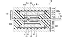
- FIG. 1 is a schematic diagram showing an example of a cross-sectional structure of a semiconductor device
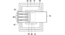
- FIG. 1 is a schematic plan view showing an example of a portion of a semiconductor device.
- FIG. 2 is a schematic perspective view showing an example of an integrated member.
- 1A to 1C are schematic diagrams illustrating an example of a method for manufacturing a semiconductor device.
- 1 is a schematic diagram showing an example of a cross-sectional structure of a semiconductor device; 1 is a schematic diagram showing an example of a cross-sectional structure of a semiconductor device; 1 is a schematic diagram showing an example of a cross-sectional structure of a semiconductor device; 1 is a schematic diagram showing an example of a cross-sectional structure of a semiconductor device; 1 is a schematic diagram showing an example of a cross-sectional structure of a semiconductor device; 1 is a schematic diagram showing an example of a cross-sectional structure of a semiconductor device; FIG. 1 is a schematic plan view showing an example of a portion of a semiconductor device.
- FIG. 1 is a schematic diagram showing an example of a cross-sectional structure of a semiconductor device; 1 is a schematic perspective view showing an example of a semiconductor device; FIG. 1 is a schematic plan view showing an example of a portion of a semiconductor device. FIG. 1 is a schematic plan view showing an example of a portion of a semiconductor device.
- Fig. 1 is a schematic diagram showing an example of a cross-sectional structure of a semiconductor device 1A according to embodiment 1.
- the semiconductor device 1A includes, for example, a base plate 10, an insulating substrate 20, a conductive pattern 30, a semiconductor element 40, external terminals 60 and 70, an insulating member 80, bonding materials 90, 91, and 92, and a sealing material 100.
- Fig. 2 is a schematic diagram showing an example of the semiconductor device 1A from which the sealing material 100 has been removed, as viewed from the top of Fig. 1.
- an insulating substrate 20 is provided on a base plate 10.
- a conductive pattern 30 is provided on the insulating substrate 20.
- a semiconductor element 40 is bonded to the conductive pattern 30 with a conductive bonding material 90.
- the bonding material 90 is located between the semiconductor element 40 and the conductive pattern 30.
- the conductive pattern 30 is electrically connected to the semiconductor element 40.
- the semiconductor device 1A includes, for example, a plurality of external terminals 60.
- Each external terminal 60 is bonded to the semiconductor element 40 with a conductive bonding material 91.
- the bonding material 91 is located between each external terminal 60 and the semiconductor element 40.
- the external terminal 70 is bonded to the semiconductor element 40 with a conductive bonding material 92.
- the bonding material 92 is located between the external terminal 70 and the semiconductor element 40.
- the external terminals 60 and 70 are electrically connected to the semiconductor element 40.
- FIG. 3 is a schematic diagram showing an example of a plurality of external terminals 60, an external terminal 70, and an insulating member 80.
- the plurality of external terminals 60 and the external terminal 70 are connected by an insulating member 80.
- the plurality of external terminals 60, the external terminal 70, and the insulating member 80 are integrated together to form an integrated member 50.
- the sealing material 100 is provided on the base plate 10 so as to cover the insulating substrate 20, the conductive pattern 30, the semiconductor element 40, the integrated member 50, and the bonding materials 90, 91, and 92. A portion of each external terminal 60 and a portion of the external terminal 70 are taken out to the outside of the sealing material 100. In other words, a portion of each external terminal 60 and a portion of the external terminal 70 are located outside the sealing material 100. Each of the external terminals 60 and 70 is also called, for example, a lead terminal.
- the sealing material 100 may be made of resin.
- the resin constituting the sealing material 100 may be silicone resin or epoxy resin.
- semiconductor device 1A each component of semiconductor device 1A will be described in detail.
- the upper, lower, left, right, rear, and front sides of FIG. 1 will be referred to as the upper, lower, left, right, rear, and front sides of semiconductor device 1A, respectively.
- the direction perpendicular to the up-down direction of semiconductor device 1A will be referred to as the horizontal direction.
- the horizontal direction of semiconductor device 1A includes the left-right and front-to-back directions of semiconductor device 1A.
- the definition of the upper side and the like also applies to semiconductor devices 1B, 1C, 1D, and 1E shown in FIGS. 8, 9, 10, and 12 described below.
- the semiconductor element 40 is, for example, a plate-shaped semiconductor chip diced from a semiconductor wafer.
- the semiconductor chip is also called, for example, a wafer chip or a die.
- the semiconductor element 40 may be formed of, for example, a semiconductor such as Si, or may be formed of a so-called wide band gap semiconductor such as SiC, GaN, Ga 2 O 3 , or diamond.
- the semiconductor element 40 is, for example, a power semiconductor element.
- the semiconductor element 40 may have a switching element such as an IGBT (Insulated Gate Bipolar Transistor) or a MOSFET (Metal Oxide Semiconductor Field Effect Transistor).
- the semiconductor element 40 may also have a switching element and a freewheel diode.
- the main electrode 42 is formed, for example, over the entire lower surface of the semiconductor element 40.
- the multiple signal electrodes 45 are arranged, for example, in a row along the front-to-rear direction at intervals.
- the main electrode 41 is arranged, for example, so as to face the multiple signal electrodes 45 in the left-to-right direction.
- the main electrode 41 is positioned away from each of the signal electrodes 45. Note that the arrangement of the signal electrodes 45, main electrodes 41, and main electrodes 42 is not limited to this example.
- the multiple external terminals 60 are respectively bonded to the multiple signal electrodes 45 on the upper surface of the semiconductor element 40 by bonding material 91.
- the multiple external terminals 60 are electrically connected to the multiple signal electrodes 45, respectively.
- the external terminals 60 can also be considered as signal terminals to which signals are input from outside the semiconductor device 1A or from inside the semiconductor device 1A, for example.
- the external terminals 60 may be referred to as signal terminals 60.
- the signal terminals 60 can also be considered as terminals that transmit signals.
- the external terminal 70 is joined to the main electrode 41 on the upper surface of the semiconductor element 40 by a joining material 92.
- the external terminal 70 is electrically connected to the main electrode 41.
- the external terminal 70 can also be referred to as, for example, a main terminal through which a main current flows.
- the external terminal 70 may be referred to as the main terminal 70.
- the insulating substrate 20 is made of an insulating material such as ceramic.
- the conductive pattern 30 is formed on the upper surface of the insulating substrate 20.
- the conductive pattern 30 is a metal layer made of, for example, copper or aluminum.
- the conductive pattern 30 is sometimes called a circuit pattern or a wiring pattern.
- the insulating substrate 20 and the conductive pattern 30 can be said to constitute, for example, a wiring substrate.
- the main electrode 42 on the lower surface of the semiconductor element 40 is joined to the conductive pattern 30 with a bonding material 90.
- the main electrode 42 is electrically connected to the conductive pattern 30.
- the insulating member 80 that connects the signal terminal 60 and the main terminal 70 is made of an insulating material.
- the material of the insulating member 80 may be, for example, ceramic or resin.
- the resin used as the material of the insulating member 80 may be, for example, phenol resin or epoxy resin.
- the semiconductor device 1A may also include an external terminal (also called a lead terminal) that is joined to the conductive pattern 30 with a conductive bonding material.
- the external terminal is electrically connected to the main electrode 42 (e.g., an emitter electrode) of the semiconductor element 40.
- the external terminals 60 and 70 are connected to each other by the insulating member 80, so that the external terminals 60 and 70 can be joined together to the semiconductor element 40. This makes it easier to assemble the semiconductor device 1A.
- FIG. 4 is a schematic diagram showing an example of a manufacturing method of the semiconductor device 1A.
- the insulating substrate 20 on which the conductive pattern 30 is formed is bonded to the base plate 10
- the semiconductor element 40 is bonded to the conductive pattern 30, and bonding materials 91 and 92 are provided on the upper surface of the semiconductor element 40.
- an integrated member 50 having a signal terminal 60, a main terminal 70, and an insulating member 80 connecting the signal terminal 60 and the main terminal 70 is prepared.
- the lower surface of the base plate 10 is heated by a heater block 900 to melt the bonding materials 91 and 92 provided on the upper surface of the semiconductor element 40.
- the signal terminal 60 and the main terminal 70 of the integrated member 50 are pressed against the bonding materials 91 and 92 in the melted state, and the signal terminal 60 and the main terminal 70 are bonded together to the upper surface of the semiconductor element 40. As a result, the structure shown in FIG. 2 is obtained. After that, a sealing material 100 is formed, and the semiconductor device 1A is completed.
- the heat from the heater block 900 is transferred to the signal terminal 60 through the base plate 10, insulating substrate 20, conductive pattern 30, semiconductor element 40, and bonding material 91 in this order.
- the heat from the heater block 900 is transferred to the main terminal 70 through the base plate 10, insulating substrate 20, conductive pattern 30, semiconductor element 40, and bonding material 92 in this order. Therefore, the heat input path to the signal terminal 60 and the heat input path to the main terminal 70 are the same. This allows the signal terminal 60 and the main terminal 70 to be heated in the same way, making it easier to join the signal terminal 60 and the main terminal 70 together to the top surface of the semiconductor element 40.
- the melting temperatures of the bonding materials 91 and 92 are approximately the same, it becomes easier to bond the signal terminals 60 and the main terminals 70 together to the semiconductor element 40.
- the melting temperatures of the bonding materials 91 and 92 will be approximately the same.
- the insulating member 80 is made of a material, such as ceramic, that has a sufficiently higher heat resistance than the material of the external terminals, the insulating member 80 does not become a rate limiter for the temperature rise when the signal terminals 60 and main terminals 70 are joined to the semiconductor element 40, and the signal terminals 60 and main terminals 70 can be appropriately heated to the required temperature. This makes it easier to join the signal terminals 60 and main terminals 70 to the semiconductor element 40 all at once.
- the insulating member 80 may have a portion that spans the signal terminal 60 and the main terminal 70. In this case, as shown in FIG. 5, the insulating member 80 may be directly joined to the upper surface of the main terminal 70 and the upper surface of the horizontal portion of the signal terminal 60 by casting or the like. Also, as shown in FIG. 6, the insulating member 80 may be joined to the upper surface of the main terminal 70 with a joining material 94, and to the upper surface of the horizontal portion of the signal terminal 60 with a joining material 93.
- the material of the joining materials 93 and 94 may be brazing material.
- the material of the joining material 93 and the material of the joining material 94 may be the same type as each other, or may be different types from each other.
- the insulating member 80 may have a portion that fills the gap between the signal terminal 60 and the main terminal 70, and a portion that spans the signal terminal 60 and the main terminal 70.
- Embodiment 2. 8 is a schematic diagram showing an example of a cross-sectional structure of a semiconductor device 1B according to embodiment 2.
- the semiconductor device 1B is configured by further providing plating layers 110 and 120 in the semiconductor device 1A according to embodiment 1 described above.
- a plating layer 110 having higher wettability with the bonding material 91 than the signal terminal 60 is provided in the area where the signal electrode 45 of the semiconductor element 40 is bonded.
- the plating layer 110 is plated in the area of the lower surface of the horizontal part of the signal terminal 60 where the signal electrode 45 is bonded.
- the bonding material 91 is located between the plating layer 110 and the signal electrode 45. It can also be said that the plating layer 110 and the signal electrode 45 are bonded with the bonding material 91.
- the plating layer 110 may be made of nickel, silver, or gold.
- the plating method of the plating layer 110 may be electrolytic plating or electroless plating.
- a plating layer 120 having higher wettability with the bonding material 92 than the main terminal 70 is provided in the region where the main electrode 41 of the semiconductor element 40 is bonded.
- the plating layer 120 is plated in the region of the lower surface of the main terminal 70 where the main electrode 41 is bonded.
- the bonding material 92 is located between the plating layer 120 and the main electrode 41. It can also be said that the plating layer 120 and the main electrode 41 are bonded with the bonding material 92.
- the plating layer 120 may be made of nickel, silver, or gold.
- the plating method of the plating layer 120 may be electrolytic plating or electroless plating.
- the material of the plating layer 120 may be the same type as the material of the plating layer 110, or may be a different type.
- the plating layer 110 which has a higher wettability with the bonding material 91 than the signal terminal 60, is provided in the area of the signal terminal 60 where the semiconductor element 40 is bonded, making it easier to bond the signal terminal 60 to the semiconductor element 40 with the bonding material 91.
- the plating layer 110 can define the area where the bonding material 91 wets and spreads, making it less likely that a volume shortage of the bonding material 91 will occur, making it easier to bond the signal terminal 60 to the semiconductor element 40.
- a plating layer 120 that has higher wettability with the bonding material 92 than the main terminal 70 is provided in the area of the main terminal 70 where the semiconductor element 40 is bonded, making it easier to bond the main terminal 70 to the semiconductor element 40 with the bonding material 92.
- the multiple signal terminals 60 may not be provided with the plating layer 110.
- the main terminal 70 may not be provided with the plating layer 120.
- Embodiment 3. 9 is a schematic diagram showing an example of a cross-sectional structure of a semiconductor device 1C according to the embodiment 3.
- the semiconductor device 1C is configured such that an integral member 50C is provided instead of the integral member 50 in the semiconductor device 1B according to the above-described embodiment 2.
- the integrated member 50C is the above-mentioned integrated member 50, in which signal terminals 60C are provided in place of each of the signal terminals 60.
- the signal terminals 60C include a first portion 61 having a relatively low strength and a second portion 62 having a relatively high strength.
- the first portion 61 constitutes, for example, a horizontal portion extending horizontally, specifically in the left-right direction, and the second portion 62 constitutes, for example, an upper-lower portion extending in the up-down direction.
- the first portion 61 is partially located outside the sealing material 100.
- the entire area of the second portion 62 is located outside the sealing material 100.
- One longitudinal end of the first portion 61 is joined to the signal electrode 45 of the semiconductor element 40 by a bonding material 91.
- a plating layer 110 is provided in the area where the signal electrode 45 is joined.
- the first portion 61 extends to the left from the semiconductor element 40 to the outside of the sealing material 100.
- the other longitudinal end of the first portion 61 is located outside the sealing material 100.
- the other longitudinal end of the first portion 61 is joined to the lower end of the second portion 62 located outside the sealing material 100 by a conductive bonding material 63.
- the material of the bonding material 63 may be solder or brazing material.
- the second portion 62 has a higher strength (e.g., tensile strength) than the first portion 61.
- tensile strength e.g., tensile strength
- the material of the first portion 61 is pure aluminum
- the material of the second portion 62 may be pure copper, a copper alloy, or an aluminum alloy.
- the material of the first portion 61 is an aluminum alloy
- the material of the second portion 62 may be a copper alloy.
- the second portion 62 also has a higher strength than the main terminal 70.
- the material of the main terminal 70 is pure aluminum
- the material of the second portion 62 may be pure copper, a copper alloy, or an aluminum alloy.
- the material of the main terminal 70 is an aluminum alloy
- the material of the second portion 62 may be a copper alloy. If the second portion 62 has a higher strength than the main terminal 70, it can be said that the signal terminal 60C has a portion that is stronger than the main terminal 70.
- a plating layer 64 having higher wettability of the bonding material 63 than the first portion 61 may be provided in the region of the first portion 61 where the second portion 62 is bonded.
- the plating layer 64 may be made of nickel, silver, or gold.
- the plating method of the plating layer 64 may be electrolytic plating or electroless plating.
- the material of the plating layer 64 may be the same type as the material of the plating layer 110 or may be a different type.
- the material of the plating layer 64 may be the same type as the material of the plating layer 120 or may be a different type.
- the signal terminal 60C can be said to have an internal portion 160 located inside the sealing material 100, and an external portion 161 located outside the sealing material 100.
- the internal portion 160 is composed of the portion of the first portion 61 located inside the sealing material 100.
- the external portion 161 is composed of the portion of the first portion 61 located outside the sealing material 100, the second portion 62, the bonding material 63, and the plating layer 64.
- the external portion 161 has a portion that is stronger than at least a portion of the internal portion 160.
- the external portion 161 also has a portion that is stronger than at least a portion of the main terminal 70.
- the signal terminal 60C has a portion that is stronger than at least a portion of the main terminal 70.
- the second portion 62 included in the external portion 161 has a strength greater than that of the internal portion 160 formed from a portion of the first portion 61, and greater than that of the main terminal 70.
- the external portion 161 has a portion that is stronger than the entire area of the internal portion 160 and the entire area of the main terminal 70.
- the end located outside the sealing material 100 is called the outer end.
- the outer portion 161 a specific part including the outer end of the signal terminal 60C has a strength higher than that of the inner portion 160 and the main terminal 70.
- the external portion 161 may have a portion that is stronger than a part of the internal portion 160, rather than the entire area of the internal portion 160.
- the second portion 62 may extend from the outside to the inside of the sealing material 100, and the second portion 62 and the first portion 61 may be joined with a joining material 63 inside the sealing material 100.
- the external portion 161 may have a portion that is stronger than a portion of the main terminal 70, rather than the entire area of the main terminal 70.
- the main terminal 70 may have a first portion made of the same type of material as the first portion 61, and a second portion made of the same type of material as the second portion 62.
- the signal terminal 60C has a portion that is stronger than a portion of the main terminal 70.
- the main terminal 70 of the integrated member 50C may have an external portion located outside the sealing material 100 that is stronger than at least a portion of the internal portion located inside the sealing material 100.
- the signal terminal 60C when the signal terminal 60C has a portion with a relatively high strength, the signal terminal 60C is less likely to undergo plastic deformation when it is joined to the semiconductor element 40 by the joining material 91. This makes it easier to join the signal terminal 60C to the semiconductor element 40. In addition, the reliability of the semiconductor device 1C is improved.
- the main terminal 70 has a portion with relatively high strength, the main terminal 70 is less likely to undergo plastic deformation when it is joined to the semiconductor element 40 by the joining material 92. This makes it easier to join the main terminal 70 to the semiconductor element 40. This also improves the reliability of the semiconductor device 1C.
- the external portion 161 of the signal terminal 60C has a portion with relatively high strength, the external portion 161 is less likely to undergo plastic deformation when, for example, a board such as a control board is inserted into the external portion 161.
- the external portion of the main terminal 70 has a relatively high strength portion, the external portion will be less likely to undergo plastic deformation, for example, when inserting a board into the external portion.
- the semiconductor device 1B according to the second embodiment has the integral member 50C instead of the integral member 50, but the semiconductor device 1A according to the first embodiment may have the integral member 50C instead of the integral member 50.
- the entire area of at least one of the multiple signal terminals 60 provided in the semiconductor devices 1A and 1B may be made of a material with relatively high strength, such as pure copper or a copper alloy.
- the entire area of the main terminal 70 may be made of a material with relatively high strength, such as pure copper or a copper alloy.
- Embodiment 4. 10 is a schematic diagram showing an example of a cross-sectional structure of a semiconductor device 1D according to a fourth embodiment.
- the semiconductor device 1D is obtained by adding a configuration 200a, which is the same as the configuration 200 consisting of a base plate 10, an insulating substrate 20, a conductive pattern 30, a semiconductor element 40, and bonding materials 90, 91, and 92, to the semiconductor device 1A.
- the base plate 10, the insulating substrate 20, the conductive pattern 30, the semiconductor element 40, and the bonding materials 90, 91, and 92 constituting the additional configuration 200a will be referred to as the base plate 10a, the insulating substrate 20a, the conductive pattern 30a, the semiconductor element 40a, and the bonding materials 90a, 91a, and 92a, respectively.
- the main electrode 41, the main electrode 42, and the signal electrode 45 provided in the semiconductor element 40a will be referred to as the main electrode 41a, the main electrode 42a, and the signal electrode 45a, respectively.
- the components 200 and 200a are arranged vertically with a portion of the integrated member 50 sandwiched between them.
- the component 200 is located on the lower side, and the component 200a is located on the upper side.
- the components 200a and 200 are arranged symmetrically vertically.
- the semiconductor element 40a is joined to the integrated member 50 on the side opposite the semiconductor element 40.
- the multiple signal electrodes 45a of the semiconductor element 40a are joined to the upper surfaces of the horizontal portions of the multiple signal terminals 60 with a bonding material 91a.
- the signal electrodes 45a of the semiconductor element 40a and the signal electrodes 45 of the semiconductor element 40 are electrically connected to each other.
- the main electrode 41a of the semiconductor element 40a is joined to the upper surface of the main terminal 70 with a bonding material 92a.
- the main electrode 41a of the semiconductor element 40a and the main electrode 41 of the semiconductor element 40 are electrically connected to each other.
- the semiconductor element 40a is joined to the signal terminals 60 and the main terminals 70 on the side opposite the semiconductor element 40.
- the sealing material 100 is located between the base plate 10 and the base plate 10a.
- the insulating substrate 20a, the conductive pattern 30a, the semiconductor element 40a, and the bonding materials 90a, 91a, and 92a of the configuration 200a are covered with the sealing material 100.
- one main electrode 41 (e.g., collector electrode) of the switching element of the semiconductor element 40 is electrically connected to one main electrode 41a (e.g., collector electrode) of the switching element of the semiconductor element 40a.
- the signal electrode 45 serving as a control electrode of the switching element of the semiconductor element 40 is electrically connected to the signal electrode 45a serving as a control electrode of the switching element of the semiconductor element 40a.
- FIG. 11 is a schematic diagram showing an example of the state of the integral member 50 and the configuration 200a shown in FIG. 10 as viewed from below.
- the base plate 10, the insulating substrate 20, the conductive pattern 30, and the semiconductor element 40 are arranged in the same manner in the configurations 200 and 200a.
- the positional relationship between the base plate 10, the insulating substrate 20, the conductive pattern 30, and the semiconductor element 40 in the configuration 200 is the same as the positional relationship between the base plate 10a, the insulating substrate 20a, the conductive pattern 30a, and the semiconductor element 40a in the configuration 200a.
- the semiconductor device 1D is seen in a plan view from above and below, the positional relationship between the integral member 50 and the semiconductor element 40 is the same as the positional relationship between the integral member 50 and the semiconductor element 40.
- the positions of the base plates 10 and 10a in the left-right and front-back directions are the same, and the positions of the insulating substrates 20 and 20a in the left-right and front-back directions are the same. Therefore, when the semiconductor device 1D is viewed in a plan view from the top-bottom direction, the entire area of the base plate 10 and the entire area of the base plate 10a overlap with each other, and the entire area of the insulating substrate 20 and the entire area of the insulating substrate 20a overlap with each other. Furthermore, the positions of the conductive patterns 30 and 30a in the left-right and front-back directions are the same, and the positions of the semiconductor elements 40 and 40a in the left-right and front-back directions are the same.
- the semiconductor device 1D when the semiconductor device 1D is viewed in a plan view from the top-bottom direction, the entire area of the conductive pattern 30 and the entire area of the conductive pattern 30a overlap with each other, and the entire area of the semiconductor element 40 and the entire area of the semiconductor element 40a overlap with each other.
- the semiconductor element 40a is joined to the signal terminals 60 and main terminals 70 on the side opposite the semiconductor element 40. This makes it possible to reduce the footprint of the semiconductor device 1D compared to a case in which the semiconductor element 40a is joined to the signal terminals 60 and main terminals 70 from the same side as the semiconductor element 40, and the semiconductor elements 40 and 40a are arranged horizontally.
- the horizontal positions of the base plates 10 and 10a may be shifted slightly, so that the base plates 10 and 10a partially overlap each other when the semiconductor device 1D is viewed from above and below in a plan view.
- the horizontal positions of the insulating substrates 20 and 20a may be shifted slightly, so that the insulating substrates 20 and 20a partially overlap each other when the semiconductor device 1D is viewed from above and below in a plan view.
- the horizontal positions of the conductive patterns 30 and 30a may be shifted slightly, so that the conductive patterns 30 and 30a partially overlap each other when the semiconductor device 1D is viewed from above and below in a plan view.
- the horizontal positions of the semiconductor elements 40 and 40a may be shifted slightly, so that the semiconductor elements 40 and 40a partially overlap each other when the semiconductor device 1D is viewed from above and below in a plan view.
- a plating layer may be provided in the area of at least one of signal terminal 60 and main terminal 70 where semiconductor element 40 is bonded. Also, a plating layer may be provided in the area of at least one of signal terminal 60 and main terminal 70 where semiconductor element 40a is bonded. Also, in semiconductor device 1D, integral member 50C provided in semiconductor device 1C may be used instead of integral member 50.
- FIG. 12 is a schematic diagram showing an example of a cross-sectional structure of a semiconductor device 1E according to embodiment 5.
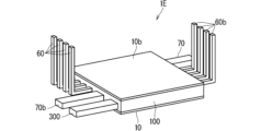
- Fig. 13 is a schematic perspective view showing an example of the semiconductor device 1E. In Fig. 13, the thicknesses of some of the components of the semiconductor device 1E are changed compared to Fig. 12.
- the semiconductor device 1E is a semiconductor device 1A that is provided with an additional configuration 210b, which is the same as the configuration 210 consisting of the base plate 10, insulating substrate 20, conductive pattern 30, semiconductor element 40, bonding materials 90, 91, 92, and integral member 50, an external terminal 300, and a wiring member 310.
- the base plate 10, insulating substrate 20, conductive pattern 30, semiconductor element 40, bonding materials 90, 91, 92, and integral member 50 that constitute the additional configuration 210b will be referred to as the base plate 10b, insulating substrate 20b, conductive pattern 30b, semiconductor element 40b, bonding materials 90b, 91b, 92b, and integral member 50b, respectively.
- main electrode 41, main electrode 42, and signal electrode 45 provided on the semiconductor element 40b will be referred to as the main electrode 41b, main electrode 42b, and signal electrode 45b, respectively.
- signal terminal 60, main terminal 70, and insulating member 80 included in the integrated member 50b are referred to as the signal terminal 60b, main terminal 70b, and insulating member 80b, respectively.
- Both the signal terminal 60 of the configuration 210 and the signal terminal 60b of the configuration 210b are bent upward. Otherwise, the configurations 210 and 210b are arranged symmetrically in the vertical and horizontal directions.
- the configuration consisting of the base plate 10b, insulating substrate 20b, conductive pattern 30b, semiconductor element 40b, bonding materials 90b, 91b, 92b, main terminal 70b, and horizontal portions of the signal terminal 60b of the configuration 210b is located above the configuration consisting of the base plate 10, insulating substrate 20, conductive pattern 30, semiconductor element 40, bonding materials 90, 91, 92, main terminal 70, and horizontal portions of the signal terminal 60 of the configuration 210.
- the sealing material 100 is located between the base plate 10 and the base plate 10b.
- the insulating substrate 20b, the conductive pattern 30b, the semiconductor element 40b, the bonding materials 90b, 91b, 92b, and the integrated member 50b of the configuration 210b, the external terminal 300, and the wiring member 310 are covered with the sealing material 100.
- a part of the main terminal 70b of the integrated member 50b, a part of the signal terminal 60b of the integrated member 50b, and a part of the external terminal 300 are taken out to the outside of the sealing material 100.
- the wiring member 310 electrically connects the main terminal 70 of the component 210 and the conductive pattern 30b of the component 210b.
- the wiring member 310 is, for example, a long and thin plate-shaped member (in other words, a rod-shaped member).
- the wiring member 310 extends in the vertical direction.
- the wiring member 310 is made of a conductive material.
- the material of the wiring member 310 may be a metal such as copper or aluminum.
- the lower end of the wiring member 310 is joined to the upper surface of the main terminal 70 of the component 210 with a conductive bonding material such as solder or brazing material.
- the upper end of the wiring member 310 is joined to the conductive pattern 30b of the component 210b with a conductive bonding material such as solder or brazing material.
- the external terminal 300 is, for example, a long and thin plate-like member (in other words, a rod-like member).
- One longitudinal end of the external terminal 300 is joined to the upper surface of the conductive pattern 30 of the configuration 210 with a conductive joining material such as solder or brazing material.
- the external terminal 300 extends slightly to the left from the conductive pattern 30 and then bends upward, and then bends to the left and extends outside the sealing material 100. Note that the shape and arrangement of the external terminal 300 are not limited to this.
- the external terminal 300, the signal terminal 60 of the component 210, and the main terminal 70b of the component 210b are taken out from the left side of the sealing material 100. As shown in FIG. 13, on the outside of the sealing material 100, the signal terminal 60 of the component 210, the main terminal 70b of the component 210b, and the external terminal 300 are lined up in the front-to-rear direction in that order from the rear side.
- the main terminal 70 of the component 210 and the signal terminal 60b of the component 210b are taken out from the right side of the sealing material 100. Then, as shown in FIG. 13, on the outside of the sealing material 100, the main terminal 70 of the component 210 and the signal terminal 60b of the component 210b are lined up in the front-to-rear direction. On the outside of the sealing material 100, the main terminal 70 is located behind the signal terminal 60b.
- the wiring member 310 electrically connects the main terminal 70 of the configuration 210 and the conductive pattern 30b of the configuration 210b, thereby electrically connecting the main electrode 41 of the lower semiconductor element 40 and the main electrode 42b of the upper semiconductor element 40b to each other. Furthermore, the external terminal 300 is joined to the conductive pattern 30, thereby electrically connecting the external terminal 300 and the main electrode 42 of the lower semiconductor element 40 to each other. As a result, a main current flows through the external terminal 300.
- the external terminal 300 can also be referred to as a main terminal, for example.
- the external terminal 300 may be referred to as the main terminal 300.
- the semiconductor device 1E having the above configuration can form a leg circuit for one phase in which two switching elements of an inverter circuit that drives a three-phase motor are connected in series.
- the semiconductor elements 40 and 40b are equipped with switching elements such as IGBTs.
- the main electrode 41 of the lower semiconductor element 40 and the main electrode 42b of the upper semiconductor element 40b are electrically connected to each other, so that, for example, the switching element of the semiconductor element 40 and the switching element of the semiconductor element 40b are connected in series, and a leg circuit is formed by the switching element of the semiconductor element 40 and the switching element of the semiconductor element 40b.
- a positive potential is applied to the main terminal 300 electrically connected to the main electrode 42 (e.g., collector electrode) of the lower semiconductor element 40
- a negative potential is applied to the main terminal 70b electrically connected to the main electrode 41b (e.g., emitter electrode) of the upper semiconductor element 40b.
- the main terminal 300 is also called a positive terminal or P terminal
- the main terminal 70b is also called a negative terminal or N terminal.
- the main terminal 70 which is electrically connected to the main electrode 41 of the lower semiconductor element 40 and the main electrode 42b of the upper semiconductor element 40b, is electrically connected to one of the U terminal, V terminal, and W terminal of the three-phase motor.
- the main terminal 70 is also called an output terminal.
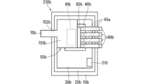
- FIG. 14 is a schematic diagram showing an example of the configuration 210, main terminal 300, and wiring member 310 shown in FIG. 12 viewed from above in a plan view.
- FIG. 15 is a schematic diagram showing an example of the configuration 210b and wiring member 310 shown in FIG. 12 viewed from below in a plan view.
- the main terminal 70b has the same shape as the main terminal 70.
- the main terminal 70b has a wide portion 701b and a narrow portion 702b.
- the narrow portion 702b extends to the right from the wide portion 701b and is taken out to the outside of the sealing material 100.
- the semiconductor element 40 and the semiconductor element 40b are arranged so as to be offset from each other in the horizontal direction. Therefore, when the semiconductor device 1E is viewed in a plan view from the top and bottom, the entire area of the semiconductor element 40 and the entire area of the semiconductor element 40b do not overlap each other, but a part of the semiconductor element 40 and a part of the semiconductor element 40b overlap each other.
- the semiconductor element 40 and the semiconductor element 40b are arranged so as to be offset from each other in the left-right direction and the front-back direction.
- the upper integrated member 50b partially overlaps with the lower semiconductor element 40
- the lower integrated member 50 partially overlaps with the upper semiconductor element 40b.
- the positions of the base plates 10 and 10b in the left-right and front-back directions are the same, the positions of the insulating substrate 20 and insulating substrate 20b in the left-right and front-back directions are the same, and the positions of the conductive patterns 30 and 30b in the left-right and front-back directions are the same. Therefore, when the semiconductor device 1E is seen through a plan view from the top and bottom, the entire area of the base plate 10 and the entire area of the base plate 10b overlap with each other, the entire area of the insulating substrate 20 and the entire area of the insulating substrate 20a overlap with each other, and the entire area of the conductive pattern 30 and the entire area of the conductive pattern 30a overlap with each other.
- the base plates 10 and 10b may partially overlap each other.
- the conductive patterns 30 and 30a may partially overlap each other.
- the semiconductor elements 40 and 40a may partially overlap each other.
- the semiconductor element 40b is located on the opposite side of the semiconductor element 40 (the upper side in this example) with respect to the signal terminals 60 and main terminals 70 to which the semiconductor element 40 is joined. This makes it possible to reduce the footprint of the semiconductor device 1E compared to a case in which the semiconductor element 40b is located on the same side as the semiconductor element 40 (the lower side in this example) with respect to the signal terminals 60 and main terminals 70 and the semiconductor elements 40 and 40b are arranged horizontally.
- the wiring member 310 that is joined to the conductive pattern 30b and the main terminal 70 can be shortened. This point will be explained below.
- the surface (called the main surface) that is bonded to the conductive pattern 30b is called the first surface
- the surface (also called the main surface) that is bonded to the signal terminal 60b and the main terminal 70b is called the second surface.
- the second surface opposite to the first surface is located on the semiconductor element 40 side (lower side in this example).
- the conductive pattern 30b bonded to the first surface of the semiconductor element 40b is located closer to the main terminal 70 than the insulating substrate 20b. Therefore, when bonding the wiring member 310 to the conductive pattern 30b and the main terminal 70, the insulating substrate 20b is less likely to get in the way. In other words, the wiring member 310 does not need to avoid the insulating substrate 20b, and the wiring member 310 can be shortened.
- a plating layer may be provided in the area where the semiconductor element 40 is bonded on at least one of the signal terminal 60 and the main terminal 70. Also, a plating layer may be provided in the area where the semiconductor element 40b is bonded on at least one of the signal terminal 60b and the main terminal 70b.
- integral member 50C provided in semiconductor device 1C may be used instead of integral member 50, and integral member 50C may be used instead of integral member 50b.
- 1A, 1B, 1C, 1D semiconductor device, 20, 20a, 20b: insulating substrate, 30, 30a, 30b: conductive pattern, 40, 40a, 40b: semiconductor element, 50, 50b, 50C: integrated member, 60, 60a, 60b, 60C, 70, 300: external terminal, 91, 92: bonding material, 100: sealing material, 110, 120: plating layer, 160: internal part, 161: external part, 310: wiring member.
Landscapes
- Lead Frames For Integrated Circuits (AREA)
- Structures Or Materials For Encapsulating Or Coating Semiconductor Devices Or Solid State Devices (AREA)
Priority Applications (3)
| Application Number | Priority Date | Filing Date | Title |
|---|---|---|---|
| CN202380102001.4A CN121816872A (zh) | 2023-09-11 | 2023-09-11 | 半导体装置及半导体装置的制造方法 |
| JP2025545315A JPWO2025057268A1 (https=) | 2023-09-11 | 2023-09-11 | |
| PCT/JP2023/033050 WO2025057268A1 (ja) | 2023-09-11 | 2023-09-11 | 半導体装置及び半導体装置の製造方法 |
Applications Claiming Priority (1)
| Application Number | Priority Date | Filing Date | Title |
|---|---|---|---|
| PCT/JP2023/033050 WO2025057268A1 (ja) | 2023-09-11 | 2023-09-11 | 半導体装置及び半導体装置の製造方法 |
Publications (1)
| Publication Number | Publication Date |
|---|---|
| WO2025057268A1 true WO2025057268A1 (ja) | 2025-03-20 |
Family
ID=95021824
Family Applications (1)
| Application Number | Title | Priority Date | Filing Date |
|---|---|---|---|
| PCT/JP2023/033050 Pending WO2025057268A1 (ja) | 2023-09-11 | 2023-09-11 | 半導体装置及び半導体装置の製造方法 |
Country Status (3)
| Country | Link |
|---|---|
| JP (1) | JPWO2025057268A1 (https=) |
| CN (1) | CN121816872A (https=) |
| WO (1) | WO2025057268A1 (https=) |
Citations (4)
| Publication number | Priority date | Publication date | Assignee | Title |
|---|---|---|---|---|
| JPH06338584A (ja) * | 1993-05-31 | 1994-12-06 | Nec Corp | 半導体装置 |
| JP2005150596A (ja) * | 2003-11-19 | 2005-06-09 | Nissan Motor Co Ltd | 半導体装置及びその製造方法 |
| JP2005302951A (ja) * | 2004-04-09 | 2005-10-27 | Toshiba Corp | 電力用半導体装置パッケージ |
| JP2008210942A (ja) * | 2007-02-26 | 2008-09-11 | Fuji Electric Device Technology Co Ltd | 半導体装置およびその製造方法 |
-
2023
- 2023-09-11 WO PCT/JP2023/033050 patent/WO2025057268A1/ja active Pending
- 2023-09-11 JP JP2025545315A patent/JPWO2025057268A1/ja active Pending
- 2023-09-11 CN CN202380102001.4A patent/CN121816872A/zh active Pending
Patent Citations (4)
| Publication number | Priority date | Publication date | Assignee | Title |
|---|---|---|---|---|
| JPH06338584A (ja) * | 1993-05-31 | 1994-12-06 | Nec Corp | 半導体装置 |
| JP2005150596A (ja) * | 2003-11-19 | 2005-06-09 | Nissan Motor Co Ltd | 半導体装置及びその製造方法 |
| JP2005302951A (ja) * | 2004-04-09 | 2005-10-27 | Toshiba Corp | 電力用半導体装置パッケージ |
| JP2008210942A (ja) * | 2007-02-26 | 2008-09-11 | Fuji Electric Device Technology Co Ltd | 半導体装置およびその製造方法 |
Also Published As
| Publication number | Publication date |
|---|---|
| CN121816872A (zh) | 2026-04-07 |
| JPWO2025057268A1 (https=) | 2025-03-20 |
Similar Documents
| Publication | Publication Date | Title |
|---|---|---|
| US6072240A (en) | Semiconductor chip package | |
| US9673118B2 (en) | Power module and method of manufacturing power module | |
| CN103426861B (zh) | 功率半导体的可靠区域接合件 | |
| JP4438489B2 (ja) | 半導体装置 | |
| KR101759398B1 (ko) | 반도체 장치와 그 제조 방법 | |
| JP7411849B2 (ja) | 半導体モジュール | |
| US20050218494A1 (en) | Semiconductor device, a method of manufacturing the same and an electronic device | |
| JP4254527B2 (ja) | 半導体装置 | |
| CN111354709B (zh) | 半导体装置及其制造方法 | |
| US12476161B2 (en) | Semiconductor package with lead frame | |
| JP7459465B2 (ja) | 半導体装置及び半導体装置の製造方法 | |
| US20140084438A1 (en) | Semiconductor device and method of manufacturing same | |
| WO2021210402A1 (ja) | 半導体装置 | |
| US9859195B1 (en) | Semiconductor device | |
| CN112106194A (zh) | 用于半导体功率模块的排热组件 | |
| JP7354464B2 (ja) | 半導体モジュール | |
| US20180174998A1 (en) | Method for manufacturing semiconductor device | |
| JP2009141288A (ja) | 電力用半導体モジュール | |
| JP7524559B2 (ja) | 配線構造及び半導体モジュール | |
| WO2025057268A1 (ja) | 半導体装置及び半導体装置の製造方法 | |
| JP7543854B2 (ja) | 半導体装置及び半導体装置の製造方法 | |
| JP2016225365A (ja) | パワー半導体装置 | |
| JP7035868B2 (ja) | 半導体装置 | |
| JP7147186B2 (ja) | 半導体装置 | |
| JP7678934B1 (ja) | 半導体装置 |
Legal Events
| Date | Code | Title | Description |
|---|---|---|---|
| 121 | Ep: the epo has been informed by wipo that ep was designated in this application |
Ref document number: 23952165 Country of ref document: EP Kind code of ref document: A1 |
|
| ENP | Entry into the national phase |
Ref document number: 2025545315 Country of ref document: JP Kind code of ref document: A |
|
| WWE | Wipo information: entry into national phase |
Ref document number: 2025545315 Country of ref document: JP |