WO2025041264A1 - Spectromètre, système de mesure d'épaisseur, dispositif de calcul d'épaisseur, procédé de production de spectromètre et procédé de calcul d'épaisseur - Google Patents
Spectromètre, système de mesure d'épaisseur, dispositif de calcul d'épaisseur, procédé de production de spectromètre et procédé de calcul d'épaisseur Download PDFInfo
- Publication number
- WO2025041264A1 WO2025041264A1 PCT/JP2023/030153 JP2023030153W WO2025041264A1 WO 2025041264 A1 WO2025041264 A1 WO 2025041264A1 JP 2023030153 W JP2023030153 W JP 2023030153W WO 2025041264 A1 WO2025041264 A1 WO 2025041264A1
- Authority
- WO
- WIPO (PCT)
- Prior art keywords
- surface layer
- thickness
- layer
- round
- internal transmittance
- Prior art date
- Legal status (The legal status is an assumption and is not a legal conclusion. Google has not performed a legal analysis and makes no representation as to the accuracy of the status listed.)
- Pending
Links
Images


Classifications
-
- G—PHYSICS
- G01—MEASURING; TESTING
- G01B—MEASURING LENGTH, THICKNESS OR SIMILAR LINEAR DIMENSIONS; MEASURING ANGLES; MEASURING AREAS; MEASURING IRREGULARITIES OF SURFACES OR CONTOURS
- G01B11/00—Measuring arrangements characterised by the use of optical techniques
- G01B11/02—Measuring arrangements characterised by the use of optical techniques for measuring length, width or thickness
- G01B11/06—Measuring arrangements characterised by the use of optical techniques for measuring length, width or thickness for measuring thickness ; e.g. of sheet material
Definitions
- the present invention relates to a spectrometer, a thickness measurement system, a thickness calculation device, a method for manufacturing a spectrometer, and a method for calculating thickness.
- Patent Document 1 JP Patent Publication 2014-55780A discloses a film thickness measurement method as follows. That is, the film thickness measurement method uses a sample including a reference film having a first wavelength region and a second wavelength region with a difference in light transmittance, the first wavelength region having a lower light transmittance than the second wavelength region, one or more measurement target films formed on one side of the reference film, and one or more measurement target films formed on the other side of the reference film, and measures the thickness of each of the measurement target films, and includes an irradiation step of irradiating the sample with light from the one side, a measurement step of measuring the reflectance spectrum of the light by the sample in part or all of the first wavelength region and part or all of the second wavelength region, a first calculation step of calculating the thickness of each of the measurement target films formed on the one side based on the reflectance spectrum in the first wavelength region, and a second calculation step of calculating the thickness of each of the films formed on the other side based on the thickness of each of the measurement
- Patent Document 2 JP 2008-286583 A discloses an optical property measuring device equipped with a Cassegrain-type reflective objective lens.
- the reflective objective lens includes a convex reflector and a concave reflector arranged so that the central axis coincides with the optical axis.
- the optical property measuring device described in Patent Document 2 the measurement reflected light generated by reflection from the surface of the object to be measured passes through a pinhole and enters the spectroscopic measurement unit, while the back-reflected light generated by reflection from the back surface of the object to be measured cannot pass through the pinhole. Therefore, the optical property measuring device described in Patent Document 2 can avoid the effects of back-reflected light, i.e., stray light.
- the present invention has been made to solve the above-mentioned problems, and its purpose is to provide a spectrometer, a thickness measurement system, a thickness calculation device, a method for manufacturing a spectrometer, and a thickness calculation method that are capable of more accurately measuring the thickness of the surface layer of a target sample with a multi-layer structure.
- a spectrometer used to measure the thickness of a surface layer of a target sample having a multilayer structure in which a surface layer and an underlayer are stacked, and includes a light receiving section that receives light reflected from the target sample of light irradiated from the surface layer side of the target sample, and a spectroscopic section that generates a reflected light spectrum by dispersing the reflected light, and the spectroscopic section generates the reflected light spectrum in a spectral wavelength range in which the round-trip internal transmittance of the surface layer is equal to or greater than a predetermined lower limit, and the round-trip internal transmittance of the layer consisting of the surface layer and the underlayer is equal to or less than a predetermined upper limit.
- a reflected light spectrum can be generated that includes the components of reflected light at the light-irradiated surface of the surface layer and the components of reflected light at the interface between the surface layer and the lower layer, while reducing the components of reflected light at the interface on the opposite side of the interface in the lower layer.
- the thickness of the surface layer can be calculated more accurately based on the reflectance spectrum, which is the interference waveform of the surface layer generated using the reflected light spectrum. Therefore, the thickness of the surface layer in a target sample with a multilayer structure can be measured more accurately.
- the "round-trip internal transmittance I(d)" corresponds to the component of light incident on a layer of thickness d that is reflected at the interface opposite to the incident surface, i.e., the back surface, and returns to the incident surface, and is the attenuation due to material absorption in the round-trip process in the layer expressed as transmittance.
- the spectroscopic unit may generate the reflected light spectrum in the spectroscopic wavelength range in which, within the thickness range of the surface layer, the round-trip internal transmittance of the surface layer is equal to or greater than a predetermined threshold, and the round-trip internal transmittance of the combined layer of the surface layer and the lower layer is equal to or less than the threshold.
- a reflected light spectrum that is more effective in thickness measurement, taking into account detection limits based on noise, dynamic range, etc.
- This configuration allows for more accurate measurement of the thickness of the silicon layer that constitutes the main surface of the multi-layer structure.
- a thickness measurement system includes a spectrometer as described above in (1) to (3), and a macro-optical system that irradiates the surface layer side of the target sample with light from a light source and guides the reflected light from the target sample to the spectrometer.
- This configuration allows the thickness of the surface layer to be measured more quickly than a microspectrophotometer such as the optical property measuring device described in Patent Document 2.
- a thickness calculation device used to measure the thickness of a surface layer of a target sample having a multilayer structure in which a surface layer and a lower layer are stacked, and includes an acquisition unit that acquires a reflected light spectrum of light reflected from the target sample by light irradiated from the surface layer side of the target sample, a generation unit that generates a reflectance spectrum of the target sample based on the reflected light spectrum acquired by the acquisition unit, and a calculation unit that calculates the thickness of the surface layer based on the reflectance spectrum generated by the generation unit, and the generation unit generates the reflectance spectrum in a wavelength range in which the round-trip internal transmittance of the surface layer is equal to or greater than a predetermined lower limit and the round-trip internal transmittance of the layer consisting of the surface layer and the lower layer is equal to or less than a predetermined upper limit.
- a reflectance spectrum is generated in a wavelength range where the round-trip internal transmittance of the surface layer is equal to or greater than a predetermined lower limit and the round-trip internal transmittance of the combined surface layer and lower layer is equal to or less than an upper limit based on the reflected light spectrum of the reflected light of the target sample, and the thickness is calculated based on the reflectance spectrum.
- This makes it possible to generate a reflectance spectrum that includes components of reflected light at the light-irradiated surface of the surface layer and components of reflected light at the interface between the surface layer and the lower layer, while reducing components of reflected light at the interface of the lower layer on the opposite side to the interface. Therefore, the thickness of the surface layer can be calculated more accurately using the generated reflectance spectrum. Therefore, the thickness of the surface layer of a target sample with a multilayer structure can be measured more accurately.
- the generating unit may generate the reflectance spectrum in the wavelength range in which, within the thickness range of the surface layer, the round-trip internal transmittance of the surface layer is equal to or greater than a predetermined threshold, and the round-trip internal transmittance of the layer consisting of the surface layer and the lower layer is equal to or less than the threshold.
- a manufacturing method of a spectrometer is a manufacturing method of a spectrometer used for measuring the thickness of a surface layer of a target sample having a multilayer structure in which a surface layer and a lower layer are stacked, and includes the steps of acquiring first correspondence information indicating the correspondence relationship between a wavelength and a round-trip internal transmittance of the surface layer, acquiring second correspondence information indicating the correspondence relationship between a wavelength and a round-trip internal transmittance of a layer formed by combining the surface layer and the lower layer, and setting a spectroscopic wavelength range of the spectrometer that splits light reflected from the target sample of light irradiated from the surface layer side of the target sample based on the acquired first correspondence information and second correspondence information, and in the step of setting the spectroscopic wavelength range, the spectroscopic wavelength range is set so that the round-trip internal transmittance of the surface layer is equal to or greater than a predetermined
- the thickness of the surface layer can be calculated more accurately using the reflectance spectrum, which is the interference waveform of the surface layer generated using the reflected light spectrum. Therefore, the thickness of the surface layer in a target sample having a multi
- the method of manufacturing the spectrometer may further include a step of acquiring a thickness range of the surface layer, and in the step of setting the spectroscopic wavelength range, the spectroscopic wavelength range may be set within a wavelength range between a first wavelength, which is the wavelength at which the round-trip internal transmittance of the surface layer reaches a predetermined threshold value when the thickness of the surface layer is the maximum value of the thickness range, and a second wavelength, which is the wavelength at which the round-trip internal transmittance of the combined layer of the surface layer and the underlayer reaches the threshold value when the thickness of the surface layer is the minimum value of the thickness range.
- a first wavelength which is the wavelength at which the round-trip internal transmittance of the surface layer reaches a predetermined threshold value when the thickness of the surface layer is the maximum value of the thickness range
- a second wavelength which is the wavelength at which the round-trip internal transmittance of the combined layer of the surface layer and the underlayer reaches the threshold value when the thickness of the surface layer is the minimum value of the
- a spectrometer capable of generating a reflected light spectrum that is more effective in thickness measurement, taking into account detection limits based on noise, dynamic range, etc.
- the specifications of a spectrometer capable of generating a reflected light spectrum in which the level of reflected light reflected at the interface between the surface layer and the lower layer is equal to or higher than the noise level, and the level of reflected light reflected at the interface between the lower layer and another lower layer is equal to or lower than the noise level.
- a thickness calculation method is a thickness calculation method in a thickness calculation device used to measure the thickness of a surface layer of a target sample having a multilayer structure in which a surface layer and an underlayer are stacked, and includes the steps of acquiring a reflected light spectrum of light reflected from the target sample, the light being irradiated from the surface layer side of the target sample, generating a reflectance spectrum of the target sample based on the acquired reflected light spectrum, and calculating the thickness of the surface layer based on the generated reflectance spectrum, and in the step of generating the reflectance spectrum, the reflectance spectrum is generated in a wavelength range in which the round-trip internal transmittance of the surface layer is equal to or greater than a predetermined lower limit, and the round-trip internal transmittance of the combined layer of the surface layer and the underlayer is equal to or less than a predetermined upper limit.
- the thickness of the surface layer can be calculated more accurately using the generated reflectance spectrum. Therefore, the thickness of the surface layer of a target sample with a multilayer structure can be measured more accurately.
- the present invention makes it possible to more accurately measure the thickness of the surface layer of a multi-layered target sample.
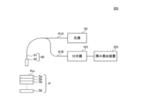
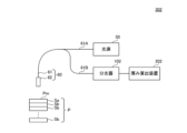
- FIG. 1 is a diagram showing the configuration of a thickness measurement system according to a first embodiment of the present invention.
- FIG. 2 is a diagram showing a configuration of a thickness calculation device according to the first embodiment of the present invention.
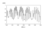
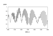
- FIG. 3 is a diagram showing a simulation result of thickness measurement of a target sample by a thickness measurement system according to a comparative example.
- FIG. 4 is a diagram showing a simulation result of thickness measurement of a target sample by a thickness measurement system according to a comparative example.
- FIG. 5 is a diagram showing a simulation result of thickness measurement of a target sample by a thickness measurement system according to a comparative example.
- FIG. 6 is a diagram showing a simulation result of thickness measurement of a target sample by a thickness measurement system according to a comparative example.
- FIG. 1 is a diagram showing the configuration of a thickness measurement system according to a first embodiment of the present invention.
- FIG. 2 is a diagram showing a configuration of a thickness calculation device according to the first embodiment of
- FIG. 7 is a diagram showing a simulation result of thickness measurement of a target sample by a thickness measurement system according to a comparative example.
- FIG. 8 is a diagram showing a simulation result of thickness measurement of a target sample by the thickness measurement system according to the comparative example.
- FIG. 9 is a diagram showing the configuration of a spectrometer according to the first embodiment of the present invention.
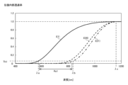
- FIG. 10 is a diagram showing the simulation results of the round-trip internal transmittance of the surface layer.
- FIG. 11 is a diagram showing the extinction coefficient of silicon.
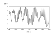
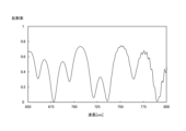
- FIG. 12 shows a reflectance spectrum SR generated in the thickness measurement system according to the first embodiment of the present invention.
- FIG. 13 shows a reflectance spectrum SR generated in the thickness measurement system according to the first embodiment of the present invention.
- FIG. 14 shows a reflectance spectrum SR generated in the thickness measurement system according to the first embodiment of the present invention.
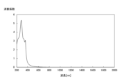
- FIG. 15 shows a power spectrum generated in the thickness measurement system according to the first embodiment of the present invention.
- FIG. 16 shows a power spectrum generated in the thickness measurement system according to the first embodiment of the present invention.
- FIG. 17 shows a power spectrum generated in the thickness measurement system according to the first embodiment of the present invention.
- FIG. 18 is a flowchart showing a method for manufacturing a spectroscope in the thickness measurement system according to the first embodiment of the present invention.
- FIG. 19 is a diagram showing a configuration of a thickness measurement system according to the second embodiment of the present invention.
- FIG. 20 is a diagram showing a configuration of a thickness calculation device according to the second embodiment of the present invention.
- FIG. 21 is a flowchart defining an example of an operational procedure when the thickness calculation device according to the second embodiment of the present invention calculates the thickness of a surface layer.
- First Embodiment 1 is a diagram showing a configuration of a thickness measurement system according to a first embodiment of the present invention.
- the thickness measurement system 301 includes a light source 50, a macro optical system 60, a spectroscope 101, and a thickness calculation device 201.
- the thickness measurement system 301 is a spectral interference type measurement system, and is used to measure the thickness of a surface layer Sa in a target sample P having a multilayer structure in which a surface layer Sa and a lower layer Sb are laminated.
- the surface of the surface layer Sa is the main surface Pm of the target sample P.
- the lower limit of the thickness range Rth of the surface layer Sa to be measured is 1 ⁇ m or more, and the upper limit of the thickness range Rth is 20 ⁇ m or less.
- the shape of the target sample P may be a wafer shape, a rectangular shape, or a film shape.
- the target sample P includes a surface layer Sa and multiple lower layers Sb.
- the surface layer Sa is a silicon layer
- the lower layers Sb are silicon layers coated with a silicon oxide thin film.
- the target sample P has a repeating layer structure in which multiple silicon layers coated with a silicon oxide thin film are stacked as the lower layers Sb from the surface layer Sa side.
- the target sample P has a repeating layer structure in which a silicon oxide layer, which is a coating, and a silicon layer are alternately stacked as the lower layers Sb from the surface layer Sa side.
- the target sample P may be configured to include one lower layer Sb.
- the lower layer Sb adjacent to the surface layer Sa i.e., the lower layer Sb directly below the surface layer Sa, is also referred to as the "adjacent lower layer Sb".
- the light source 50 emits light used to measure the thickness of the surface layer Sa.
- the light source 50 emits light including multiple wavelengths.
- the spectrum of the light emitted by the light source 50 is a continuous spectrum.
- the range of wavelengths of the light emitted by the light source 50 includes the spectral wavelength range Rs1 of the spectroscope 101.
- the light source 50 is, for example, a halogen lamp.
- the macro optical system 60 irradiates the surface layer Sa side of the target sample P with light from the light source 50, and guides the reflected light of the irradiated light from the target sample P to the spectrometer 101. More specifically, the macro optical system 60 includes a Y-type optical fiber 61 and a probe 62. The probe 62 is provided at a first end of the Y-type optical fiber 61. The second end of the Y-type optical fiber 61 is bifurcated. The branched portion 61A of the Y-type optical fiber 61 is connected to the light source 50. The branched portion 61B of the Y-type optical fiber 61 is connected to the spectrometer 101.
- the light emitted from the light source 50 is irradiated onto the main surface Pm of the target sample P via the Y-type optical fiber 61 and the probe 62.
- the reflected light from the target sample P of the light irradiated onto the main surface Pm is guided to the spectrometer 101 via the probe 62 and the Y-type optical fiber 61.
- the thickness measurement system 301 may be configured to include an optical system including a lens, a beam splitter, etc., instead of the macro optical system 60.
- the spectrometer 101 generates a reflected light spectrum SL including a spectroscopic wavelength range Rs1 by dispersing the reflected light from the target sample P.
- the spectrometer 101 generates a reflected light spectrum SL in the spectroscopic wavelength range Rs1 by dispersing the reflected light from the target sample P.
- the spectrometer 101 transmits the generated reflected light spectrum SL to the thickness calculation device 201.
- FIG. 2 is a diagram showing the configuration of a thickness calculation device according to a first embodiment of the present invention.
- the thickness calculation device 201 includes a receiving unit 21, a generating unit 22, and a calculating unit 23.
- the receiving unit 21 is an example of an acquisition unit.
- the receiving unit 21, the generating unit 22, and a part or all of the calculating unit 23 are realized, for example, by a processing circuit including one or more processors.
- the receiver 21 receives from the spectrometer 101 the reflected light spectrum SL from the target sample P irradiated with light from the surface layer Sa side, and outputs the received reflected light spectrum SL to the generator 22.
- the generating unit 22 generates a reflectance spectrum SR of the target sample P based on the reflected light spectrum SL received from the receiving unit 21. More specifically, the generating unit 22 generates the reflectance spectrum SR by dividing the reflected light spectrum SL by the irradiated light spectrum of the light irradiated to the target sample P. The generating unit 22 outputs the generated reflectance spectrum SR to the calculating unit 23.
- the calculation unit 23 calculates the thickness of the surface layer Sa based on the reflectance spectrum SR generated by the generation unit 22. For example, the calculation unit 23 calculates the thickness of the surface layer Sa by analyzing the reflectance spectrum SR according to the FFT (Fast Fourier Transform) method. More specifically, the calculation unit 23 generates a power spectrum of the reflectance spectrum SR by performing FFT processing on the reflectance spectrum SR. Then, the calculation unit 23 identifies a thickness that meets the given selection conditions from the generated power spectrum as the thickness of the surface layer Sa.
- FFT Fast Fourier Transform
- a reflectance spectrum SR in a wavelength range in which the internal transmittance of the film is high by dispersing light reflected from the film when light is irradiated from the outside onto the main surface of the film, and to calculate the thickness based on the reflectance spectrum SR.
- a conventional thickness measurement system when measuring the thickness of a silicon film, for example, a conventional thickness measurement system generates a reflected light spectrum SL using a spectrometer with a spectral wavelength range of 1000 nm or more, where the extinction coefficient of the silicon film is close to zero, and calculates the thickness of the silicon layer based on the generated reflected light spectrum SL.
- Figures 3 to 8 show the simulation results of thickness measurement of a target sample using a thickness measurement system according to a comparative example.
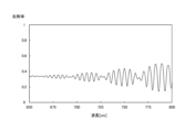
- Figures 3 to 5 show reflectance spectra SR generated in a comparative thickness measurement system equipped with a spectrometer having a spectral wavelength range of 1000 nm or more and sufficient wavelength resolution.
- the horizontal axis is wavelength [nm] and the vertical axis is reflectance.
- Figure 3 shows the reflectance spectrum SR of a target sample P1 that includes a 1 ⁇ m silicon layer as a surface layer Sa and includes six alternating layers of 5 ⁇ m silicon oxide layers and 21 ⁇ m silicon layers from the surface layer Sa side as lower layers Sb.
- Figure 4 shows the reflectance spectrum SR of a target sample P2 that includes a 10 ⁇ m silicon layer as a surface layer Sa compared to the target sample P1.
- Figure 5 shows the reflectance spectrum SR of a target sample P3 that includes a 20 ⁇ m silicon layer as a surface layer Sa compared to the target sample P1.
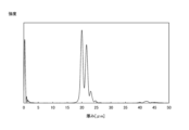
- FIGS. 6 to 8 show power spectra generated in a thickness measurement system according to a comparative example.
- the horizontal axis represents thickness [ ⁇ m] and the vertical axis represents intensity.
- FIG. 6 to FIG. 8 show the power spectra of the reflectance spectrum SR shown in FIG. 3 to FIG. 5, respectively.
- the thickness measurement system according to the comparative example cannot accurately measure the thickness of the surface layer Sa of the target sample P1. More specifically, in the power spectra of the target samples P1, P2, and P3 generated by the thickness measurement system according to the comparative example, the thickness corresponding to the maximum intensity is approximately 2 ⁇ m. Therefore, the measurement result of the thickness of the surface layer Sa by the thickness measurement system according to the comparative example is approximately 2 ⁇ m, even though the actual thickness of the surface layer Sa is 1 ⁇ m, 10 ⁇ m, or 20 ⁇ m.
- the thickness of the target samples P1, P2, and P3 having a multilayer structure is measured using the thickness measurement system according to the comparative example, it is difficult to measure the thickness of the surface layer Sa. Furthermore, even if the reflectance spectrum SR could be separated into layers, it is difficult to identify which layer the thickness calculated based on the reflectance spectrum SR indicates.
- Patent Document 1 requires that the substrate film has a transmittance in a specified wavelength band that is smaller than that of the coating film, and measurements cannot be made if the coating film has a smaller transmittance than the substrate film. Furthermore, with the technology described in Patent Document 1, when multiple layers are stacked on one side of the substrate film, it is not possible to measure the thickness of the surface layer of the multiple layers.
- Patent Document 2 also describes a technique for suppressing light from the back surface of the object being measured from appearing as stray light by using a Cassegrain-type reflective objective lens.
- the technique described in Patent Document 2 has significant design constraints.
- the thickness measurement system 301 solves the above problems by adopting the following configuration.
- Fig. 9 is a diagram showing the configuration of a spectrometer according to a first embodiment of the present invention.
- spectrometer 101 includes slit 11 and spectroscopic section 12.
- Spectroscopic section 12 includes diffraction grating 12A, detection section 12B, collimator mirror 12C, and focus mirror 12D.
- Slit 11 is an example of a light receiving section.
- the slit 11 receives the reflected light from the target sample P of the light irradiated from the surface layer Sa side of the target sample P. More specifically, the slit 11 receives the reflected light from the target sample P via the branching portion 61B of the Y-shaped optical fiber 61. The reflected light from the target sample P that enters the inside of the spectroscope 101 from the slit 11 is collimated by the collimating mirror 12C.
- the spectroscopic unit 12 generates a reflected light spectrum SL by dispersing the reflected light from the target sample P.
- the light that has been collimated by the collimating mirror 12C is guided to the diffraction grating 12A.
- the diffraction grating 12A separates the incident light into different diffraction angles for each wavelength.
- the light split into different angles for each wavelength by the diffraction grating 12A is focused by the focus mirror 12D at different positions for each wavelength in the detection unit 12B.
- the detection unit 12B is a linear image sensor composed of multiple detection elements arranged in a line.
- detection elements are, for example, a CCD (Charge Coupled Device) image sensor or a CMOS (Complementary Metal Oxide Semiconductor) image sensor.
- CCD Charge Coupled Device
- CMOS Complementary Metal Oxide Semiconductor
- the detection unit 12B generates a reflected light spectrum SL that indicates the relationship between the wavelength and intensity of the light received on the light receiving surface of each detection element, and transmits the generated reflected light spectrum SL to the thickness calculation device 201.
- the wavelength resolution of the reflected light spectrum SL generated by the spectroscopic section 12 satisfies the following expressions (1) and (2).
- R1 is the optical resolution.
- R2 is the pixel resolution.
- ⁇ 1 is the wavelength corresponding to the maximum intensity value M1 in the reflected light spectrum SL.
- ⁇ 2 is the wavelength corresponding to the maximum intensity value M2 in the reflected light spectrum SL.
- Maximum value M2 is a maximum value that is greater than and adjacent to maximum value M1.
- the spectroscopic unit 12 generates a reflected light spectrum SL in a spectroscopic wavelength range Rs1 in which the round-trip internal transmittance Ia(d), which is the round-trip internal transmittance I(d) of the surface layer Sa, is equal to or greater than a predetermined lower limit, and the round-trip internal transmittance Iab(d), which is the round-trip internal transmittance I(d) of the layer consisting of the surface layer Sa and the adjacent lower layer Sb, is equal to or less than a predetermined upper limit.
- the round-trip internal transmittance Iab(d) corresponds to the round-trip internal transmittance of a silicon layer having a thickness equal to the sum of the thickness of the surface layer Sa and the thickness of the silicon layer in the adjacent lower layer Sb.
- FIG. 10 is a diagram showing the simulation results of the round-trip internal transmittance.
- the horizontal axis is the wavelength [nm]
- the vertical axis is the round-trip internal transmittance.
- the solid line in FIG. 10 indicates the round-trip internal transmittance I(1), which is the round-trip internal transmittance I(d) of a 1 ⁇ m silicon layer.
- the dashed line in FIG. 10 indicates the round-trip internal transmittance I(20), which is the round-trip internal transmittance I(d) of a 20 ⁇ m silicon layer.
- the dashed line in FIG. 10 indicates the round-trip internal transmittance I(21), which is the round-trip internal transmittance I(d) of a 21 ⁇ m silicon layer.
- the round-trip internal transmittance I(1) is the round-trip internal transmittance of a 1 ⁇ m silicon layer, so it corresponds to the internal transmittance of a 2 ⁇ m silicon layer.
- the round-trip internal transmittance I(20) is the round-trip internal transmittance of a 20 ⁇ m silicon layer, so it corresponds to the internal transmittance of a 40 ⁇ m silicon layer.
- the round-trip internal transmittance I(21) is the round-trip internal transmittance of a 21 ⁇ m silicon layer, which corresponds to the internal transmittance of a 42 ⁇ m silicon layer.
- the spectroscopic unit 12 generates a reflected light spectrum SL in a spectroscopic wavelength range Rs1 where the round-trip internal transmittance Ia(d) of the surface layer Sa is equal to or greater than a predetermined threshold Th1, and the round-trip internal transmittance Iab(d) of the layer consisting of the surface layer Sa and the adjacent lower layer Sb is equal to or less than the threshold Th1, in the thickness range Rth.
- the threshold Th1 is an example of a lower limit and an example of an upper limit.
- the spectral wavelength range Rs1 is set within the wavelength range between the wavelength ⁇ a when the round-trip internal transmittance Ia(1) of the surface layer Sa becomes the threshold value Th1 and the wavelength ⁇ b when the round-trip internal transmittance Iab(21) of the layer including the surface layer Sa and the adjacent lower layer Sb becomes the threshold value Th1.
- the wavelength ⁇ a is an example of the first wavelength.
- the wavelength ⁇ b is an example of the second wavelength.
- the threshold value Th1 is a value less than 1.
- the threshold value Th1 is, for example, 0.001.
- the spectral wavelength range Rs1 may be set within the wavelength range between the wavelength ⁇ a when the round-trip internal transmittance Ia(1) becomes the threshold value Th1 and the wavelength ⁇ b when the round-trip internal transmittance Iab(21) becomes the threshold value Th2 different from the threshold value Th1.
- the spectroscopic unit 12 generates a reflected light spectrum SL in a spectroscopic wavelength range Rs1 in which the round-trip internal transmittance Ia(d) of the surface layer Sa is equal to or greater than the noise level in the thickness calculation device 201, and the round-trip internal transmittance Iab(d) of the surface layer Sa and the adjacent lower layer Sb combined is equal to or less than the noise level in the thickness calculation device 201, in the thickness range Rth.
- the spectroscopic unit 12 generates a reflected light spectrum SL in a spectroscopic wavelength range Rs1 in which the level of the reflected light that passes through the surface layer Sa and is reflected at the interface between the surface layer Sa and the adjacent lower layer Sb is equal to or greater than the noise level in the thickness calculation device 201, and the level of the reflected light that passes through the surface layer Sa and the adjacent lower layer Sb and is reflected at the interface between the adjacent lower layer Sb and another lower layer Sb is equal to or less than the noise level in the thickness calculation device 201, in the thickness range Rth.
- the spectral wavelength range Rs1 is a wavelength range in which the round-trip internal transmittance Ia(d) is equal to or greater than the noise level in the thickness calculation device 201, and in which a sufficient number of interference waves can be obtained for FFT analysis, and in which the combined round-trip internal transmittance Iab(d) of the surface layer Sa and the adjacent lower layer Sb is equal to or less than the noise level in the thickness calculation device 201.
- the spectral wavelength range Rs1 is a wavelength range in which the absolute value of the change in the round-trip internal transmittance of the surface layer Sa with respect to wavelength is equal to or greater than a predetermined value.
- the spectral wavelength range Rs1 of the spectroscopic section 12 is a wavelength range that does not include wavelengths equal to or greater than the wavelength ⁇ c, where there is almost no change in the round-trip internal transmittance Ia(d) of the surface layer Sa, and does not include the ultraviolet range in which there is almost no transmission.
- the spectral wavelength range Rs1 of the spectroscopic section 12 is a wavelength range that is smaller than the wavelength ⁇ c.
- the spectral wavelength range Rs1 includes at least a portion of the visible light region.
- the spectroscopic wavelength range Rs1 of the spectroscopic unit 12 is a wavelength range in which the absolute value of the amount of change in the extinction coefficient of the material that constitutes the surface layer Sa with respect to wavelength is equal to or greater than a predetermined value.
- the spectroscopic wavelength range Rs1 of the spectroscopic unit 12 is a wavelength range that is shorter than the wavelength at which the decrease in the extinction coefficient of silicon, which is the material that constitutes the surface layer Sa, converges, and does not include a range in which the extinction coefficient is extremely large.
- FIG. 11 is a diagram showing the extinction coefficient of silicon.
- the horizontal axis is wavelength [nm] and the vertical axis is extinction coefficient.
- the designer of the spectrometer 101 performs the following process to determine the specifications. That is, the designer of the spectrometer 101 obtains the extinction coefficient of silicon, which is the material that constitutes the surface layer Sa and the adjacent lower layer Sb.
- the designer of the spectrometer 101 also obtains the thickness range Rth of the surface layer Sa to be measured.
- the thickness range Rth is the range of thicknesses that can be measured by the thickness measurement system 301.
- the designer of the spectrometer 101 may set the thickness range Rth according to the target sample P, or may set the thickness range Rth according to the needs of the user of the thickness measurement system 301. For example, the designer of the spectrometer 101 also obtains the thickness range of the adjacent lower layer Sb.
- the designer of the spectroscope 101 creates correspondence information X1 indicating the correspondence relationship between the wavelength of light incident on the surface layer Sa and the round-trip internal transmittance Ia(d) of the surface layer Sa based on the acquired extinction coefficient and thickness range Rth.
- the designer of the spectroscope 101 also creates correspondence information X2 indicating the correspondence relationship between the wavelength of light incident on the surface layer Sa and the round-trip internal transmittance Iab(d) of the layer including the surface layer Sa and the adjacent lower layer Sb based on the acquired extinction coefficient, thickness range Rth, and thickness of the adjacent lower layer Sb.
- the designer of the spectroscope 101 calculates the round-trip internal transmittance Ia(d) at the lower limit of the thickness range Rth and the round-trip internal transmittance Ia(d) at the upper limit of the thickness range Rth according to the following formula (3).
- d is the thickness of the surface layer Sa
- ⁇ is the absorption coefficient, which is expressed by the following formula (4).
- ⁇ is the wavelength of light irradiated from the light source 50 to the surface layer Sa.
- k( ⁇ ) is the extinction coefficient of light with wavelength ⁇ .
- the designer of the spectrometer 101 sets the spectral wavelength range Rs1, based on the correspondence information X1 and X2, in which the round-trip internal transmittance I(d) of the surface layer Sa is equal to or greater than the threshold value Th1, and the round-trip internal transmittance Iab(d) of the layer consisting of the surface layer Sa and the adjacent lower layer Sb is equal to or less than the threshold value Th1.
- the designer of the spectrometer 101 sets the spectral wavelength range Rs1 within the wavelength range between the wavelength ⁇ a when the round-trip internal transmittance Ia(1) becomes the threshold value Th1, and the wavelength ⁇ b when the round-trip internal transmittance Iab(21) becomes the threshold value Th1, as described above.
- the designer of the spectrometer 101 sets a spectral wavelength range Rs1 based on the correspondence information X1 and X2, in which the round-trip internal transmittance Ia(d) of the surface layer Sa is equal to or greater than the noise level in the thickness calculation device 201, the round-trip internal transmittance Iab(d) of the surface layer Sa and the adjacent lower layer Sb is equal to or less than the noise level in the thickness calculation device 201, and a sufficient number of interference wave numbers of the surface layer Sa are obtained for FFT analysis.
- the spectral wavelength range Rs1 is set so that the round-trip internal transmittance Iab(d) of the surface layer Sa and the adjacent lower layer Sb combined is equal to or less than the noise level in the thickness calculation device 201, and only an interference waveform of a level that does not affect the power spectrum of the FFT analysis of the interference waveform obtained from the surface layer Sa is obtained.
- FIGS. 12 to 14 show reflectance spectra SR generated in a thickness measurement system according to a first embodiment of the present invention.
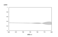
- FIGS. 12 to 14 show reflectance spectra SR generated in a thickness measurement system 301 including a spectrometer 101 having a spectroscopic wavelength range Rs1 of 650 nm or more and 800 nm or less, which is set based on the thickness range Rth of the surface layer Sa.
- the horizontal axis is wavelength [nm]
- the vertical axis is reflectance.
- FIGS. 12 to 14 show reflectance spectra SR of the above-mentioned target samples P1, P2, and P3, respectively.
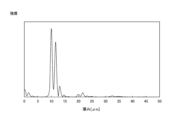
- FIGS. 15 to 17 show power spectra generated in a thickness measurement system according to a first embodiment of the present invention.
- the horizontal axis represents thickness [ ⁇ m] and the vertical axis represents intensity.
- FIG. 15 to FIG. 17 show the power spectra of the reflectance spectrum SR shown in FIG. 12 to FIG. 14, respectively.
- the thickness measurement system 301 can accurately measure the thickness of the surface layer Sa of the target sample P1.
- the thickness corresponding to the maximum intensity is approximately 1 ⁇ m. Therefore, the measurement result of the thickness of the surface layer Sa by the thickness measurement system 301 is approximately equal to the actual thickness of the surface layer Sa.
- the thickness corresponding to the maximum intensity is approximately 10 ⁇ m. Therefore, the measurement result of the thickness of the surface layer Sa by the thickness measurement system 301 is approximately equal to the actual thickness of the surface layer Sa.
- the thickness corresponding to the maximum intensity is approximately 20 ⁇ m. Therefore, the measurement result of the thickness of the surface layer Sa by the thickness measurement system 301 is approximately equal to the actual thickness of the surface layer Sa.
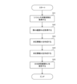
- FIG. 18 is a flowchart showing a method for manufacturing a spectrometer in a thickness measurement system according to a first embodiment of the present invention.
- the designer of the spectrometer 101 performs the following process to determine the specifications.
- the designer of the spectrometer 101 obtains the extinction coefficient of silicon, which is the material that constitutes the surface layer Sa and the adjacent lower layer Sb (step S11).
- the designer of the spectrometer 101 obtains the design values for the thickness range Rth of the surface layer Sa to be measured, and the thickness of the adjacent lower layer Sb (step S12).
- correspondence information X1 that indicates the correspondence between the wavelength of light incident on the surface layer Sa and the round-trip internal transmittance Ia(d) of the surface layer Sa based on the extinction coefficient and the thickness range Rth.
- the correspondence information X1 is information that indicates the wavelength range in which a sufficient number of interference wavenumbers of the surface layer Sa can be obtained for FFT analysis, as well as the spectrometer resolution.
- the designer of the spectrometer 101 calculates the round-trip internal transmittance Ia(1) of the surface layer Sa at the lower limit of the thickness range Rth, and the round-trip internal transmittance Ia(20) of the surface layer Sa at the upper limit of the thickness range Rth (step S13).
- the designer of the spectrometer 101 creates correspondence information X2 that indicates the correspondence between the wavelength of light incident on the surface layer Sa and the round-trip internal transmittance Iab(d) of the layer including the surface layer Sa and the adjacent lower layer Sb, based on the extinction coefficient, the thickness range Rth, and the thickness of the adjacent lower layer Sb. For example, the designer of the spectrometer 101 calculates the round-trip internal transmittance Iab(21) of the surface layer Sa and the adjacent lower layer Sb combined at the lower limit of the thickness range Rth, and the round-trip internal transmittance Iab(40) of the surface layer Sa and the adjacent lower layer Sb combined at the upper limit of the thickness range Rth (step S14).
- the designer of the spectrometer 101 sets a spectroscopic wavelength range Rs1 in which the round-trip internal transmittance Ia(d) of the surface layer Sa is equal to or greater than the threshold value Th1 and the round-trip internal transmittance Iab(d) of the layer consisting of the surface layer Sa and the adjacent lower layer Sb is equal to or less than the threshold value Th1 in the thickness range Rth.
- the designer of the spectrometer 101 sets the spectroscopic wavelength range Rs1 in the wavelength range between the wavelength ⁇ a at which the round-trip internal transmittance Ia(d) is equal to the threshold value Th1 when the thickness of the surface layer Sa is the maximum value of the thickness range Rth, and the wavelength ⁇ b at which the round-trip internal transmittance Iab(d) is equal to the threshold value Th1 when the thickness of the surface layer Sa is the minimum value of the thickness range Rth (step S15).
- step S14 the designer of the spectrometer 101 sets a spectral wavelength range Rs1 that satisfies the conditions that the round-trip internal transmittance Ia(d) is equal to or greater than the noise level in the thickness calculation device 201, and the round-trip internal transmittance Iab(d) of the surface layer Sa and the adjacent lower layer Sb combined is equal to or less than the noise level in the thickness calculation device 201.
- the designer of the spectrometer 101 may set a spectral wavelength range Rs1 that does not satisfy these conditions if the specifications of the thickness measurement system 301 allow it.
- step S14 the designer of the spectrometer 101 sets a spectroscopic wavelength range Rs1 between the wavelength ⁇ a at which the round-trip internal transmittance Ia(d) of the surface layer Sa is equal to or greater than the noise level in the thickness calculation device 201, and the wavelength ⁇ b at which the combined round-trip internal transmittance Iab(d) of the surface layer Sa and the adjacent lower layer Sb is equal to or less than the noise of the measurement device detection unit.
- the designer of the spectrometer 101 may set a spectroscopic wavelength range Rs1 that exceeds the range between the wavelengths ⁇ a and ⁇ b if allowed by the specifications of the thickness measurement system 301.
- step S14 the designer of the spectrometer 101 sets a spectroscopic wavelength range Rs1 that satisfies the condition that the power spectrum obtained by FFT analysis of the interference waveform of the surface layer Sa is sufficiently selectable according to a predetermined selection condition when compared with the power spectrum obtained by FFT analysis of the interference waveform of the adjacent lower layer Sb and the power spectrum obtained by FFT analysis of the interference waveform of the combined layer of the surface layer Sa and the adjacent lower layer Sb.
- the designer of the spectrometer 101 may set a spectroscopic wavelength range Rs1 that does not satisfy this condition if it is permitted by the specifications of the thickness measurement system 301.
- the designer of the spectrometer 101 sets a spectroscopic wavelength range Rs1 and resolution that satisfy the following conditions: when the thickness of the surface layer Sa is assumed to be the lower limit of the thickness range Rth, the wavelength range and resolution satisfy the wavelength range and resolution in which a sufficient number of interference waves can be obtained for analysis in the wavelength range in which the level of the interference waveform of the surface layer Sa is equal to or higher than the noise level in the thickness calculation device 201, and when the thickness of the surface layer Sa is assumed to be the upper limit of the thickness range Rth, the wavelength range and resolution satisfy the wavelength range and resolution in which a sufficient number of interference waves can be obtained for analysis in the wavelength range in which the level of the interference waveform of the surface layer Sa is equal to or higher than the noise level in the thickness calculation device 201.
- the designer of the spectrometer 101 may set a spectroscopic wavelength range Rs1 that does not satisfy this condition if it is permitted by the specifications of the thickness measurement system 301.
- the spectroscopic wavelength range Rs1 of the spectroscopic section 12 is set within a wavelength range between the wavelength ⁇ a when the round-trip internal transmittance Ia(d) becomes the threshold value Th1 and the wavelength ⁇ b when the round-trip internal transmittance Iab(d) becomes the threshold value Th1, but this is not limited to this.
- the spectroscopic wavelength range Rs1 may include wavelengths lower than the wavelength ⁇ a if allowed by the specifications of the thickness measurement system 301.
- This embodiment relates to a thickness measurement system 302 that limits the wavelength range of the reflected light spectrum SL used to generate the reflectance spectrum SR, as compared with the thickness measurement system 301 according to the first embodiment. Contents other than those described below are the same as those of the thickness measurement system 301 according to the first embodiment.
- FIG. 19 is a diagram showing the configuration of a thickness measurement system according to a second embodiment of the present invention.
- thickness measurement system 302 includes spectrometer 102 instead of spectrometer 101, and thickness calculation device 202 instead of thickness calculation device 201.
- the spectrometer 102 generates a reflected light spectrum SL in the spectroscopic wavelength range Rs2 by dispersing the reflected light from the target sample P.
- the spectroscopic wavelength range Rs2 is a wavelength range wider than the spectroscopic wavelength range Rs1, including the spectroscopic wavelength range Rs1 of the spectrometer 101 in the thickness measurement system 301. In other words, if the spectroscopic wavelength range Rs1 is in the range of 650 nm to 800 nm, the spectroscopic wavelength range Rs2 is, for example, in the range of 500 nm to 1200 nm.
- the spectrometer 102 outputs the generated reflected light spectrum SL to the thickness calculation device 202.
- FIG. 20 is a diagram showing the configuration of a thickness calculation device according to a second embodiment of the present invention.
- thickness calculation device 202 includes generation unit 24 instead of generation unit 22.
- the generating unit 24 generates a reflectance spectrum SR in a wavelength range Rr in which the round-trip internal transmittance Ia(d) of the surface layer Sa is equal to or greater than a threshold value Th1, and the round-trip internal transmittance Iab(d) of the layer consisting of the surface layer Sa and the adjacent lower layer Sb is equal to or less than the threshold value Th1.
- the wavelength range Rr is the same wavelength range as the spectral wavelength range Rs1 described in the first embodiment.
- the generation unit 24 extracts a reflected light spectrum SLp in a wavelength range Rr from the reflected light spectrum SL received from the receiving unit 21.
- the generation unit 24 generates a reflectance spectrum SRp by dividing the reflected light spectrum SLp by the irradiated light spectrum in the wavelength range Rr of the light irradiated to the target sample P.
- the generation unit 24 outputs the generated reflectance spectrum SRp to the calculation unit 23.
- the calculation unit 23 calculates the thickness of the surface layer Sa based on the reflectance spectrum SRp generated by the generation unit 24. As a result, the thickness measurement system 302 can accurately measure the thickness of the surface layer Sa of the target sample P1, similar to the thickness measurement system 301.
- the thickness calculation device includes a computer including a memory, and a processor such as a CPU in the computer reads from the memory and executes a program including some or all of the steps of the following flowcharts and sequences.
- the program for this device can be installed from the outside.
- the program for this device is distributed in a state stored on a recording medium or via a communication line.
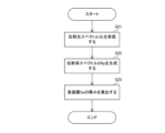
- FIG. 21 is a flowchart showing an example of an operational procedure for a thickness calculation device according to a second embodiment of the present invention to calculate the thickness of a surface layer.
- the thickness calculation device 202 receives from the spectrometer 101 the reflected light spectrum SL from the target sample P of the light irradiated from the surface layer Sa side of the target sample P (step S21).
- the thickness calculation device 202 Based on the reflected light spectrum SL, the thickness calculation device 202 generates a reflectance spectrum SRp in a wavelength range Rr where the round-trip internal transmittance Ia(d) of the surface layer Sa is equal to or greater than the threshold value Th1, and the round-trip internal transmittance Iab(d) of the layer consisting of the surface layer Sa and the adjacent lower layer Sb is equal to or less than the threshold value Th1 (step S22).
- the thickness calculation device 202 calculates the thickness of the surface layer Sa based on the reflectance spectrum SRp (step S23).
Landscapes
- Physics & Mathematics (AREA)
- General Physics & Mathematics (AREA)
- Spectroscopy & Molecular Physics (AREA)
- Length Measuring Devices By Optical Means (AREA)
- Analytical Chemistry (AREA)
- Chemical & Material Sciences (AREA)
- Life Sciences & Earth Sciences (AREA)
- Biochemistry (AREA)
- General Health & Medical Sciences (AREA)
- Immunology (AREA)
- Pathology (AREA)
- Health & Medical Sciences (AREA)
- Mathematical Physics (AREA)
Abstract
Priority Applications (4)
| Application Number | Priority Date | Filing Date | Title |
|---|---|---|---|
| CN202380101333.0A CN121666521A (zh) | 2023-08-22 | 2023-08-22 | 分光器、厚度测定系统、厚度计算装置、分光器的制造方法及厚度计算方法 |
| PCT/JP2023/030153 WO2025041264A1 (fr) | 2023-08-22 | 2023-08-22 | Spectromètre, système de mesure d'épaisseur, dispositif de calcul d'épaisseur, procédé de production de spectromètre et procédé de calcul d'épaisseur |
| KR1020267004867A KR20260038934A (ko) | 2023-08-22 | 2023-08-22 | 분광기, 두께 측정 시스템, 두께 산출 장치, 분광기의 제조 방법 및 두께 산출 방법 |
| TW113116988A TW202510132A (zh) | 2023-08-22 | 2024-05-08 | 分光器、厚度測定系統、厚度算出裝置、分光器之製造方法及厚度算出方法 |
Applications Claiming Priority (1)
| Application Number | Priority Date | Filing Date | Title |
|---|---|---|---|
| PCT/JP2023/030153 WO2025041264A1 (fr) | 2023-08-22 | 2023-08-22 | Spectromètre, système de mesure d'épaisseur, dispositif de calcul d'épaisseur, procédé de production de spectromètre et procédé de calcul d'épaisseur |
Publications (1)
| Publication Number | Publication Date |
|---|---|
| WO2025041264A1 true WO2025041264A1 (fr) | 2025-02-27 |
Family
ID=94731527
Family Applications (1)
| Application Number | Title | Priority Date | Filing Date |
|---|---|---|---|
| PCT/JP2023/030153 Pending WO2025041264A1 (fr) | 2023-08-22 | 2023-08-22 | Spectromètre, système de mesure d'épaisseur, dispositif de calcul d'épaisseur, procédé de production de spectromètre et procédé de calcul d'épaisseur |
Country Status (4)
| Country | Link |
|---|---|
| KR (1) | KR20260038934A (fr) |
| CN (1) | CN121666521A (fr) |
| TW (1) | TW202510132A (fr) |
| WO (1) | WO2025041264A1 (fr) |
Citations (4)
| Publication number | Priority date | Publication date | Assignee | Title |
|---|---|---|---|---|
| JPH0755435A (ja) * | 1993-08-20 | 1995-03-03 | Dainippon Screen Mfg Co Ltd | 多層膜試料の膜厚測定方法 |
| JP2008286583A (ja) * | 2007-05-16 | 2008-11-27 | Otsuka Denshi Co Ltd | 光学特性測定装置および測定方法 |
| JP2009139360A (ja) * | 2007-06-05 | 2009-06-25 | Ricoh Co Ltd | 膜厚測定方法および膜厚測定装置および膜厚測定装置を有する画像形成装置、感光体および感光体の製造方法 |
| JP2014055780A (ja) * | 2012-09-11 | 2014-03-27 | Otsuka Denshi Co Ltd | 膜厚測定方法及び膜厚測定装置 |
-
2023
- 2023-08-22 WO PCT/JP2023/030153 patent/WO2025041264A1/fr active Pending
- 2023-08-22 CN CN202380101333.0A patent/CN121666521A/zh active Pending
- 2023-08-22 KR KR1020267004867A patent/KR20260038934A/ko active Pending
-
2024
- 2024-05-08 TW TW113116988A patent/TW202510132A/zh unknown
Patent Citations (4)
| Publication number | Priority date | Publication date | Assignee | Title |
|---|---|---|---|---|
| JPH0755435A (ja) * | 1993-08-20 | 1995-03-03 | Dainippon Screen Mfg Co Ltd | 多層膜試料の膜厚測定方法 |
| JP2008286583A (ja) * | 2007-05-16 | 2008-11-27 | Otsuka Denshi Co Ltd | 光学特性測定装置および測定方法 |
| JP2009139360A (ja) * | 2007-06-05 | 2009-06-25 | Ricoh Co Ltd | 膜厚測定方法および膜厚測定装置および膜厚測定装置を有する画像形成装置、感光体および感光体の製造方法 |
| JP2014055780A (ja) * | 2012-09-11 | 2014-03-27 | Otsuka Denshi Co Ltd | 膜厚測定方法及び膜厚測定装置 |
Also Published As
| Publication number | Publication date |
|---|---|
| TW202510132A (zh) | 2025-03-01 |
| CN121666521A (zh) | 2026-03-13 |
| KR20260038934A (ko) | 2026-03-19 |
Similar Documents
| Publication | Publication Date | Title |
|---|---|---|
| US7719675B2 (en) | Method for optical characterization and evaluation of optically variable devices and media | |
| KR101159380B1 (ko) | 파면 조정 및 향상된 3?d 측정을 위한 방법 및 장치 | |
| US10365163B2 (en) | Optical critical dimension metrology | |
| TWI793321B (zh) | 光學量測裝置及光學量測方法 | |
| US20190101373A1 (en) | Apparatus for measuring thickness and surface profile of multilayered film structure using imaging spectral optical system and measuring method | |
| CN112384750B (zh) | 双干涉测量样本测厚仪 | |
| KR20130018553A (ko) | 막 두께 측정 장치 | |
| JP2005530144A (ja) | 単一構造の光学測定法 | |
| JP2010019636A (ja) | 多層構造計測方法および多層構造計測装置 | |
| JP2007533977A5 (fr) | ||
| JP2007532931A (ja) | 薄膜及び限界寸法測定のためのビーム・プロファイル式複合反射率システム及び方法 | |
| WO2011083544A1 (fr) | Appareil de mesure de l'épaisseur d'un film à l'aide d'interférences, et procédé de mesure de l'épaisseur d'un film à l'aide d'interférences | |
| TW200532164A (en) | Film thickness measuring method and apparatus | |
| US11248900B2 (en) | Method and assembly for chromatic confocal spectral interferometry or spectral domain oct | |
| TWI458960B (zh) | 白光干涉量測裝置及其干涉量測方法 | |
| KR101547459B1 (ko) | 위상 축소 이미징 시스템 및 이를 이용한 이미징 방법 | |
| WO2025041264A1 (fr) | Spectromètre, système de mesure d'épaisseur, dispositif de calcul d'épaisseur, procédé de production de spectromètre et procédé de calcul d'épaisseur | |
| KR101722815B1 (ko) | 시료의 표면 측정 방법 및 장치 | |
| KR100945314B1 (ko) | 형상 측정 장치, 노광 장치 및 컴퓨터 | |
| JP3634327B2 (ja) | 光波長分散空間干渉断層画像化装置 | |
| TWI913560B (zh) | 影像擷取裝置、測量裝置及物品製造方法 | |
| KR20250111288A (ko) | Tsv를 위한 간섭 분광법 | |
| JP2011089972A (ja) | 光学検査システム、光学検査装置 | |
| CN118347968A (zh) | 体全息光栅平均折射率的测量方法 | |
| Korolkov et al. | Application of fiber spectrometers for etch depth measurement of binary computer-generated holograms |
Legal Events
| Date | Code | Title | Description |
|---|---|---|---|
| 121 | Ep: the epo has been informed by wipo that ep was designated in this application |
Ref document number: 23949725 Country of ref document: EP Kind code of ref document: A1 |
|
| ENP | Entry into the national phase |
Ref document number: 2025541216 Country of ref document: JP Kind code of ref document: A |
|
| WWE | Wipo information: entry into national phase |
Ref document number: 2025541216 Country of ref document: JP |
|
| ENP | Entry into the national phase |
Ref document number: 1020267004867 Country of ref document: KR Free format text: ST27 STATUS EVENT CODE: A-0-1-A10-A15-NAP-PA0105 (AS PROVIDED BY THE NATIONAL OFFICE) |
|
| WWE | Wipo information: entry into national phase |
Ref document number: 1020267004867 Country of ref document: KR |
|
| WWP | Wipo information: published in national office |
Ref document number: 1020267004867 Country of ref document: KR |
|
| NENP | Non-entry into the national phase |
Ref country code: DE |