WO2025041264A1 - Spectrometer, thickness measurement system, thickness calculation device, method for producing spectrometer, and method for calculating thickness - Google Patents
Spectrometer, thickness measurement system, thickness calculation device, method for producing spectrometer, and method for calculating thickness Download PDFInfo
- Publication number
- WO2025041264A1 WO2025041264A1 PCT/JP2023/030153 JP2023030153W WO2025041264A1 WO 2025041264 A1 WO2025041264 A1 WO 2025041264A1 JP 2023030153 W JP2023030153 W JP 2023030153W WO 2025041264 A1 WO2025041264 A1 WO 2025041264A1
- Authority
- WO
- WIPO (PCT)
- Prior art keywords
- surface layer
- thickness
- layer
- round
- internal transmittance
- Prior art date
- Legal status (The legal status is an assumption and is not a legal conclusion. Google has not performed a legal analysis and makes no representation as to the accuracy of the status listed.)
- Pending
Links
Images


Classifications
-
- G—PHYSICS
- G01—MEASURING; TESTING
- G01B—MEASURING LENGTH, THICKNESS OR SIMILAR LINEAR DIMENSIONS; MEASURING ANGLES; MEASURING AREAS; MEASURING IRREGULARITIES OF SURFACES OR CONTOURS
- G01B11/00—Measuring arrangements characterised by the use of optical techniques
- G01B11/02—Measuring arrangements characterised by the use of optical techniques for measuring length, width or thickness
- G01B11/06—Measuring arrangements characterised by the use of optical techniques for measuring length, width or thickness for measuring thickness ; e.g. of sheet material
Definitions
- the present invention relates to a spectrometer, a thickness measurement system, a thickness calculation device, a method for manufacturing a spectrometer, and a method for calculating thickness.
- Patent Document 1 JP Patent Publication 2014-55780A discloses a film thickness measurement method as follows. That is, the film thickness measurement method uses a sample including a reference film having a first wavelength region and a second wavelength region with a difference in light transmittance, the first wavelength region having a lower light transmittance than the second wavelength region, one or more measurement target films formed on one side of the reference film, and one or more measurement target films formed on the other side of the reference film, and measures the thickness of each of the measurement target films, and includes an irradiation step of irradiating the sample with light from the one side, a measurement step of measuring the reflectance spectrum of the light by the sample in part or all of the first wavelength region and part or all of the second wavelength region, a first calculation step of calculating the thickness of each of the measurement target films formed on the one side based on the reflectance spectrum in the first wavelength region, and a second calculation step of calculating the thickness of each of the films formed on the other side based on the thickness of each of the measurement
- Patent Document 2 JP 2008-286583 A discloses an optical property measuring device equipped with a Cassegrain-type reflective objective lens.
- the reflective objective lens includes a convex reflector and a concave reflector arranged so that the central axis coincides with the optical axis.
- the optical property measuring device described in Patent Document 2 the measurement reflected light generated by reflection from the surface of the object to be measured passes through a pinhole and enters the spectroscopic measurement unit, while the back-reflected light generated by reflection from the back surface of the object to be measured cannot pass through the pinhole. Therefore, the optical property measuring device described in Patent Document 2 can avoid the effects of back-reflected light, i.e., stray light.
- the present invention has been made to solve the above-mentioned problems, and its purpose is to provide a spectrometer, a thickness measurement system, a thickness calculation device, a method for manufacturing a spectrometer, and a thickness calculation method that are capable of more accurately measuring the thickness of the surface layer of a target sample with a multi-layer structure.
- a spectrometer used to measure the thickness of a surface layer of a target sample having a multilayer structure in which a surface layer and an underlayer are stacked, and includes a light receiving section that receives light reflected from the target sample of light irradiated from the surface layer side of the target sample, and a spectroscopic section that generates a reflected light spectrum by dispersing the reflected light, and the spectroscopic section generates the reflected light spectrum in a spectral wavelength range in which the round-trip internal transmittance of the surface layer is equal to or greater than a predetermined lower limit, and the round-trip internal transmittance of the layer consisting of the surface layer and the underlayer is equal to or less than a predetermined upper limit.
- a reflected light spectrum can be generated that includes the components of reflected light at the light-irradiated surface of the surface layer and the components of reflected light at the interface between the surface layer and the lower layer, while reducing the components of reflected light at the interface on the opposite side of the interface in the lower layer.
- the thickness of the surface layer can be calculated more accurately based on the reflectance spectrum, which is the interference waveform of the surface layer generated using the reflected light spectrum. Therefore, the thickness of the surface layer in a target sample with a multilayer structure can be measured more accurately.
- the "round-trip internal transmittance I(d)" corresponds to the component of light incident on a layer of thickness d that is reflected at the interface opposite to the incident surface, i.e., the back surface, and returns to the incident surface, and is the attenuation due to material absorption in the round-trip process in the layer expressed as transmittance.
- the spectroscopic unit may generate the reflected light spectrum in the spectroscopic wavelength range in which, within the thickness range of the surface layer, the round-trip internal transmittance of the surface layer is equal to or greater than a predetermined threshold, and the round-trip internal transmittance of the combined layer of the surface layer and the lower layer is equal to or less than the threshold.
- a reflected light spectrum that is more effective in thickness measurement, taking into account detection limits based on noise, dynamic range, etc.
- This configuration allows for more accurate measurement of the thickness of the silicon layer that constitutes the main surface of the multi-layer structure.
- a thickness measurement system includes a spectrometer as described above in (1) to (3), and a macro-optical system that irradiates the surface layer side of the target sample with light from a light source and guides the reflected light from the target sample to the spectrometer.
- This configuration allows the thickness of the surface layer to be measured more quickly than a microspectrophotometer such as the optical property measuring device described in Patent Document 2.
- a thickness calculation device used to measure the thickness of a surface layer of a target sample having a multilayer structure in which a surface layer and a lower layer are stacked, and includes an acquisition unit that acquires a reflected light spectrum of light reflected from the target sample by light irradiated from the surface layer side of the target sample, a generation unit that generates a reflectance spectrum of the target sample based on the reflected light spectrum acquired by the acquisition unit, and a calculation unit that calculates the thickness of the surface layer based on the reflectance spectrum generated by the generation unit, and the generation unit generates the reflectance spectrum in a wavelength range in which the round-trip internal transmittance of the surface layer is equal to or greater than a predetermined lower limit and the round-trip internal transmittance of the layer consisting of the surface layer and the lower layer is equal to or less than a predetermined upper limit.
- a reflectance spectrum is generated in a wavelength range where the round-trip internal transmittance of the surface layer is equal to or greater than a predetermined lower limit and the round-trip internal transmittance of the combined surface layer and lower layer is equal to or less than an upper limit based on the reflected light spectrum of the reflected light of the target sample, and the thickness is calculated based on the reflectance spectrum.
- This makes it possible to generate a reflectance spectrum that includes components of reflected light at the light-irradiated surface of the surface layer and components of reflected light at the interface between the surface layer and the lower layer, while reducing components of reflected light at the interface of the lower layer on the opposite side to the interface. Therefore, the thickness of the surface layer can be calculated more accurately using the generated reflectance spectrum. Therefore, the thickness of the surface layer of a target sample with a multilayer structure can be measured more accurately.
- the generating unit may generate the reflectance spectrum in the wavelength range in which, within the thickness range of the surface layer, the round-trip internal transmittance of the surface layer is equal to or greater than a predetermined threshold, and the round-trip internal transmittance of the layer consisting of the surface layer and the lower layer is equal to or less than the threshold.
- a manufacturing method of a spectrometer is a manufacturing method of a spectrometer used for measuring the thickness of a surface layer of a target sample having a multilayer structure in which a surface layer and a lower layer are stacked, and includes the steps of acquiring first correspondence information indicating the correspondence relationship between a wavelength and a round-trip internal transmittance of the surface layer, acquiring second correspondence information indicating the correspondence relationship between a wavelength and a round-trip internal transmittance of a layer formed by combining the surface layer and the lower layer, and setting a spectroscopic wavelength range of the spectrometer that splits light reflected from the target sample of light irradiated from the surface layer side of the target sample based on the acquired first correspondence information and second correspondence information, and in the step of setting the spectroscopic wavelength range, the spectroscopic wavelength range is set so that the round-trip internal transmittance of the surface layer is equal to or greater than a predetermined
- the thickness of the surface layer can be calculated more accurately using the reflectance spectrum, which is the interference waveform of the surface layer generated using the reflected light spectrum. Therefore, the thickness of the surface layer in a target sample having a multi
- the method of manufacturing the spectrometer may further include a step of acquiring a thickness range of the surface layer, and in the step of setting the spectroscopic wavelength range, the spectroscopic wavelength range may be set within a wavelength range between a first wavelength, which is the wavelength at which the round-trip internal transmittance of the surface layer reaches a predetermined threshold value when the thickness of the surface layer is the maximum value of the thickness range, and a second wavelength, which is the wavelength at which the round-trip internal transmittance of the combined layer of the surface layer and the underlayer reaches the threshold value when the thickness of the surface layer is the minimum value of the thickness range.
- a first wavelength which is the wavelength at which the round-trip internal transmittance of the surface layer reaches a predetermined threshold value when the thickness of the surface layer is the maximum value of the thickness range
- a second wavelength which is the wavelength at which the round-trip internal transmittance of the combined layer of the surface layer and the underlayer reaches the threshold value when the thickness of the surface layer is the minimum value of the
- a spectrometer capable of generating a reflected light spectrum that is more effective in thickness measurement, taking into account detection limits based on noise, dynamic range, etc.
- the specifications of a spectrometer capable of generating a reflected light spectrum in which the level of reflected light reflected at the interface between the surface layer and the lower layer is equal to or higher than the noise level, and the level of reflected light reflected at the interface between the lower layer and another lower layer is equal to or lower than the noise level.
- a thickness calculation method is a thickness calculation method in a thickness calculation device used to measure the thickness of a surface layer of a target sample having a multilayer structure in which a surface layer and an underlayer are stacked, and includes the steps of acquiring a reflected light spectrum of light reflected from the target sample, the light being irradiated from the surface layer side of the target sample, generating a reflectance spectrum of the target sample based on the acquired reflected light spectrum, and calculating the thickness of the surface layer based on the generated reflectance spectrum, and in the step of generating the reflectance spectrum, the reflectance spectrum is generated in a wavelength range in which the round-trip internal transmittance of the surface layer is equal to or greater than a predetermined lower limit, and the round-trip internal transmittance of the combined layer of the surface layer and the underlayer is equal to or less than a predetermined upper limit.
- the thickness of the surface layer can be calculated more accurately using the generated reflectance spectrum. Therefore, the thickness of the surface layer of a target sample with a multilayer structure can be measured more accurately.
- the present invention makes it possible to more accurately measure the thickness of the surface layer of a multi-layered target sample.
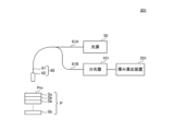
- FIG. 1 is a diagram showing the configuration of a thickness measurement system according to a first embodiment of the present invention.
- FIG. 2 is a diagram showing a configuration of a thickness calculation device according to the first embodiment of the present invention.
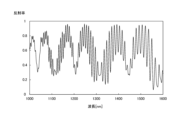
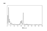
- FIG. 3 is a diagram showing a simulation result of thickness measurement of a target sample by a thickness measurement system according to a comparative example.
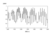
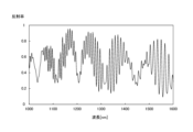
- FIG. 4 is a diagram showing a simulation result of thickness measurement of a target sample by a thickness measurement system according to a comparative example.
- FIG. 5 is a diagram showing a simulation result of thickness measurement of a target sample by a thickness measurement system according to a comparative example.
- FIG. 6 is a diagram showing a simulation result of thickness measurement of a target sample by a thickness measurement system according to a comparative example.
- FIG. 1 is a diagram showing the configuration of a thickness measurement system according to a first embodiment of the present invention.
- FIG. 2 is a diagram showing a configuration of a thickness calculation device according to the first embodiment of
- FIG. 7 is a diagram showing a simulation result of thickness measurement of a target sample by a thickness measurement system according to a comparative example.
- FIG. 8 is a diagram showing a simulation result of thickness measurement of a target sample by the thickness measurement system according to the comparative example.
- FIG. 9 is a diagram showing the configuration of a spectrometer according to the first embodiment of the present invention.
- FIG. 10 is a diagram showing the simulation results of the round-trip internal transmittance of the surface layer.
- FIG. 11 is a diagram showing the extinction coefficient of silicon.
- FIG. 12 shows a reflectance spectrum SR generated in the thickness measurement system according to the first embodiment of the present invention.
- FIG. 13 shows a reflectance spectrum SR generated in the thickness measurement system according to the first embodiment of the present invention.
- FIG. 14 shows a reflectance spectrum SR generated in the thickness measurement system according to the first embodiment of the present invention.
- FIG. 15 shows a power spectrum generated in the thickness measurement system according to the first embodiment of the present invention.
- FIG. 16 shows a power spectrum generated in the thickness measurement system according to the first embodiment of the present invention.
- FIG. 17 shows a power spectrum generated in the thickness measurement system according to the first embodiment of the present invention.
- FIG. 18 is a flowchart showing a method for manufacturing a spectroscope in the thickness measurement system according to the first embodiment of the present invention.
- FIG. 19 is a diagram showing a configuration of a thickness measurement system according to the second embodiment of the present invention.
- FIG. 20 is a diagram showing a configuration of a thickness calculation device according to the second embodiment of the present invention.
- FIG. 21 is a flowchart defining an example of an operational procedure when the thickness calculation device according to the second embodiment of the present invention calculates the thickness of a surface layer.
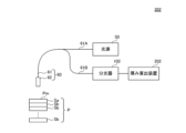
- First Embodiment 1 is a diagram showing a configuration of a thickness measurement system according to a first embodiment of the present invention.
- the thickness measurement system 301 includes a light source 50, a macro optical system 60, a spectroscope 101, and a thickness calculation device 201.
- the thickness measurement system 301 is a spectral interference type measurement system, and is used to measure the thickness of a surface layer Sa in a target sample P having a multilayer structure in which a surface layer Sa and a lower layer Sb are laminated.
- the surface of the surface layer Sa is the main surface Pm of the target sample P.
- the lower limit of the thickness range Rth of the surface layer Sa to be measured is 1 ⁇ m or more, and the upper limit of the thickness range Rth is 20 ⁇ m or less.
- the shape of the target sample P may be a wafer shape, a rectangular shape, or a film shape.
- the target sample P includes a surface layer Sa and multiple lower layers Sb.
- the surface layer Sa is a silicon layer
- the lower layers Sb are silicon layers coated with a silicon oxide thin film.
- the target sample P has a repeating layer structure in which multiple silicon layers coated with a silicon oxide thin film are stacked as the lower layers Sb from the surface layer Sa side.
- the target sample P has a repeating layer structure in which a silicon oxide layer, which is a coating, and a silicon layer are alternately stacked as the lower layers Sb from the surface layer Sa side.
- the target sample P may be configured to include one lower layer Sb.
- the lower layer Sb adjacent to the surface layer Sa i.e., the lower layer Sb directly below the surface layer Sa, is also referred to as the "adjacent lower layer Sb".
- the light source 50 emits light used to measure the thickness of the surface layer Sa.
- the light source 50 emits light including multiple wavelengths.
- the spectrum of the light emitted by the light source 50 is a continuous spectrum.
- the range of wavelengths of the light emitted by the light source 50 includes the spectral wavelength range Rs1 of the spectroscope 101.
- the light source 50 is, for example, a halogen lamp.
- the macro optical system 60 irradiates the surface layer Sa side of the target sample P with light from the light source 50, and guides the reflected light of the irradiated light from the target sample P to the spectrometer 101. More specifically, the macro optical system 60 includes a Y-type optical fiber 61 and a probe 62. The probe 62 is provided at a first end of the Y-type optical fiber 61. The second end of the Y-type optical fiber 61 is bifurcated. The branched portion 61A of the Y-type optical fiber 61 is connected to the light source 50. The branched portion 61B of the Y-type optical fiber 61 is connected to the spectrometer 101.
- the light emitted from the light source 50 is irradiated onto the main surface Pm of the target sample P via the Y-type optical fiber 61 and the probe 62.
- the reflected light from the target sample P of the light irradiated onto the main surface Pm is guided to the spectrometer 101 via the probe 62 and the Y-type optical fiber 61.
- the thickness measurement system 301 may be configured to include an optical system including a lens, a beam splitter, etc., instead of the macro optical system 60.
- the spectrometer 101 generates a reflected light spectrum SL including a spectroscopic wavelength range Rs1 by dispersing the reflected light from the target sample P.
- the spectrometer 101 generates a reflected light spectrum SL in the spectroscopic wavelength range Rs1 by dispersing the reflected light from the target sample P.
- the spectrometer 101 transmits the generated reflected light spectrum SL to the thickness calculation device 201.
- FIG. 2 is a diagram showing the configuration of a thickness calculation device according to a first embodiment of the present invention.
- the thickness calculation device 201 includes a receiving unit 21, a generating unit 22, and a calculating unit 23.
- the receiving unit 21 is an example of an acquisition unit.
- the receiving unit 21, the generating unit 22, and a part or all of the calculating unit 23 are realized, for example, by a processing circuit including one or more processors.
- the receiver 21 receives from the spectrometer 101 the reflected light spectrum SL from the target sample P irradiated with light from the surface layer Sa side, and outputs the received reflected light spectrum SL to the generator 22.
- the generating unit 22 generates a reflectance spectrum SR of the target sample P based on the reflected light spectrum SL received from the receiving unit 21. More specifically, the generating unit 22 generates the reflectance spectrum SR by dividing the reflected light spectrum SL by the irradiated light spectrum of the light irradiated to the target sample P. The generating unit 22 outputs the generated reflectance spectrum SR to the calculating unit 23.
- the calculation unit 23 calculates the thickness of the surface layer Sa based on the reflectance spectrum SR generated by the generation unit 22. For example, the calculation unit 23 calculates the thickness of the surface layer Sa by analyzing the reflectance spectrum SR according to the FFT (Fast Fourier Transform) method. More specifically, the calculation unit 23 generates a power spectrum of the reflectance spectrum SR by performing FFT processing on the reflectance spectrum SR. Then, the calculation unit 23 identifies a thickness that meets the given selection conditions from the generated power spectrum as the thickness of the surface layer Sa.
- FFT Fast Fourier Transform
- a reflectance spectrum SR in a wavelength range in which the internal transmittance of the film is high by dispersing light reflected from the film when light is irradiated from the outside onto the main surface of the film, and to calculate the thickness based on the reflectance spectrum SR.
- a conventional thickness measurement system when measuring the thickness of a silicon film, for example, a conventional thickness measurement system generates a reflected light spectrum SL using a spectrometer with a spectral wavelength range of 1000 nm or more, where the extinction coefficient of the silicon film is close to zero, and calculates the thickness of the silicon layer based on the generated reflected light spectrum SL.
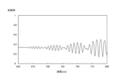
- Figures 3 to 8 show the simulation results of thickness measurement of a target sample using a thickness measurement system according to a comparative example.
- Figures 3 to 5 show reflectance spectra SR generated in a comparative thickness measurement system equipped with a spectrometer having a spectral wavelength range of 1000 nm or more and sufficient wavelength resolution.
- the horizontal axis is wavelength [nm] and the vertical axis is reflectance.
- Figure 3 shows the reflectance spectrum SR of a target sample P1 that includes a 1 ⁇ m silicon layer as a surface layer Sa and includes six alternating layers of 5 ⁇ m silicon oxide layers and 21 ⁇ m silicon layers from the surface layer Sa side as lower layers Sb.
- Figure 4 shows the reflectance spectrum SR of a target sample P2 that includes a 10 ⁇ m silicon layer as a surface layer Sa compared to the target sample P1.
- Figure 5 shows the reflectance spectrum SR of a target sample P3 that includes a 20 ⁇ m silicon layer as a surface layer Sa compared to the target sample P1.
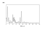
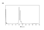
- FIGS. 6 to 8 show power spectra generated in a thickness measurement system according to a comparative example.
- the horizontal axis represents thickness [ ⁇ m] and the vertical axis represents intensity.
- FIG. 6 to FIG. 8 show the power spectra of the reflectance spectrum SR shown in FIG. 3 to FIG. 5, respectively.
- the thickness measurement system according to the comparative example cannot accurately measure the thickness of the surface layer Sa of the target sample P1. More specifically, in the power spectra of the target samples P1, P2, and P3 generated by the thickness measurement system according to the comparative example, the thickness corresponding to the maximum intensity is approximately 2 ⁇ m. Therefore, the measurement result of the thickness of the surface layer Sa by the thickness measurement system according to the comparative example is approximately 2 ⁇ m, even though the actual thickness of the surface layer Sa is 1 ⁇ m, 10 ⁇ m, or 20 ⁇ m.
- the thickness of the target samples P1, P2, and P3 having a multilayer structure is measured using the thickness measurement system according to the comparative example, it is difficult to measure the thickness of the surface layer Sa. Furthermore, even if the reflectance spectrum SR could be separated into layers, it is difficult to identify which layer the thickness calculated based on the reflectance spectrum SR indicates.
- Patent Document 1 requires that the substrate film has a transmittance in a specified wavelength band that is smaller than that of the coating film, and measurements cannot be made if the coating film has a smaller transmittance than the substrate film. Furthermore, with the technology described in Patent Document 1, when multiple layers are stacked on one side of the substrate film, it is not possible to measure the thickness of the surface layer of the multiple layers.
- Patent Document 2 also describes a technique for suppressing light from the back surface of the object being measured from appearing as stray light by using a Cassegrain-type reflective objective lens.
- the technique described in Patent Document 2 has significant design constraints.
- the thickness measurement system 301 solves the above problems by adopting the following configuration.
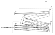
- Fig. 9 is a diagram showing the configuration of a spectrometer according to a first embodiment of the present invention.
- spectrometer 101 includes slit 11 and spectroscopic section 12.
- Spectroscopic section 12 includes diffraction grating 12A, detection section 12B, collimator mirror 12C, and focus mirror 12D.
- Slit 11 is an example of a light receiving section.
- the slit 11 receives the reflected light from the target sample P of the light irradiated from the surface layer Sa side of the target sample P. More specifically, the slit 11 receives the reflected light from the target sample P via the branching portion 61B of the Y-shaped optical fiber 61. The reflected light from the target sample P that enters the inside of the spectroscope 101 from the slit 11 is collimated by the collimating mirror 12C.
- the spectroscopic unit 12 generates a reflected light spectrum SL by dispersing the reflected light from the target sample P.
- the light that has been collimated by the collimating mirror 12C is guided to the diffraction grating 12A.
- the diffraction grating 12A separates the incident light into different diffraction angles for each wavelength.
- the light split into different angles for each wavelength by the diffraction grating 12A is focused by the focus mirror 12D at different positions for each wavelength in the detection unit 12B.
- the detection unit 12B is a linear image sensor composed of multiple detection elements arranged in a line.
- detection elements are, for example, a CCD (Charge Coupled Device) image sensor or a CMOS (Complementary Metal Oxide Semiconductor) image sensor.
- CCD Charge Coupled Device
- CMOS Complementary Metal Oxide Semiconductor
- the detection unit 12B generates a reflected light spectrum SL that indicates the relationship between the wavelength and intensity of the light received on the light receiving surface of each detection element, and transmits the generated reflected light spectrum SL to the thickness calculation device 201.
- the wavelength resolution of the reflected light spectrum SL generated by the spectroscopic section 12 satisfies the following expressions (1) and (2).
- R1 is the optical resolution.
- R2 is the pixel resolution.
- ⁇ 1 is the wavelength corresponding to the maximum intensity value M1 in the reflected light spectrum SL.
- ⁇ 2 is the wavelength corresponding to the maximum intensity value M2 in the reflected light spectrum SL.
- Maximum value M2 is a maximum value that is greater than and adjacent to maximum value M1.
- the spectroscopic unit 12 generates a reflected light spectrum SL in a spectroscopic wavelength range Rs1 in which the round-trip internal transmittance Ia(d), which is the round-trip internal transmittance I(d) of the surface layer Sa, is equal to or greater than a predetermined lower limit, and the round-trip internal transmittance Iab(d), which is the round-trip internal transmittance I(d) of the layer consisting of the surface layer Sa and the adjacent lower layer Sb, is equal to or less than a predetermined upper limit.
- the round-trip internal transmittance Iab(d) corresponds to the round-trip internal transmittance of a silicon layer having a thickness equal to the sum of the thickness of the surface layer Sa and the thickness of the silicon layer in the adjacent lower layer Sb.
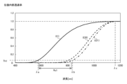
- FIG. 10 is a diagram showing the simulation results of the round-trip internal transmittance.
- the horizontal axis is the wavelength [nm]
- the vertical axis is the round-trip internal transmittance.
- the solid line in FIG. 10 indicates the round-trip internal transmittance I(1), which is the round-trip internal transmittance I(d) of a 1 ⁇ m silicon layer.
- the dashed line in FIG. 10 indicates the round-trip internal transmittance I(20), which is the round-trip internal transmittance I(d) of a 20 ⁇ m silicon layer.
- the dashed line in FIG. 10 indicates the round-trip internal transmittance I(21), which is the round-trip internal transmittance I(d) of a 21 ⁇ m silicon layer.
- the round-trip internal transmittance I(1) is the round-trip internal transmittance of a 1 ⁇ m silicon layer, so it corresponds to the internal transmittance of a 2 ⁇ m silicon layer.
- the round-trip internal transmittance I(20) is the round-trip internal transmittance of a 20 ⁇ m silicon layer, so it corresponds to the internal transmittance of a 40 ⁇ m silicon layer.
- the round-trip internal transmittance I(21) is the round-trip internal transmittance of a 21 ⁇ m silicon layer, which corresponds to the internal transmittance of a 42 ⁇ m silicon layer.
- the spectroscopic unit 12 generates a reflected light spectrum SL in a spectroscopic wavelength range Rs1 where the round-trip internal transmittance Ia(d) of the surface layer Sa is equal to or greater than a predetermined threshold Th1, and the round-trip internal transmittance Iab(d) of the layer consisting of the surface layer Sa and the adjacent lower layer Sb is equal to or less than the threshold Th1, in the thickness range Rth.
- the threshold Th1 is an example of a lower limit and an example of an upper limit.
- the spectral wavelength range Rs1 is set within the wavelength range between the wavelength ⁇ a when the round-trip internal transmittance Ia(1) of the surface layer Sa becomes the threshold value Th1 and the wavelength ⁇ b when the round-trip internal transmittance Iab(21) of the layer including the surface layer Sa and the adjacent lower layer Sb becomes the threshold value Th1.
- the wavelength ⁇ a is an example of the first wavelength.
- the wavelength ⁇ b is an example of the second wavelength.
- the threshold value Th1 is a value less than 1.
- the threshold value Th1 is, for example, 0.001.
- the spectral wavelength range Rs1 may be set within the wavelength range between the wavelength ⁇ a when the round-trip internal transmittance Ia(1) becomes the threshold value Th1 and the wavelength ⁇ b when the round-trip internal transmittance Iab(21) becomes the threshold value Th2 different from the threshold value Th1.
- the spectroscopic unit 12 generates a reflected light spectrum SL in a spectroscopic wavelength range Rs1 in which the round-trip internal transmittance Ia(d) of the surface layer Sa is equal to or greater than the noise level in the thickness calculation device 201, and the round-trip internal transmittance Iab(d) of the surface layer Sa and the adjacent lower layer Sb combined is equal to or less than the noise level in the thickness calculation device 201, in the thickness range Rth.
- the spectroscopic unit 12 generates a reflected light spectrum SL in a spectroscopic wavelength range Rs1 in which the level of the reflected light that passes through the surface layer Sa and is reflected at the interface between the surface layer Sa and the adjacent lower layer Sb is equal to or greater than the noise level in the thickness calculation device 201, and the level of the reflected light that passes through the surface layer Sa and the adjacent lower layer Sb and is reflected at the interface between the adjacent lower layer Sb and another lower layer Sb is equal to or less than the noise level in the thickness calculation device 201, in the thickness range Rth.
- the spectral wavelength range Rs1 is a wavelength range in which the round-trip internal transmittance Ia(d) is equal to or greater than the noise level in the thickness calculation device 201, and in which a sufficient number of interference waves can be obtained for FFT analysis, and in which the combined round-trip internal transmittance Iab(d) of the surface layer Sa and the adjacent lower layer Sb is equal to or less than the noise level in the thickness calculation device 201.
- the spectral wavelength range Rs1 is a wavelength range in which the absolute value of the change in the round-trip internal transmittance of the surface layer Sa with respect to wavelength is equal to or greater than a predetermined value.
- the spectral wavelength range Rs1 of the spectroscopic section 12 is a wavelength range that does not include wavelengths equal to or greater than the wavelength ⁇ c, where there is almost no change in the round-trip internal transmittance Ia(d) of the surface layer Sa, and does not include the ultraviolet range in which there is almost no transmission.
- the spectral wavelength range Rs1 of the spectroscopic section 12 is a wavelength range that is smaller than the wavelength ⁇ c.
- the spectral wavelength range Rs1 includes at least a portion of the visible light region.
- the spectroscopic wavelength range Rs1 of the spectroscopic unit 12 is a wavelength range in which the absolute value of the amount of change in the extinction coefficient of the material that constitutes the surface layer Sa with respect to wavelength is equal to or greater than a predetermined value.
- the spectroscopic wavelength range Rs1 of the spectroscopic unit 12 is a wavelength range that is shorter than the wavelength at which the decrease in the extinction coefficient of silicon, which is the material that constitutes the surface layer Sa, converges, and does not include a range in which the extinction coefficient is extremely large.
- FIG. 11 is a diagram showing the extinction coefficient of silicon.
- the horizontal axis is wavelength [nm] and the vertical axis is extinction coefficient.
- the designer of the spectrometer 101 performs the following process to determine the specifications. That is, the designer of the spectrometer 101 obtains the extinction coefficient of silicon, which is the material that constitutes the surface layer Sa and the adjacent lower layer Sb.
- the designer of the spectrometer 101 also obtains the thickness range Rth of the surface layer Sa to be measured.
- the thickness range Rth is the range of thicknesses that can be measured by the thickness measurement system 301.
- the designer of the spectrometer 101 may set the thickness range Rth according to the target sample P, or may set the thickness range Rth according to the needs of the user of the thickness measurement system 301. For example, the designer of the spectrometer 101 also obtains the thickness range of the adjacent lower layer Sb.
- the designer of the spectroscope 101 creates correspondence information X1 indicating the correspondence relationship between the wavelength of light incident on the surface layer Sa and the round-trip internal transmittance Ia(d) of the surface layer Sa based on the acquired extinction coefficient and thickness range Rth.
- the designer of the spectroscope 101 also creates correspondence information X2 indicating the correspondence relationship between the wavelength of light incident on the surface layer Sa and the round-trip internal transmittance Iab(d) of the layer including the surface layer Sa and the adjacent lower layer Sb based on the acquired extinction coefficient, thickness range Rth, and thickness of the adjacent lower layer Sb.
- the designer of the spectroscope 101 calculates the round-trip internal transmittance Ia(d) at the lower limit of the thickness range Rth and the round-trip internal transmittance Ia(d) at the upper limit of the thickness range Rth according to the following formula (3).
- d is the thickness of the surface layer Sa
- ⁇ is the absorption coefficient, which is expressed by the following formula (4).
- ⁇ is the wavelength of light irradiated from the light source 50 to the surface layer Sa.
- k( ⁇ ) is the extinction coefficient of light with wavelength ⁇ .
- the designer of the spectrometer 101 sets the spectral wavelength range Rs1, based on the correspondence information X1 and X2, in which the round-trip internal transmittance I(d) of the surface layer Sa is equal to or greater than the threshold value Th1, and the round-trip internal transmittance Iab(d) of the layer consisting of the surface layer Sa and the adjacent lower layer Sb is equal to or less than the threshold value Th1.
- the designer of the spectrometer 101 sets the spectral wavelength range Rs1 within the wavelength range between the wavelength ⁇ a when the round-trip internal transmittance Ia(1) becomes the threshold value Th1, and the wavelength ⁇ b when the round-trip internal transmittance Iab(21) becomes the threshold value Th1, as described above.
- the designer of the spectrometer 101 sets a spectral wavelength range Rs1 based on the correspondence information X1 and X2, in which the round-trip internal transmittance Ia(d) of the surface layer Sa is equal to or greater than the noise level in the thickness calculation device 201, the round-trip internal transmittance Iab(d) of the surface layer Sa and the adjacent lower layer Sb is equal to or less than the noise level in the thickness calculation device 201, and a sufficient number of interference wave numbers of the surface layer Sa are obtained for FFT analysis.
- the spectral wavelength range Rs1 is set so that the round-trip internal transmittance Iab(d) of the surface layer Sa and the adjacent lower layer Sb combined is equal to or less than the noise level in the thickness calculation device 201, and only an interference waveform of a level that does not affect the power spectrum of the FFT analysis of the interference waveform obtained from the surface layer Sa is obtained.
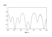
- FIGS. 12 to 14 show reflectance spectra SR generated in a thickness measurement system according to a first embodiment of the present invention.
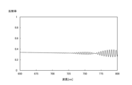
- FIGS. 12 to 14 show reflectance spectra SR generated in a thickness measurement system 301 including a spectrometer 101 having a spectroscopic wavelength range Rs1 of 650 nm or more and 800 nm or less, which is set based on the thickness range Rth of the surface layer Sa.
- the horizontal axis is wavelength [nm]
- the vertical axis is reflectance.
- FIGS. 12 to 14 show reflectance spectra SR of the above-mentioned target samples P1, P2, and P3, respectively.
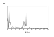
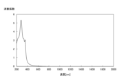
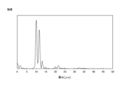
- FIGS. 15 to 17 show power spectra generated in a thickness measurement system according to a first embodiment of the present invention.
- the horizontal axis represents thickness [ ⁇ m] and the vertical axis represents intensity.
- FIG. 15 to FIG. 17 show the power spectra of the reflectance spectrum SR shown in FIG. 12 to FIG. 14, respectively.
- the thickness measurement system 301 can accurately measure the thickness of the surface layer Sa of the target sample P1.
- the thickness corresponding to the maximum intensity is approximately 1 ⁇ m. Therefore, the measurement result of the thickness of the surface layer Sa by the thickness measurement system 301 is approximately equal to the actual thickness of the surface layer Sa.
- the thickness corresponding to the maximum intensity is approximately 10 ⁇ m. Therefore, the measurement result of the thickness of the surface layer Sa by the thickness measurement system 301 is approximately equal to the actual thickness of the surface layer Sa.
- the thickness corresponding to the maximum intensity is approximately 20 ⁇ m. Therefore, the measurement result of the thickness of the surface layer Sa by the thickness measurement system 301 is approximately equal to the actual thickness of the surface layer Sa.
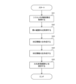
- FIG. 18 is a flowchart showing a method for manufacturing a spectrometer in a thickness measurement system according to a first embodiment of the present invention.
- the designer of the spectrometer 101 performs the following process to determine the specifications.
- the designer of the spectrometer 101 obtains the extinction coefficient of silicon, which is the material that constitutes the surface layer Sa and the adjacent lower layer Sb (step S11).
- the designer of the spectrometer 101 obtains the design values for the thickness range Rth of the surface layer Sa to be measured, and the thickness of the adjacent lower layer Sb (step S12).
- correspondence information X1 that indicates the correspondence between the wavelength of light incident on the surface layer Sa and the round-trip internal transmittance Ia(d) of the surface layer Sa based on the extinction coefficient and the thickness range Rth.
- the correspondence information X1 is information that indicates the wavelength range in which a sufficient number of interference wavenumbers of the surface layer Sa can be obtained for FFT analysis, as well as the spectrometer resolution.
- the designer of the spectrometer 101 calculates the round-trip internal transmittance Ia(1) of the surface layer Sa at the lower limit of the thickness range Rth, and the round-trip internal transmittance Ia(20) of the surface layer Sa at the upper limit of the thickness range Rth (step S13).
- the designer of the spectrometer 101 creates correspondence information X2 that indicates the correspondence between the wavelength of light incident on the surface layer Sa and the round-trip internal transmittance Iab(d) of the layer including the surface layer Sa and the adjacent lower layer Sb, based on the extinction coefficient, the thickness range Rth, and the thickness of the adjacent lower layer Sb. For example, the designer of the spectrometer 101 calculates the round-trip internal transmittance Iab(21) of the surface layer Sa and the adjacent lower layer Sb combined at the lower limit of the thickness range Rth, and the round-trip internal transmittance Iab(40) of the surface layer Sa and the adjacent lower layer Sb combined at the upper limit of the thickness range Rth (step S14).
- the designer of the spectrometer 101 sets a spectroscopic wavelength range Rs1 in which the round-trip internal transmittance Ia(d) of the surface layer Sa is equal to or greater than the threshold value Th1 and the round-trip internal transmittance Iab(d) of the layer consisting of the surface layer Sa and the adjacent lower layer Sb is equal to or less than the threshold value Th1 in the thickness range Rth.
- the designer of the spectrometer 101 sets the spectroscopic wavelength range Rs1 in the wavelength range between the wavelength ⁇ a at which the round-trip internal transmittance Ia(d) is equal to the threshold value Th1 when the thickness of the surface layer Sa is the maximum value of the thickness range Rth, and the wavelength ⁇ b at which the round-trip internal transmittance Iab(d) is equal to the threshold value Th1 when the thickness of the surface layer Sa is the minimum value of the thickness range Rth (step S15).
- step S14 the designer of the spectrometer 101 sets a spectral wavelength range Rs1 that satisfies the conditions that the round-trip internal transmittance Ia(d) is equal to or greater than the noise level in the thickness calculation device 201, and the round-trip internal transmittance Iab(d) of the surface layer Sa and the adjacent lower layer Sb combined is equal to or less than the noise level in the thickness calculation device 201.
- the designer of the spectrometer 101 may set a spectral wavelength range Rs1 that does not satisfy these conditions if the specifications of the thickness measurement system 301 allow it.
- step S14 the designer of the spectrometer 101 sets a spectroscopic wavelength range Rs1 between the wavelength ⁇ a at which the round-trip internal transmittance Ia(d) of the surface layer Sa is equal to or greater than the noise level in the thickness calculation device 201, and the wavelength ⁇ b at which the combined round-trip internal transmittance Iab(d) of the surface layer Sa and the adjacent lower layer Sb is equal to or less than the noise of the measurement device detection unit.
- the designer of the spectrometer 101 may set a spectroscopic wavelength range Rs1 that exceeds the range between the wavelengths ⁇ a and ⁇ b if allowed by the specifications of the thickness measurement system 301.
- step S14 the designer of the spectrometer 101 sets a spectroscopic wavelength range Rs1 that satisfies the condition that the power spectrum obtained by FFT analysis of the interference waveform of the surface layer Sa is sufficiently selectable according to a predetermined selection condition when compared with the power spectrum obtained by FFT analysis of the interference waveform of the adjacent lower layer Sb and the power spectrum obtained by FFT analysis of the interference waveform of the combined layer of the surface layer Sa and the adjacent lower layer Sb.
- the designer of the spectrometer 101 may set a spectroscopic wavelength range Rs1 that does not satisfy this condition if it is permitted by the specifications of the thickness measurement system 301.
- the designer of the spectrometer 101 sets a spectroscopic wavelength range Rs1 and resolution that satisfy the following conditions: when the thickness of the surface layer Sa is assumed to be the lower limit of the thickness range Rth, the wavelength range and resolution satisfy the wavelength range and resolution in which a sufficient number of interference waves can be obtained for analysis in the wavelength range in which the level of the interference waveform of the surface layer Sa is equal to or higher than the noise level in the thickness calculation device 201, and when the thickness of the surface layer Sa is assumed to be the upper limit of the thickness range Rth, the wavelength range and resolution satisfy the wavelength range and resolution in which a sufficient number of interference waves can be obtained for analysis in the wavelength range in which the level of the interference waveform of the surface layer Sa is equal to or higher than the noise level in the thickness calculation device 201.
- the designer of the spectrometer 101 may set a spectroscopic wavelength range Rs1 that does not satisfy this condition if it is permitted by the specifications of the thickness measurement system 301.
- the spectroscopic wavelength range Rs1 of the spectroscopic section 12 is set within a wavelength range between the wavelength ⁇ a when the round-trip internal transmittance Ia(d) becomes the threshold value Th1 and the wavelength ⁇ b when the round-trip internal transmittance Iab(d) becomes the threshold value Th1, but this is not limited to this.
- the spectroscopic wavelength range Rs1 may include wavelengths lower than the wavelength ⁇ a if allowed by the specifications of the thickness measurement system 301.
- This embodiment relates to a thickness measurement system 302 that limits the wavelength range of the reflected light spectrum SL used to generate the reflectance spectrum SR, as compared with the thickness measurement system 301 according to the first embodiment. Contents other than those described below are the same as those of the thickness measurement system 301 according to the first embodiment.
- FIG. 19 is a diagram showing the configuration of a thickness measurement system according to a second embodiment of the present invention.
- thickness measurement system 302 includes spectrometer 102 instead of spectrometer 101, and thickness calculation device 202 instead of thickness calculation device 201.
- the spectrometer 102 generates a reflected light spectrum SL in the spectroscopic wavelength range Rs2 by dispersing the reflected light from the target sample P.
- the spectroscopic wavelength range Rs2 is a wavelength range wider than the spectroscopic wavelength range Rs1, including the spectroscopic wavelength range Rs1 of the spectrometer 101 in the thickness measurement system 301. In other words, if the spectroscopic wavelength range Rs1 is in the range of 650 nm to 800 nm, the spectroscopic wavelength range Rs2 is, for example, in the range of 500 nm to 1200 nm.
- the spectrometer 102 outputs the generated reflected light spectrum SL to the thickness calculation device 202.
- FIG. 20 is a diagram showing the configuration of a thickness calculation device according to a second embodiment of the present invention.
- thickness calculation device 202 includes generation unit 24 instead of generation unit 22.
- the generating unit 24 generates a reflectance spectrum SR in a wavelength range Rr in which the round-trip internal transmittance Ia(d) of the surface layer Sa is equal to or greater than a threshold value Th1, and the round-trip internal transmittance Iab(d) of the layer consisting of the surface layer Sa and the adjacent lower layer Sb is equal to or less than the threshold value Th1.
- the wavelength range Rr is the same wavelength range as the spectral wavelength range Rs1 described in the first embodiment.
- the generation unit 24 extracts a reflected light spectrum SLp in a wavelength range Rr from the reflected light spectrum SL received from the receiving unit 21.
- the generation unit 24 generates a reflectance spectrum SRp by dividing the reflected light spectrum SLp by the irradiated light spectrum in the wavelength range Rr of the light irradiated to the target sample P.
- the generation unit 24 outputs the generated reflectance spectrum SRp to the calculation unit 23.
- the calculation unit 23 calculates the thickness of the surface layer Sa based on the reflectance spectrum SRp generated by the generation unit 24. As a result, the thickness measurement system 302 can accurately measure the thickness of the surface layer Sa of the target sample P1, similar to the thickness measurement system 301.
- the thickness calculation device includes a computer including a memory, and a processor such as a CPU in the computer reads from the memory and executes a program including some or all of the steps of the following flowcharts and sequences.
- the program for this device can be installed from the outside.
- the program for this device is distributed in a state stored on a recording medium or via a communication line.
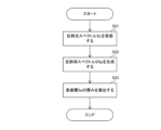
- FIG. 21 is a flowchart showing an example of an operational procedure for a thickness calculation device according to a second embodiment of the present invention to calculate the thickness of a surface layer.
- the thickness calculation device 202 receives from the spectrometer 101 the reflected light spectrum SL from the target sample P of the light irradiated from the surface layer Sa side of the target sample P (step S21).
- the thickness calculation device 202 Based on the reflected light spectrum SL, the thickness calculation device 202 generates a reflectance spectrum SRp in a wavelength range Rr where the round-trip internal transmittance Ia(d) of the surface layer Sa is equal to or greater than the threshold value Th1, and the round-trip internal transmittance Iab(d) of the layer consisting of the surface layer Sa and the adjacent lower layer Sb is equal to or less than the threshold value Th1 (step S22).
- the thickness calculation device 202 calculates the thickness of the surface layer Sa based on the reflectance spectrum SRp (step S23).
Landscapes
- Physics & Mathematics (AREA)
- General Physics & Mathematics (AREA)
- Spectroscopy & Molecular Physics (AREA)
- Length Measuring Devices By Optical Means (AREA)
- Analytical Chemistry (AREA)
- Chemical & Material Sciences (AREA)
- Life Sciences & Earth Sciences (AREA)
- Biochemistry (AREA)
- General Health & Medical Sciences (AREA)
- Immunology (AREA)
- Pathology (AREA)
- Health & Medical Sciences (AREA)
- Mathematical Physics (AREA)
Abstract
Description
本発明は、分光器、厚み測定システム、厚み算出装置、分光器の製造方法および厚み算出方法に関する。 The present invention relates to a spectrometer, a thickness measurement system, a thickness calculation device, a method for manufacturing a spectrometer, and a method for calculating thickness.
従来、対象試料に光を照射し、対象試料の反射率スペクトルに基づいて、対象試料の厚みを測定するための技術が提案されている。 Conventionally, a technique has been proposed for measuring the thickness of a target sample based on the reflectance spectrum of the target sample by irradiating the target sample with light.
たとえば、特許文献1(特開2014-55780号公報)には、以下のような膜厚計測方法が開示されている。すなわち、膜厚計測方法は、光の透過率に差のある第1波長領域及び第2波長領域を有し、前記第1波長領域の方が前記第2波長領域よりも光の透過率が低い基準膜と、前記基準膜の一方側に形成された1又は複数の測定対象膜と、前記基準膜の他方側に形成された1または複数の測定対象膜と、を含む試料を用い、前記各測定対象膜の厚さを計測する膜厚計測方法であって、前記試料に前記一方側から光を照射する照射ステップと、前記試料による前記光の反射率スペクトルを、前記第1波長領域の一部又は全部、及び前記第2波長領域の一部又は全部において測定する測定ステップと、前記第1波長領域における反射率スペクトルに基づいて、前記一方側に形成された前記各測定対象膜の厚さを計算する第1計算ステップと、前記一方側に形成された前記各測定対象膜の厚さと、少なくとも前記第2波長領域における反射率スペクトルと、に基づいて、前記他方側に形成される前記各膜の厚さを計算する第2計算ステップとを含む。 For example, Patent Document 1 (JP Patent Publication 2014-55780A) discloses a film thickness measurement method as follows. That is, the film thickness measurement method uses a sample including a reference film having a first wavelength region and a second wavelength region with a difference in light transmittance, the first wavelength region having a lower light transmittance than the second wavelength region, one or more measurement target films formed on one side of the reference film, and one or more measurement target films formed on the other side of the reference film, and measures the thickness of each of the measurement target films, and includes an irradiation step of irradiating the sample with light from the one side, a measurement step of measuring the reflectance spectrum of the light by the sample in part or all of the first wavelength region and part or all of the second wavelength region, a first calculation step of calculating the thickness of each of the measurement target films formed on the one side based on the reflectance spectrum in the first wavelength region, and a second calculation step of calculating the thickness of each of the films formed on the other side based on the thickness of each of the measurement target films formed on the one side and the reflectance spectrum in at least the second wavelength region.
また、たとえば、特許文献2(特開2008-286583号公報)には、カセグレイン型の反射対物レンズを備える光学特性測定装置が開示されている。当該反射対物レンズは、中心軸が光軸と一致するように配置された凸面反射鏡および凹面反射鏡を含む。特許文献2に記載の光学特性測定装置では、被測定物の表面で反射して生じる測定反射光は、ピンホールを通過して分光測定部へ入射する一方で、被測定物の裏面で反射して生じる裏面反射光は、ピンホールを通過できない。したがって、特許文献2に記載の光学特性測定装置では、裏面反射光すなわち迷光の影響を回避することができる。
Also, for example, Patent Document 2 (JP 2008-286583 A) discloses an optical property measuring device equipped with a Cassegrain-type reflective objective lens. The reflective objective lens includes a convex reflector and a concave reflector arranged so that the central axis coincides with the optical axis. In the optical property measuring device described in
特許文献1および2に記載の技術を超えて、多層構造の対象試料における表面層の厚みをより正確に測定することが可能な技術が望まれる。
There is a need for a technology that goes beyond the technology described in
本発明は、上述の課題を解決するためになされたもので、その目的は、多層構造の対象試料における表面層の厚みをより正確に測定することが可能な分光器、厚み測定システム、厚み算出装置、分光器の製造方法および厚み算出方法を提供することである。 The present invention has been made to solve the above-mentioned problems, and its purpose is to provide a spectrometer, a thickness measurement system, a thickness calculation device, a method for manufacturing a spectrometer, and a thickness calculation method that are capable of more accurately measuring the thickness of the surface layer of a target sample with a multi-layer structure.
(1)上記課題を解決するために、この発明のある局面に係わる分光器は、表面層と下層とが積層された多層構造の対象試料における、前記表面層の厚みの測定に用いられる分光器であって、前記対象試料の前記表面層側から照射された光の前記対象試料からの反射光を受光する受光部と、前記反射光を分光することにより反射光スペクトルを生成する分光部とを備え、前記分光部は、前記表面層の往復内部透過率が所定の下限値以上となり、かつ前記表面層と前記下層とを合わせた層の往復内部透過率が所定の上限値以下となる分光波長範囲における前記反射光スペクトルを生成する。 (1) In order to solve the above problem, a spectrometer according to one aspect of the present invention is a spectrometer used to measure the thickness of a surface layer of a target sample having a multilayer structure in which a surface layer and an underlayer are stacked, and includes a light receiving section that receives light reflected from the target sample of light irradiated from the surface layer side of the target sample, and a spectroscopic section that generates a reflected light spectrum by dispersing the reflected light, and the spectroscopic section generates the reflected light spectrum in a spectral wavelength range in which the round-trip internal transmittance of the surface layer is equal to or greater than a predetermined lower limit, and the round-trip internal transmittance of the layer consisting of the surface layer and the underlayer is equal to or less than a predetermined upper limit.
このように、表面層の往復内部透過率の下限値と、表面層と下層とを合わせた層の往復内部透過率の上限値とを設定し、表面層の往復内部透過率が下限値以上となり、かつ表面層と下層とを合わせた層の往復内部透過率が上限値以下となる分光波長範囲における反射光スペクトルを生成する構成により、表面層の光照射面おける反射光の成分および表面層と下層との界面における反射光の成分を含む一方で、当該下層における当該界面とは反対側の界面における反射光の成分が低減された反射光スペクトルを生成することができる。そのため、当該反射光スペクトルを用いて生成された、表面層の干渉波形である反射率スペクトルに基づいて、表面層の厚みをより正確に算出することができる。したがって、多層構造の対象試料における表面層の厚みをより正確に測定することができる。ここで、「往復内部透過率I(d)」とは、厚みdの層に入射した光が入射面と反対側の界面すなわち裏面で反射し、入射面に戻る成分に相当し、当該層における往復過程の材料吸収による減衰を透過率として表したものである。 In this way, by setting a lower limit of the round-trip internal transmittance of the surface layer and an upper limit of the round-trip internal transmittance of the layer formed by combining the surface layer and the lower layer, and generating a reflected light spectrum in a spectral wavelength range in which the round-trip internal transmittance of the surface layer is equal to or greater than the lower limit and the round-trip internal transmittance of the layer formed by combining the surface layer and the lower layer is equal to or less than the upper limit, a reflected light spectrum can be generated that includes the components of reflected light at the light-irradiated surface of the surface layer and the components of reflected light at the interface between the surface layer and the lower layer, while reducing the components of reflected light at the interface on the opposite side of the interface in the lower layer. Therefore, the thickness of the surface layer can be calculated more accurately based on the reflectance spectrum, which is the interference waveform of the surface layer generated using the reflected light spectrum. Therefore, the thickness of the surface layer in a target sample with a multilayer structure can be measured more accurately. Here, the "round-trip internal transmittance I(d)" corresponds to the component of light incident on a layer of thickness d that is reflected at the interface opposite to the incident surface, i.e., the back surface, and returns to the incident surface, and is the attenuation due to material absorption in the round-trip process in the layer expressed as transmittance.
(2)上記(1)において、前記分光部は、前記表面層の厚み範囲において、前記表面層の往復内部透過率が所定の閾値以上であり、かつ前記表面層と前記下層とを合わせた層の往復内部透過率が前記閾値以下となる前記分光波長範囲における前記反射光スペクトルを生成してもよい。 (2) In the above (1), the spectroscopic unit may generate the reflected light spectrum in the spectroscopic wavelength range in which, within the thickness range of the surface layer, the round-trip internal transmittance of the surface layer is equal to or greater than a predetermined threshold, and the round-trip internal transmittance of the combined layer of the surface layer and the lower layer is equal to or less than the threshold.
このような構成により、ノイズおよびダイナミックレンジ等に基づく検出限界を考慮して、厚み測定においてより有効な反射光スペクトルを生成することができる。具体的には、たとえば、表面層と下層との界面において反射された反射光のレベルがノイズレベル以上であり、かつ、下層と他の下層との界面において反射された反射光のレベルが当該ノイズレベル以下となる反射光スペクトルを生成することができる。 With this configuration, it is possible to generate a reflected light spectrum that is more effective in thickness measurement, taking into account detection limits based on noise, dynamic range, etc. Specifically, for example, it is possible to generate a reflected light spectrum in which the level of reflected light reflected at the interface between the surface layer and the lower layer is equal to or higher than the noise level, and the level of reflected light reflected at the interface between the lower layer and another lower layer is equal to or lower than the noise level.
(3)上記(1)または(2)において、前記表面層は、シリコン層であってもよく、前記分光部は、650nm以上であり、かつ800nm以下の前記分光波長範囲における前記反射光スペクトルを生成してもよい。 (3) In the above (1) or (2), the surface layer may be a silicon layer, and the spectroscopic unit may generate the reflected light spectrum in the spectroscopic wavelength range of 650 nm or more and 800 nm or less.
このような構成により、多層構造の主表面を構成するシリコン層の厚みをより正確に測定することができる。 This configuration allows for more accurate measurement of the thickness of the silicon layer that constitutes the main surface of the multi-layer structure.
(4)上記課題を解決するために、この発明のある局面に係わる厚み測定システムは、上記(1)から(3)のいずれかの分光器と、光源からの光を前記対象試料の前記表面層側から照射し、かつ照射した光の前記対象試料からの前記反射光を前記分光器へ導くマクロ光学系とを備える。 (4) In order to solve the above problem, a thickness measurement system according to a certain aspect of the present invention includes a spectrometer as described above in (1) to (3), and a macro-optical system that irradiates the surface layer side of the target sample with light from a light source and guides the reflected light from the target sample to the spectrometer.
このような構成により、特許文献2に記載されている光学特性測定装置等の顕微分光膜厚計と比べて、より高速に表面層の厚みを測定することができる。
This configuration allows the thickness of the surface layer to be measured more quickly than a microspectrophotometer such as the optical property measuring device described in
(5)上記課題を解決するために、この発明のある局面に係わる厚み算出装置は、表面層と下層とが積層された多層構造の対象試料における、前記表面層の厚みの測定に用いられる厚み算出装置であって、前記対象試料の前記表面層側から照射された光の前記対象試料からの反射光の反射光スペクトルを取得する取得部と、前記取得部により取得された前記反射光スペクトルに基づいて、前記対象試料の反射率スペクトルを生成する生成部と、前記生成部により生成された前記反射率スペクトルに基づいて、前記表面層の厚みを算出する算出部とを備え、前記生成部は、前記表面層の往復内部透過率が所定の下限値以上となり、かつ前記表面層と前記下層とを合わせた層の往復内部透過率が所定の上限値以下となる波長範囲における前記反射率スペクトルを生成する。 (5) In order to solve the above problem, a thickness calculation device according to one aspect of the present invention is a thickness calculation device used to measure the thickness of a surface layer of a target sample having a multilayer structure in which a surface layer and a lower layer are stacked, and includes an acquisition unit that acquires a reflected light spectrum of light reflected from the target sample by light irradiated from the surface layer side of the target sample, a generation unit that generates a reflectance spectrum of the target sample based on the reflected light spectrum acquired by the acquisition unit, and a calculation unit that calculates the thickness of the surface layer based on the reflectance spectrum generated by the generation unit, and the generation unit generates the reflectance spectrum in a wavelength range in which the round-trip internal transmittance of the surface layer is equal to or greater than a predetermined lower limit and the round-trip internal transmittance of the layer consisting of the surface layer and the lower layer is equal to or less than a predetermined upper limit.
このように、対象試料の反射光の反射光スペクトルに基づいて、表面層の往復内部透過率が所定の下限値以上となり、かつ表面層と下層とを合わせた層の往復内部透過率が上限値以下となる波長範囲における反射率スペクトルを生成し、当該反射率スペクトルに基づいて厚みを算出する構成により、表面層の光照射面における反射光の成分および表面層と下層との界面における反射光の成分を含む一方で、当該下層における当該界面とは反対側の界面における反射光の成分が低減された反射率スペクトルを生成することができる。そのため、生成した反射率スペクトルを用いて、表面層の厚みをより正確に算出することができる。したがって、多層構造の対象試料における表面層の厚みをより正確に測定することができる。 In this way, a reflectance spectrum is generated in a wavelength range where the round-trip internal transmittance of the surface layer is equal to or greater than a predetermined lower limit and the round-trip internal transmittance of the combined surface layer and lower layer is equal to or less than an upper limit based on the reflected light spectrum of the reflected light of the target sample, and the thickness is calculated based on the reflectance spectrum. This makes it possible to generate a reflectance spectrum that includes components of reflected light at the light-irradiated surface of the surface layer and components of reflected light at the interface between the surface layer and the lower layer, while reducing components of reflected light at the interface of the lower layer on the opposite side to the interface. Therefore, the thickness of the surface layer can be calculated more accurately using the generated reflectance spectrum. Therefore, the thickness of the surface layer of a target sample with a multilayer structure can be measured more accurately.
(6)上記(5)において、前記生成部は、前記表面層の厚み範囲において、前記表面層の往復内部透過率が所定の閾値以上であり、かつ前記表面層と前記下層とを合わせた層の往復内部透過率が前記閾値以下となる前記波長範囲における前記反射率スペクトルを生成してもよい。 (6) In the above (5), the generating unit may generate the reflectance spectrum in the wavelength range in which, within the thickness range of the surface layer, the round-trip internal transmittance of the surface layer is equal to or greater than a predetermined threshold, and the round-trip internal transmittance of the layer consisting of the surface layer and the lower layer is equal to or less than the threshold.
このような構成により、ノイズおよびダイナミックレンジ等に基づく検出限界を考慮して、厚み測定においてより有効な反射率スペクトルを生成することができる。具体的には、たとえば、表面層と下層との界面において反射された反射光のレベルがノイズレベル以上であり、かつ、下層と他の下層との界面において反射された反射光のレベルが当該ノイズレベル以下となる反射率スペクトルを生成することができる。 With this configuration, it is possible to generate a reflectance spectrum that is more effective in thickness measurement, taking into account detection limits based on noise, dynamic range, etc. Specifically, for example, it is possible to generate a reflectance spectrum in which the level of reflected light reflected at the interface between the surface layer and the lower layer is equal to or higher than the noise level, and the level of reflected light reflected at the interface between the lower layer and another lower layer is equal to or lower than the noise level.
(7)上記課題を解決するために、この発明のある局面に係わる分光器の製造方法は、表面層と下層とが積層された多層構造の対象試料における、前記表面層の厚みの測定に用いられる分光器の製造方法であって、波長と前記表面層の往復内部透過率との対応関係を示す第1の対応情報を取得するステップと、波長と、前記表面層および前記下層を合わせた層の往復内部透過率との対応関係を示す第2の対応情報を取得するステップと、取得した前記第1の対応情報および前記第2の対応情報に基づいて、前記対象試料の前記表面層側から照射された光の前記対象試料からの反射光を分光する前記分光器の分光波長範囲を設定するステップとを含み、前記分光波長範囲を設定するステップにおいては、前記表面層の往復内部透過率が所定の下限値以上となり、かつ前記表面層と前記下層とを合わせた層の往復内部透過率が所定の上限値以下となる前記分光波長範囲を設定する。 (7) In order to solve the above problem, a manufacturing method of a spectrometer according to a certain aspect of the present invention is a manufacturing method of a spectrometer used for measuring the thickness of a surface layer of a target sample having a multilayer structure in which a surface layer and a lower layer are stacked, and includes the steps of acquiring first correspondence information indicating the correspondence relationship between a wavelength and a round-trip internal transmittance of the surface layer, acquiring second correspondence information indicating the correspondence relationship between a wavelength and a round-trip internal transmittance of a layer formed by combining the surface layer and the lower layer, and setting a spectroscopic wavelength range of the spectrometer that splits light reflected from the target sample of light irradiated from the surface layer side of the target sample based on the acquired first correspondence information and second correspondence information, and in the step of setting the spectroscopic wavelength range, the spectroscopic wavelength range is set so that the round-trip internal transmittance of the surface layer is equal to or greater than a predetermined lower limit and the round-trip internal transmittance of the layer formed by combining the surface layer and the lower layer is equal to or less than a predetermined upper limit.
このように、表面層の往復内部透過率の下限値と、表面層と下層とを合わせた層の往復内部透過率の上限値とを設定し、表面層の往復内部透過率が下限値以上となり、かつ表面層と下層とを合わせた層の往復内部透過率が上限値以下となる分光波長範囲を設定する構成により、作製した分光器を用いて、表面層の光照射面における反射光の成分および表面層と下層との界面における反射光の成分を含む一方で、当該下層における当該界面とは反対側の界面における反射光の成分が低減された反射光スペクトルを生成することができる。そのため、当該反射光スペクトルを用いて生成された、表面層の干渉波形である反射率スペクトルを用いて、表面層の厚みをより正確に算出することができる。したがって、多層構造の対象試料における表面層の厚みをより正確に測定することができる。 In this way, by setting a lower limit value of the round-trip internal transmittance of the surface layer and an upper limit value of the round-trip internal transmittance of the layer formed by combining the surface layer and the lower layer, and setting a spectral wavelength range in which the round-trip internal transmittance of the surface layer is equal to or greater than the lower limit value and the round-trip internal transmittance of the layer formed by combining the surface layer and the lower layer is equal to or less than the upper limit value, it is possible to generate, using the manufactured spectrometer, a reflected light spectrum that includes components of reflected light at the light irradiation surface of the surface layer and components of reflected light at the interface between the surface layer and the lower layer, while reducing components of reflected light at the interface on the opposite side of the interface in the lower layer. Therefore, the thickness of the surface layer can be calculated more accurately using the reflectance spectrum, which is the interference waveform of the surface layer generated using the reflected light spectrum. Therefore, the thickness of the surface layer in a target sample having a multilayer structure can be measured more accurately.
(8)上記(7)において、前記分光器の製造方法は、さらに、前記表面層の厚み範囲を取得するステップを含んでもよく、前記分光波長範囲を設定するステップにおいては、前記表面層の厚みが前記厚み範囲の最大値である場合において前記表面層の往復内部透過率が所定の閾値になるときの波長である第1波長と、前記表面層の厚みが前記厚み範囲の最小値である場合において前記表面層と前記下層とを合わせた層の往復内部透過率が前記閾値になるときの波長である第2波長との間の波長範囲内において、前記分光波長範囲を設定してもよい。 (8) In the above (7), the method of manufacturing the spectrometer may further include a step of acquiring a thickness range of the surface layer, and in the step of setting the spectroscopic wavelength range, the spectroscopic wavelength range may be set within a wavelength range between a first wavelength, which is the wavelength at which the round-trip internal transmittance of the surface layer reaches a predetermined threshold value when the thickness of the surface layer is the maximum value of the thickness range, and a second wavelength, which is the wavelength at which the round-trip internal transmittance of the combined layer of the surface layer and the underlayer reaches the threshold value when the thickness of the surface layer is the minimum value of the thickness range.
このような構成により、ノイズおよびダイナミックレンジ等に基づく検出限界を考慮して、厚み測定においてより有効な反射光スペクトルを生成可能な分光器の仕様を決定することができる。具体的には、たとえば、表面層と下層との界面において反射された反射光のレベルがノイズレベル以上であり、かつ、下層と他の下層との界面において反射された反射光のレベルが当該ノイズレベル以下となる反射光スペクトルを生成可能な分光器の仕様を決定することができる。 With this configuration, it is possible to determine the specifications of a spectrometer capable of generating a reflected light spectrum that is more effective in thickness measurement, taking into account detection limits based on noise, dynamic range, etc. Specifically, for example, it is possible to determine the specifications of a spectrometer capable of generating a reflected light spectrum in which the level of reflected light reflected at the interface between the surface layer and the lower layer is equal to or higher than the noise level, and the level of reflected light reflected at the interface between the lower layer and another lower layer is equal to or lower than the noise level.
(9)上記課題を解決するために、この発明のある局面に係わる厚み算出方法は、表面層と下層とが積層された多層構造の対象試料における、前記表面層の厚みの測定に用いられる厚み算出装置における厚み算出方法であって、前記対象試料の前記表面層側から照射された光の前記対象試料からの反射光の反射光スペクトルを取得するステップと、取得した前記反射光スペクトルに基づいて、前記対象試料の反射率スペクトルを生成するステップと、生成した前記反射率スペクトルに基づいて、前記表面層の厚みを算出するステップとを含み、前記反射率スペクトルを生成するステップにおいては、前記表面層の往復内部透過率が所定の下限値以上となり、かつ前記表面層と前記下層とを合わせた層の往復内部透過率が所定の上限値以下となる波長範囲における前記反射率スペクトルを生成する。 (9) In order to solve the above problem, a thickness calculation method according to a certain aspect of the present invention is a thickness calculation method in a thickness calculation device used to measure the thickness of a surface layer of a target sample having a multilayer structure in which a surface layer and an underlayer are stacked, and includes the steps of acquiring a reflected light spectrum of light reflected from the target sample, the light being irradiated from the surface layer side of the target sample, generating a reflectance spectrum of the target sample based on the acquired reflected light spectrum, and calculating the thickness of the surface layer based on the generated reflectance spectrum, and in the step of generating the reflectance spectrum, the reflectance spectrum is generated in a wavelength range in which the round-trip internal transmittance of the surface layer is equal to or greater than a predetermined lower limit, and the round-trip internal transmittance of the combined layer of the surface layer and the underlayer is equal to or less than a predetermined upper limit.
このように、対象試料の反射光の反射光スペクトルに基づいて、表面層の往復内部透過率が所定の下限値以上となり、かつ表面層と下層とを合わせた層の往復内部透過率が上限値以下となる波長範囲における反射率スペクトルを生成し、当該反射率スペクトルに基づいて厚みを算出する方法により、表面層の光照射面における反射光の成分および表面層と下層との界面における反射光の成分を含む一方で、当該下層における当該界面とは反対側の界面における反射光の成分が低減された反射率スペクトルを生成することができる。そのため、生成した反射率スペクトルを用いて、表面層の厚みをより正確に算出することができる。したがって、多層構造の対象試料における表面層の厚みをより正確に測定することができる。 In this way, by generating a reflectance spectrum in a wavelength range where the round-trip internal transmittance of the surface layer is equal to or greater than a predetermined lower limit and the round-trip internal transmittance of the combined surface layer and lower layer is equal to or less than an upper limit based on the reflected light spectrum of the reflected light of the target sample, and calculating the thickness based on the reflectance spectrum, it is possible to generate a reflectance spectrum that includes components of reflected light at the light-irradiated surface of the surface layer and components of reflected light at the interface between the surface layer and the lower layer, while reducing components of reflected light at the interface of the lower layer on the opposite side to the interface. Therefore, the thickness of the surface layer can be calculated more accurately using the generated reflectance spectrum. Therefore, the thickness of the surface layer of a target sample with a multilayer structure can be measured more accurately.
本発明によれば、多層構造の対象試料における表面層の厚みをより正確に測定することができる。 The present invention makes it possible to more accurately measure the thickness of the surface layer of a multi-layered target sample.
以下、本発明の実施の形態について図面を用いて説明する。なお、図中同一または相当部分には同一符号を付してその説明は繰り返さない。また、以下に記載する実施の形態の少なくとも一部を任意に組み合わせてもよい。 Below, embodiments of the present invention will be described with reference to the drawings. Note that the same or corresponding parts in the drawings will be given the same reference numerals and their description will not be repeated. In addition, at least some of the embodiments described below may be combined in any manner.
<第1の実施の形態>
図1は、本発明の第1の実施の形態に係る厚み測定システムの構成を示す図である。図1を参照して、厚み測定システム301は、光源50と、マクロ光学系60と、分光器101と、厚み算出装置201とを備える。
First Embodiment
1 is a diagram showing a configuration of a thickness measurement system according to a first embodiment of the present invention. Referring to FIG. 1, the
厚み測定システム301は、分光干渉式の測定システムであり、表面層Saと下層Sbとが積層された多層構造の対象試料Pにおける表面層Saの厚みの測定に用いられる。表面層Saの表面は、対象試料Pの主表面Pmである。たとえば、測定対象の表面層Saの厚み範囲Rthの下限値は1μm以上であり、厚み範囲Rthの上限値は20μm以下である。対象試料Pの形状は、ウェハ形状であってもよいし、矩形形状であってもよいし、フィルム形状であってもよい。
The
対象試料Pは、表面層Saと、複数の下層Sbとを含む。たとえば、表面層Saはシリコン層であり、下層Sbは、シリコンオキサイド薄膜をコーティングしたシリコン層である。たとえば、対象試料Pは、下層Sbとして、表面層Sa側から、シリコンオキサイド薄膜をコーティングしたシリコン層が複数積層された繰り返し層構造を有する。言い換えると、対象試料Pは、下層Sbとして、表面層Sa側から、コーティングであるシリコンオキサイド層と、シリコン層とが交互に積層された繰り返し層構造を有する。なお、対象試料Pは、1つの下層Sbを含む構成であってもよい。以下では、表面層Saに隣接する下層Sb、すなわち表面層Saの直下の下層Sbを、「隣接下層Sb」とも称する。 The target sample P includes a surface layer Sa and multiple lower layers Sb. For example, the surface layer Sa is a silicon layer, and the lower layers Sb are silicon layers coated with a silicon oxide thin film. For example, the target sample P has a repeating layer structure in which multiple silicon layers coated with a silicon oxide thin film are stacked as the lower layers Sb from the surface layer Sa side. In other words, the target sample P has a repeating layer structure in which a silicon oxide layer, which is a coating, and a silicon layer are alternately stacked as the lower layers Sb from the surface layer Sa side. Note that the target sample P may be configured to include one lower layer Sb. Hereinafter, the lower layer Sb adjacent to the surface layer Sa, i.e., the lower layer Sb directly below the surface layer Sa, is also referred to as the "adjacent lower layer Sb".
光源50は、表面層Saの厚みの測定に用いる光を出射する。光源50は、複数波長を含む光を出射する。光源50が出射する光のスペクトルは、連続スペクトルである。光源50が出射する光の波長の範囲は、分光器101の分光波長範囲Rs1を含む。光源50は、たとえばハロゲンランプである。
The
マクロ光学系60は、光源50からの光を対象試料Pの表面層Sa側から照射し、かつ照射した光の対象試料Pからの反射光を分光器101へ導く。より詳細には、マクロ光学系60は、Y型光ファイバ61と、プローブ62とを含む。プローブ62は、Y型光ファイバ61の第1端に設けられる。Y型光ファイバ61の第2端は、二股に分岐している。Y型光ファイバ61の分岐部61Aは、光源50に接続される。Y型光ファイバ61の分岐部61Bは、分光器101に接続される。
The macro
光源50から出射される光は、Y型光ファイバ61およびプローブ62を介して対象試料Pの主表面Pmへ照射される。主表面Pmへ照射された光の対象試料Pからの反射光は、プローブ62およびY型光ファイバ61を介して分光器101へ導かれる。なお、厚み測定システム301は、マクロ光学系60の代わりに、レンズおよびビームスプリッタ等を含む光学系を備える構成であってもよい。
The light emitted from the
分光器101は、対象試料Pからの反射光を分光することにより、分光波長範囲Rs1を含む反射光スペクトルSLを生成する。一例として、分光器101は、対象試料Pからの反射光を分光することにより、分光波長範囲Rs1における反射光スペクトルSLを生成する。分光器101は、生成した反射光スペクトルSLを厚み算出装置201へ送信する。
The
図2は、本発明の第1の実施の形態に係る厚み算出装置の構成を示す図である。図2を参照して、厚み算出装置201は、受信部21と、生成部22と、算出部23とを備える。受信部21は、取得部の一例である。受信部21、生成部22および算出部23の一部または全部は、たとえば、1または複数のプロセッサを含む処理回路により実現される。
FIG. 2 is a diagram showing the configuration of a thickness calculation device according to a first embodiment of the present invention. Referring to FIG. 2, the
受信部21は、表面層Sa側から光を照射された対象試料Pからの反射光スペクトルSLを分光器101から受信し、受信した反射光スペクトルSLを生成部22へ出力する。
The
生成部22は、受信部21から受けた反射光スペクトルSLに基づいて、対象試料Pの反射率スペクトルSRを生成する。より詳細には、生成部22は、反射光スペクトルSLを、対象試料Pへ照射される光の照射光スペクトルで除することにより、反射率スペクトルSRを生成する。生成部22は、生成した反射率スペクトルSRを算出部23へ出力する。
The generating
算出部23は、生成部22により生成された反射率スペクトルSRに基づいて、表面層Saの厚みを算出する。たとえば、算出部23は、FFT(Fast Fourier Transform)法に従って反射率スペクトルSRを解析することにより、表面層Saの厚みを算出する。より詳細には、算出部23は、反射率スペクトルSRをFFT処理することにより、反射率スペクトルSRのパワースペクトルを生成する。そして、算出部23は、生成したパワースペクトルから、与えられた選択条件に適合する厚みを、表面層Saの厚みとして特定する。
The
[課題]
多層構造の対象試料Pにおける表面層Saの厚みをより正確に測定することが可能な技術が望まれる。
[assignment]
A technique capable of more accurately measuring the thickness of the surface layer Sa in a target sample P having a multi-layer structure is desired.
より詳細には、一般的に、分光干渉式の測定システムでは、膜の厚みを測定するために、外部から膜の主表面へ照射された光の当該膜からの反射光を分光することにより、当該膜の内部透過率の大きい波長範囲における反射率スペクトルSRを生成し、当該反射率スペクトルSRに基づいて厚みを算出することが好ましい。特に、比較的厚い膜の厚みを測定する場合、当該膜の内部透過率の大きい波長範囲における、光が照射される上記主表面とは反対側の面からの十分な強度の反射光を示す反射率スペクトルSRに基づいて厚みを算出することが好ましい。 More specifically, in general, in order to measure the thickness of a film, in a spectral interference measurement system, it is preferable to generate a reflectance spectrum SR in a wavelength range in which the internal transmittance of the film is high by dispersing light reflected from the film when light is irradiated from the outside onto the main surface of the film, and to calculate the thickness based on the reflectance spectrum SR. In particular, when measuring the thickness of a relatively thick film, it is preferable to calculate the thickness based on a reflectance spectrum SR that shows reflected light of sufficient intensity from the surface opposite the main surface on which the light is irradiated, in a wavelength range in which the internal transmittance of the film is high.
そのため、従来の厚み測定システムは、たとえばシリコン膜の厚みを測定する場合、シリコン膜における消衰係数がゼロに近い値となる1000nm以上の分光波長範囲を有する分光器を用いて反射光スペクトルSLを生成し、生成した反射光スペクトルSLに基づいてシリコン層の厚みを算出する。 Therefore, when measuring the thickness of a silicon film, for example, a conventional thickness measurement system generates a reflected light spectrum SL using a spectrometer with a spectral wavelength range of 1000 nm or more, where the extinction coefficient of the silicon film is close to zero, and calculates the thickness of the silicon layer based on the generated reflected light spectrum SL.
図3から図8は、比較例に係る厚み測定システムによる対象試料の厚み測定のシミュレーション結果を示す図である。 Figures 3 to 8 show the simulation results of thickness measurement of a target sample using a thickness measurement system according to a comparative example.
図3から図5は、1000nm以上の分光波長範囲と、充分な波長分解能とを有する分光器を備える、比較例に係る厚み測定システムにおいて生成される反射率スペクトルSRを示している。図3から図5において、横軸は波長[nm]であり、縦軸は反射率である。図3は、表面層Saとして1μmのシリコン層を含み、かつ、下層Sbとして表面層Sa側から5μmのシリコンオキサイド層および21μmのシリコン層を交互に6層ずつ含む対象試料P1の反射率スペクトルSRを示している。図4は、対象試料P1と比べて、表面層Saとして10μmのシリコン層を含む対象試料P2の反射率スペクトルSRを示している。図5は、対象試料P1と比べて、表面層Saとして20μmのシリコン層を含む対象試料P3の反射率スペクトルSRを示している。 Figures 3 to 5 show reflectance spectra SR generated in a comparative thickness measurement system equipped with a spectrometer having a spectral wavelength range of 1000 nm or more and sufficient wavelength resolution. In Figures 3 to 5, the horizontal axis is wavelength [nm] and the vertical axis is reflectance. Figure 3 shows the reflectance spectrum SR of a target sample P1 that includes a 1 μm silicon layer as a surface layer Sa and includes six alternating layers of 5 μm silicon oxide layers and 21 μm silicon layers from the surface layer Sa side as lower layers Sb. Figure 4 shows the reflectance spectrum SR of a target sample P2 that includes a 10 μm silicon layer as a surface layer Sa compared to the target sample P1. Figure 5 shows the reflectance spectrum SR of a target sample P3 that includes a 20 μm silicon layer as a surface layer Sa compared to the target sample P1.
図6から図8は、比較例に係る厚み測定システムにおいて生成されるパワースペクトルを示している。図6から図8において、横軸は厚み[μm]であり、縦軸は強度である。図6から図8は、それぞれ、図3から図5に示す反射率スペクトルSRのパワースペクトルを示している。 FIGS. 6 to 8 show power spectra generated in a thickness measurement system according to a comparative example. In FIG. 6 to FIG. 8, the horizontal axis represents thickness [μm] and the vertical axis represents intensity. FIG. 6 to FIG. 8 show the power spectra of the reflectance spectrum SR shown in FIG. 3 to FIG. 5, respectively.
図6から図8を参照して、比較例に係る厚み測定システムは、対象試料P1の表面層Saの厚みを正確に測定することができない。より詳細には、比較例に係る厚み測定システムにより生成される対象試料P1,P2,P3のパワースペクトルにおいて、強度の最大値に対応する厚みは約2μmである。したがって、比較例に係る厚み測定システムによる表面層Saの厚みの測定結果は、実際の表面層Saの厚みが1μm、10μmまたは20μmであるにも関わらず、約2μmとなる。 Referring to Figures 6 to 8, the thickness measurement system according to the comparative example cannot accurately measure the thickness of the surface layer Sa of the target sample P1. More specifically, in the power spectra of the target samples P1, P2, and P3 generated by the thickness measurement system according to the comparative example, the thickness corresponding to the maximum intensity is approximately 2 μm. Therefore, the measurement result of the thickness of the surface layer Sa by the thickness measurement system according to the comparative example is approximately 2 μm, even though the actual thickness of the surface layer Sa is 1 μm, 10 μm, or 20 μm.
このように、比較例に係る厚み測定システムを用いて、多層構造を有する対象試料P1,P2,P3の厚みを測定する場合、表面層Saの厚みを測定することは困難である。また、仮に、反射率スペクトルSRを層ごとに分離できたとしても、反射率スペクトルSRに基づいて算出される厚みがどの層の厚みを示しているかを特定することは困難である。 As described above, when the thickness of the target samples P1, P2, and P3 having a multilayer structure is measured using the thickness measurement system according to the comparative example, it is difficult to measure the thickness of the surface layer Sa. Furthermore, even if the reflectance spectrum SR could be separated into layers, it is difficult to identify which layer the thickness calculated based on the reflectance spectrum SR indicates.
また、特許文献1に記載の技術では、基板となる膜が、所定の波長帯において、コートする膜の透過率よりも小さい透過率を有する必要があり、コートする膜が基板膜よりも透過率が小さい場合は測定出来ない。なお、特許文献1に記載の技術では、基板膜の片側に複数の層が積層されている場合において、当該複数の層のうちの表面層の厚みを測定する事は出来ない。
In addition, the technology described in
また、特許文献2には、カセグレイン型の反射対物レンズを用いることにより、被測定物の裏面からの光が迷光として現れることを抑制する技術が記載されている。しかしながら、特許文献2に記載の技術では、設計上の制約が大きい。
そこで、本発明の実施の形態に係る厚み測定システム301は、以下のような構成により、上記の課題を解決する。
The
(分光器)
図9は、本発明の第1の実施の形態に係る分光器の構成を示す図である。図9を参照して、分光器101は、スリット11と、分光部12とを備える。分光部12は、回折格子12Aと、検出部12Bと、コリメートミラー12Cと、フォーカスミラー12Dとを含む。スリット11は、受光部の一例である。
(Spectrometer)
Fig. 9 is a diagram showing the configuration of a spectrometer according to a first embodiment of the present invention. Referring to Fig. 9,
スリット11は、対象試料Pの表面層Sa側から照射された光の対象試料Pからの反射光を受光する。より詳細には、スリット11は、Y型光ファイバ61における分岐部61Bを介して、対象試料Pからの反射光を受光する。スリット11から分光器101の内部に入射した対象試料Pからの反射光は、コリメートミラー12Cにより平行光に整えられる。
The
分光部12は、対象試料Pからの反射光を分光することにより反射光スペクトルSLを生成する。
The
より詳細には、コリメートミラー12Cにより平行光に整えられた光は、回折格子12Aに導かれる。回折格子12Aは、入射した光を波長毎に異なる回折角で分光する。
More specifically, the light that has been collimated by the
回折格子12Aにより波長毎に異なる角度へと分光された光は、フォーカスミラー12Dによって検出部12Bにおける波長毎に異なる位置へ結像する。
The light split into different angles for each wavelength by the
たとえば、検出部12Bは、直線状に配列された複数の検出素子により構成されるリニアイメージセンサである。このような検出素子は、たとえば、CCD(Charge Coupled Device)イメージセンサまたはCMOS(Complementary Metal Oxide Semiconductor)イメージセンサである。検出部12Bにおける各検出素子は、回折格子12Aによって分光され、かつフォーカスミラー12Dによって結像された光を受光する。
For example, the
検出部12Bは、各検出素子の受光面において受光した光の、波長と強度との関係を示す反射光スペクトルSLを生成し、生成した反射光スペクトルSLを厚み算出装置201へ送信する。
The
たとえば、分光部12により生成される反射光スペクトルSLの波長分解能は、以下の式(1)および式(2)を満たす。

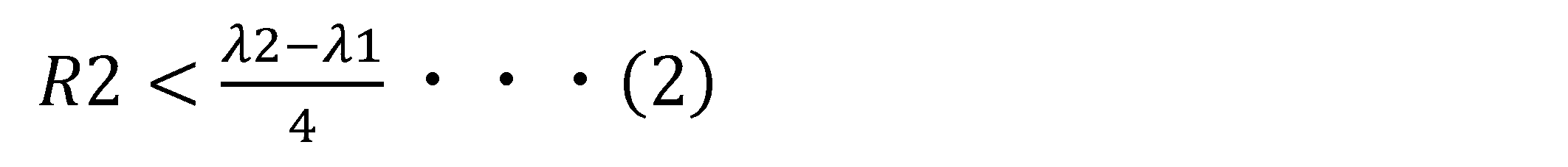
ここで、R1は、光学分解能である。R2は、画素分解能である。λ1は、反射光スペクトルSLにおける強度の極大値M1に対応する波長である。λ2は、反射光スペクトルSLにおける強度の極大値M2に対応する波長である。極大値M2は、極大値M1よりも大きく、かつ極大値M1に隣接する極大値である。 Here, R1 is the optical resolution. R2 is the pixel resolution. λ1 is the wavelength corresponding to the maximum intensity value M1 in the reflected light spectrum SL. λ2 is the wavelength corresponding to the maximum intensity value M2 in the reflected light spectrum SL. Maximum value M2 is a maximum value that is greater than and adjacent to maximum value M1.
分光部12は、表面層Saの往復内部透過率I(d)である往復内部透過率Ia(d)が所定の下限値以上となり、かつ表面層Saと隣接下層Sbとを合わせた層の往復内部透過率I(d)である往復内部透過率Iab(d)が所定の上限値以下となる分光波長範囲Rs1における反射光スペクトルSLを生成する。ここで、往復内部透過率Iab(d)は、表面層Saの厚みと、隣接下層Sbにおけるシリコン層の厚みとを合計した厚みを有するシリコン層の往復内部透過率に相当する。
The
図10は、往復内部透過率のシミュレーション結果を示す図である。図10において、横軸は波長[nm]であり、縦軸は往復内部透過率である。図10における実線は、1μmのシリコン層の往復内部透過率I(d)である往復内部透過率I(1)を示している。図10における破線は、20μmのシリコン層の往復内部透過率I(d)である往復内部透過率I(20)を示している。図10における一点鎖線は、21μmのシリコン層の往復内部透過率I(d)である往復内部透過率I(21)を示している。ここで、往復内部透過率I(1)は、1μmのシリコン層の往復の内部透過率であるので、2μmのシリコン層の内部透過率に相当する。また、往復内部透過率I(20)は、20μmのシリコン層の往復の内部透過率であるので、40μmのシリコン層の内部透過率に相当する。また、往復内部透過率I(21)は、21μmのシリコン層の往復の内部透過率であるので、42μmのシリコン層の内部透過率に相当する。 FIG. 10 is a diagram showing the simulation results of the round-trip internal transmittance. In FIG. 10, the horizontal axis is the wavelength [nm], and the vertical axis is the round-trip internal transmittance. The solid line in FIG. 10 indicates the round-trip internal transmittance I(1), which is the round-trip internal transmittance I(d) of a 1 μm silicon layer. The dashed line in FIG. 10 indicates the round-trip internal transmittance I(20), which is the round-trip internal transmittance I(d) of a 20 μm silicon layer. The dashed line in FIG. 10 indicates the round-trip internal transmittance I(21), which is the round-trip internal transmittance I(d) of a 21 μm silicon layer. Here, the round-trip internal transmittance I(1) is the round-trip internal transmittance of a 1 μm silicon layer, so it corresponds to the internal transmittance of a 2 μm silicon layer. Also, the round-trip internal transmittance I(20) is the round-trip internal transmittance of a 20 μm silicon layer, so it corresponds to the internal transmittance of a 40 μm silicon layer. Furthermore, the round-trip internal transmittance I(21) is the round-trip internal transmittance of a 21 μm silicon layer, which corresponds to the internal transmittance of a 42 μm silicon layer.
図10を参照して、分光部12は、厚み範囲Rthにおいて、表面層Saの往復内部透過率Ia(d)が所定の閾値Th1以上となり、かつ表面層Saと隣接下層Sbとを合わせた層の往復内部透過率Iab(d)が閾値Th1以下となる分光波長範囲Rs1における反射光スペクトルSLを生成する。閾値Th1は、下限値の一例であり、かつ上限値の一例である。
Referring to FIG. 10, the
一例として、分光波長範囲Rs1は、隣接下層Sbの厚みの設計値が20μmであり、表面層Saの厚みの設計値が1μmである場合、表面層Saの往復内部透過率Ia(1)が閾値Th1になるときの波長λaと、表面層Saと隣接下層Sbとを合わせた層の往復内部透過率Iab(21)が閾値Th1になるときの波長λbとの間の波長範囲内において設定される。波長λaは、第1波長の一例である。波長λbは、第2波長の一例である。閾値Th1は、1未満の値である。閾値Th1は、たとえば0.001である。なお、分光波長範囲Rs1は、往復内部透過率Ia(1)が閾値Th1になるときの波長λaと、往復内部透過率Iab(21)が閾値Th1とは異なる閾値Th2になるときの波長λbとの間の波長範囲内において設定されてもよい。 As an example, when the design value of the thickness of the adjacent lower layer Sb is 20 μm and the design value of the thickness of the surface layer Sa is 1 μm, the spectral wavelength range Rs1 is set within the wavelength range between the wavelength λa when the round-trip internal transmittance Ia(1) of the surface layer Sa becomes the threshold value Th1 and the wavelength λb when the round-trip internal transmittance Iab(21) of the layer including the surface layer Sa and the adjacent lower layer Sb becomes the threshold value Th1. The wavelength λa is an example of the first wavelength. The wavelength λb is an example of the second wavelength. The threshold value Th1 is a value less than 1. The threshold value Th1 is, for example, 0.001. Note that the spectral wavelength range Rs1 may be set within the wavelength range between the wavelength λa when the round-trip internal transmittance Ia(1) becomes the threshold value Th1 and the wavelength λb when the round-trip internal transmittance Iab(21) becomes the threshold value Th2 different from the threshold value Th1.
また、たとえば、分光部12は、厚み範囲Rthにおいて、表面層Saの往復内部透過率Ia(d)が厚み算出装置201におけるノイズレベル以上であり、かつ、表面層Saおよび隣接下層Sbを合わせた往復内部透過率Iab(d)が厚み算出装置201におけるノイズレベル以下となる分光波長範囲Rs1における反射光スペクトルSLを生成する。すなわち、分光部12は、厚み範囲Rthにおいて、表面層Saを透過して表面層Saと隣接下層Sbとの界面において反射された反射光のレベルが厚み算出装置201におけるノイズレベル以上であり、かつ、表面層Saおよび隣接下層Sbを透過して隣接下層Sbと他の下層Sbとの界面において反射された反射光のレベルが厚み算出装置201におけるノイズレベル以下となる分光波長範囲Rs1における反射光スペクトルSLを生成する。
Furthermore, for example, the
より詳細には、分光波長範囲Rs1は、往復内部透過率Ia(d)が厚み算出装置201におけるノイズレベル以上となる波長範囲において、FFT解析に充分な干渉波数が得られる波長範囲であり、かつ、表面層Saおよび隣接下層Sbを合わせた往復内部透過率Iab(d)が厚み算出装置201におけるノイズレベル以下となる波長範囲である。
More specifically, the spectral wavelength range Rs1 is a wavelength range in which the round-trip internal transmittance Ia(d) is equal to or greater than the noise level in the
たとえば、分光波長範囲Rs1は、波長に対する表面層Saの往復内部透過率の変化量の絶対値が所定値以上の波長範囲である。すなわち、分光部12の分光波長範囲Rs1は、表面層Saの往復内部透過率Ia(d)の変化がほとんど無い波長λc以上の波長を含まない波長範囲であり、ほとんど透過しない紫外域も含まない波長範囲である。言い換えると、分光部12の分光波長範囲Rs1は、波長λcよりも小さい波長範囲である。また、たとえば、分光波長範囲Rs1は、可視光領域の少なくとも一部を含む。
For example, the spectral wavelength range Rs1 is a wavelength range in which the absolute value of the change in the round-trip internal transmittance of the surface layer Sa with respect to wavelength is equal to or greater than a predetermined value. In other words, the spectral wavelength range Rs1 of the
また、たとえば、分光部12の分光波長範囲Rs1は、波長に対する、表面層Saを構成する材料の消衰係数の変化量の絶対値が所定値以上の波長範囲である。すなわち、分光部12の分光波長範囲Rs1は、表面層Saを構成する材料であるシリコンの消衰係数の低下が収束するときの波長よりも短い波長範囲であり、消衰係数が極端に大きい範囲を含まない波長範囲である。
Furthermore, for example, the spectroscopic wavelength range Rs1 of the
図11は、シリコンの消衰係数を示す図である。図11において、横軸は波長[nm]であり、縦軸は消衰係数である。図11を参照して、分光器101の設計者は、仕様決定の為に、以下のような処理を行う。すなわち、分光器101の設計者は、表面層Saおよび隣接下層Sbを構成する材料であるシリコンの消衰係数を取得する。
FIG. 11 is a diagram showing the extinction coefficient of silicon. In FIG. 11, the horizontal axis is wavelength [nm] and the vertical axis is extinction coefficient. With reference to FIG. 11, the designer of the
また、分光器101の設計者は、測定対象である表面層Saの厚み範囲Rthを取得する。厚み範囲Rthは、厚み測定システム301が測定可能な厚みの範囲である。分光器101の設計者は、対象試料Pに応じた厚み範囲Rthを設定してもよいし、厚み測定システム301のユーザの要望に応じた厚み範囲Rthを設定してもよい。また、たとえば、分光器101の設計者は、隣接下層Sbの厚み範囲をさらに取得する。
The designer of the
そして、分光器101の設計者は、取得した消衰係数および厚み範囲Rthに基づいて、表面層Saへ入射する光の波長と、当該表面層Saの往復内部透過率Ia(d)との対応関係を示す対応情報X1を作成する。また、分光器101の設計者は、取得した消衰係数、厚み範囲Rthおよび隣接下層Sbの厚みに基づいて、表面層Saへ入射する光の波長と、表面層Saおよび隣接下層Sbを合わせた層の往復内部透過率Iab(d)との対応関係を示す対応情報X2を作成する。たとえば、分光器101の設計者は、以下の式(3)に従って、厚み範囲Rthの下限値における往復内部透過率Ia(d)と、厚み範囲Rthの上限値における往復内部透過率Ia(d)とを算出する。
![]()
![]()
ここで、dは、表面層Saの厚みである。αは、吸光係数であり、以下の式(4)により表される。

ここで、λは、光源50から表面層Saへ照射される光の波長である。k(λ)は、波長λの光の消衰係数である。
Here, λ is the wavelength of light irradiated from the
分光器101の設計者は、対応情報X1,X2に基づいて、表面層Saの往復内部透過率I(d)が閾値Th1以上となり、かつ表面層Saと隣接下層Sbとを合わせた層の往復内部透過率Iab(d)が閾値Th1以下となる分光波長範囲Rs1を設定する。一例として、分光器101の設計者は、上述したように、往復内部透過率Ia(1)が閾値Th1になるときの波長λaと、往復内部透過率Iab(21)が閾値Th1になるときの波長λbとの間の波長範囲内において、分光波長範囲Rs1を設定する。
The designer of the
たとえば、分光器101の設計者は、対応情報X1,X2に基づいて、表面層Saの往復内部透過率Ia(d)が厚み算出装置201におけるノイズレベル以上であり、表面層Saおよび隣接下層Sbを合わせた往復内部透過率Iab(d)が厚み算出装置201におけるノイズレベル以下であり、かつFFT解析に充分な数の表面層Saの干渉波数が得られる分光波長範囲Rs1を設定する。すなわち、表面層Saおよび隣接下層Sbを合わせた往復内部透過率Iab(d)が、表面層Saから得られる干渉波形をFFT解析したパワースペクトルに影響を与えないレベルの干渉波形しか得られないような分光波長範囲Rs1を設定する。
For example, the designer of the
図12から図14は、本発明の第1の実施の形態に係る厚み測定システムにおいて生成される反射率スペクトルSRを示している。図12から図14は、表面層Saの厚み範囲Rthに基づいて設定された、650nm以上であり、かつ800nm以下の分光波長範囲Rs1を有する分光器101を備える厚み測定システム301において生成される反射率スペクトルSRを示している。図12から図14において、横軸は波長[nm]であり、縦軸は反射率である。図12から図14は、それぞれ、上述した対象試料P1,P2,P3の反射率スペクトルSRを示している。
FIGS. 12 to 14 show reflectance spectra SR generated in a thickness measurement system according to a first embodiment of the present invention. FIGS. 12 to 14 show reflectance spectra SR generated in a
図15から図17は、本発明の第1の実施の形態に係る厚み測定システムにおいて生成されるパワースペクトルを示している。図15から図17において、横軸は厚み[μm]であり、縦軸は強度である。図15から図17は、それぞれ、図12から図14に示す反射率スペクトルSRのパワースペクトルを示している。 FIGS. 15 to 17 show power spectra generated in a thickness measurement system according to a first embodiment of the present invention. In FIG. 15 to FIG. 17, the horizontal axis represents thickness [μm] and the vertical axis represents intensity. FIG. 15 to FIG. 17 show the power spectra of the reflectance spectrum SR shown in FIG. 12 to FIG. 14, respectively.
図15から図17を参照して、厚み測定システム301は、対象試料P1の表面層Saの厚みを正確に測定することができる。
Referring to Figures 15 to 17, the
より詳細には、厚み測定システム301により生成される対象試料P1のパワースペクトルにおいて、強度の最大値に対応する厚みは約1μmである。したがって、厚み測定システム301による表面層Saの厚みの測定結果は、実際の表面層Saの厚みとほぼ等しい値となる。
More specifically, in the power spectrum of the target sample P1 generated by the
また、厚み測定システム301により生成される対象試料P2のパワースペクトルにおいて、強度の最大値に対応する厚みは約10μmである。したがって、厚み測定システム301による表面層Saの厚みの測定結果は、実際の表面層Saの厚みとほぼ等しい値となる。
In addition, in the power spectrum of the target sample P2 generated by the
また、厚み測定システム301により生成される対象試料P3のパワースペクトルにおいて、強度の最大値に対応する厚みは約20μmである。したがって、厚み測定システム301による表面層Saの厚みの測定結果は、実際の表面層Saの厚みとほぼ等しい値となる。
In addition, in the power spectrum of the target sample P3 generated by the
図18は、本発明の第1の実施の形態に係る厚み測定システムにおける分光器の製造方法を示すフローチャートである。分光器101の設計者は、仕様決定の為に、以下のような処理を行う。
FIG. 18 is a flowchart showing a method for manufacturing a spectrometer in a thickness measurement system according to a first embodiment of the present invention. The designer of the
図18を参照して、まず、分光器101の設計者は、表面層Saおよび隣接下層Sbを構成する材料であるシリコンの消衰係数を取得する(ステップS11)。
Referring to FIG. 18, first, the designer of the
次に、分光器101の設計者は、測定対象である表面層Saの厚み範囲Rth、および隣接下層Sbの厚みの設計値を取得する(ステップS12)。
Next, the designer of the
次に、分光器101の設計者は、消衰係数および厚み範囲Rthに基づいて、表面層Saへ入射する光の波長と、当該表面層Saの往復内部透過率Ia(d)との対応関係を示す対応情報X1を作成する。対応情報X1は、FFT解析に充分な数の表面層Saの干渉波数が得られる波長範囲、ならびに分光器分解能を示す情報である。たとえば、分光器101の設計者は、厚み範囲Rthの下限値における表面層Saの往復内部透過率Ia(1)と、厚み範囲Rthの上限値における表面層Saの往復内部透過率Ia(20)とを算出する(ステップS13)。
Next, the designer of the
次に、分光器101の設計者は、消衰係数、厚み範囲Rthおよび隣接下層Sbの厚みに基づいて、表面層Saへ入射する光の波長と、表面層Saおよび隣接下層Sbを合わせた層の往復内部透過率Iab(d)との対応関係を示す対応情報X2を作成する。たとえば、分光器101の設計者は、厚み範囲Rthの下限値における表面層Saおよび隣接下層Sbを合わせた往復内部透過率Iab(21)と、厚み範囲Rthの上限値における表面層Saおよび隣接下層Sbを合わせた往復内部透過率Iab(40)とを算出する(ステップS14)。
Next, the designer of the
次に、分光器101の設計者は、対応情報X1,X2に基づいて、厚み範囲Rthにおいて、表面層Saの往復内部透過率Ia(d)が閾値Th1以上となり、かつ表面層Saと隣接下層Sbとを合わせた層の往復内部透過率Iab(d)が閾値Th1以下の数値範囲となる分光波長範囲Rs1を設定する。より詳細には、分光器101の設計者は、表面層Saの厚みが厚み範囲Rthの最大値である場合において往復内部透過率Ia(d)が閾値Th1になるときの波長λaと、表面層Saの厚みが厚み範囲Rthの最小値である場合において往復内部透過率Iab(d)が閾値Th1になるときの波長λbとの間の波長範囲内において、分光波長範囲Rs1を設定する(ステップS15)。
Next, based on the correspondence information X1 and X2, the designer of the
たとえば、分光器101の設計者は、ステップS14において、往復内部透過率Ia(d)が厚み算出装置201におけるノイズレベル以上であり、かつ表面層Saおよび隣接下層Sbを合わせた往復内部透過率Iab(d)が厚み算出装置201におけるノイズレベル以下となる、という条件を満たす分光波長範囲Rs1を設定する。なお、分光器101の設計者は、厚み測定システム301の仕様上許容される場合、当該条件を満たさない分光波長範囲Rs1を設定してもよい。
For example, in step S14, the designer of the
また、たとえば、分光器101の設計者は、ステップS14において、表面層Saの往復内部透過率Ia(d)が厚み算出装置201におけるノイズレベル以上となる波長λaと、表面層Saおよび隣接下層Sbを合わせた往復内部透過率Iab(d)が測定装置検出部ノイズ以下になる波長λbとの間において、分光波長範囲Rs1を設定する。なお、分光器101の設計者は、厚み測定システム301の仕様上許容される場合、当該波長λa,λbの間の範囲を超える分光波長範囲Rs1を設定してもよい。
Also, for example, in step S14, the designer of the
また、たとえば、分光器101の設計者は、ステップS14において、表面層Saの干渉波形をFFT解析したパワースペクトルが、隣接下層Sbの干渉波形をFFT解析したパワースペクトル、ならびに表面層Saおよび隣接下層Sbを合わせた層の干渉波形をFFT解析したパワースペクトルと比較して、所定の選択条件に従って充分に選択可能である、という条件を満たす分光波長範囲Rs1を設定する。なお、分光器101の設計者は、厚み測定システム301の仕様上許容される場合、当該条件を満たさない分光波長範囲Rs1を設定してもよい。
Also, for example, in step S14, the designer of the
また、たとえば、分光器101の設計者は、ステップS14において、表面層Saの厚みが厚み範囲Rthの下限値であると仮定した場合において、表面層Saの干渉波形のレベルが厚み算出装置201におけるノイズレベル以上となる波長範囲において、解析に充分な数の干渉波数が得られる波長範囲および分解能を満たしており、かつ表面層Saの厚みが厚み範囲Rthの上限値であると仮定した場合において、表面層Saの干渉波形のレベルが厚み算出装置201におけるノイズレベル以上となる波長範囲において、解析に充分な数の干渉波数が得られる波長範囲および分解能である、という条件を満たす分光波長範囲Rs1および分解能を設定する。なお、分光器101の設計者は、厚み測定システム301の仕様上許容される場合、当該条件を満たさない分光波長範囲Rs1を設定してもよい。
Furthermore, for example, in step S14, the designer of the
なお、本発明の第1の実施の形態に係る分光器101では、分光部12の分光波長範囲Rs1は、往復内部透過率Ia(d)が閾値Th1になるときの波長λaと、往復内部透過率Iab(d)が閾値Th1になるときの波長λbとの間の波長範囲内において設定される構成であるとしたが、これに限定するものではない。分光波長範囲Rs1は、厚み測定システム301の仕様上許容される場合、波長λaよりも低い波長を含んでもよい。
In the
次に、本発明の他の実施の形態について図面を用いて説明する。なお、図中同一または相当部分には同一符号を付してその説明は繰り返さない。 Next, other embodiments of the present invention will be described with reference to the drawings. Note that the same or corresponding parts in the drawings will be given the same reference numerals and their description will not be repeated.
<第2の実施の形態>
本実施の形態は、第1の実施の形態に係る厚み測定システム301と比べて、反射率スペクトルSRの生成に用いる反射光スペクトルSLの波長範囲を制限する厚み測定システム302に関する。以下で説明する内容以外は第1の実施の形態に係る厚み測定システム301と同様である。
Second Embodiment
This embodiment relates to a
図19は、本発明の第2の実施の形態に係る厚み測定システムの構成を示す図である。図19を参照して、厚み測定システム302は、厚み測定システム301と比べて、分光器101の代わりに分光器102を備え、厚み算出装置201の代わりに厚み算出装置202を備える。
FIG. 19 is a diagram showing the configuration of a thickness measurement system according to a second embodiment of the present invention. Referring to FIG. 19, compared to
分光器102は、対象試料Pからの反射光を分光することにより、分光波長範囲Rs2における反射光スペクトルSLを生成する。分光波長範囲Rs2は、厚み測定システム301における分光器101の分光波長範囲Rs1を含む、分光波長範囲Rs1よりも広い波長範囲である。すなわち、分光波長範囲Rs1が仮に650nm~800nmの範囲である場合、分光波長範囲Rs2はたとえば500nm~1200nmの範囲である。分光器102は、生成した反射光スペクトルSLを厚み算出装置202へ出力する。
The
図20は、本発明の第2の実施の形態に係る厚み算出装置の構成を示す図である。図20を参照して、厚み算出装置202は、厚み算出装置201と比べて、生成部22の代わりに生成部24を備える。
FIG. 20 is a diagram showing the configuration of a thickness calculation device according to a second embodiment of the present invention. With reference to FIG. 20, compared to
生成部24は、表面層Saの往復内部透過率Ia(d)が閾値Th1以上となり、かつ表面層Saと隣接下層Sbとを合わせた層の往復内部透過率Iab(d)が閾値Th1以下となる波長範囲Rrにおける反射率スペクトルSRを生成する。たとえば、波長範囲Rrは、第1の実施の形態において説明した分光波長範囲Rs1と同じ波長範囲である。
The generating
より詳細には、生成部24は、受信部21から受けた反射光スペクトルSLから、波長範囲Rrにおける反射光スペクトルSLpを抽出する。生成部24は、反射光スペクトルSLpを、対象試料Pへ照射される光の波長範囲Rrにおける照射光スペクトルで除することにより、反射率スペクトルSRpを生成する。生成部24は、生成した反射率スペクトルSRpを算出部23へ出力する。
More specifically, the
算出部23は、生成部24により生成された反射率スペクトルSRpに基づいて、表面層Saの厚みを算出する。これにより、厚み測定システム302は、厚み測定システム301と同様に、対象試料P1の表面層Saの厚みを正確に測定することができる。
The
本発明の実施の形態に係る厚み算出装置は、メモリを含むコンピュータを備え、当該コンピュータにおけるCPU等のプロセッサは、以下のフローチャートおよびシーケンスの各ステップの一部または全部を含むプログラムを当該メモリから読み出して実行する。この装置のプログラムは、外部からインストールすることができる。この装置のプログラムは、記録媒体に格納された状態でまたは通信回線を介して流通する。 The thickness calculation device according to an embodiment of the present invention includes a computer including a memory, and a processor such as a CPU in the computer reads from the memory and executes a program including some or all of the steps of the following flowcharts and sequences. The program for this device can be installed from the outside. The program for this device is distributed in a state stored on a recording medium or via a communication line.
図21は、本発明の第2の実施の形態に係る厚み算出装置が表面層の厚みの算出を行う際の動作手順の一例を定めたフローチャートである。 FIG. 21 is a flowchart showing an example of an operational procedure for a thickness calculation device according to a second embodiment of the present invention to calculate the thickness of a surface layer.
図21を参照して、まず、厚み算出装置202は、対象試料Pの表面層Sa側から照射された光の対象試料Pからの反射光スペクトルSLを分光器101から受信する(ステップS21)。
Referring to FIG. 21, first, the
次に、厚み算出装置202は、反射光スペクトルSLに基づいて、表面層Saの往復内部透過率Ia(d)が閾値Th1以上となり、かつ表面層Saと隣接下層Sbとを合わせた層の往復内部透過率Iab(d)が閾値Th1以下となる波長範囲Rrにおける反射率スペクトルSRpを生成する(ステップS22)。
Next, based on the reflected light spectrum SL, the
次に、厚み算出装置202は、反射率スペクトルSRpに基づいて、表面層Saの厚みを算出する(ステップS23)。
Next, the
上記実施の形態は、すべての点で例示であって制限的なものではないと考えられるべきである。本発明の範囲は、上記説明ではなく請求の範囲によって示され、請求の範囲と均等の意味および範囲内でのすべての変更が含まれることが意図される。 The above-described embodiments should be considered in all respects as illustrative and not restrictive. The scope of the present invention is indicated by the claims, not by the above description, and is intended to include all modifications within the meaning and scope of the claims.
11 スリット
12 分光部
12A 回折格子
12B 検出部
12C コリメートミラー
12D フォーカスミラー
21 受信部
22,24 生成部
23 算出部
50 光源
60 マクロ光学系
61 Y型光ファイバ
61A,61B 分岐部
62 プローブ
101,102 分光器
201,202 厚み算出装置
301,302 厚み測定システム
P 対象試料
Pm 主表面
Sa 表面層
Sb 下層
λa,λb,λc 波長
Th1 閾値
I(1),I(20),I(21) 往復内部透過率
Rs1 分光波長範囲
REFERENCE SIGNS
Claims (9)
前記対象試料の前記表面層側から照射された光の前記対象試料からの反射光を受光する受光部と、
前記反射光を分光することにより反射光スペクトルを生成する分光部とを備え、
前記分光部は、前記表面層の往復内部透過率が所定の下限値以上となり、かつ前記表面層と前記下層とを合わせた層の往復内部透過率が所定の上限値以下となる分光波長範囲における前記反射光スペクトルを生成する、分光器。 1. A spectrometer used to measure the thickness of a surface layer of a multilayered target sample having a surface layer and a lower layer stacked thereon,
a light receiving unit that receives light reflected from the target sample by light irradiated from the surface layer side of the target sample;
a spectroscopic unit that generates a reflected light spectrum by splitting the reflected light,
The spectroscopic unit is a spectroscope that generates the reflected light spectrum in a spectral wavelength range in which the round-trip internal transmittance of the surface layer is equal to or greater than a predetermined lower limit and the round-trip internal transmittance of the combined layer of the surface layer and the lower layer is equal to or less than a predetermined upper limit.
前記分光部は、650nm以上であり、かつ800nm以下の前記分光波長範囲における前記反射光スペクトルを生成する、請求項1または請求項2に記載の分光器。 the surface layer is a silicon layer,
3. The spectrometer according to claim 1, wherein the spectroscopic section generates the reflected light spectrum in the spectroscopic wavelength range of 650 nm or more and 800 nm or less.
光源からの光を前記対象試料の前記表面層側から照射し、かつ照射した光の前記対象試料からの前記反射光を前記分光器へ導くマクロ光学系とを備える、厚み測定システム。 A spectrometer according to any one of claims 1 to 3;
a macro-optical system that irradiates light from a light source onto the surface layer side of the target sample and guides the reflected light of the irradiated light from the target sample to the spectrometer.
前記対象試料の前記表面層側から照射された光の前記対象試料からの反射光の反射光スペクトルを取得する取得部と、
前記取得部により取得された前記反射光スペクトルに基づいて、前記対象試料の反射率スペクトルを生成する生成部と、
前記生成部により生成された前記反射率スペクトルに基づいて、前記表面層の厚みを算出する算出部とを備え、
前記生成部は、前記表面層の往復内部透過率が所定の下限値以上となり、かつ前記表面層と前記下層とを合わせた層の往復内部透過率が所定の上限値以下となる波長範囲における前記反射率スペクトルを生成する、厚み算出装置。 A thickness calculation device used to measure the thickness of a surface layer in a target sample having a multilayer structure in which a surface layer and a lower layer are laminated, comprising:
an acquisition unit that acquires a reflected light spectrum of light irradiated from the surface layer side of the target sample and reflected from the target sample;
a generation unit that generates a reflectance spectrum of the target sample based on the reflected light spectrum acquired by the acquisition unit;
a calculation unit that calculates a thickness of the surface layer based on the reflectance spectrum generated by the generation unit,
The generation unit generates the reflectance spectrum in a wavelength range in which the round-trip internal transmittance of the surface layer is equal to or greater than a predetermined lower limit and the round-trip internal transmittance of the combined layer of the surface layer and the lower layer is equal to or less than a predetermined upper limit.
波長と前記表面層の往復内部透過率との対応関係を示す第1の対応情報を取得するステップと、
波長と、前記表面層および前記下層を合わせた層の往復内部透過率との対応関係を示す第2の対応情報を取得するステップと、
取得した前記第1の対応情報および前記第2の対応情報に基づいて、前記対象試料の前記表面層側から照射された光の前記対象試料からの反射光を分光する前記分光器の分光波長範囲を設定するステップとを含み、
前記分光波長範囲を設定するステップにおいては、前記表面層の往復内部透過率が所定の下限値以上となり、かつ前記表面層と前記下層とを合わせた層の往復内部透過率が所定の上限値以下となる前記分光波長範囲を設定する、分光器の製造方法。 A method for manufacturing a spectrometer used to measure the thickness of a surface layer of a target sample having a multilayer structure in which a surface layer and a lower layer are laminated, comprising the steps of:
Obtaining first correspondence information indicating a correspondence relationship between a wavelength and a round-trip internal transmittance of the surface layer;
acquiring second correspondence information indicating a correspondence relationship between a wavelength and a round-trip internal transmittance of a layer including the surface layer and the lower layer;
and setting a spectroscopic wavelength range of the spectroscope that separates light reflected from the target sample, the light being irradiated from the surface layer side of the target sample, based on the acquired first correspondence information and the acquired second correspondence information;
In the step of setting the spectral wavelength range, the spectral wavelength range is set such that the round-trip internal transmittance of the surface layer is equal to or greater than a predetermined lower limit, and the round-trip internal transmittance of a layer consisting of the surface layer and the lower layer is equal to or less than a predetermined upper limit.
前記表面層の厚み範囲を取得するステップを含み、
前記分光波長範囲を設定するステップにおいては、前記表面層の厚みが前記厚み範囲の最大値である場合において前記表面層の往復内部透過率が所定の閾値になるときの波長である第1波長と、前記表面層の厚みが前記厚み範囲の最小値である場合において前記表面層と前記下層とを合わせた層の往復内部透過率が前記閾値になるときの波長である第2波長との間の波長範囲内において、前記分光波長範囲を設定する、請求項7に記載の分光器の製造方法。 The method for manufacturing the spectrometer further comprises:
obtaining a thickness range of the surface layer;
8. The method for manufacturing a spectrometer as described in claim 7, wherein in the step of setting the spectral wavelength range, the spectral wavelength range is set within a wavelength range between a first wavelength, which is a wavelength at which a round-trip internal transmittance of the surface layer reaches a predetermined threshold value when the thickness of the surface layer is at the maximum value of the thickness range, and a second wavelength, which is a wavelength at which a round-trip internal transmittance of a layer consisting of the surface layer and the lower layer reaches the threshold value when the thickness of the surface layer is at the minimum value of the thickness range.
前記対象試料の前記表面層側から照射された光の前記対象試料からの反射光の反射光スペクトルを取得するステップと、
取得した前記反射光スペクトルに基づいて、前記対象試料の反射率スペクトルを生成するステップと、
生成した前記反射率スペクトルに基づいて、前記表面層の厚みを算出するステップとを含み、
前記反射率スペクトルを生成するステップにおいては、前記表面層の往復内部透過率が所定の下限値以上となり、かつ前記表面層と前記下層とを合わせた層の往復内部透過率が所定の上限値以下となる波長範囲における前記反射率スペクトルを生成する、厚み算出方法。 A thickness calculation method for a thickness calculation device used to measure the thickness of a surface layer in a target sample having a multilayer structure in which a surface layer and a lower layer are laminated, comprising:
acquiring a reflected light spectrum of light irradiated from the surface layer side of the target sample and reflected from the target sample;
generating a reflectance spectrum of the target sample based on the acquired reflected light spectrum;
and calculating a thickness of the surface layer based on the generated reflectance spectrum;
A thickness calculation method, in which the step of generating the reflectance spectrum generates the reflectance spectrum in a wavelength range in which the round-trip internal transmittance of the surface layer is equal to or greater than a predetermined lower limit and the round-trip internal transmittance of the combined layer of the surface layer and the lower layer is equal to or less than a predetermined upper limit.
Priority Applications (4)
| Application Number | Priority Date | Filing Date | Title |
|---|---|---|---|
| CN202380101333.0A CN121666521A (en) | 2023-08-22 | 2023-08-22 | Optical splitter, thickness measuring system, thickness calculating device, manufacturing method of optical splitter, and thickness calculating method |
| PCT/JP2023/030153 WO2025041264A1 (en) | 2023-08-22 | 2023-08-22 | Spectrometer, thickness measurement system, thickness calculation device, method for producing spectrometer, and method for calculating thickness |
| KR1020267004867A KR20260038934A (en) | 2023-08-22 | 2023-08-22 | Spectrometer, thickness measuring system, thickness calculation device, method of manufacturing a spectrometer and method of calculating thickness |
| TW113116988A TW202510132A (en) | 2023-08-22 | 2024-05-08 | Spectrometer, thickness measuring system, thickness calculating device, manufacturing method of spectrometer, and thickness calculating method |
Applications Claiming Priority (1)
| Application Number | Priority Date | Filing Date | Title |
|---|---|---|---|
| PCT/JP2023/030153 WO2025041264A1 (en) | 2023-08-22 | 2023-08-22 | Spectrometer, thickness measurement system, thickness calculation device, method for producing spectrometer, and method for calculating thickness |
Publications (1)
| Publication Number | Publication Date |
|---|---|
| WO2025041264A1 true WO2025041264A1 (en) | 2025-02-27 |
Family
ID=94731527
Family Applications (1)
| Application Number | Title | Priority Date | Filing Date |
|---|---|---|---|
| PCT/JP2023/030153 Pending WO2025041264A1 (en) | 2023-08-22 | 2023-08-22 | Spectrometer, thickness measurement system, thickness calculation device, method for producing spectrometer, and method for calculating thickness |
Country Status (4)
| Country | Link |
|---|---|
| KR (1) | KR20260038934A (en) |
| CN (1) | CN121666521A (en) |
| TW (1) | TW202510132A (en) |
| WO (1) | WO2025041264A1 (en) |
Citations (4)
| Publication number | Priority date | Publication date | Assignee | Title |
|---|---|---|---|---|
| JPH0755435A (en) * | 1993-08-20 | 1995-03-03 | Dainippon Screen Mfg Co Ltd | Film thickness measuring method for multilayer film sample |
| JP2008286583A (en) * | 2007-05-16 | 2008-11-27 | Otsuka Denshi Co Ltd | Optical characteristic measuring apparatus and measuring method |
| JP2009139360A (en) * | 2007-06-05 | 2009-06-25 | Ricoh Co Ltd | Film thickness measuring method, film thickness measuring apparatus, image forming apparatus having film thickness measuring apparatus, photoconductor and method of manufacturing photoconductor |
| JP2014055780A (en) * | 2012-09-11 | 2014-03-27 | Otsuka Denshi Co Ltd | Film thickness measurement method and film thickness measurement instrument |
-
2023
- 2023-08-22 WO PCT/JP2023/030153 patent/WO2025041264A1/en active Pending
- 2023-08-22 CN CN202380101333.0A patent/CN121666521A/en active Pending
- 2023-08-22 KR KR1020267004867A patent/KR20260038934A/en active Pending
-
2024
- 2024-05-08 TW TW113116988A patent/TW202510132A/en unknown
Patent Citations (4)
| Publication number | Priority date | Publication date | Assignee | Title |
|---|---|---|---|---|
| JPH0755435A (en) * | 1993-08-20 | 1995-03-03 | Dainippon Screen Mfg Co Ltd | Film thickness measuring method for multilayer film sample |
| JP2008286583A (en) * | 2007-05-16 | 2008-11-27 | Otsuka Denshi Co Ltd | Optical characteristic measuring apparatus and measuring method |
| JP2009139360A (en) * | 2007-06-05 | 2009-06-25 | Ricoh Co Ltd | Film thickness measuring method, film thickness measuring apparatus, image forming apparatus having film thickness measuring apparatus, photoconductor and method of manufacturing photoconductor |
| JP2014055780A (en) * | 2012-09-11 | 2014-03-27 | Otsuka Denshi Co Ltd | Film thickness measurement method and film thickness measurement instrument |
Also Published As
| Publication number | Publication date |
|---|---|
| TW202510132A (en) | 2025-03-01 |
| CN121666521A (en) | 2026-03-13 |
| KR20260038934A (en) | 2026-03-19 |
Similar Documents
| Publication | Publication Date | Title |
|---|---|---|
| US7719675B2 (en) | Method for optical characterization and evaluation of optically variable devices and media | |
| KR101159380B1 (en) | Methods and apparatus for wavefront manipulations and improved 3-d measurements | |
| US10365163B2 (en) | Optical critical dimension metrology | |
| TWI793321B (en) | Optical measuring device and optical measuring method | |
| US20190101373A1 (en) | Apparatus for measuring thickness and surface profile of multilayered film structure using imaging spectral optical system and measuring method | |
| CN112384750B (en) | Dual Interferometric Specimen Thickness Gauge | |
| KR20130018553A (en) | Film thickness measurement apparatus | |
| JP2005530144A (en) | Single structure optical measurement | |
| JP2010019636A (en) | Multilayered structure measuring method and multilayered structure measuring apparatus | |
| JP2007533977A5 (en) | ||
| JP2007532931A (en) | Beam profile composite reflectivity system and method for thin film and critical dimension measurement | |
| WO2011083544A1 (en) | Film thickness measuring apparatus using interference and method of measuring film thickness using interference | |
| TW200532164A (en) | Film thickness measuring method and apparatus | |
| US11248900B2 (en) | Method and assembly for chromatic confocal spectral interferometry or spectral domain oct | |
| TWI458960B (en) | White-light interference measuring device and interfere measuring method thereof | |
| KR101547459B1 (en) | Phase reduction imaging system and imaging method of using the same | |
| WO2025041264A1 (en) | Spectrometer, thickness measurement system, thickness calculation device, method for producing spectrometer, and method for calculating thickness | |
| KR101722815B1 (en) | Measuring method of surface of specimen and measurement apparatus of surface of specimen | |
| KR100945314B1 (en) | Shape Measuring Device, Exposure Device and Computer | |
| JP3634327B2 (en) | Optical chromatic dispersion spatial coherence tomographic imaging system | |
| TWI913560B (en) | Image pickup apparatus, measuring apparatus, and article manufacturing method | |
| KR20250111288A (en) | Interference spectroscopy for TSVs | |
| JP2011089972A (en) | Optical inspection system and optical inspection device | |
| CN118347968A (en) | Measurement method of average refractive index of volume holographic grating | |
| Korolkov et al. | Application of fiber spectrometers for etch depth measurement of binary computer-generated holograms |
Legal Events
| Date | Code | Title | Description |
|---|---|---|---|
| 121 | Ep: the epo has been informed by wipo that ep was designated in this application |
Ref document number: 23949725 Country of ref document: EP Kind code of ref document: A1 |
|
| ENP | Entry into the national phase |
Ref document number: 2025541216 Country of ref document: JP Kind code of ref document: A |
|
| WWE | Wipo information: entry into national phase |
Ref document number: 2025541216 Country of ref document: JP |
|
| ENP | Entry into the national phase |
Ref document number: 1020267004867 Country of ref document: KR Free format text: ST27 STATUS EVENT CODE: A-0-1-A10-A15-NAP-PA0105 (AS PROVIDED BY THE NATIONAL OFFICE) |
|
| WWE | Wipo information: entry into national phase |
Ref document number: 1020267004867 Country of ref document: KR |
|
| WWP | Wipo information: published in national office |
Ref document number: 1020267004867 Country of ref document: KR |
|
| NENP | Non-entry into the national phase |
Ref country code: DE |