JP5473265B2 - Multilayer structure measuring method and multilayer structure measuring apparatus - Google Patents
Multilayer structure measuring method and multilayer structure measuring apparatus Download PDFInfo
- Publication number
- JP5473265B2 JP5473265B2 JP2008179311A JP2008179311A JP5473265B2 JP 5473265 B2 JP5473265 B2 JP 5473265B2 JP 2008179311 A JP2008179311 A JP 2008179311A JP 2008179311 A JP2008179311 A JP 2008179311A JP 5473265 B2 JP5473265 B2 JP 5473265B2
- Authority
- JP
- Japan
- Prior art keywords
- optical distance
- layer
- light
- interference
- wavelength
- Prior art date
- Legal status (The legal status is an assumption and is not a legal conclusion. Google has not performed a legal analysis and makes no representation as to the accuracy of the status listed.)
- Expired - Fee Related
Links
- 238000000034 method Methods 0.000 title claims description 33
- 230000003287 optical effect Effects 0.000 claims description 142
- 238000005259 measurement Methods 0.000 claims description 59
- 238000001228 spectrum Methods 0.000 claims description 45
- 210000001525 retina Anatomy 0.000 claims description 28
- 238000001514 detection method Methods 0.000 claims description 11
- 230000008569 process Effects 0.000 claims description 9
- 238000004458 analytical method Methods 0.000 claims description 7
- 210000004087 cornea Anatomy 0.000 claims description 5
- 238000000691 measurement method Methods 0.000 claims description 4
- 238000000605 extraction Methods 0.000 claims description 2
- 239000010410 layer Substances 0.000 description 72
- 239000010408 film Substances 0.000 description 16
- 210000001508 eye Anatomy 0.000 description 14
- 238000010586 diagram Methods 0.000 description 11
- 239000006185 dispersion Substances 0.000 description 10
- 238000012014 optical coherence tomography Methods 0.000 description 9
- 238000012545 processing Methods 0.000 description 8
- 238000005070 sampling Methods 0.000 description 8
- 238000005728 strengthening Methods 0.000 description 8
- 239000011521 glass Substances 0.000 description 7
- 230000003595 spectral effect Effects 0.000 description 6
- 239000000758 substrate Substances 0.000 description 5
- 238000007689 inspection Methods 0.000 description 4
- 230000008859 change Effects 0.000 description 3
- 230000006870 function Effects 0.000 description 3
- 238000003384 imaging method Methods 0.000 description 3
- 239000004065 semiconductor Substances 0.000 description 3
- 238000000926 separation method Methods 0.000 description 3
- 238000003325 tomography Methods 0.000 description 3
- 230000001066 destructive effect Effects 0.000 description 2
- 230000005684 electric field Effects 0.000 description 2
- 239000000835 fiber Substances 0.000 description 2
- 229910052736 halogen Inorganic materials 0.000 description 2
- 150000002367 halogens Chemical class 0.000 description 2
- 230000007246 mechanism Effects 0.000 description 2
- 230000010287 polarization Effects 0.000 description 2
- 238000002834 transmittance Methods 0.000 description 2
- 230000003313 weakening effect Effects 0.000 description 2
- 229910052581 Si3N4 Inorganic materials 0.000 description 1
- XUIMIQQOPSSXEZ-UHFFFAOYSA-N Silicon Chemical compound [Si] XUIMIQQOPSSXEZ-UHFFFAOYSA-N 0.000 description 1
- 238000000149 argon plasma sintering Methods 0.000 description 1
- 210000005252 bulbus oculi Anatomy 0.000 description 1
- 238000006243 chemical reaction Methods 0.000 description 1
- 238000007796 conventional method Methods 0.000 description 1
- 238000013461 design Methods 0.000 description 1
- 230000006872 improvement Effects 0.000 description 1
- 230000001678 irradiating effect Effects 0.000 description 1
- 239000000463 material Substances 0.000 description 1
- 238000002310 reflectometry Methods 0.000 description 1
- 230000002207 retinal effect Effects 0.000 description 1
- 229910052710 silicon Inorganic materials 0.000 description 1
- 239000010703 silicon Substances 0.000 description 1
- HQVNEWCFYHHQES-UHFFFAOYSA-N silicon nitride Chemical compound N12[Si]34N5[Si]62N3[Si]51N64 HQVNEWCFYHHQES-UHFFFAOYSA-N 0.000 description 1
- 239000002356 single layer Substances 0.000 description 1
- 230000002269 spontaneous effect Effects 0.000 description 1
- 238000010408 sweeping Methods 0.000 description 1
- 239000010409 thin film Substances 0.000 description 1
- 230000001131 transforming effect Effects 0.000 description 1
Images
Classifications
-
- A—HUMAN NECESSITIES
- A61—MEDICAL OR VETERINARY SCIENCE; HYGIENE
- A61B—DIAGNOSIS; SURGERY; IDENTIFICATION
- A61B3/00—Apparatus for testing the eyes; Instruments for examining the eyes
- A61B3/10—Objective types, i.e. instruments for examining the eyes independent of the patients' perceptions or reactions
- A61B3/1005—Objective types, i.e. instruments for examining the eyes independent of the patients' perceptions or reactions for measuring distances inside the eye, e.g. thickness of the cornea
-
- A—HUMAN NECESSITIES
- A61—MEDICAL OR VETERINARY SCIENCE; HYGIENE
- A61B—DIAGNOSIS; SURGERY; IDENTIFICATION
- A61B3/00—Apparatus for testing the eyes; Instruments for examining the eyes
- A61B3/10—Objective types, i.e. instruments for examining the eyes independent of the patients' perceptions or reactions
- A61B3/102—Objective types, i.e. instruments for examining the eyes independent of the patients' perceptions or reactions for optical coherence tomography [OCT]
-
- G—PHYSICS
- G01—MEASURING; TESTING
- G01B—MEASURING LENGTH, THICKNESS OR SIMILAR LINEAR DIMENSIONS; MEASURING ANGLES; MEASURING AREAS; MEASURING IRREGULARITIES OF SURFACES OR CONTOURS
- G01B11/00—Measuring arrangements characterised by the use of optical techniques
- G01B11/02—Measuring arrangements characterised by the use of optical techniques for measuring length, width or thickness
- G01B11/06—Measuring arrangements characterised by the use of optical techniques for measuring length, width or thickness for measuring thickness ; e.g. of sheet material
- G01B11/0616—Measuring arrangements characterised by the use of optical techniques for measuring length, width or thickness for measuring thickness ; e.g. of sheet material of coating
- G01B11/0625—Measuring arrangements characterised by the use of optical techniques for measuring length, width or thickness for measuring thickness ; e.g. of sheet material of coating with measurement of absorption or reflection
-
- G—PHYSICS
- G01—MEASURING; TESTING
- G01B—MEASURING LENGTH, THICKNESS OR SIMILAR LINEAR DIMENSIONS; MEASURING ANGLES; MEASURING AREAS; MEASURING IRREGULARITIES OF SURFACES OR CONTOURS
- G01B11/00—Measuring arrangements characterised by the use of optical techniques
- G01B11/02—Measuring arrangements characterised by the use of optical techniques for measuring length, width or thickness
- G01B11/06—Measuring arrangements characterised by the use of optical techniques for measuring length, width or thickness for measuring thickness ; e.g. of sheet material
- G01B11/0616—Measuring arrangements characterised by the use of optical techniques for measuring length, width or thickness for measuring thickness ; e.g. of sheet material of coating
- G01B11/0675—Measuring arrangements characterised by the use of optical techniques for measuring length, width or thickness for measuring thickness ; e.g. of sheet material of coating using interferometry
-
- G—PHYSICS
- G01—MEASURING; TESTING
- G01B—MEASURING LENGTH, THICKNESS OR SIMILAR LINEAR DIMENSIONS; MEASURING ANGLES; MEASURING AREAS; MEASURING IRREGULARITIES OF SURFACES OR CONTOURS
- G01B9/00—Measuring instruments characterised by the use of optical techniques
- G01B9/02—Interferometers
- G01B9/02041—Interferometers characterised by particular imaging or detection techniques
- G01B9/02044—Imaging in the frequency domain, e.g. by using a spectrometer
-
- G—PHYSICS
- G01—MEASURING; TESTING
- G01B—MEASURING LENGTH, THICKNESS OR SIMILAR LINEAR DIMENSIONS; MEASURING ANGLES; MEASURING AREAS; MEASURING IRREGULARITIES OF SURFACES OR CONTOURS
- G01B9/00—Measuring instruments characterised by the use of optical techniques
- G01B9/02—Interferometers
- G01B9/02055—Reduction or prevention of errors; Testing; Calibration
- G01B9/02056—Passive reduction of errors
- G01B9/02057—Passive reduction of errors by using common path configuration, i.e. reference and object path almost entirely overlapping
-
- G—PHYSICS
- G01—MEASURING; TESTING
- G01B—MEASURING LENGTH, THICKNESS OR SIMILAR LINEAR DIMENSIONS; MEASURING ANGLES; MEASURING AREAS; MEASURING IRREGULARITIES OF SURFACES OR CONTOURS
- G01B9/00—Measuring instruments characterised by the use of optical techniques
- G01B9/02—Interferometers
- G01B9/0209—Low-coherence interferometers
- G01B9/02091—Tomographic interferometers, e.g. based on optical coherence
Description
本発明は光干渉光学系を用いて多層構造を計測する技術に関する。 The present invention relates to a technique for measuring a multilayer structure using an optical interference optical system.
現在、光干渉光学系を用いて多層構造を計測する多層構造計測装置(光干渉装置)として種々のものが利用されている。例えば、半導体やガラスの表面に配置された薄膜の厚みを計測する反射分光膜厚計測装置や、生体などの光散乱性媒質の断層構造を画像化する光干渉断層撮像装置(Optical Coherence Tomography:OCT、以下OCT装置と記す)がある。これらは光の干渉を用いることは同じであるが、使われる分野、観察対象物によって、装置の名称や構成が異なっている。なお、ここでは半導体のレジストなどのように表面に膜の構造がある対象物を膜、目の網膜のように内部に構造がある対象物を断層と称する。 Currently, various types of multilayer structure measuring apparatuses (optical interference apparatuses) that measure a multilayer structure using an optical interference optical system are used. For example, a reflection spectral film thickness measuring device that measures the thickness of a thin film disposed on the surface of a semiconductor or glass, or an optical coherence tomography (OCT) that images a tomographic structure of a light scattering medium such as a living body. Hereinafter referred to as an OCT apparatus). These use the same light interference, but the names and configurations of the devices differ depending on the field used and the object to be observed. Here, an object having a film structure on the surface, such as a semiconductor resist, is referred to as a film, and an object having an internal structure, such as the retina of an eye, is referred to as a tomography.
上記装置では、計測光を観察対象物に照射し、そこからの反射光を解析することで、膜や断層の構造を計測することができる。その光源(分野によって広帯域光源、白色光源、低コヒーレンス光源などと呼ばれる)には、観察対象物の構造や特性によって適切な波長、帯域を選ぶ必要がある。また、観察対象物からの反射光のみを用いて、観察対象物の各層での反射光の干渉を観察する方法と、参照ミラーを用いて、参照ミラーからの反射光と観察対象物からの反射光との合成光の干渉を観察する方法がある。これらの反射光は、分光器を用いて分光され、ラインセンサーなどによって分光スペクトルとして撮像される。 In the above apparatus, the structure of the film or the tomography can be measured by irradiating the observation object with the measurement light and analyzing the reflected light therefrom. For the light source (referred to as a broadband light source, white light source, low coherence light source, etc. depending on the field), it is necessary to select an appropriate wavelength and band depending on the structure and characteristics of the observation object. In addition, a method of observing interference of reflected light at each layer of the observation object using only the reflected light from the observation object, and a reflected light from the reference mirror and a reflection from the observation object using a reference mirror There is a method of observing interference of synthesized light with light. These reflected lights are spectrally separated using a spectroscope and imaged as a spectral spectrum by a line sensor or the like.
撮像されたスペクトルデータはフーリエ変換などを用いて解析され、膜や断層の構造を得ることができる。さらに、計測光を試料上で2次元にスキャンすることで2次元の断層像を得ることができる。 The captured spectral data is analyzed using Fourier transform or the like, and a film or tomographic structure can be obtained. Furthermore, a two-dimensional tomographic image can be obtained by scanning the measurement light two-dimensionally on the sample.
特許文献1には医療分野に用いられるOCTが開示されている。ここでは、参照ミラーを不連続に3回位置変化させ、それぞれの位置で分光スペクトルを得る。次に、これらのデータを用いて計算することによって断層像を得ている。この手法により、解像力の低下が防げるとしている。
特許文献1では一回の測定に対して、複数回参照ミラーの位置変化をさせている。この方式は、測定に時間がかかるだけでなく、参照ミラーの精密な位置制御も求められる。一方、医療分野で用いられるOCTにおいては、参照ミラーを固定して、分光器からのスペクトルデータをフーリエ変換することにより断層を計測する方法がある。このときのスペクトルデータはラインセンサーの画素数が有限であるため離散フーリエ変換となる。その結果、断層の値は離散的な値しか表現できない。そのため断層の計測精度の向上が求められていた。
In
本発明は上記課題を鑑みてなされてものであり、その目的は、より精度良く断層像を得ることにある。 The present invention has been made in view of the above problems, and an object thereof is to obtain a tomographic image with higher accuracy.
本発明に係る多層構造計測方法は、
波長を掃引する光源からの光を測定光と参照光とに分割し、眼の角膜の付近を支点として前記眼の網膜に対して前記測定光を走査する走査手段を介して前記測定光を照射した前記網膜からの戻り光と参照光路を介して導かれた前記参照光との合成光の波数スペクトルに基づいて前記網膜の多層構造のそれぞれの層を計測する多層構造計測方法であって、
前記波数スペクトルから、層厚の光学距離に対応した情報を計算する第1の工程と、
前記光学距離に対応した情報から、各層の光学距離に対応した情報を分離して抽出する第2の工程と、
前記各層の光学距離に対応した情報をそれぞれ再度波数スペクトルに変換する第3の工程と、
前記第3の工程の結果から、干渉が発生している波数または波長を求める第4の工程と、
前記第4の工程で求めた波数または波長と、各層の光学距離とから、干渉次数を算出する第5の工程と、
前記第5の工程で求めた干渉次数を整数近似することによって整数の干渉次数を求め、前記整数の干渉次数と、干渉が発生している波数または波長とから、各層の光学距離を計算する第6の工程と、
前記計算された各層の光学距離を反映した前記網膜の断層像を得る工程と、
を含むことを特徴とする。
The multilayer structure measuring method according to the present invention includes:
The light from the light source that sweeps the wavelength is divided into measurement light and reference light, and the measurement light is irradiated through the scanning unit that scans the retina of the eye with the vicinity of the cornea of the eye as a fulcrum. a multilayer structure measuring method for measuring the respective layers of the multilayer structure of the retina based on the wavenumber spectrum of the synthesized light of the reference light and the return light guided via the reference light path from the retina,
A first step of calculating information corresponding to the optical distance of the layer thickness from the wavenumber spectrum;
A second step of separating and extracting information corresponding to the optical distance of each layer from the information corresponding to the optical distance;
A third step of converting each of the information corresponding to the optical distance of each layer into a wave number spectrum again;
From the result of the third step, a fourth step of determining the wave number or wavelength at which interference occurs,
A fifth step of calculating the interference order from the wave number or wavelength obtained in the fourth step and the optical distance of each layer;
An integer interference order is obtained by integer approximation of the interference order obtained in the fifth step, and an optical distance of each layer is calculated from the integer interference order and the wave number or wavelength at which interference occurs. 6 steps,
Obtaining a tomographic image of the retina reflecting the calculated optical distance of each layer;
It is characterized by including.
また、本発明に係る多層構造計測装置は、
波長を掃引する光源と、
前記光源からの光を測定光と参照光とに分割し、眼の角膜の付近を支点として前記眼の網膜に対して前記測定光を走査する走査手段を介して前記測定光を前記網膜に導くとともに、前記眼の網膜からの戻り光を検出位置に導き、かつ、前記参照光を参照光路を介して前記検出位置に導く光学系と、
前記検出位置に配置され、前記戻り光と前記参照光の合成光の波数スペクトルを検出する分光器と、
検出された波数スペクトルから、前記網膜の多層構造のそれぞれの層を計測する解析手段と、を備え、
前記解析手段は、
前記波数スペクトルから、層厚の光学距離に対応した情報を計算する第1の工程と、
前記光学距離に対応した情報から、各層の光学距離に対応した情報を分離して抽出する第2の工程と、
前記各層の光学距離に対応した情報をそれぞれ再度波数スペクトルに変換する第3の工程と、
前記第3の工程の結果から、干渉が発生している波数または波長を求める第4の工程と、
前記第4の工程で求めた波数または波長と、各層の光学距離とから、干渉次数を算出する第5の工程と、
前記第5の工程で求めた干渉次数を整数近似することによって整数の干渉次数を求め、前記整数の干渉次数と、干渉が発生している波数または波長とから、各層の光学距離を計算する第6の工程と、
前記計算された各層の光学距離を反映した前記網膜の断層像を得る工程と、
を実行することを特徴とする。
The multilayer structure measuring apparatus according to the present invention is
A light source that sweeps the wavelength;
The light from the light source is divided into measurement light and reference light, and the measurement light is guided to the retina through scanning means that scans the retina of the eye with the vicinity of the cornea of the eye as a fulcrum. And an optical system that guides return light from the retina of the eye to a detection position, and guides the reference light to the detection position via a reference optical path;
A spectroscope disposed at the detection position and detecting a wave number spectrum of the combined light of the return light and the reference light;
An analysis means for measuring each layer of the multilayer structure of the retina from the detected wave number spectrum,
The analysis means includes
A first step of calculating information corresponding to the optical distance of the layer thickness from the wavenumber spectrum;
A second step of separating and extracting information corresponding to the optical distance of each layer from the information corresponding to the optical distance;
A third step of converting each of the information corresponding to the optical distance of each layer into a wave number spectrum again;
From the result of the third step, a fourth step of determining the wave number or wavelength at which interference occurs,
A fifth step of calculating the interference order from the wave number or wavelength obtained in the fourth step and the optical distance of each layer;
An integer interference order is obtained by integer approximation of the interference order obtained in the fifth step, and an optical distance of each layer is calculated from the integer interference order and the wave number or wavelength at which interference occurs. 6 steps,
Obtaining a tomographic image of the retina reflecting the calculated optical distance of each layer;
It is characterized by performing.
本発明によれば多層構造計測装置において、計測精度が向上した断層像を得ることができる。 According to the present invention, a tomographic image with improved measurement accuracy can be obtained in a multilayer structure measurement apparatus.
本発明に係る光干渉装置(多層構造計測装置)は、測定光を測定光路を介して被検査物(観察対象物)に照射し、かつこの測定光の被検査物からの戻り光を検出位置に導く。戻り光とは、被検査物に対する光の照射方向における界面に関する情報等が含まれる反射光や散乱光のことである。そして、検出位置に導かれた戻り光の波長スペクトルを検出する分光器と、このスペクトルを解析する解析手段とを用いて、被検査物の断層画像を撮像する。 The optical interference device (multilayer structure measuring device) according to the present invention irradiates the inspection object (observation object) with the measurement light through the measurement optical path, and detects the return light of the measurement light from the inspection object at the detection position. Lead to. The return light is reflected light or scattered light including information on the interface in the light irradiation direction with respect to the inspection object. Then, a tomographic image of the inspection object is captured using a spectroscope that detects the wavelength spectrum of the return light guided to the detection position and an analysis unit that analyzes the spectrum.
本発明は、上記説明した課題を解決するために、多層構造計測装置における解析手段が、次のように第1〜第6の工程によって多層構造の各層の光学距離を測定するように構成したことを特徴とするものである。 In order to solve the above-described problem, the present invention is configured such that the analysis means in the multilayer structure measuring apparatus measures the optical distance of each layer of the multilayer structure by the first to sixth steps as follows. It is characterized by.
第1の工程では、戻り光の波数スペクトルからフーリエ変換などにより、光学距離に対応した情報を計算する。そのピークの位置から各層の光学距離ndを求めることができる
。第2の工程では、光学距離に対応した情報から、多層構造の各層の光学距離に対応した情報を分離して抽出する。第3の工程では、各層の光学距離に対応した情報を逆フーリエ変換などによって再度波数スペクトルに変換する。第4の工程では、その波数スペクトルから干渉が発生している波数(または波長)を求める。第5の工程では、求めた波数(波長)と各層の光学距離から、干渉次数を算出する。そして、第6の工程では、干渉次数が理論的に整数になること用いて、干渉次数を整数に近似(補正)し、これと干渉が発生している波数(波長)とから各層の光学距離を計算する。
In the first step, information corresponding to the optical distance is calculated from the wave number spectrum of the return light by Fourier transform or the like. The optical distance nd of each layer can be obtained from the position of the peak. In the second step, information corresponding to the optical distance of each layer of the multilayer structure is extracted from information corresponding to the optical distance. In the third step, information corresponding to the optical distance of each layer is converted again into a wave number spectrum by inverse Fourier transform or the like. In the fourth step, the wave number (or wavelength) at which interference occurs is obtained from the wave number spectrum. In the fifth step, the interference order is calculated from the obtained wave number (wavelength) and the optical distance of each layer. In the sixth step, using the fact that the interference order is theoretically an integer, the interference order is approximated (corrected) to an integer, and the optical distance of each layer from this and the wave number (wavelength) at which the interference occurs. Calculate
以上の構成により、計測精度が向上した断層像を得ることができる。 With the above configuration, a tomographic image with improved measurement accuracy can be obtained.
次に、本発明の実施形態について説明する。 Next, an embodiment of the present invention will be described.
[第1の実施形態]
第1の実施形態においては、本発明を適用した光干渉装置について図面を用いて説明する。
[First Embodiment]
In the first embodiment, an optical interference device to which the present invention is applied will be described with reference to the drawings.
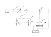
<光学系の構成>
最初に、図1を参照して、光干渉装置の構成を大まかに説明する。光源101から出射した計測光がレンズ102、ビームスプリッタ103、XYスキャナ104、対物レンズ105を介して観察対象である半導体などの試料106に到達する。試料表面には透過性の膜が配置されており、それらの表面および界面で反射された光は、対物レンズ105、XYスキャナ104、ビームスプリッタ103、結像レンズ107を介して、分光器108に到達する。
<Configuration of optical system>
First, the configuration of the optical interference apparatus will be roughly described with reference to FIG. The measurement light emitted from the
光源101にはハロゲンランプなどが用いられ、波長は例えば400−800nmである。ここで、分光器108としては、回折格子型分光器を用いる。この場合、分光器108は、回折格子109および撮像素子110などで構成される。回折格子109によって分光された光は分光器内部の撮像素子110によって波長のスペクトルデータとして取得される。撮像素子110はCCD型ラインセンサーなどである。なお、回折格子型分光器を採用する利点としては、種類が豊富、使用波長領域で分散がほぼ一定などが挙げられる。一方、短所としては、透過率が低い、迷光が多い、次数の重複が起こる、出射光の偏光度が多いなどが挙げられる。
A halogen lamp or the like is used as the
撮像素子で撮像されたスペクトルデータはコンピューター111で解析される。当然コンピューター111は解析を行うだけでなく、データの記憶、画像の表示、測定の指令を出す機能を有している。また、コンピューター制御によりXYスキャナで計測光を試料に対して光軸に垂直な方向にラスタースキャンし、試料の断面像を得ることができる。コンピューター111は、CPUおよびメモリーなどから構成され、CPUがプログラムを実行することで上記の各機能を実現する。ただし、上記の各機能の一部または全部をハードウェアによって実現しても構わない。
Spectral data captured by the image sensor is analyzed by the
<干渉条件>
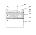
図2を用いて多層構造の干渉条件について説明する。なお、簡単のため多重反射の影響は考慮しない。
<Interference conditions>
The interference condition of the multilayer structure will be described with reference to FIG. For simplicity, the influence of multiple reflection is not considered.
多層構造の試料は、屈折率Nsの基板204の上に、屈折率N2の第2の膜203、屈折率N1の第1の膜202が設けられた構成である。この試料は、屈折率N0の媒質に配置されているとする。それぞれの境界は表面205、第1の界面206、第2の界面207となっている。それらの空間距離はD1およびD2である。ここで、互いに接する媒質の屈折率は異なるものとする。
Samples of multi-layer structure, on a
なお、光が屈折率の低い媒質から屈折率の高い媒質へ入射するとき、界面で反射した光の位相は変化しない。しかしながら、光が屈折率の高い媒質から屈折率の低い媒質へ入射するとき、界面で反射した光の位相はπ変化する。ここでは、屈折率はN0<N1<N2<Nsの関係を満たしている試料を計測する場合を考える。例えば、それぞれ空気:N0=1、レジスト:N1=1.5、シリコンナイトライド:N2=2.0、シリコン基板:Ns=3.5、である。この条件では、反射の前後で計測光201の位相は変化しない。
Note that when light enters a medium having a low refractive index from a medium having a low refractive index, the phase of the light reflected at the interface does not change. However, when light enters from a medium having a high refractive index to a medium having a low refractive index, the phase of the light reflected at the interface changes by π. Here, a case is considered where a sample whose refractive index satisfies a relationship of N 0 <N 1 <N 2 <N s is measured. For example, air: N 0 = 1, resist: N 1 = 1.5, silicon nitride: N 2 = 2.0, and silicon substrate: N s = 3.5, respectively. Under this condition, the phase of the
従って、ある膜の両側の界面で反射した光が干渉する条件は、その膜の屈折率n、界面間の空間距離d、整数(干渉次数)m、波数kを用いると、強めあう条件として数式1のように表される。 Therefore, the conditions under which light reflected at the interfaces on both sides of a film interferes with each other are expressed as a condition for strengthening using the refractive index n of the film, the spatial distance d between the interfaces, an integer (interference order) m, and the wave number k. It is expressed as 1.

また、弱めあう条件として数式2のように表される。
当然、膜の構成は様々であり、反射の前後で位相の変化がある屈折率の組み合わせではそれを考慮する必要がある。その結果、強めあう条件と弱めあう条件が数式1、2で逆になることがある。
Naturally, there are various film configurations, and it is necessary to consider the combination of refractive indexes having a phase change before and after reflection. As a result, the conditions for strengthening and the conditions for weakening may be reversed in
<信号処理>
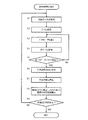
本発明の信号処理工程について、図3A〜Dを用いて説明する。ここでは図2に示す構成の膜を測定する場合を例にとって説明する。なお、以下の各処理はコンピューター111によって実行されるものである。
<Signal processing>
The signal processing step of the present invention will be described with reference to FIGS. Here, a case where a film having the structure shown in FIG. 2 is measured will be described as an example. The following processes are executed by the
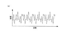
S1の工程において、分光器108からのスペクトルデータを取得する。このときのデータが図3Bに模式的に示されている。図3Bは縦軸が強度で横軸が波数である。なお、通常の分光器のスペクトルは波長に対する強度であることが多い。ここでは波数スペクトルを利用するので、そのような場合には、波長をその逆数である波数に変換する必要がある。さらに、波長スペクトルは波長に対して等間隔なデータとなっているため、逆数である波数に変換したときに変換後のデータは波数に対して等間隔とならない。そのため、補間処理などにより、波数スペクトルとして等間隔にすることが必要となる。
In the step S1, spectrum data from the
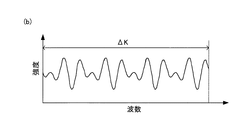
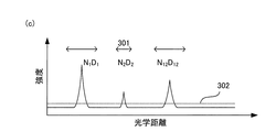
S2の工程(本発明の第1の工程に相当)において、スペクトルデータのフーリエ変換を行う。ここでラインセンサーのサンプリング数は有限であるため離散フーリエ変換となる。一般にはサンプリング数(ラインセンサーの画素数)Nとして512、1024、2048などが選択される。このときの結果が図3Cに模式的に示されている。離散フーリエ変換をした場合の横軸は光学距離に比例した値(光学距離に対応した情報)となる。この値から光学距離を算出可能である。なお、離散フーリエ変換から得られる結果は光学距離に比例した値であるが、記述の簡略化のため、以下では、離散フーリエ変換の結果として光学距離が得られると記述する。この光学距離の横軸は、ラインセンサーのサンプリング数で分割されている。 In step S2 (corresponding to the first step of the present invention), Fourier transform of the spectrum data is performed. Here, since the sampling number of the line sensor is finite, discrete Fourier transform is performed. Generally, 512, 1024, 2048 or the like is selected as the sampling number (number of pixels of the line sensor) N. The result at this time is schematically shown in FIG. 3C. When the discrete Fourier transform is performed, the horizontal axis is a value proportional to the optical distance (information corresponding to the optical distance). The optical distance can be calculated from this value. Note that the result obtained from the discrete Fourier transform is a value proportional to the optical distance, but for the sake of simplicity of description, it will be described below that the optical distance is obtained as a result of the discrete Fourier transform. The horizontal axis of this optical distance is divided by the number of samplings of the line sensor.
図3Cに示すように、ここでは、N1D1,N2D2およびN12D12のピークが計測される。当然これらの値をもって各膜の光学距離とすることができる。しかしながら、離散フーリエ変換では計測結果が離散的な値となる。すなわち、光学距離の計測結果は、整数i、図3Bに示す分光器の帯域幅ΔKを用いて数式3のように表される。なお、iは0≦i≦N/2を満足する整数である。また、λmax、λminはそれぞれ分光器の検出最大波長と最小波長である。
As shown in FIG. 3C, here, peaks of N 1 D 1 , N 2 D 2 and N 12 D 12 are measured. Naturally, these values can be used as the optical distance of each film. However, in the discrete Fourier transform, the measurement result becomes a discrete value. That is, the measurement result of the optical distance is expressed as
膜厚の計測分解能δ(nd)は計測結果としてとりうる光学距離の最小間隔であるので、数式4のように表される。なお、この式は、計測できる最小の距離ndminでもある。
また、計測できる最大の距離ndmaxは数式3のiにN/2を代入して数式5のように得られる。これは、サンプリング定理によって決まる。
ところで、多層構造でi番目の層からt番目の層の両端で干渉する場合、数式6に示すように、i〜t番目の層の光学距離NitDitは、i〜t−1番目の層の光学距離Nit−1Dit−1と、t番目の層の光学距離NtDtとの和になる。これを順次繰り返していけば、i〜t番目の層(全体)の光学距離NitDitは、i番目の層からt番目の層までの各層の光学距離の和と一致する。 By the way, when interference occurs at both ends of the t-th layer from the i-th layer in the multi-layer structure, the optical distance N it D it of the i-t-th layer is i-t-1th as shown in Equation 6. This is the sum of the optical distance N it-1 D it-1 of the layer and the optical distance N t D t of the t-th layer. If this is repeated in sequence, the optical distance N it D it of the i to t th layer (whole) coincides with the sum of the optical distances of the respective layers from the i th layer to the t th layer.
![]()
![]()
当然、これらの値は、フーリエ変換した後にピークとして出てくる。n層あるときのピークの数はn+1から2層を選ぶ組み合わせ数となる。例えば、図2に示すような2層構成の膜からは、図3Cに示すように3つのピークが得られる。 Naturally, these values appear as peaks after Fourier transform. The number of peaks when there are n layers is the number of combinations for selecting two layers from n + 1. For example, from a film having a two-layer structure as shown in FIG. 2, three peaks are obtained as shown in FIG. 3C.
S3の工程(本発明の第2の工程に相当)において、フーリエ変換の結果にフィルターをかけて、1つのピークに対応する光学距離を選択する。このようなフィルターとしてはバンドパスフィルターがある。なお、ここでのバンドは物理量で言うと長さに相当する単位を持つ。デジタルデータで考えた場合は、単位に無関係で処理は同じなので便宜的にこのように呼ぶ。さらに、デジタルで処理しているためピクセル数に変換係数を乗じた値がバンド幅であり、ここでは、ピクセル数をバンド幅と呼んで議論することもある。従って、一般的な周波数や波長の幅とは異なっていることに注意されたい。フィルターのバンド
幅301は図3Cに示されるように、N1D1,N2D2およびN12D12のピークに応じて設定する。ちなみに、これらの光学距離はS7の工程で再度呼び出せるようにメモリーなどに格納する。
In step S3 (corresponding to the second step of the present invention), the result of the Fourier transform is filtered to select an optical distance corresponding to one peak. Such a filter includes a band pass filter. Note that the band here has a unit corresponding to the length in terms of physical quantity. In the case of digital data, the processing is the same regardless of the unit, so it is called as such for convenience. Further, since digital processing is performed, a value obtained by multiplying the number of pixels by a conversion coefficient is a bandwidth, and here, the number of pixels is sometimes called a bandwidth. Therefore, it should be noted that it is different from general frequency and wavelength width. The
フィルターに設定するバンド幅(抽出範囲)は、例えば、ピークが閾値302以上である範囲などとすることができる。また、各領域が互いに重ならないようにバンド幅を設定することが望ましい。また、バンド幅が広くなるほど所望の光学距離と異なる成分を含むため必要最低限でよい。例えば、閾値と接触する幅の倍の幅をバンド幅として設定する。当然、N2D2のピークのように強度が小さい場合に対応できるように、バンド幅を可変にすることが好ましい。なお、おおよその層構成が分かっている場合は、バンド幅を固定してもよい。
The bandwidth (extraction range) set in the filter can be, for example, a range where the peak is equal to or greater than the
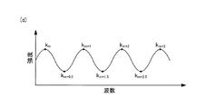
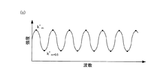
S4の工程(本発明の第3の工程に相当)においては、フィルター後の信号に逆離散フーリエ変換を行う。図3Dにその波形が模式的に示されている。光学距離に対してピークが一つであることから単層の結果に対応したほぼ正弦波となる。すなわち極大値と極小値が繰り返すような波形が得られる。 In step S4 (corresponding to the third step of the present invention), an inverse discrete Fourier transform is performed on the filtered signal. The waveform is schematically shown in FIG. 3D. Since there is one peak with respect to the optical distance, it becomes a substantially sine wave corresponding to the result of the single layer. That is, a waveform in which the maximum value and the minimum value repeat is obtained.
S5の工程で必要なピークの数に対して、逆フーリエ変換が行われたかどうかが判定される。終わっていない場合は次のピークのデータについて逆フーリエ変換を行う。この例では3回逆フーリエ変換を行う。 It is determined whether the inverse Fourier transform has been performed on the number of peaks required in the step S5. If not, the inverse Fourier transform is performed on the next peak data. In this example, the inverse Fourier transform is performed three times.
S6の工程(本発明の第4の工程に相当)において、正弦波の極大値または極小値に対応する波数を抽出する。ここでは、図3Dのように、強めあう条件に対応する波数がkmを含めて4つ、弱めあう条件に対応する波数がkm+0.5を含めて3つ得られる。 In step S6 (corresponding to the fourth step of the present invention), the wave number corresponding to the maximum value or the minimum value of the sine wave is extracted. Here, as in FIG. 3D, the wave number corresponding to the constructive condition is four including k m, the wave number corresponding to the destructive condition can be obtained three including k m + 0.5.
S7の工程(本発明の第5の工程に相当)において、干渉次数を計算する。干渉が強めあう条件式(ここでは数式1)に、S3の工程で抽出したピークの光学距離、S6の工程で抽出した極大値の波数を代入することによって、干渉条件における干渉次数mを計算する。2つの反射波の光路差(層厚の光学距離の2倍)の、図3Dで極大をとる波数(に対応する波長)に対する比を計算する。このときの波数は、例えば、複数ある極大値のうち最も小さいものを選んでも良いし、波形の安定しているピークでの波数を選んでもよい。なお、ここでは極大値での波数と強めあう条件式を利用してmを求めているが、極小値での波数と弱めあう条件式を利用してmを求めても良い。 In step S7 (corresponding to the fifth step of the present invention), the interference order is calculated. The interference order m in the interference condition is calculated by substituting the peak optical distance extracted in the step S3 and the wave number of the maximum value extracted in the step S6 into the conditional expression (here, the mathematical expression 1) that strengthens the interference. . The ratio of the optical path difference between the two reflected waves (twice the optical distance of the layer thickness) to the wave number (corresponding to the wavelength) that takes the maximum in FIG. 3D is calculated. As the wave number at this time, for example, the smallest one among a plurality of maximum values may be selected, or the wave number at a stable peak of the waveform may be selected. Here, m is obtained using a conditional expression that strengthens the wave number at the maximum value, but m may be obtained using a conditional expression that weakens the wave number at the minimum value.
ところで、S7の工程で用いる各層の光学距離は、S6の工程の結果から算出することも可能である。つまり、図3Dにおける2つのピークにおける波数kmとkm+lを使って計算してもよい。ここで、lは図3Dでmからl番目であることを示す。kmとkm+lをそれぞれ数式1に代入した2つの式からmを消去することによって、数式7に示すように各層の光学距離を得ることができる。このように逆フーリエ変換後の波数スペクトルからピークをとる波数を複数求めることによっても、各層の光学距離を算出することができ、この値をS7の工程で利用しても良い。
By the way, the optical distance of each layer used in the process of S7 can be calculated from the result of the process of S6. That may be calculated using the wavenumber k m and k m + l at two peaks in Figure 3D. Here, l indicates that it is l-th from m in FIG. 3D. The k m and k m + l from two equations obtained by substituting the
通常、多層構造を解析する場合は各層の屈折率が分かっているためS6の工程で数式1、数式2のどちらを使うか予め決めることができる。しかしながら、各層の屈折率が分か
っていないような場合にはどちらの数式を用いればよいのか分からない。このような場合には、数式1および数式2を用いて、mをそれぞれ計算する。その後、km+1、km+2、・・・において光学距離ndを計算する。ndの誤差が最小になる方を選択することによって、mを決定することができる。また、これによって層間の屈折率の大小関係を知ることができる。
Normally, when analyzing a multilayer structure, since the refractive index of each layer is known, it is possible to determine in advance whether to use
S8の工程(本発明の第6の工程に相当)では、S7の工程で求めたmを整数Mmに四捨五入し、再度強めあう条件または弱めあう条件を使って光学距離を再計算する。本来、干渉が強めあう条件では、光路差は波長の整数倍になる。S7の工程で求めたmが整数にならない場合には、それは誤差に起因するものである。そこで、求められたmを最も近い整数Mmに近似(補正)することで、mに含まれる誤差を排除することができる。S7の工程において強めあう条件を利用した場合では、数式8を使って光学距離を算出する。 In S8 of step (corresponding to the sixth step of the present invention), rounded to m obtained in the step of S7 to an integer M m, it recalculates the optical distance with the condition or destructive conditions constructive again. Originally, under the condition that interference increases, the optical path difference becomes an integral multiple of the wavelength. If m obtained in step S7 is not an integer, it is due to an error. Therefore, to approximate to the nearest integer M m the obtained m (corrected), it is possible to eliminate the error contained to m. When the strengthening condition is used in the process of S7, the optical distance is calculated using Equation 8.
一方、干渉が弱めあう条件では、光路差は波長の半整数倍となるはずである。S7の工程において弱めあう条件を利用した場合は、数式9によって光学距離を算出する。
S9の工程では、計測が所望の領域で終了したかどうかを判断する。終了していない場合は、次の領域で計測を行う。この工程を繰り返し、所望の回数を終了すれば、図2に対応した断層像を得ることができる。 In step S9, it is determined whether the measurement has been completed in a desired area. If not completed, measure in the next area. If this process is repeated and the desired number of times is completed, a tomographic image corresponding to FIG. 2 can be obtained.
なお、断層像の深さ方向はサンプリング数Nで区切られている。本方式では、サンプリング数以下の計測を行っている。従って、この計算結果を反映した断層像を構成する必要がある。また、新たな断層像を構成しない場合であっても、計測した数値を補助的に表示してもよい。 The depth direction of the tomographic image is divided by the sampling number N. In this method, the number of samplings or less is measured. Therefore, it is necessary to construct a tomographic image reflecting this calculation result. Even if a new tomographic image is not formed, the measured numerical values may be displayed supplementarily.
<数値例>
ここで簡単に数値を使って説明する。作製した試料が設計どおりの構成になっているかを計測したい場合を想定する。すなわち、試料が設計値から大きくずれていないような状況である。
<Numerical example>
Here is a simple explanation using numerical values. Assume a case in which it is desired to measure whether the fabricated sample has the structure as designed. That is, the sample is not greatly deviated from the design value.
計測系は、ハロゲンランプの400nm−800nmのスペクトルを全て使うこととする。このとき、計測できる最小距離ndminおよび計測分解能は数式4より400nm(0.4μm)である。なお、分光器108の帯域幅ΔKは1.25×10⁶[m−1](=1/400nm−1/800nm)である。また、分光器108のサンプリング数がN=1024の場合、計測できる最大距離ndmaxは数式5から205μmとなる。
The measurement system uses all the 400 nm-800 nm spectrum of the halogen lamp. At this time, the minimum measurable distance nd min and the measurement resolution are 400 nm (0.4 μm) according to Equation 4. The bandwidth ΔK of the
試料はD1=5μm、D2=10μm程度であり、N1=1.5、N2=2の層がSi基板上:Ns=3.5に配置されているとする。光学距離はそれぞれ、おおよそ、N1D1=7.5μm、N2D2=20μm、N12D12=27.5μmであり、フーリエ変
換(図3AのS2)の結果としてこの付近にピークが発生することになる。
It is assumed that the sample has D 1 = 5 μm and D 2 = 10 μm, and a layer of N 1 = 1.5 and N 2 = 2 is arranged on the Si substrate: N s = 3.5. The optical distances are approximately N 1 D 1 = 7.5 μm, N 2 D 2 = 20 μm, and N 12 D 12 = 27.5 μm, respectively. As a result of Fourier transform (S2 in FIG. 3A), a peak appears in this vicinity. Will occur.
サンプリング数N(ここでは1024)のデータを離散フーリエ変換をした場合、横軸はN個に分割される。ただし、N/2(=512)を境に対称となるため、片側で議論する。まず、S2の工程で、512分割された横軸のうち、1ピクセルあたり、最小距離(0.4μm)であるので、19(≒7.5/0.4)、50(≒20/0.4)、69(
≒27.5/0.4)のピクセル付近にピークが発生することになる。ピークの間隔がそれぞれ離れていることから、S3の工程で3つの帯域にバンドパスフィルターを設定してこれらのピークを分離することができる。S4の工程で逆離散フーリエ変換をする。まず、層厚の光学距離が7.5μmである場合、強めあう条件として、m=19(λ=789.4nm)〜37(λ=405.5nm)のピークが400nm〜800nmの範囲に現
れる。また、層厚の光学距離が20μmである場合、強めあう条件として、m=50(λ=800nm)〜100(λ=400nm)のピークが現れる。ただし、両端はピークであることが判別できないため、実際には51〜99になる。
When the data of sampling number N (here, 1024) is subjected to discrete Fourier transform, the horizontal axis is divided into N pieces. However, since it becomes symmetrical with N / 2 (= 512) as a boundary, it will be discussed on one side. First, in the step S2, the minimum distance (0.4 μm) per pixel of the 512 divided horizontal axes is 19 (≈7.5 / 0.4), 50 (≈20 / 0. 4), 69 (
A peak occurs in the vicinity of the pixel of ≈27.5 / 0.4). Since the peak intervals are separated from each other, band peaks can be set in the three bands in step S3 to separate these peaks. Inverse discrete Fourier transform is performed in step S4. First, when the optical distance of the layer thickness is 7.5 μm, as a strengthening condition, a peak of m = 19 (λ = 789.4 nm) to 37 (λ = 405.5 nm) appears in a range of 400 nm to 800 nm. When the optical distance of the layer thickness is 20 μm, a peak of m = 50 (λ = 800 nm) to 100 (λ = 400 nm) appears as a strengthening condition. However, since it cannot be determined that both ends are peaks, the actual values are 51 to 99.
ここで層厚の光学距離が約7.5μmの場合について、さらに述べる。S2の工程におけるフーリエ変換の結果(ピークが19ピクセル目)から、この層の光学距離として7.6μm(0.4×19)が得られる。その前後の値は、7.2μm、8.0μmとなり、0.4μm刻みでしか計測できない。一方、S7の工程において、最も小さい極大値の波数が2.466×10⁶(λ=405.5nm)であったとする。これらの値を、強めあう干渉条件を表す数式1に代入することで、m=37.03が得られる。このmを整数近似するとM=37となる。そして、このようにして求めたMをS8の工程で数式8に代入することで、層の光学距離を7.502μm(=37/(2×2.466×106))とより精度良く求めることが可能となる。
Here, the case where the optical distance of the layer thickness is about 7.5 μm will be further described. From the result of Fourier transform in the step of S2 (peak is the 19th pixel), 7.6 μm (0.4 × 19) is obtained as the optical distance of this layer. The values before and after that are 7.2 μm and 8.0 μm, and can only be measured in increments of 0.4 μm. On the other hand, it is assumed that the wave number of the smallest maximum value is 2.466 × 10 6 (λ = 405.5 nm) in the process of S7. By substituting these values into
ここで、計測精度について述べる。なお、計測精度は、各層の分離後の位置決め精度のことを指し、計測分解能は各層を分離できる空間距離とする。分光器108は400nmの帯域を1024画素で分割していることから、分光器108のスペクトル分解能は0.39nmである。mについての誤差は除去できるので、計測精度は理論的に数式10で表される。m≒100となる上記の条件では、計測精度は20nm程度となる。当然、mが小さい方が計測精度がよくなる。
Here, the measurement accuracy will be described. Note that the measurement accuracy refers to the positioning accuracy after separation of each layer, and the measurement resolution is a spatial distance at which each layer can be separated. Since the
一方、離散フーリエ変換のみによって光学距離を計測する場合、計測精度と計測分解能は同じで数式4より400nmとなる。 On the other hand, when the optical distance is measured only by the discrete Fourier transform, the measurement accuracy and the measurement resolution are the same, and 400 nm from Equation 4.
このように、本発明による計測方法によると計測精度が大幅に向上することになる。つまり、離散フーリエ変換のみで多層構造の光学距離を計算する従来の方法は、数式3で示される光学距離しか表現できないため離散的な値となる。実際の値が離散した数値の間にある場合、その周辺にデータが分散するいわゆるスペクトルのリークが起こる(図3Cの例でいうと、ピークが鈍った波形になる)。そして、その分解能は光源の帯域幅(波数の幅ΔK)によって定まる。一方、本方式ではバンドパスフィルターで複数のデータを切り出し、逆離散フーリエ変換をして、一層分のほぼ正弦波の波数スペクトルを構成することができる。つまり、リークしたスペクトルを集めて波形を再構成する。この場合、分光器の帯域幅ΔKに、周期が整数以外の正弦波を表現できることを意味している。ただし、バ
ンド幅が最小分解能(1ピクセル)のときは離散フーリエ変換の結果と一致することになる。なぜなら、周辺にリークしたデータを活用できないからである。従って、離散フーリエ変換で十分なバンド幅で分離できるときに本発明の方式は有効な手法となる。また、屈折率が波長に依存するような場合は波長に対応した屈折率を用いることができるのでさらに高精度な計測が可能となる。
Thus, according to the measurement method of the present invention, the measurement accuracy is greatly improved. That is, the conventional method of calculating the optical distance of the multilayer structure only by the discrete Fourier transform can express only the optical distance represented by
なお、層の構成が計測条件に合わないような場合も当然ありうる。例えば、多層構造の各層は数式3で表現できる条件を満たしていても、それらを足し合わせた状態がndmaxを超えるような場合である。このような場合でも、そのような成分が測定ノイズとして分光器に加わるが、本手法が全く使えないわけではない。
Of course, there may be cases where the layer configuration does not meet the measurement conditions. For example, even when each layer of the multilayer structure satisfies the condition that can be expressed by
また、光源として波長を掃引できるようなスイープ光源を用いる場合は検出器としてフォトダイオードを使い、オペアンプなどによって増幅した後、AD変換機でPCに取り込む。このような方式の場合であっても本方式を使うことは可能である。 When a sweep light source capable of sweeping the wavelength is used as a light source, a photodiode is used as a detector, amplified by an operational amplifier or the like, and then taken into a PC by an AD converter. Even in such a system, it is possible to use this system.
[第2の実施形態]
第2の実施形態においては、参照ミラーを使う構成の光干渉装置について図面を用いて説明する。ここでは、主に第1の実施形態との相違点を説明する。
[Second Embodiment]
In the second embodiment, an optical interference device configured to use a reference mirror will be described with reference to the drawings. Here, differences from the first embodiment will be mainly described.
<光学系の構成>
まず、図4を用いて光干渉装置の装置構成について説明する。光源101から出射した光がビームスプリッタ103によって参照光404と測定光112とに分割される。測定光は、観察対象である試料106によって反射され、戻り光113となって戻される。一方、参照光は参照ミラー401によって反射される。なお、参照ミラー401は位置調整機構402によって光路長を調整することができる。参照光はビームスプリッタ103によって、戻り光と合波される。このように、本実施形態における光干渉装置の光学系は、光源からの光を、測定光と参照光に分割し、測定光を試料106に導きその戻り光を検出位置に導くとともに、参照光路を介して参照光を検出位置に導くものである。
<Configuration of optical system>
First, the apparatus configuration of the optical interference apparatus will be described with reference to FIG. Light emitted from the
合波された光は、結像レンズ107を介して分光器403に到達する。ここでは分光器403に、プリズム405を用いる。プリズムには、透過率が高い、迷光が少ない、次数重複がない、出射光の偏光度が小さいなどの長所がある。一方短所として、材料に制限がある、分散の波長依存性があるなどがある。
The combined light reaches the
ここで、参照ミラー401を使用する理由について説明する。まず、試料からの戻り光は、試料表面、第1の界面、第2の界面などで反射する光である。この戻り光の波数kでの電界をEs(k)とする。また、参照ミラーでの反射光(参照光)の波数kでの電界をEr(k)とする。このとき、分光されて撮像素子110に入ってくる波数kの光強度P(k)は、複素共役を示す記号*を用いて、数式11のような関係になる。
Here, the reason for using the
参照ミラー401を使わない場合には、撮像素子に入射する光の強度は、右辺第4項のみになる。試料の反射率が低い場合には十分な光強度を得ることができず、ノイズに埋もれて検出できなくなってしまう。
When the
一方、参照ミラー401を使用する場合は、数式11の全ての項が入射光の強度に寄与する。このうち、試料106からの戻り光と参照ミラー401からの参照光との干渉に関わる成分は右辺の第2および第3項である。この成分は、Esが小さい場合には小さくなる。網膜のような多層構造は互いの屈折率差が小さいため界面での反射率が低く、Esが小さくなる。このような場合であっても、参照光の光量を大きくすることで、撮像素子に入射する光強度を上げることができる。
On the other hand, when the
また、参照ミラーを使わない場合、各層の相対的な位置関係が分からなくなる、各層を分離できないなどの問題が発生する。これらの理由により、光学系の構成が複雑になるが参照ミラーを用いる方式が使われることがある。 In addition, when the reference mirror is not used, there arise problems that the relative positional relationship between the layers is not understood and the layers cannot be separated. For these reasons, the configuration of the optical system is complicated, but a method using a reference mirror may be used.
<参照ミラーに対する光学距離>
次に、図5を用いて多層構造の構成ついて説明する。なお、簡単のため多重反射の影響は考慮しない。また、参照ミラー501は等価的に試料と同軸上にあるとしてよいので図のような配置とする。ここで、戻り光と参照光の光路差は、参照ミラーから試料表面までの距離をL0として表される。また、参照ミラーから第1の界面および参照ミラーから第2の界面までの光学距離をそれぞれNm1L1、Nm2L2とする。なお、多層構造の試料は屈折率Nsの基板204の上に屈折率N2の第2の層203、屈折率N1の第1の層202の構成で、屈折率N0の媒質に配置されているとする。各層の空間距離はD1およびD2である。
<Optical distance to the reference mirror>
Next, the configuration of the multilayer structure will be described with reference to FIG. For simplicity, the influence of multiple reflection is not considered. Further, since the
<信号処理>
本実施形態における信号処理工程のうち、第1の実施形態との差異について、図5の構成を例に説明する。S1の工程において、分光器からのスペクトルデータを取得する。このときのデータが図6Aに模式的に示されている。
<Signal processing>
Of the signal processing steps in the present embodiment, differences from the first embodiment will be described by taking the configuration of FIG. 5 as an example. In the step S1, spectrum data from the spectroscope is acquired. The data at this time is schematically shown in FIG. 6A.
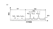
S3の工程において、フーリエ変換の結果にフィルターをかける。まず、フーリエ変換の結果は図6Bに示すようになり、光学距離がそれぞれN0L0、Nm1L1、Nm2L2の位置にピークが現れる。これらの光学距離は、それぞれ参照ミラー501と試料表面205、第1の界面206、第2の界面207の光学距離に対応する。同時に、第1の実施形態と同様に多層構造自身の干渉によるN1D1,N2D2およびN12D12にもピークが現れる。
In step S3, the result of Fourier transform is filtered. First, the result of the Fourier transform is as shown in FIG. 6B, and peaks appear at positions where the optical distances are N 0 L 0 , N m1 L 1 , and N m2 L 2 , respectively. These optical distances correspond to the optical distances of the
なお、参照ミラー501を、このミラー501と試料表面205との光学距離N0L0が多層構造全体の厚さN12D12より長くなるように設定することが好適である。これにより、試料自身での干渉成分が現れる第1の領域601と、試料と参照ミラーの干渉成分が現れる第2の領域602とを分離することができる。
The
上記の結果得られたピークの1つをフィルターによって選択した後は、上記の第1の実施形態と同様の手法で光学距離を計算する。つまり、S4の工程で逆フーリエ変換することで図6Cに示す結果が得られる。 After one of the peaks obtained as a result of the above is selected by the filter, the optical distance is calculated by the same method as in the first embodiment. That is, the result shown in FIG. 6C is obtained by performing the inverse Fourier transform in step S4.
そして、S6の工程(本発明の第7の工程に相当)で、図6Cの結果から波数を特定して干渉条件の数式1から、干渉次数mを算出する。S7の工程では、求めたmを整数に四捨五入し、これを干渉条件の数式に代入して光学距離を計算する。
In step S6 (corresponding to the seventh step of the present invention), the wave number is specified from the result of FIG. 6C, and the interference order m is calculated from
なお、参照ミラーを用いる場合、各層の距離は次のような関係である。
![]()
![]()
従って、1層目の空間距離は数式13のようになる。
同様に、2層目の空間距離は数式14のようになる。
これをi+1層目の場合に拡張すると次のようになる。
この空間距離を画像化すれば、図5に基づいた空間距離の断層像を得ることができる。なお、従来の断層像は光学距離の断層像である。 If this spatial distance is imaged, a tomographic image of the spatial distance based on FIG. 5 can be obtained. Note that a conventional tomographic image is a tomographic image of an optical distance.
[第3の実施形態]
第3の実施形態においては、本発明を適用した眼科用OCT装置の光学系について図7を用いて詳しく説明する。基本的な構成は、第2の実施形態の参照ミラーを使うタイプである。
[Third Embodiment]
In the third embodiment, an optical system of an ophthalmic OCT apparatus to which the present invention is applied will be described in detail with reference to FIG. The basic configuration is a type that uses the reference mirror of the second embodiment.
<光学系の構成>
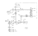
図7は、全体としてマッハツェンダー干渉系を構成している。光源701から出射した光がビームスプリッタ703−1によって参照光705と測定光706とに分割される。測定光706は、観察対象である眼707によって反射や散乱により戻り光708となって戻された後、ビームスプリッタ703−2によって、参照光705と合波され、分光器721に入射する。
<Configuration of optical system>
FIG. 7 constitutes a Mach-Zehnder interference system as a whole. Light emitted from the
まず、光源701の周辺について説明する。光源701は代表的な低コヒーレント光源であるSLD(Super Luminescent Diode)である。波長は830nm、バンド幅50nmである。ここで、バンド幅は、得られる断層像の光軸方向の分解能に影響するため、重要なパラメーターである。また、光源の種類は、ここではSLDを選択したが、低コヒーレント光が出射できればよく、ASE(Amplified Spontaneous Emission)等も用いることができる。また、波長は眼を測定することを鑑みると、近赤外光が適する。さらに波長は、得られる断層像の横方向の分解能に影響するため、なるべく短波長であることが望ましく、ここでは830nmとする。観察対象の測定部位によっては、他の波長を選んでももちろん良い。光源701から出射された光はシングルモードファイバー710−1を通して、レンズ711−1に導か
れる。
First, the periphery of the
次に、参照光705の光路について説明する。ビームスプリッタ703−1によって分割された参照光705はミラー714−1〜3に連続して入射され、方向を変えることで、ビームスプリッタ703−2により分光器721に入射される。ここで、715−1〜2は分散補償用ガラスである。分散補償用ガラス715−1は眼707に測定光706が往復したときの分散を、参照光705に対して補償するものである。つまり、分散補償用ガラス715−1の長さL1は、一般的な眼の奥行きの2倍と等しいことが望ましい。ここでは、日本人の平均的な眼球の直径とされる23mmの2倍のL1=46mmとする。さらに、電動ステージ717は、矢印で図示している方向に移動することができ、参照光705の光路長を、調整・制御することができる。分散補償用ガラス715−2は眼707のスキャンに用いられるレンズ720−1,2の分散補償を目的としたものである。
Next, the optical path of the
測定光706の光路について説明する。ビームスプリッタ703−1によって分割された測定光706は、分散補償用ガラス715−3を通り、ビームスプリッタ703−3で反射される。次に、XYスキャナ719のミラーに入射される。XYスキャナ719は、網膜723上を光軸に垂直な方向にラスタースキャンするものである。また、測定光706の中心はXYスキャナ719のミラーの回転中心と一致するように調整されている。レンズ720−1,2は網膜723を走査するための光学系であり、測定光706を角膜722の付近を支点として、網膜723をスキャンする役割がある。ここでは、レンズ720−1,2の焦点距離はそれぞれ50mm、50mmである。測定光706は眼707に入射すると、網膜723からの反射や散乱により戻り光708となる。さらに、戻り光708はビームスプリッタ703−3によって戻り光708−1と708−2とに分割され、その一方である戻り光708−1は、分光器721に導かれる。また、もう一方の戻り光708−2はビームスプリッタ703−1を透過され、検出器724に導かれる。検出器は、干渉信号と同様に、電気的にコンピューター725に取り入れられ、戻り光708−2の強度を記録および表示とを行うことができる。また、検出器724で得られる信号は、網膜723での反射や散乱による戻り光708−2の強度信号であり、深さ分解能を持たない。検出器724は、例えば高速・高感度な光センサであるAPD(Avalanche Photo Diode)が用いられる。
The optical path of the
<数値例>
ここで、数値を使って説明する。対象物は目であり、その物理的大きさおよび構造は人によって大きく変わらない。ただし、ここでは簡単のため次のような構造とする。まず、網膜全体の空間距離を560μmとし、7層で構成され、各層の空間距離が80μmとする。また、屈折率を1.5(各層の屈折率は異なっていないと界面で反射しないがここでは簡単な数値計算をするため全て同じとする)とする。従って、各層の光学距離は120μmで、全体の光学距離は840μmとなる。ミラーの位置は、空間距離でL0=400μmとなるような位置とし、光学距離は600μmとなる。
<Numerical example>
Here, it explains using numerical values. The object is the eye, and its physical size and structure does not vary greatly from person to person. However, for simplicity, the following structure is used. First, the spatial distance of the entire retina is set to 560 μm, it is composed of seven layers, and the spatial distance of each layer is set to 80 μm. Further, the refractive index is set to 1.5 (if the refractive index of each layer is not different, it is not reflected at the interface, but here all are the same for simple numerical calculation). Therefore, the optical distance of each layer is 120 μm, and the total optical distance is 840 μm. The position of the mirror is such that the spatial distance is L 0 = 400 μm, and the optical distance is 600 μm.
805nm−855nmのスペクトルを全て使う場合には、計測できる最小の距離ndminは6.9μmである。また、N=1024の場合、計測できる最大の距離ndmaxは3.5mm(光学距離)となる。干渉スペクトルを離散フーリエ変換すれば、1ピクセルあたり6.9μmなので、87、104、122、139、157、174、191、209ピクセル付近にピークが立つ。これらのピークが離れていることから分離することが可能である。光学距離が最短の600μmであるとき、強めあう条件はm=1404〜1490、光学距離が最長の1440μmのとき強めあう条件は、m=3369〜3577である。一方、50nmを1024分割しているため、分光器の分解能は0.049nmである。計算する波長によって条件は変わるが、m=4000で計測精度は理論的に100nm程度ということになる。離散フーリエ変換の計測精度が6.9μmであるから
大幅に改善するということが言える。
When the entire spectrum of 805 nm to 855 nm is used, the minimum distance nd min that can be measured is 6.9 μm. When N = 1024, the maximum distance nd max that can be measured is 3.5 mm (optical distance). If the interference spectrum is subjected to discrete Fourier transform, it is 6.9 μm per pixel, so that peaks appear in the vicinity of 87, 104, 122, 139, 157, 174, 191 and 209 pixels. It is possible to separate these peaks from their separation. When the optical distance is the shortest 600 μm, the conditions for strengthening are m = 1404 to 1490, and when the optical distance is the longest 1440 μm, the conditions for strengthening are m = 3369 to 3577. On the other hand, since 50 nm is divided into 1024, the resolution of the spectroscope is 0.049 nm. Although the conditions vary depending on the wavelength to be calculated, the measurement accuracy is theoretically about 100 nm when m = 4000. Since the measurement accuracy of the discrete Fourier transform is 6.9 μm, it can be said that it is greatly improved.
101:光源
102:レンズ
103:ビームスプリッタ
104:XYスキャナ
105:対物レンズ
106:試料
107:結像レンズ
108:分光器
109:回折格子
110:撮像素子
111:コンピューター
201:計測光
202:第1の膜
203:第2の膜
204:基板
205:表面
206:第1の界面
207:第2の界面
301:バンド幅
302:閾値
401:参照ミラー
402:位置調整機構
403:プリズム型分光器
404:参照光
405:プリズム
501:参照ミラー
601:第1の領域
602:第2の領域
603:バンド幅
604:閾値
701:光源
703:ビームスプリッタ
705:参照光
706:測定光
707:眼
708:戻り光
710:シングルモードファイバー
711:レンズ
714:ミラー
715:分散補償用ガラス
717:電動ステージ
719:XYスキャナ
720:レンズ
721:分光器
722:角膜
723:網膜
724:検出器
725:コンピューター
101: Light source 102: Lens 103: Beam splitter 104: XY scanner 105: Objective lens 106: Sample 107: Imaging lens 108: Spectroscope 109: Diffraction grating 110: Image sensor 111: Computer 201: Measuring light 202: First Film 203: Second film 204: Substrate 205: Surface 206: First interface 207: Second interface 301: Band width 302: Threshold 401: Reference mirror 402: Position adjustment mechanism 403: Prismatic spectrometer 404: Reference Light 405: Prism 501: Reference mirror 601: First region 602: Second region 603: Bandwidth 604: Threshold 701: Light source 703: Beam splitter 705: Reference light 706: Measurement light 707: Eye 708: Return light 710 : Single mode fiber 711: Lens 714: Mirror 715: Dispersion compensation glass 17: electric stage 719: XY scanner 720 - Lens 721: spectroscope 722: Corneal 723: Retinal 724: Detector 725: Computer
Claims (11)
前記波数スペクトルから、層厚の光学距離に対応した情報を計算する第1の工程と、
前記光学距離に対応した情報から、各層の光学距離に対応した情報を分離して抽出する第2の工程と、
前記各層の光学距離に対応した情報をそれぞれ再度波数スペクトルに変換する第3の工程と、
前記第3の工程の結果から、干渉が発生している波数または波長を求める第4の工程と、
前記第4の工程で求めた波数または波長と、各層の光学距離とから、干渉次数を算出する第5の工程と、
前記第5の工程で求めた干渉次数を整数近似することによって整数の干渉次数を求め、前記整数の干渉次数と、干渉が発生している波数または波長とから、各層の光学距離を計算する第6の工程と、
前記計算された各層の光学距離を反映した前記網膜の断層像を得る工程と、
を含むことを特徴とする多層構造計測方法。 The light from the light source that sweeps the wavelength is divided into measurement light and reference light, and the measurement light is irradiated through the scanning unit that scans the retina of the eye with the vicinity of the cornea of the eye as a fulcrum. A multilayer structure measurement method for measuring each layer of the multilayer structure of the retina based on the wave number spectrum of the combined light of the return light from the retina and the reference light guided through a reference light path,
A first step of calculating information corresponding to the optical distance of the layer thickness from the wavenumber spectrum;
A second step of separating and extracting information corresponding to the optical distance of each layer from the information corresponding to the optical distance;
A third step of converting each of the information corresponding to the optical distance of each layer into a wave number spectrum again;
From the result of the third step, a fourth step of determining the wave number or wavelength at which interference occurs,
A fifth step of calculating the interference order from the wave number or wavelength obtained in the fourth step and the optical distance of each layer;
An integer interference order is obtained by integer approximation of the interference order obtained in the fifth step, and an optical distance of each layer is calculated from the integer interference order and the wave number or wavelength at which interference occurs. 6 steps,
Obtaining a tomographic image of the retina reflecting the calculated optical distance of each layer;
A multilayer structure measuring method comprising:
前記第3の工程は、光学距離に対応した情報に対して逆フーリエ変換を施す工程であることを特徴とする請求項1に記載の多層構造計測方法。 The first step is a step of performing a Fourier transform on the wavenumber spectrum,
The multilayer structure measuring method according to claim 1, wherein the third step is a step of performing an inverse Fourier transform on information corresponding to an optical distance.
の多層構造計測方法。 The interference order is calculated by using the fact that in the fifth step, twice the optical distance of each layer is an integer multiple or a half integer multiple of the wavelength. The multilayer structure measuring method according to item.
前記光源からの光を測定光と参照光とに分割し、眼の角膜の付近を支点として前記眼の網膜に対して前記測定光を走査する走査手段を介して前記測定光を前記網膜に導くとともに、前記眼の網膜からの戻り光を検出位置に導き、かつ、前記参照光を参照光路を介して前記検出位置に導く光学系と、
前記検出位置に配置され、前記戻り光と前記参照光の合成光の波数スペクトルを検出する分光器と、
検出された波数スペクトルから、前記網膜の多層構造のそれぞれの層を計測する解析手段と、を備え、
前記解析手段は、
前記波数スペクトルから、層厚の光学距離に対応した情報を計算する第1の工程と、
前記光学距離に対応した情報から、各層の光学距離に対応した情報を分離して抽出する第2の工程と、
前記各層の光学距離に対応した情報をそれぞれ再度波数スペクトルに変換する第3の工程と、
前記第3の工程の結果から、干渉が発生している波数または波長を求める第4の工程と、
前記第4の工程で求めた波数または波長と、各層の光学距離とから、干渉次数を算出する第5の工程と、
前記第5の工程で求めた干渉次数を整数近似することによって整数の干渉次数を求め、前記整数の干渉次数と、干渉が発生している波数または波長とから、各層の光学距離を計算する第6の工程と、
前記計算された各層の光学距離を反映した前記網膜の断層像を得る工程と、
を実行することを特徴とする多層構造計測装置。 A light source that sweeps the wavelength;
The light from the light source is divided into measurement light and reference light, and the measurement light is guided to the retina through scanning means that scans the retina of the eye with the vicinity of the cornea of the eye as a fulcrum. And an optical system that guides return light from the retina of the eye to a detection position, and guides the reference light to the detection position via a reference optical path;
A spectroscope disposed at the detection position and detecting a wave number spectrum of the combined light of the return light and the reference light;
An analysis means for measuring each layer of the multilayer structure of the retina from the detected wave number spectrum,
The analysis means includes
A first step of calculating information corresponding to the optical distance of the layer thickness from the wavenumber spectrum;
A second step of separating and extracting information corresponding to the optical distance of each layer from the information corresponding to the optical distance;
A third step of converting each of the information corresponding to the optical distance of each layer into a wave number spectrum again;
From the result of the third step, a fourth step of determining the wave number or wavelength at which interference occurs,
A fifth step of calculating the interference order from the wave number or wavelength obtained in the fourth step and the optical distance of each layer;
An integer interference order is obtained by integer approximation of the interference order obtained in the fifth step, and an optical distance of each layer is calculated from the integer interference order and the wave number or wavelength at which interference occurs. 6 steps,
Obtaining a tomographic image of the retina reflecting the calculated optical distance of each layer;
A multilayer structure measuring apparatus characterized by executing
前記第3の工程は、光学距離に対応した情報に対して逆フーリエ変換を施す工程であることを特徴とする請求項10に記載の多層構造計測装置。 The first step is a step of performing a Fourier transform on the wavenumber spectrum,
The multilayer structure measuring apparatus according to claim 10, wherein the third step is a step of performing an inverse Fourier transform on information corresponding to an optical distance.
Priority Applications (4)
| Application Number | Priority Date | Filing Date | Title |
|---|---|---|---|
| JP2008179311A JP5473265B2 (en) | 2008-07-09 | 2008-07-09 | Multilayer structure measuring method and multilayer structure measuring apparatus |
| US12/487,026 US20100007894A1 (en) | 2008-07-09 | 2009-06-18 | Multilayer Structure Measuring Method and Multilayer Structure Measuring Apparatus |
| EP09163477A EP2144034A1 (en) | 2008-07-09 | 2009-06-23 | Multilayer structure measuring method and multilayer structure measuring apparatus |
| CN2009101402379A CN101625319B (en) | 2008-07-09 | 2009-07-09 | Multilayer structure measuring method and multilayer structure measuring apparatus |
Applications Claiming Priority (1)
| Application Number | Priority Date | Filing Date | Title |
|---|---|---|---|
| JP2008179311A JP5473265B2 (en) | 2008-07-09 | 2008-07-09 | Multilayer structure measuring method and multilayer structure measuring apparatus |
Publications (3)
| Publication Number | Publication Date |
|---|---|
| JP2010019636A JP2010019636A (en) | 2010-01-28 |
| JP2010019636A5 JP2010019636A5 (en) | 2011-07-21 |
| JP5473265B2 true JP5473265B2 (en) | 2014-04-16 |
Family
ID=41066405
Family Applications (1)
| Application Number | Title | Priority Date | Filing Date |
|---|---|---|---|
| JP2008179311A Expired - Fee Related JP5473265B2 (en) | 2008-07-09 | 2008-07-09 | Multilayer structure measuring method and multilayer structure measuring apparatus |
Country Status (4)
| Country | Link |
|---|---|
| US (1) | US20100007894A1 (en) |
| EP (1) | EP2144034A1 (en) |
| JP (1) | JP5473265B2 (en) |
| CN (1) | CN101625319B (en) |
Families Citing this family (52)
| Publication number | Priority date | Publication date | Assignee | Title |
|---|---|---|---|---|
| JP5117787B2 (en) * | 2007-08-13 | 2013-01-16 | 株式会社トプコン | Optical image measuring device |
| JP5602363B2 (en) * | 2008-12-26 | 2014-10-08 | キヤノン株式会社 | Optical coherence tomography system |
| JP5483873B2 (en) * | 2008-12-26 | 2014-05-07 | キヤノン株式会社 | Optical tomographic imaging apparatus and optical tomographic imaging method |
| JP5570125B2 (en) | 2009-01-22 | 2014-08-13 | キヤノン株式会社 | Optical tomography system |
| JP5279524B2 (en) * | 2009-01-22 | 2013-09-04 | キヤノン株式会社 | Optical tomographic imaging apparatus and optical tomographic imaging method |
| JP5558735B2 (en) * | 2009-04-13 | 2014-07-23 | キヤノン株式会社 | Optical tomographic imaging apparatus and control method thereof |
| GB2478590A (en) | 2010-03-12 | 2011-09-14 | Precitec Optronik Gmbh | Apparatus and method for monitoring a thickness of a silicon wafer |
| JP5597012B2 (en) * | 2010-03-31 | 2014-10-01 | キヤノン株式会社 | Tomographic imaging apparatus and tomographic imaging method |
| JP2012021856A (en) * | 2010-07-14 | 2012-02-02 | Keyence Corp | Interference thickness meter |
| JP2012181166A (en) * | 2011-03-03 | 2012-09-20 | Dainippon Screen Mfg Co Ltd | Film shape acquisition device and film shape acquisition method |
| WO2012123947A2 (en) * | 2011-03-14 | 2012-09-20 | G & D Innovative Analysis, Ltd. | Method and apparatus for morphological analysis |
| GB2489722B (en) | 2011-04-06 | 2017-01-18 | Precitec Optronik Gmbh | Apparatus and method for determining a depth of a region having a high aspect ratio that protrudes into a surface of a semiconductor wafer |
| DE102011051146B3 (en) | 2011-06-17 | 2012-10-04 | Precitec Optronik Gmbh | Test method for testing a bonding layer between wafer-shaped samples |
| US8917398B2 (en) | 2011-08-28 | 2014-12-23 | G & D Innovative Analysis Ltd. | Method and apparatus for supervision of optical material production |
| JP5942494B2 (en) * | 2012-03-12 | 2016-06-29 | コニカミノルタ株式会社 | Thickness measuring apparatus and thickness measuring method |
| FR2988478B1 (en) | 2012-03-20 | 2014-04-04 | European Aeronautic Defence & Space Co Eads France | METHOD AND DEVICE FOR NON-DESTRUCTIVE CONTROL OF HEALTH, PARTICULARLY IN THE CONGES OF A COMPOSITE WORKPIECE |
| FR2994734B1 (en) * | 2012-08-21 | 2017-08-25 | Fogale Nanotech | DEVICE AND METHOD FOR MAKING DIMENSION MEASUREMENTS ON MULTI-LAYER OBJECTS SUCH AS WAFERS. |
| DE102012111008B4 (en) | 2012-11-15 | 2014-05-22 | Precitec Optronik Gmbh | Optical measuring method and optical measuring device for detecting a surface topography |
| JP6057210B2 (en) * | 2012-12-13 | 2017-01-11 | 株式会社トプコン | Optical characteristic measuring apparatus and optical characteristic measuring method |
| AT514500B1 (en) | 2013-06-17 | 2018-06-15 | Precitec Optronik Gmbh | Optical measuring device and optical measuring method |
| ITBO20130403A1 (en) * | 2013-07-26 | 2015-01-27 | Marposs Spa | METHOD AND EQUIPMENT FOR OPTICAL CONTROL BY INTERFEROMETRY OF THE THICKNESS OF A PROCESSED OBJECT |
| JP6180909B2 (en) * | 2013-12-06 | 2017-08-16 | 東京エレクトロン株式会社 | Method for obtaining distance, method for neutralizing electrostatic chuck, and processing apparatus |
| JP6435106B2 (en) * | 2014-03-19 | 2018-12-05 | 株式会社ティーワイテクノ | Paint film analysis method |
| US10255661B2 (en) | 2014-06-11 | 2019-04-09 | Canon Kabushiki Kaisha | Object information acquiring apparatus and image processing method |
| CA2971360A1 (en) * | 2014-12-22 | 2016-06-30 | Bombardier Inc. | Reference system for online vision inspection |
| CN107209116B (en) | 2014-12-23 | 2020-08-07 | 苹果公司 | Optical inspection system and method including accounting for variations in optical path length within a sample |
| CN105147238B (en) * | 2015-06-19 | 2017-03-08 | 东北大学 | A kind of eyes multiple solutions measurement method for distance and device |
| KR102159156B1 (en) | 2015-09-01 | 2020-09-23 | 애플 인크. | Reference switch architecture for non-contact detection of materials |
| FR3045813B1 (en) * | 2015-12-22 | 2020-05-01 | Unity Semiconductor | DEVICE AND METHOD FOR MEASURING HEIGHT IN THE PRESENCE OF THIN FILMS |
| KR102198313B1 (en) * | 2016-04-21 | 2021-01-05 | 애플 인크. | Optical system for reference switching |
| US10234265B2 (en) | 2016-12-12 | 2019-03-19 | Precitec Optronik Gmbh | Distance measuring device and method for measuring distances |
| JP6776115B2 (en) | 2016-12-22 | 2020-10-28 | キヤノン株式会社 | Processing equipment and processing method |
| JP6333351B1 (en) * | 2016-12-27 | 2018-05-30 | Ntn株式会社 | Measuring device, coating device, and film thickness measuring method |
| US10480925B2 (en) * | 2017-01-19 | 2019-11-19 | Applejack 199 L.P. | Inspecting a slab of material |
| JP6731868B2 (en) | 2017-02-17 | 2020-07-29 | 株式会社Screenホールディングス | Imaging method and imaging apparatus |
| US10890434B2 (en) | 2017-04-12 | 2021-01-12 | Applejack 199 L.P. | Inspecting a multilayer sample |
| US10113860B1 (en) * | 2017-04-12 | 2018-10-30 | Applejack 199, L.P. | Inspecting a multilayer sample |
| WO2019067796A2 (en) | 2017-09-29 | 2019-04-04 | Masseta Technologies Llc | Resolve path optical sampling architectures |
| DE102017126310A1 (en) | 2017-11-09 | 2019-05-09 | Precitec Optronik Gmbh | Distance measuring device |
| CN110118533B (en) * | 2018-02-05 | 2021-08-03 | 上海微电子装备(集团)股份有限公司 | Three-dimensional detection method and detection device |
| CN111712748B (en) | 2018-02-13 | 2022-03-11 | 苹果公司 | Integrated photonic device with integrated edge outcoupling |
| CN109164588A (en) * | 2018-08-30 | 2019-01-08 | 天津大学 | It is a kind of to realize the polarization phase-shifting phase conjugation method focused through scattering medium |
| DE102018130901A1 (en) | 2018-12-04 | 2020-06-04 | Precitec Optronik Gmbh | Optical measuring device |
| CN109632711B (en) * | 2019-01-10 | 2021-10-01 | 山东拓步教育科技有限公司 | PS pellet number of layers detection device |
| CN109884588B (en) * | 2019-01-16 | 2020-11-17 | 北京大学 | Distance measurement method and system for pulse sequence |
| CN112748111B (en) * | 2019-10-31 | 2022-09-27 | 上海微电子装备(集团)股份有限公司 | Three-dimensional detection device and three-dimensional detection method |
| CN110986890B (en) * | 2019-11-26 | 2022-03-25 | 北京经纬恒润科技股份有限公司 | Height detection method and device |
| JP2023540573A (en) | 2020-09-09 | 2023-09-25 | アップル インコーポレイテッド | Optical system for noise mitigation |
| KR102494082B1 (en) * | 2021-01-28 | 2023-01-31 | 서울대학교산학협력단 | Measuring apparatus for thickness and profile for thin film using interference and wavenumber high frequency modulation, and measuring method using thereof |
| CN113189019B (en) * | 2021-04-21 | 2023-03-07 | 山西大学 | Device and method for measuring characteristics of multilayer structure material based on optical frequency comb |
| CN116148007A (en) * | 2022-03-08 | 2023-05-23 | 上海超导科技股份有限公司 | Sample placement method for microstructure of superconducting tape |
| CN114894712B (en) * | 2022-03-25 | 2023-08-25 | 业成科技(成都)有限公司 | Optical measuring equipment and correction method thereof |
Family Cites Families (14)
| Publication number | Priority date | Publication date | Assignee | Title |
|---|---|---|---|---|
| JP2539283B2 (en) * | 1990-07-09 | 1996-10-02 | 日本分光工業株式会社 | Film thickness measurement method |
| JPH074922A (en) * | 1993-06-21 | 1995-01-10 | Jasco Corp | Apparatus and method for measurement of film thickness of semiconductor multilayer thin film |
| JPH10311708A (en) * | 1997-05-13 | 1998-11-24 | Tokyo Seimitsu Co Ltd | Film thickness meter of interference type |
| DE19814057B4 (en) * | 1998-03-30 | 2009-01-02 | Carl Zeiss Meditec Ag | Arrangement for optical coherence tomography and coherence topography |
| JP4242767B2 (en) * | 2001-09-21 | 2009-03-25 | ケイマック | Thin film characteristic measuring apparatus using two-dimensional detector and measuring method thereof |
| JP2003240515A (en) * | 2002-02-15 | 2003-08-27 | Toray Ind Inc | Film thickness measuring method and manufacturing method for sheet |
| US6885467B2 (en) * | 2002-10-28 | 2005-04-26 | Tevet Process Control Technologies Ltd. | Method and apparatus for thickness decomposition of complicated layer structures |
| JP2005160694A (en) * | 2003-12-02 | 2005-06-23 | Microtomography Kk | Intraocular distance measuring apparatus by multiple wavefront optical coherence |
| US7177030B2 (en) * | 2004-04-22 | 2007-02-13 | Technion Research And Development Foundation Ltd. | Determination of thin film topography |
| US7301644B2 (en) * | 2004-12-02 | 2007-11-27 | University Of Miami | Enhanced optical coherence tomography for anatomical mapping |
| US7884945B2 (en) * | 2005-01-21 | 2011-02-08 | Massachusetts Institute Of Technology | Methods and apparatus for optical coherence tomography scanning |
| EP1883781B1 (en) | 2005-05-19 | 2019-08-07 | Zygo Corporation | Analyzing low-coherence interferometry signals for thin film structures |
| JP2007003456A (en) * | 2005-06-27 | 2007-01-11 | Sony Disc & Digital Solutions Inc | Method and apparatus for measuring film thickness |
| CN100507513C (en) * | 2006-09-27 | 2009-07-01 | 中国科学院上海光学精密机械研究所 | Medium thin-film group delay measurement |
-
2008
- 2008-07-09 JP JP2008179311A patent/JP5473265B2/en not_active Expired - Fee Related
-
2009
- 2009-06-18 US US12/487,026 patent/US20100007894A1/en not_active Abandoned
- 2009-06-23 EP EP09163477A patent/EP2144034A1/en not_active Withdrawn
- 2009-07-09 CN CN2009101402379A patent/CN101625319B/en not_active Expired - Fee Related
Also Published As
| Publication number | Publication date |
|---|---|
| EP2144034A1 (en) | 2010-01-13 |
| CN101625319B (en) | 2011-06-29 |
| US20100007894A1 (en) | 2010-01-14 |
| JP2010019636A (en) | 2010-01-28 |
| CN101625319A (en) | 2010-01-13 |
Similar Documents
| Publication | Publication Date | Title |
|---|---|---|
| JP5473265B2 (en) | Multilayer structure measuring method and multilayer structure measuring apparatus | |
| JP5371315B2 (en) | Optical coherence tomography method and optical coherence tomography apparatus | |
| JP4389032B2 (en) | Optical coherence tomography image processing device | |
| US9310187B2 (en) | Image capturing apparatus, image capturing method, and storage medium | |
| KR101384005B1 (en) | Imaging apparatus and imaging method using optical coherence tomography, and computer readable storing medium | |
| KR101746353B1 (en) | Common path fiber optic based hand held parallel optical coherence tomography APParatus | |
| KR102558264B1 (en) | Metrology of multi-layer stacks | |
| KR101919957B1 (en) | Instantaneous time domain optical coherence tomography | |
| US10942023B2 (en) | Spatially offset optical coherence tomography | |
| CN106461369B (en) | Dispersion encodes gamut optical coherence tomography | |
| JP6556199B2 (en) | Imaging apparatus and imaging method |
Legal Events
| Date | Code | Title | Description |
|---|---|---|---|
| A521 | Request for written amendment filed |
Free format text: JAPANESE INTERMEDIATE CODE: A523 Effective date: 20110606 |
|
| A621 | Written request for application examination |
Free format text: JAPANESE INTERMEDIATE CODE: A621 Effective date: 20110606 |
|
| A131 | Notification of reasons for refusal |
Free format text: JAPANESE INTERMEDIATE CODE: A131 Effective date: 20121023 |
|
| A977 | Report on retrieval |
Free format text: JAPANESE INTERMEDIATE CODE: A971007 Effective date: 20121024 |
|
| A521 | Request for written amendment filed |
Free format text: JAPANESE INTERMEDIATE CODE: A523 Effective date: 20121225 |
|
| A131 | Notification of reasons for refusal |
Free format text: JAPANESE INTERMEDIATE CODE: A131 Effective date: 20130730 |
|
| A521 | Request for written amendment filed |
Free format text: JAPANESE INTERMEDIATE CODE: A523 Effective date: 20130926 |
|
| A131 | Notification of reasons for refusal |
Free format text: JAPANESE INTERMEDIATE CODE: A131 Effective date: 20131015 |
|
| A521 | Request for written amendment filed |
Free format text: JAPANESE INTERMEDIATE CODE: A523 Effective date: 20131212 |
|
| TRDD | Decision of grant or rejection written | ||
| A01 | Written decision to grant a patent or to grant a registration (utility model) |
Free format text: JAPANESE INTERMEDIATE CODE: A01 Effective date: 20140107 |
|
| A61 | First payment of annual fees (during grant procedure) |
Free format text: JAPANESE INTERMEDIATE CODE: A61 Effective date: 20140204 |
|
| R151 | Written notification of patent or utility model registration |
Ref document number: 5473265 Country of ref document: JP Free format text: JAPANESE INTERMEDIATE CODE: R151 |
|
| LAPS | Cancellation because of no payment of annual fees |