WO2025041254A1 - Élément pour dispositif de fabrication de semi-conducteur - Google Patents
Élément pour dispositif de fabrication de semi-conducteur Download PDFInfo
- Publication number
- WO2025041254A1 WO2025041254A1 PCT/JP2023/030114 JP2023030114W WO2025041254A1 WO 2025041254 A1 WO2025041254 A1 WO 2025041254A1 JP 2023030114 W JP2023030114 W JP 2023030114W WO 2025041254 A1 WO2025041254 A1 WO 2025041254A1
- Authority
- WO
- WIPO (PCT)
- Prior art keywords
- terminal
- terminal hole
- electrode
- reduced diameter
- ceramic plate
- Prior art date
- Legal status (The legal status is an assumption and is not a legal conclusion. Google has not performed a legal analysis and makes no representation as to the accuracy of the status listed.)
- Pending
Links
Images


Classifications
-
- H—ELECTRICITY
- H01—ELECTRIC ELEMENTS
- H01J—ELECTRIC DISCHARGE TUBES OR DISCHARGE LAMPS
- H01J37/00—Discharge tubes with provision for introducing objects or material to be exposed to the discharge, e.g. for the purpose of examination or processing thereof
- H01J37/32—Gas-filled discharge tubes
- H01J37/32431—Constructional details of the reactor
- H01J37/32715—Workpiece holder
-
- H—ELECTRICITY
- H10—SEMICONDUCTOR DEVICES; ELECTRIC SOLID-STATE DEVICES NOT OTHERWISE PROVIDED FOR
- H10P—GENERIC PROCESSES OR APPARATUS FOR THE MANUFACTURE OR TREATMENT OF DEVICES COVERED BY CLASS H10
- H10P72/00—Handling or holding of wafers, substrates or devices during manufacture or treatment thereof
- H10P72/70—Handling or holding of wafers, substrates or devices during manufacture or treatment thereof for supporting or gripping
- H10P72/72—Handling or holding of wafers, substrates or devices during manufacture or treatment thereof for supporting or gripping using electrostatic chucks
- H10P72/722—Details of electrostatic chucks
-
- H—ELECTRICITY
- H10—SEMICONDUCTOR DEVICES; ELECTRIC SOLID-STATE DEVICES NOT OTHERWISE PROVIDED FOR
- H10P—GENERIC PROCESSES OR APPARATUS FOR THE MANUFACTURE OR TREATMENT OF DEVICES COVERED BY CLASS H10
- H10P72/00—Handling or holding of wafers, substrates or devices during manufacture or treatment thereof
- H10P72/04—Apparatus for manufacture or treatment
- H10P72/0431—Apparatus for thermal treatment
- H10P72/0432—Apparatus for thermal treatment mainly by conduction
-
- H—ELECTRICITY
- H01—ELECTRIC ELEMENTS
- H01J—ELECTRIC DISCHARGE TUBES OR DISCHARGE LAMPS
- H01J2237/00—Discharge tubes exposing object to beam, e.g. for analysis treatment, etching, imaging
- H01J2237/20—Positioning, supporting, modifying or maintaining the physical state of objects being observed or treated
- H01J2237/2007—Holding mechanisms
Definitions
- the present invention relates to components for semiconductor manufacturing equipment.
- Patent Document 1 discloses a structure for joining a power supply terminal to an electrode embedded in a ceramic plate in this type of semiconductor manufacturing equipment component. Specifically, an electrode is embedded in the ceramic plate together with an electrode lead-out portion that faces downward from the electrode, a terminal hole is provided from the underside of the ceramic plate to reach the electrode lead-out portion, and a terminal is inserted into this terminal hole and joined to the electrode via the electrode lead-out portion.
- the electrode lead-out portion is shaped like a truncated cone, and the inclination angle of its side is 40° or less.
- the terminal hole is provided so that its flat bottom surface intersects with the side of the electrode lead-out portion.
- the ceramic plate between the inclined side of the electrode extraction part and the flat bottom of the terminal hole is thin, and this part can crack or peel off due to the load during processing or thermal stress during use, resulting in damage.
- the present invention was made to solve the above-mentioned problems, and its main purpose is to prevent damage to semiconductor manufacturing equipment components.
- the semiconductor manufacturing equipment member of the present invention comprises: a ceramic plate having a wafer mounting surface on an upper surface thereof; an electrode embedded in the ceramic plate; an electrode extraction portion embedded in the ceramic plate and extending downward from the electrode; a terminal hole provided from a lower surface of the ceramic plate to the electrode lead-out portion; A terminal inserted into the terminal hole; a conductive joint provided between the terminal and the electrode lead-out portion and joining the terminal and the electrode lead-out portion; Equipped with The terminal hole has a terminal hole reduced diameter surface that reduces in diameter toward a bottom of the terminal hole, and the terminal hole reduced diameter surface is provided so as to intersect with a side surface of the electrode extraction portion. It is something.
- the terminal hole has a terminal hole narrowing surface that narrows toward the bottom of the hole, and this terminal hole narrowing surface is arranged to intersect with the side of the electrode lead-out portion.
- the side surface of the electrode lead-out portion may be tapered downward. In this way, the volume of the electrode lead-out portion can be reduced while ensuring the contact area between the electrode and the electrode lead-out portion. Reducing the volume of the electrode lead-out portion can suppress cracking and peeling of the ceramic plate caused by the difference in thermal expansion between the ceramic plate and the electrode lead-out portion.
- the angle between the imaginary plane parallel to the electrode and the terminal hole reduced diameter surface may be 20° or more and 75° or less. If this angle is 20° or more, thin portions are less likely to be formed in the ceramic plate, so cracking and peeling of the ceramic plate can be further suppressed. If this angle is 75° or less, the hole diameter of the terminal hole can be relatively large even if the bottom of the terminal hole is made small in diameter according to the size of the electrode extraction portion, for example. This allows the terminal diameter of the terminal inserted into the terminal hole to be large, ensuring good conductivity.
- the intersection angle between the terminal hole reduced diameter surface and the side surface of the electrode lead-out portion may be 40° or more and 120° or less. If this intersection angle is 40° or more, thin portions are less likely to form in the ceramic plate, so cracking and peeling of the ceramic plate can be further suppressed. If this intersection angle is 120° or less, the hole diameter of the terminal hole can be relatively large even if the bottom of the terminal hole is made small in diameter according to the size of the electrode lead-out portion, for example. This allows the terminal diameter of the terminal inserted into the terminal hole to be large, ensuring good conductivity.
- the side of the electrode lead-out portion may taper downward, and the inclination angle of the side of the electrode lead-out portion may be smaller than the intersection angle between the terminal hole taper surface and the side of the electrode lead-out portion.
- the smaller the inclination angle of the side of the electrode lead-out portion the smaller the volume of the electrode lead-out portion can be, and therefore cracking or peeling of the ceramic plate caused by the difference in thermal expansion between the ceramic plate and the electrode lead-out portion can be further suppressed.
- the terminal hole reduced diameter surface may be recessed into the electrode extraction portion. This makes it easier to ensure a contact area between the electrode extraction portion and the conductive joint portion, thereby improving electrical conductivity.
- the terminal hole reduced diameter surface may be a C surface or an R surface provided between the bottom surface and the side surface of the terminal hole.
- the terminal hole reduced diameter surface may be a C-surface provided between the bottom surface and the side surface of the terminal hole, the terminal has a terminal reduced diameter surface that reduces in diameter toward the tip of the terminal, the terminal reduced diameter surface may be a C-surface provided between the tip surface and the side surface of the terminal, and the terminal hole reduced diameter surface and the terminal reduced diameter surface may be joined by the conductive joint.
- the C-surface-shaped terminal hole reduced diameter surface can be joined by receiving the C-surface-shaped terminal reduced diameter surface, so that the pressure from the terminal is prevented from concentrating on the bottom surface of the terminal hole, and cracking or peeling of the ceramic plate around the bottom surface of the terminal hole can be prevented.
- the size of the C-surface of the terminal hole reduced diameter surface and the size of the C-surface of the terminal reduced diameter surface are equivalent, and it is also preferable that the inclination of the C-surface of the terminal hole reduced diameter surface and the inclination of the C-surface of the terminal reduced diameter surface are equivalent.
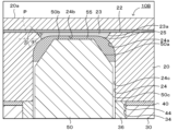
- FIG. 2 is a cross-sectional view showing a schematic configuration of the wafer mounting table 10.
- FIG. 2 is a partially enlarged view of FIG. 5 is an explanatory diagram of a process for joining a terminal 50 and an electrode extraction portion 23.
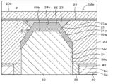
- FIG. FIG. 13 is a partial enlarged view of a wafer mounting table 10B according to another embodiment.
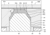
- FIG. 10 is a partial enlarged view of a wafer mounting table 10C according to another embodiment.
- FIG. 10 is a partial enlarged view of a wafer mounting table 10D according to another embodiment.
- 10 is a partial enlarged view of a wafer mounting table 10E according to another embodiment of the present invention.
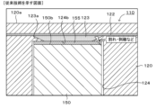
- FIG. 4 is a partial enlarged view of a wafer mounting table 110 according to a comparative example.
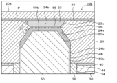
- FIG. 1 is a cross-sectional view showing the schematic configuration of the wafer mounting table 10 of this embodiment (a cross-sectional view when the wafer mounting table 10 is cut along a plane including the central axis of the wafer mounting table 10), and FIG. 2 is an enlarged view of a portion of FIG. 1 (an enlarged view of the area within the frame indicated by the two-dot chain line).
- FIG. 1 is a cross-sectional view showing the schematic configuration of the wafer mounting table 10 of this embodiment (a cross-sectional view when the wafer mounting table 10 is cut along a plane including the central axis of the wafer mounting table 10)
- FIG. 2 is an enlarged view of a portion of FIG. 1 (an enlarged view of the area within the frame indicated by the two-dot chain line).
- the terms up/down, left/right, and front/rear may be used, but these terms merely refer to relative positional relationships.
- the wafer mounting table 10 is an example of a semiconductor manufacturing equipment component used to process a wafer W. As shown in FIG. 1, the wafer mounting table 10 includes a ceramic plate 20, a cooling plate 30, a bonding layer 40, and a terminal 50.
- the ceramic plate 20 is a disk-shaped member having a wafer mounting surface 20a on its upper surface.
- the ceramic plate 20 is formed from a ceramic-containing material.
- a ceramic-containing material is a material whose main component is ceramic, and may contain, in addition to ceramic, components derived from sintering aids (such as rare earth elements) and unavoidable components.
- a main component means that it accounts for 50 mass% or more of the total. Examples of ceramics include alumina and aluminum nitride.
- the electrostatic electrode 22 is embedded in the ceramic plate 20.
- the electrostatic electrode 22 is formed of a material containing a metal such as W, Mo, WC, or MoC.
- the metal used for the electrostatic electrode 22 is preferably one whose thermal expansion coefficient is close to that of the ceramic plate 20. To bring the thermal expansion coefficient of the electrostatic electrode 22 close to that of the ceramic plate 20, the electrostatic electrode 22 may contain the ceramic contained in the ceramic plate 20.
- the electrostatic electrode 22 is a disk-shaped or mesh-shaped monopolar electrostatic electrode.
- the layer of the ceramic plate 20 above the electrostatic electrode 22 functions as a dielectric layer.
- a DC power source 62 for electrostatic adsorption is connected to the electrostatic electrode 22 via a terminal 50.
- the cooling plate 30 is a disk-shaped member having a refrigerant flow path 32 inside which a refrigerant can circulate.
- the refrigerant flow path 32 is formed in a single stroke from one end to the other so that it spreads over the entire surface of the ceramic plate 20 in a plan view.
- One end and the other end of the refrigerant flow path 32 are connected to a refrigerant circulation pump (not shown) that has the function of adjusting the temperature of the refrigerant.
- the cooling plate 30 is made of a conductive material containing, for example, a metal. Examples of the conductive material include composite materials and metals.
- composite materials include metal composite materials (also called metal matrix composites (MMCs)), and examples of MMCs include materials containing Si, SiC, and Ti, and materials in which a SiC porous body is impregnated with Al and/or Si.
- MMCs metal matrix composites
- a material containing Si, SiC, and Ti is called SiSiCTi
- AlSiC a material in which a SiC porous body is impregnated with Al
- SiSiC a material in which a SiC porous body is impregnated with Si
- metals include Al, Ti, Mo, and alloys thereof. It is preferable that the conductive material used for the cooling plate 30 has a thermal expansion coefficient close to that of the ceramic plate 20.
- the bonding layer 40 bonds the lower surface of the ceramic plate 20 to the upper surface of the cooling plate 30.
- the bonding layer 40 may be, for example, a metal bonding layer formed of solder or a metal brazing material.
- the metal bonding layer may be formed, for example, by TCB (thermal compression bonding).
- TCB refers to a known method in which a metal bonding material is sandwiched between two members to be bonded, and the two members are pressure-bonded while being heated to a temperature below the solidus temperature of the metal bonding material.
- An organic adhesive layer may be used as the bonding layer 40 instead of the metal bonding layer.
- the terminal 50 is a metal member that supplies power to the electrostatic electrode 22.
- the terminal 50 is, for example, a metal rod.
- Metals used for the terminal 50 include, for example, W, Mo, Ni, etc., and it is preferable that the thermal expansion coefficient of the metal is close to that of the ceramic plate 20.
- the terminal 50 is inserted from the underside of the cooling plate 30 through the cooling plate through-hole 34 that passes through the cooling plate 30 in the vertical direction and the bonding layer through-hole 44 that passes through the bonding layer 40 in the vertical direction, into the terminal hole 24 provided in the ceramic plate 20.
- the terminal 50 is electrically connected to the electrostatic electrode 22.
- the joining structure between the terminal 50 and the electrostatic electrode 22 will be described with reference to FIG. 2.
- the terminal 50 passes through the inside of the insulating tube 36 arranged in the cooling plate through hole 34 and the joining layer through hole 44, and is inserted with some play into the terminal hole 24.
- the terminal 50 is electrically connected to the electrode extraction part 23 added to the electrostatic electrode 22 via a conductive joining part 55.
- the conductive joining part 55 may be a metal joining layer formed of solder or metal brazing material.
- the electrode extraction portion 23 is a disk-shaped member embedded in the ceramic plate 20 and facing downward from the electrostatic electrode 22.
- the electrode extraction portion 23 is formed of a material containing a metal such as W, Mo, WC, or MoC.
- the metal used for the electrode extraction portion 23 is preferably one whose thermal expansion coefficient is close to that of the ceramic plate 20. In order to bring the thermal expansion coefficient of the electrode extraction portion 23 close to that of the ceramic plate 20, the electrode extraction portion 23 may contain the ceramic contained in the ceramic plate 20.
- the electrode extraction portion 23 may be formed of a material having the same composition as the electrostatic electrode 22.
- the electrode extraction portion 23 is in the shape of a spherical trapezoid, and its side surface 23a tapers downward. The electrode extraction portion 23 is exposed to the bottom surface 24b of the terminal hole 24.
- the terminal hole 24 is a cylindrical hole that is provided so as to reach the electrode extraction portion 23 from the underside of the ceramic plate 20.
- the terminal hole 24 has a terminal hole reduced diameter surface 24a that reduces in diameter toward the bottom of the hole.
- the terminal hole reduced diameter surface 24a is provided between the bottom surface 24b and the side surface 24c of the terminal hole 24, and forms a C-surface (tapered surface) in the shape of a C-chamfered edge at the boundary between the bottom surface 24b and the side surface 24c of the terminal hole 24.
- FIG. 8 is a partial enlarged view of the wafer mounting table 110 in a comparative embodiment (the embodiment of the prior art disclosed in Patent Document 1).
- the terminal 150 is electrically connected to the electrode extraction portion 123 embedded in the ceramic plate 120 together with the electrostatic electrode 122 via a conductive joint 155.
- the electrode extraction portion 123 has a truncated cone shape, and its side surface 123a is reduced in diameter toward the bottom. The electrode extraction portion 123 is exposed to the bottom surface 124b of the terminal hole 124.
- the terminal hole 124 is a cylindrical hole and is provided so as to reach the electrode extraction portion 123 from the lower surface of the ceramic plate 120.
- the bottom surface 124b of the terminal hole 124 is flat, and the bottom surface 124b of the terminal hole 124 intersects with the side surface 123a of the electrode extraction portion 123. Therefore, the ceramic plate 120 between the inclined side surface 123a of the electrode extraction portion 123 and the flat bottom surface 124b of the terminal hole 124 becomes thin. Then, this portion may be damaged by cracking or peeling under the load of drilling the terminal hole 124 or joining the electrostatic electrode 122 and the terminal 150.
- the ceramic plate 20 between the electrode extraction portion 23 and the terminal hole 24 can be made thicker by the inclination of the terminal hole reduced diameter surface 24a, for example, by the angle ⁇ described later. Therefore, the ceramic plate 20 is prevented from becoming thin, and damage to the wafer mounting table 10 can be prevented.
- the angle ⁇ between the imaginary plane P parallel to the electrostatic electrode 22 and the terminal hole reduced diameter surface 24a is preferably, for example, 20° or more and 75° or less.
- the intersection angle ⁇ between the terminal hole reduced diameter surface 24a and the side surface 23a of the electrode extraction portion 23 is preferably, for example, 40° or more and 120° or less.
- the inclination angle ⁇ of the side surface 23a of the electrode extraction portion 23 is preferably smaller than the intersection angle ⁇ between the terminal hole reduced diameter surface 24a and the side surface 23a of the electrode extraction portion 23.
- the angle ⁇ or angle ⁇ can be obtained using the tangent of the terminal hole reduced diameter surface 24a at the intersection 25, and when the side surface 23a of the electrode extraction portion 23 is a curved surface, the angle ⁇ or angle ⁇ can be obtained using the tangent of the side surface 23a of the electrode extraction portion 23 at the intersection 25.
- the angle ⁇ can be determined using the tangent line of the side surface 23a of the electrode extraction portion 23 at the point where the lower surface of the electrostatic electrode 22 and the side surface 23a of the electrode extraction portion 23 intersect.
- the terminal hole reduced diameter surface 24a is provided so as to extend into the electrode extraction portion 23. Therefore, the electrode extraction portion 23 is exposed not only on the bottom surface 24b of the terminal hole 24 but also on a portion of the terminal hole reduced diameter surface 24a.
- the terminal 50 has a terminal reduced diameter surface 50a that reduces in diameter toward the tip.
- the terminal reduced diameter surface 50a is provided between the tip surface 50b and the side surface 50c of the terminal 50, and is a C surface (tapered surface) formed by chamfering the edge of the boundary between the tip surface 50b and the side surface 50c of the terminal 50.
- the conductive joint 55 is arranged not only between the bottom surface 24b of the terminal hole 24 and the tip surface 50b of the terminal 50, but also between the terminal hole reduced diameter surface 24a and the terminal reduced diameter surface 50a, and the terminal hole reduced diameter surface 24a and the terminal reduced diameter surface 50a are joined by the conductive joint 55.
- the terminal 50 is joined to the electrode extraction portion 23 exposed at the bottom surface 24b and the terminal hole reduced diameter surface 24a of the terminal hole 24, and is also joined to the ceramic plate 20.
- the wafer mounting table 10 is installed in a vacuum chamber (not shown), and the wafer W is mounted on the wafer mounting surface 20a of the wafer mounting table 10. Then, a voltage is applied from the DC power supply 62 to the electrostatic electrode 22 via the terminal 50. Then, the wafer W is attracted and fixed to the wafer mounting surface 20a. Then, the inside of the vacuum chamber is set to a vacuum atmosphere or a reduced pressure atmosphere, and the wafer W is processed in the vacuum chamber.
- an upper electrode equipped with a shower head is placed on the ceiling of the vacuum chamber, and a high frequency voltage is applied between the upper electrode and the cooling plate 30 while a reactive gas is supplied from the shower head to the space between the wafer W and the upper electrode to generate plasma.
- the application of the voltage to the electrostatic electrode 22 is released.
- the wafer W is released from the attraction and fixation to the wafer mounting surface 20a.
- a coolant is passed through the coolant flow passage 32 when it is necessary to lower the temperature of the wafer W.
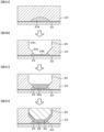
- FIG. 3 is an explanatory diagram of this process.
- a ceramic plate 20 is prepared in which an electrostatic electrode 22 and a disk member 23z added to the electrostatic electrode 22 are embedded (FIG. 3A).
- the disk member 23z is a member that will become the electrode extraction portion 23 by later drilling.
- the disk member 23z is a member with a spherical or spherical truncated shape that decreases in diameter as it moves away from the electrostatic electrode 22.
- Such a ceramic plate 20 can be prepared, for example, as follows. First, two disk molded bodies of ceramic powder are prepared. Next, a printed electrode having the same shape as the electrostatic electrode 22 is printed on the upper surface of the first disk molded body so that it is concentric with the disk molded body.
- a printed electrode having the same shape as the disk member 23z is printed at a predetermined position on the upper surface of this printed electrode. Then, a second disk molded body is stacked on the printed electrode surface of the first disk molded body to form a laminate. This laminate is hot-pressed and fired to obtain a ceramic plate 20. In addition, in Figures 3A to 3D, the surface of the ceramic plate 20 that will become the wafer mounting surface 20a faces downward.
- a terminal hole 24 is formed that reaches the electrode extraction portion 23 from one surface of the ceramic plate 20 (Fig. 3B).
- the terminal hole 24 has a terminal hole reduced diameter surface 24a between the bottom surface 24b and the side surface 24c.
- the terminal hole 24 is formed so that the bottom surface 24b and a part of the terminal hole reduced diameter surface 24a of the terminal hole 24 enter the disk member 23z, and the electrode extraction portion 23 is exposed at the bottom surface 24b of the terminal hole 24 and a part of the terminal hole reduced diameter surface 24a.
- the terminal hole 24 can be formed by a known drilling process, such as drilling or laser processing.
- a conductive bonding material 55z is placed at the bottom of the terminal hole 24 (FIG. 3C).
- the bonding material 55z will later become the conductive bonding portion 55, and may be, for example, a metal sheet formed from solder or a metal brazing material.
- the terminal 50 is placed on the bonding material 55z, and the bonding material 55z is sandwiched between the terminal hole 24 and the terminal 50.
- the bonding material 55z is treated in this state at a temperature equal to or higher than its melting point, the bonding material 55z melts and spreads between the terminal hole 24 and the terminal 50.
- the bonding material 55z solidifies in this state, the electrode extraction portion 23 exposed in the terminal hole 24 and the terminal 50 are bonded by the conductive bonding portion 55 ( Figure 3D). This electrically connects the terminal 50 and the electrostatic electrode 22.
- the terminal hole 24 has a terminal hole narrowing surface 24a that narrows toward the bottom of the hole, and the terminal hole narrowing surface 24a is arranged to intersect with the side surface 23a of the electrode extraction portion 23. This prevents the ceramic plate 20 from becoming thin, and prevents damage to the wafer mounting table 10.
- the side surface 23a of the electrode extraction portion 23 tapers downward. This allows the volume of the electrode extraction portion 23 to be reduced while still ensuring the contact area between the electrostatic electrode 22 and the electrode extraction portion 23. Reducing the volume of the electrode extraction portion 23 can suppress cracking or peeling of the ceramic plate 20 caused by the difference in thermal expansion between the ceramic plate 20 and the electrode extraction portion 23.
- the angle ⁇ between the imaginary plane P parallel to the electrostatic electrode 22 and the terminal hole reduced diameter surface 24a may be 20° or more and 75° or less. If this angle ⁇ is 20° or more, thin portions are less likely to form in the ceramic plate 20, so cracking and peeling of the ceramic plate 20 can be further suppressed. If this angle ⁇ is 75° or less, the hole diameter of the terminal hole 24 can be relatively large even if the bottom of the terminal hole 24 is made small in diameter according to the size of the electrode extraction portion 23, for example. This allows the terminal diameter of the terminal 50 inserted into the terminal hole 24 to be large, ensuring good conductivity.
- intersection angle ⁇ between the terminal hole reduced diameter surface 24a and the side surface 23a of the electrode lead-out portion 23 may be 40° or more and 120° or less. If this intersection angle ⁇ is 40° or more, thin portions are less likely to form in the ceramic plate 20, so cracking and peeling of the ceramic plate 20 can be further suppressed. If this intersection angle is 120° or less, the hole diameter of the terminal hole 24 can be made relatively large even if the bottom of the terminal hole 24 is made small in diameter according to the size of the electrode lead-out portion 23, for example. This allows the terminal diameter of the terminal 50 inserted into the terminal hole 24 to be large, ensuring good conductivity.
- the inclination angle ⁇ of the side surface 23a of the electrode extraction portion 23 may be smaller than the intersection angle ⁇ between the terminal hole reduced diameter surface 24a and the side surface 23a of the electrode extraction portion 23.
- terminal hole reduced diameter surface 23a extends into the electrode extraction portion 23. This makes it easier to ensure a sufficient contact area between the electrode extraction portion 23 and the conductive joint portion 55, improving electrical conductivity.
- the terminal hole reduced diameter surface 24a is a C-shaped surface provided between the bottom surface 24b and the side surface 24c of the terminal hole 24, and the terminal 50 has a terminal reduced diameter surface 50a that reduces in diameter toward the tip of the terminal 50, the terminal reduced diameter surface 50a being a C-shaped surface provided between the tip surface 50b and the side surface 50c of the terminal 50, and the terminal hole reduced diameter surface 24a and the terminal reduced diameter surface 50a are joined by a conductive joint 55.
- the C-shaped terminal hole reduced diameter surface 24a can be joined by receiving the C-shaped terminal reduced diameter surface 50a, which prevents the pressing force from the terminal 50 from concentrating on the bottom surface 24b of the terminal hole 24, and prevents the ceramic plate 20 from cracking or peeling around the bottom surface 24b of the terminal hole 24.
- the size of the C surface of the terminal hole narrowing surface 24a and the size of the C surface of the terminal narrowing surface 50a are equal, and it is also preferable that the inclination of the C surface of the terminal hole narrowing surface 24a and the inclination of the C surface of the terminal narrowing surface 50a are equal.
- the inclination of the C surface of the terminal hole narrowing surface 24a and the terminal narrowing surface 50a may be, for example, 30° or more and 60° or less.
- the size of the C surface of the terminal hole narrowing surface 24a and the terminal narrowing surface 50a may be, for example, 0.3 mm or more and 2.5 mm or less.
- the diameter of the bottom surface 24b of the terminal hole 24 may be smaller than the diameter of the side surface 50c of the terminal 50, and may be smaller than the diameter of the bottom surface 50b of the terminal 50.
- the terminal hole reduced diameter surface 24a is a C-surface formed by chamfering the edge of the boundary between the bottom surface 24b and the side surface 24c of the terminal hole 24, but is not limited to this.
- the terminal hole reduced diameter surface 24a may be an R-surface formed by chamfering the edge of the boundary between the bottom surface 24b and the side surface 24c of the terminal hole 24.
- the bottom surface 24b of the terminal hole 24 may be an R-surface, and the R-surface-shaped bottom surface 24b may also serve as the terminal hole reduced diameter surface 24a.
- the radius of curvature of the R-surface of the terminal hole reduced diameter surface 24a may be, for example, 0.3 mm or more and 2.5 mm or less.
- the same components as those in the above-described embodiment are given the same reference numerals.
- the electrode extraction portion 23 has a spherical truncated shape, but is not limited thereto.
- the electrode extraction portion 23 may have a conical truncated shape. In that case, in the step of joining the terminal 50 and the electrostatic electrode 22, a conical or truncated conical member may be used as the disk member 23z.
- the electrode extraction portion 23 may have a cylindrical shape. In that case, in the step of joining the terminal 50 and the electrostatic electrode 22, a cylindrical member may be used as the disk member 23z. Note that in FIGS. 5 and 6, the same reference numerals are used for the same components as in the above-described embodiment.
- the terminal hole reduced diameter surface 24a is provided so as to enter the electrode extraction portion 23, but is not limited to this.
- the terminal hole reduced diameter surface 24a may be provided so as to abut against the side surface 23a of the electrode extraction portion 23 without entering the electrode extraction portion 23. Note that in FIG. 7, the same reference numerals are used for the same components as in the above-described embodiment.
- the terminal reduced diameter surface 50a is a C-surface formed by chamfering the edge of the boundary between the tip surface 50b and the side surface 50c of the terminal 50, but is not limited to this.
- the terminal reduced diameter surface 50a may be an R-surface formed by chamfering the edge of the boundary between the tip surface 50b and the side surface 50c of the terminal 50.
- the tip surface 50b of the terminal 50 may be an R-surface, and the R-surface-shaped tip surface 50b may also serve as the terminal reduced diameter surface 50a.
- the radius of curvature of the R-surface of the terminal reduced diameter surface 50a may be, for example, 0.3 mm or more and 2.5 mm or less.
- the terminal 50 may not have a terminal reduced diameter surface 50a, and the tip surface 50b and the side surface 50c may intersect at a right angle.
- the conductive joint 55 only needs to be able to join the terminal 50 and the electrode lead-out portion 23 to electrically connect the two, and may, for example, be disposed only between the electrode lead-out portion 23 exposed at the bottom surface 24b of the terminal hole 24 and the tip surface 50b of the terminal 50, or may be disposed only between the electrode lead-out portion 23 exposed at the terminal hole reduced diameter surface 24a and the terminal reduced diameter surface 50a.
- a metal rod is used as the terminal 50, but this is not particularly limited and the terminal 50 may be, for example, a metal cable.
- the wafer mounting table 10 may have at least one of a heater electrode and an RF electrode (electrode for generating plasma) embedded in the ceramic plate 20 instead of or in addition to the electrostatic electrode 22.
- the joining structure between the heater electrode and the terminal for the heater electrode and the joining structure between the RF electrode and the terminal for the RF electrode may be the same as the joining structure between the electrostatic electrode 22 and the terminal 50 described above.
- the present invention can be used in semiconductor manufacturing equipment used to process wafers.
- 10, 10B, 10C, 10D, 10E wafer mounting table 20 ceramic plate, 20a wafer mounting surface, 22 electrostatic electrode, 23 electrode extraction portion, 23a side surface, 23z disk member, 24 terminal hole, 24a terminal hole diameter reduction surface, 24b bottom surface, 24c side surface, 25 boundary portion, 30 cooling plate, 32 refrigerant flow path, 34 cooling plate through hole, 35 adhesive layer, 36 insulating tube, 40 bonding layer, 44 bonding layer through hole, 50 terminal, 50a terminal diameter reduction surface, 50b tip surface, 50c side surface, 55 conductive bonding portion, 55z bonding material, 62 DC power source, 110 wafer mounting table, 120 ceramic plate, 120a wafer mounting surface, 122 electrostatic electrode, 123 electrode lead-out portion, 123a side surface, 124 terminal hole, 124b bottom surface, 150 terminal, 150b tip surface, 155 conductive bonding portion.
Landscapes
- Physics & Mathematics (AREA)
- Engineering & Computer Science (AREA)
- Plasma & Fusion (AREA)
- Chemical & Material Sciences (AREA)
- Analytical Chemistry (AREA)
- Container, Conveyance, Adherence, Positioning, Of Wafer (AREA)
Abstract
Selon la présente invention, une table de placement de tranche 10 comprend : une plaque en céramique 20 ayant, sur une surface supérieure de celle-ci, une surface de placement de tranche 20a ; une électrode électrostatique 22 incorporée dans la plaque en céramique 20 ; une partie d'extraction d'électrode 23 incorporée dans la plaque en céramique 20 et disposée en regard vers le bas à partir de l'électrode électrostatique 22 ; un trou de borne 24 disposé de façon à atteindre la partie d'extraction d'électrode 23 à partir d'une surface inférieure de la plaque en céramique 20 ; une borne 50 insérée dans le trou de borne 24 ; et une partie de jonction conductrice 55 disposée entre la borne 50 et la partie d'extraction d'électrode 23 et joignant la borne 50 et la partie d'extraction d'électrode 23. Le trou de borne 24 a une surface de diamètre réduit de trou de borne 24a dont le diamètre est réduit en direction du fond de trou. La surface de diamètre réduit de trou de borne 24a est disposée de façon à croiser une surface latérale 23a de la partie d'extraction d'électrode 23.
Priority Applications (5)
| Application Number | Priority Date | Filing Date | Title |
|---|---|---|---|
| CN202380013327.XA CN121753541A (zh) | 2023-08-22 | 2023-08-22 | 半导体制造装置用部件 |
| PCT/JP2023/030114 WO2025041254A1 (fr) | 2023-08-22 | 2023-08-22 | Élément pour dispositif de fabrication de semi-conducteur |
| JP2024510732A JP7691578B1 (ja) | 2023-08-22 | 2023-08-22 | 半導体製造装置用部材 |
| US18/583,974 US12519001B2 (en) | 2023-08-22 | 2024-02-22 | Member for semiconductor manufacturing apparatus |
| TW113107206A TW202510181A (zh) | 2023-08-22 | 2024-02-29 | 半導體製造裝置用零件 |
Applications Claiming Priority (1)
| Application Number | Priority Date | Filing Date | Title |
|---|---|---|---|
| PCT/JP2023/030114 WO2025041254A1 (fr) | 2023-08-22 | 2023-08-22 | Élément pour dispositif de fabrication de semi-conducteur |
Related Child Applications (1)
| Application Number | Title | Priority Date | Filing Date |
|---|---|---|---|
| US18/583,974 Continuation US12519001B2 (en) | 2023-08-22 | 2024-02-22 | Member for semiconductor manufacturing apparatus |
Publications (1)
| Publication Number | Publication Date |
|---|---|
| WO2025041254A1 true WO2025041254A1 (fr) | 2025-02-27 |
Family
ID=94689006
Family Applications (1)
| Application Number | Title | Priority Date | Filing Date |
|---|---|---|---|
| PCT/JP2023/030114 Pending WO2025041254A1 (fr) | 2023-08-22 | 2023-08-22 | Élément pour dispositif de fabrication de semi-conducteur |
Country Status (5)
| Country | Link |
|---|---|
| US (1) | US12519001B2 (fr) |
| JP (1) | JP7691578B1 (fr) |
| CN (1) | CN121753541A (fr) |
| TW (1) | TW202510181A (fr) |
| WO (1) | WO2025041254A1 (fr) |
Citations (5)
| Publication number | Priority date | Publication date | Assignee | Title |
|---|---|---|---|---|
| JP2008135737A (ja) * | 2006-11-01 | 2008-06-12 | Ngk Insulators Ltd | 静電チャック及び静電チャックの製造方法 |
| JP2012039011A (ja) * | 2010-08-10 | 2012-02-23 | Covalent Materials Corp | 静電チャックおよびその製造方法。 |
| JP2012049185A (ja) * | 2010-08-24 | 2012-03-08 | Taiheiyo Cement Corp | セラミックス部材及びその製造方法 |
| JP2013084938A (ja) * | 2011-09-30 | 2013-05-09 | Toto Ltd | 静電チャック |
| WO2021075240A1 (fr) * | 2019-10-18 | 2021-04-22 | 京セラ株式会社 | Structure et dispositif de chauffage |
Family Cites Families (5)
| Publication number | Priority date | Publication date | Assignee | Title |
|---|---|---|---|---|
| US7633738B2 (en) | 2006-11-01 | 2009-12-15 | Ngk Insulators, Ltd. | Electrostatic chuck and manufacturing method thereof |
| JP2017103389A (ja) * | 2015-12-03 | 2017-06-08 | 新光電気工業株式会社 | 静電チャック及び半導体製造装置 |
| JP7372271B2 (ja) * | 2021-01-06 | 2023-10-31 | 日本碍子株式会社 | 半導体製造装置用部材及びその製法 |
| JP7429208B2 (ja) * | 2021-08-17 | 2024-02-07 | 日本碍子株式会社 | ウエハ載置台 |
| JP7514805B2 (ja) * | 2021-08-17 | 2024-07-11 | 日本碍子株式会社 | ウエハ載置台 |
-
2023
- 2023-08-22 WO PCT/JP2023/030114 patent/WO2025041254A1/fr active Pending
- 2023-08-22 JP JP2024510732A patent/JP7691578B1/ja active Active
- 2023-08-22 CN CN202380013327.XA patent/CN121753541A/zh active Pending
-
2024
- 2024-02-22 US US18/583,974 patent/US12519001B2/en active Active
- 2024-02-29 TW TW113107206A patent/TW202510181A/zh unknown
Patent Citations (5)
| Publication number | Priority date | Publication date | Assignee | Title |
|---|---|---|---|---|
| JP2008135737A (ja) * | 2006-11-01 | 2008-06-12 | Ngk Insulators Ltd | 静電チャック及び静電チャックの製造方法 |
| JP2012039011A (ja) * | 2010-08-10 | 2012-02-23 | Covalent Materials Corp | 静電チャックおよびその製造方法。 |
| JP2012049185A (ja) * | 2010-08-24 | 2012-03-08 | Taiheiyo Cement Corp | セラミックス部材及びその製造方法 |
| JP2013084938A (ja) * | 2011-09-30 | 2013-05-09 | Toto Ltd | 静電チャック |
| WO2021075240A1 (fr) * | 2019-10-18 | 2021-04-22 | 京セラ株式会社 | Structure et dispositif de chauffage |
Also Published As
| Publication number | Publication date |
|---|---|
| US12519001B2 (en) | 2026-01-06 |
| US20250069929A1 (en) | 2025-02-27 |
| CN121753541A (zh) | 2026-03-27 |
| JP7691578B1 (ja) | 2025-06-11 |
| TW202510181A (zh) | 2025-03-01 |
| JPWO2025041254A1 (fr) | 2025-02-27 |
Similar Documents
| Publication | Publication Date | Title |
|---|---|---|
| JP4034145B2 (ja) | サセプタ装置 | |
| WO2018038044A1 (fr) | Base de montage de tranche | |
| JP4858319B2 (ja) | ウェハ保持体の電極接続構造 | |
| KR102699791B1 (ko) | 반도체 제조 장치용 부재 | |
| KR20230053499A (ko) | 웨이퍼 배치대 | |
| JP2018006737A (ja) | 保持装置および保持装置の製造方法 | |
| JP4331427B2 (ja) | 半導体製造装置に使用される給電用電極部材 | |
| JP4331983B2 (ja) | ウェハ支持部材およびその製造方法 | |
| JP7691578B1 (ja) | 半導体製造装置用部材 | |
| JP3906087B2 (ja) | ウエハ支持部材 | |
| JP7657310B2 (ja) | ウエハ載置台 | |
| KR20260055984A (ko) | 반도체 제조 장치용 부재 | |
| JP7606635B1 (ja) | 半導体製造装置用部材 | |
| JP7634493B2 (ja) | 給電部材及びウエハ載置台 | |
| JP7675282B1 (ja) | ウエハ載置台 | |
| JP7614405B1 (ja) | 給電部材及びウエハ載置台 | |
| US12622225B2 (en) | Member for semiconductor manufacturing apparatus | |
| KR102961425B1 (ko) | 반도체 제조 장치용 부재 | |
| WO2025041221A1 (fr) | Élément pour dispositif de fabrication de semi-conducteurs | |
| JP2024139299A (ja) | 保持装置 |
Legal Events
| Date | Code | Title | Description |
|---|---|---|---|
| ENP | Entry into the national phase |
Ref document number: 2024510732 Country of ref document: JP Kind code of ref document: A |
|
| WWE | Wipo information: entry into national phase |
Ref document number: 2024510732 Country of ref document: JP |
|
| 121 | Ep: the epo has been informed by wipo that ep was designated in this application |
Ref document number: 23949715 Country of ref document: EP Kind code of ref document: A1 |
|
| NENP | Non-entry into the national phase |
Ref country code: DE |