WO2025041221A1 - Élément pour dispositif de fabrication de semi-conducteurs - Google Patents
Élément pour dispositif de fabrication de semi-conducteurs Download PDFInfo
- Publication number
- WO2025041221A1 WO2025041221A1 PCT/JP2023/029982 JP2023029982W WO2025041221A1 WO 2025041221 A1 WO2025041221 A1 WO 2025041221A1 JP 2023029982 W JP2023029982 W JP 2023029982W WO 2025041221 A1 WO2025041221 A1 WO 2025041221A1
- Authority
- WO
- WIPO (PCT)
- Prior art keywords
- mounting surface
- wafer
- focus ring
- semiconductor manufacturing
- manufacturing equipment
- Prior art date
- Legal status (The legal status is an assumption and is not a legal conclusion. Google has not performed a legal analysis and makes no representation as to the accuracy of the status listed.)
- Pending
Links
Images
Classifications
-
- H—ELECTRICITY
- H01—ELECTRIC ELEMENTS
- H01J—ELECTRIC DISCHARGE TUBES OR DISCHARGE LAMPS
- H01J37/00—Discharge tubes with provision for introducing objects or material to be exposed to the discharge, e.g. for the purpose of examination or processing thereof
- H01J37/32—Gas-filled discharge tubes
- H01J37/32431—Constructional details of the reactor
- H01J37/32715—Workpiece holder
- H01J37/32724—Temperature
-
- H—ELECTRICITY
- H01—ELECTRIC ELEMENTS
- H01J—ELECTRIC DISCHARGE TUBES OR DISCHARGE LAMPS
- H01J37/00—Discharge tubes with provision for introducing objects or material to be exposed to the discharge, e.g. for the purpose of examination or processing thereof
- H01J37/32—Gas-filled discharge tubes
- H01J37/32431—Constructional details of the reactor
- H01J37/32623—Mechanical discharge control means
- H01J37/32642—Focus rings
-
- H—ELECTRICITY
- H10—SEMICONDUCTOR DEVICES; ELECTRIC SOLID-STATE DEVICES NOT OTHERWISE PROVIDED FOR
- H10P—GENERIC PROCESSES OR APPARATUS FOR THE MANUFACTURE OR TREATMENT OF DEVICES COVERED BY CLASS H10
- H10P72/00—Handling or holding of wafers, substrates or devices during manufacture or treatment thereof
- H10P72/70—Handling or holding of wafers, substrates or devices during manufacture or treatment thereof for supporting or gripping
- H10P72/76—Handling or holding of wafers, substrates or devices during manufacture or treatment thereof for supporting or gripping using mechanical means, e.g. clamps or pinches
- H10P72/7604—Handling or holding of wafers, substrates or devices during manufacture or treatment thereof for supporting or gripping using mechanical means, e.g. clamps or pinches the wafers being placed on a susceptor, stage or support
- H10P72/7606—Handling or holding of wafers, substrates or devices during manufacture or treatment thereof for supporting or gripping using mechanical means, e.g. clamps or pinches the wafers being placed on a susceptor, stage or support characterised by edge clamping, e.g. clamping ring
-
- H—ELECTRICITY
- H01—ELECTRIC ELEMENTS
- H01J—ELECTRIC DISCHARGE TUBES OR DISCHARGE LAMPS
- H01J2237/00—Discharge tubes exposing object to beam, e.g. for analysis treatment, etching, imaging
- H01J2237/32—Processing objects by plasma generation
- H01J2237/33—Processing objects by plasma generation characterised by the type of processing
- H01J2237/332—Coating
- H01J2237/3321—CVD [Chemical Vapor Deposition]
-
- H—ELECTRICITY
- H01—ELECTRIC ELEMENTS
- H01J—ELECTRIC DISCHARGE TUBES OR DISCHARGE LAMPS
- H01J2237/00—Discharge tubes exposing object to beam, e.g. for analysis treatment, etching, imaging
- H01J2237/32—Processing objects by plasma generation
- H01J2237/33—Processing objects by plasma generation characterised by the type of processing
- H01J2237/334—Etching
Definitions
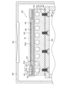
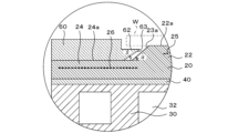
- the semiconductor manufacturing equipment component disclosed in Patent Document 1 includes a ceramic plate and a cooling plate provided on the underside of the ceramic plate.
- the ceramic plate has a circular wafer mounting surface provided on the upper surface, and an annular focus ring mounting surface provided on the outer periphery of the wafer mounting surface, one step lower than the wafer mounting surface.
- the connecting portion connecting the wafer mounting surface and the focus ring mounting surface has a side surface perpendicular to the wafer mounting surface.
- the focus ring mounted on the focus ring mounting surface has a step along the inner periphery of its upper end so as not to interfere with the wafer.
- the wafer mounted on the wafer mounting surface is placed in a state where it overhangs the wafer mounting surface.
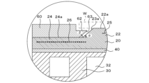
- the angle ⁇ is preferably 20° or more. If the angle ⁇ is 20° or more, the tip of the FR 60 does not become too acute, and concerns about cracking of the FR 60 are reduced, which is preferable.
- the diameter of the wafer mounting surface 22a is smaller than the diameter of the wafer W (e.g., 300 mm).
- FR60 is an annular member placed on the FR mounting surface 24a, and is made of, for example, silicon.
- a step 62 is provided along the circumferential direction at the upper part of the inner peripheral surface of FR60. The step 62 is provided to prevent the wafer W from interfering with FR60.
- a portion 63 of the inner peripheral surface of FR60 facing the tapered surface 23a is a side surface of a truncated cone (tapered surface) whose diameter increases from top to bottom. This portion 63 is not in contact with the tapered surface 23a. In other words, a gap is formed between this portion 63 and the tapered surface 23a. Therefore, FR60 is not easily affected by the heat of the truncated cone portion 22 of the ceramic plate 20.
- the angle ⁇ (see FIG. 3) of portion 63 with respect to the FR mounting surface 24a is the same as the angle ⁇ of tapered surface 23a with respect to the FR mounting surface 24a.
- the bolt 90 is inserted from below into a stepped bolt insertion hole 86 that penetrates the installation plate 84 in the vertical direction, and the foot is screwed into the screw hole 34 provided on the lower surface of the cooling plate 30. At this time, the head of the bolt 90 engages with the stepped portion of the bolt insertion hole 86.
- the O-ring 88 is crushed in the vertical direction to exert a sealing property. If there are other areas that require sealing, place separate O-rings in those areas as well.
- the FR 60 is placed on the FR placement surface 24a of the semiconductor manufacturing equipment member 10, and the disk-shaped wafer W is placed on the wafer placement surface 22a.
- a DC voltage is applied to the wafer adsorption electrode 25 to adsorb the wafer W to the wafer placement surface 22a
- a DC voltage is applied to the FR adsorption electrode 26 to adsorb the FR 60 to the FR placement surface 24a.
- the interior of the chamber 80 is then set to a predetermined vacuum atmosphere (or reduced pressure atmosphere), and a high-frequency voltage is applied between the shower head 82 and the cooling plate 30 while supplying process gas from the shower head 82. This generates plasma between the cooling plate 30 and the shower head 82.
- the wafer W is then processed using this plasma.
- the FR 60 is also consumed as the wafers W are plasma processed, but since the FR 60 is thicker than the wafers W, the FR 60 is replaced after processing multiple wafers W.
- the connecting portion (frustum portion 22) connecting the wafer mounting surface 22a and the FR mounting surface 24a has a side surface (tapered surface 23a) of the truncated cone whose diameter increases from the wafer mounting surface 22a toward the FR mounting surface 24a. Therefore, compared to when the side surface of the connecting portion is perpendicular to the wafer mounting surface 22a, the thermal path from the outer periphery of the wafer mounting surface 22a toward the cooling plate 30 increases.
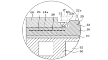
- FIG. 4 is a partially enlarged view of a comparative embodiment (the embodiment of the prior art disclosed in Patent Document 1).
- the ceramic plate 20 is formed in a shape in which flat, small-diameter cylindrical portions 122 are stacked on the upper surface of a flat cylindrical portion 24.
- the upper surface of the cylindrical portion 122 is the wafer mounting surface 22a.
- the cylindrical portion 122 is also a connecting portion that connects the wafer mounting surface 22a and the FR mounting surface 24a.
- the connecting portion has a side surface (vertical surface 123a) of the cylindrical portion 122.
- a portion 163 of the inner peripheral surface of the FR 60 that faces the vertical surface 123a is also a vertical surface.
- the angle ⁇ of the tapered surface 23a relative to the FR mounting surface 24a is 70° or less. This sufficiently increases the thermal path from the outer periphery of the wafer mounting surface 22a to the cooling plate 30.
- both the side of the connecting portion (frustum portion 22) of the ceramic plate 20 and the portion 63 of the inner peripheral surface of the FR 60 are tapered, when the FR 60 is placed on the FR placement surface 24a, the self-alignment effect improves the placement position accuracy of the FR 60.
- the angle ⁇ of the tapered surface 23a relative to the FR mounting surface 24a and the angle ⁇ of the portion 63 (tapered surface) relative to the FR mounting surface 24a are the same, but this is not particularly limited, and the configurations shown in Figures 5 and 6, for example, may be adopted.
- the same reference numerals are used for the same components as in the embodiment described above.
- the angle ⁇ of portion 63 (tapered surface) relative to FR mounting surface 24a is greater than the angle ⁇ of tapered surface 23a relative to FR mounting surface 24a (i.e., ⁇ > ⁇ ). In this way, the gap between portion 63 (tapered surface) of FR 60 and tapered surface 23a of ceramic plate 20 becomes wider the further up, making it easier to prevent portion 63 (tapered surface) of FR 60 from coming into contact with ceramic plate 20.
- the angle ⁇ of portion 63 (tapered surface) relative to FR mounting surface 24a is smaller than the angle ⁇ of tapered surface 23a relative to FR mounting surface 24a (i.e., ⁇ ). This makes it possible to sufficiently reduce the contact area between the lower surface on the inner periphery side of FR 60 and FR mounting surface 24a, and therefore more effectively prevents the inner periphery of FR 60, which generally tends to cool easily, from becoming excessively cold.
Landscapes
- Physics & Mathematics (AREA)
- Engineering & Computer Science (AREA)
- Plasma & Fusion (AREA)
- Chemical & Material Sciences (AREA)
- Analytical Chemistry (AREA)
- Container, Conveyance, Adherence, Positioning, Of Wafer (AREA)
- Drying Of Semiconductors (AREA)
Abstract
Priority Applications (8)
| Application Number | Priority Date | Filing Date | Title |
|---|---|---|---|
| CN202380012896.2A CN121753530A (zh) | 2023-08-21 | 2023-08-21 | 半导体制造装置用部件 |
| JP2024510644A JP7671918B1 (ja) | 2023-08-21 | 2023-08-21 | 半導体製造装置用部材 |
| KR1020267006364A KR20260038955A (ko) | 2023-08-21 | 2023-08-21 | 반도체 제조 장치용 부재 |
| KR1020247008757A KR102934502B1 (ko) | 2023-08-21 | 2023-08-21 | 반도체 제조 장치용 부재 |
| PCT/JP2023/029982 WO2025041221A1 (fr) | 2023-08-21 | 2023-08-21 | Élément pour dispositif de fabrication de semi-conducteurs |
| US18/584,006 US12463023B2 (en) | 2023-08-21 | 2024-02-22 | Member for semiconductor manufacturing apparatus |
| TW113114105A TW202510091A (zh) | 2023-08-21 | 2024-04-16 | 半導體製造裝置用零件 |
| US19/332,181 US20260018393A1 (en) | 2023-08-21 | 2025-09-18 | Member for semiconductor manufacturing apparatus |
Applications Claiming Priority (1)
| Application Number | Priority Date | Filing Date | Title |
|---|---|---|---|
| PCT/JP2023/029982 WO2025041221A1 (fr) | 2023-08-21 | 2023-08-21 | Élément pour dispositif de fabrication de semi-conducteurs |
Related Child Applications (1)
| Application Number | Title | Priority Date | Filing Date |
|---|---|---|---|
| US18/584,006 Continuation US12463023B2 (en) | 2023-08-21 | 2024-02-22 | Member for semiconductor manufacturing apparatus |
Publications (1)
| Publication Number | Publication Date |
|---|---|
| WO2025041221A1 true WO2025041221A1 (fr) | 2025-02-27 |
Family
ID=94689171
Family Applications (1)
| Application Number | Title | Priority Date | Filing Date |
|---|---|---|---|
| PCT/JP2023/029982 Pending WO2025041221A1 (fr) | 2023-08-21 | 2023-08-21 | Élément pour dispositif de fabrication de semi-conducteurs |
Country Status (6)
| Country | Link |
|---|---|
| US (2) | US12463023B2 (fr) |
| JP (1) | JP7671918B1 (fr) |
| KR (2) | KR102934502B1 (fr) |
| CN (1) | CN121753530A (fr) |
| TW (1) | TW202510091A (fr) |
| WO (1) | WO2025041221A1 (fr) |
Citations (10)
| Publication number | Priority date | Publication date | Assignee | Title |
|---|---|---|---|---|
| JPH07106316A (ja) * | 1993-10-04 | 1995-04-21 | Tokyo Electron Ltd | プラズマ処理装置 |
| JP2000173988A (ja) * | 1998-12-01 | 2000-06-23 | Sumitomo Metal Ind Ltd | 基板保持台、及びプラズマ処理装置 |
| JP2002093894A (ja) * | 2000-06-19 | 2002-03-29 | Applied Materials Inc | セラミック基体支持体 |
| JP2009152232A (ja) * | 2007-12-18 | 2009-07-09 | Mitsubishi Materials Corp | ウエハを支持するためのプラズマエッチング装置用複合シリコンリング |
| JP2013512564A (ja) * | 2009-11-30 | 2013-04-11 | ラム リサーチ コーポレーション | 傾斜側壁を備える静電チャック |
| JP2016195108A (ja) * | 2015-03-31 | 2016-11-17 | ラム リサーチ コーポレーションLam Research Corporation | 傾斜した閉じ込めリングを有するプラズマ処理システム及びプラズマ処理構造 |
| JP2016207979A (ja) * | 2015-04-28 | 2016-12-08 | 日本特殊陶業株式会社 | 静電チャック |
| JP2018107433A (ja) * | 2016-12-27 | 2018-07-05 | 東京エレクトロン株式会社 | フォーカスリング及び基板処理装置 |
| JP2019169699A (ja) * | 2018-03-22 | 2019-10-03 | Sppテクノロジーズ株式会社 | フォーカスリング及びこれを備えたプラズマ処理装置 |
| JP2023027641A (ja) * | 2021-08-17 | 2023-03-02 | 日本碍子株式会社 | ウエハ載置台 |
Family Cites Families (5)
| Publication number | Priority date | Publication date | Assignee | Title |
|---|---|---|---|---|
| US5529657A (en) | 1993-10-04 | 1996-06-25 | Tokyo Electron Limited | Plasma processing apparatus |
| KR100292410B1 (ko) * | 1998-09-23 | 2001-06-01 | 윤종용 | 불순물 오염이 억제된 반도체 제조용 반응 챔버 |
| US20180182635A1 (en) | 2016-12-27 | 2018-06-28 | Tokyo Electron Limited | Focus ring and substrate processing apparatus |
| JP2024516149A (ja) * | 2021-04-21 | 2024-04-12 | ラム リサーチ コーポレーション | 基板への裏面堆積防止 |
| KR102904705B1 (ko) * | 2021-11-09 | 2025-12-29 | 삼성전자주식회사 | 포커스 링, 이를 포함하는 기판 처리 장치 및 이를 이용한 기판 처리 방법 |
-
2023
- 2023-08-21 KR KR1020247008757A patent/KR102934502B1/ko active Active
- 2023-08-21 KR KR1020267006364A patent/KR20260038955A/ko active Pending
- 2023-08-21 JP JP2024510644A patent/JP7671918B1/ja active Active
- 2023-08-21 CN CN202380012896.2A patent/CN121753530A/zh active Pending
- 2023-08-21 WO PCT/JP2023/029982 patent/WO2025041221A1/fr active Pending
-
2024
- 2024-02-22 US US18/584,006 patent/US12463023B2/en active Active
- 2024-04-16 TW TW113114105A patent/TW202510091A/zh unknown
-
2025
- 2025-09-18 US US19/332,181 patent/US20260018393A1/en active Pending
Patent Citations (10)
| Publication number | Priority date | Publication date | Assignee | Title |
|---|---|---|---|---|
| JPH07106316A (ja) * | 1993-10-04 | 1995-04-21 | Tokyo Electron Ltd | プラズマ処理装置 |
| JP2000173988A (ja) * | 1998-12-01 | 2000-06-23 | Sumitomo Metal Ind Ltd | 基板保持台、及びプラズマ処理装置 |
| JP2002093894A (ja) * | 2000-06-19 | 2002-03-29 | Applied Materials Inc | セラミック基体支持体 |
| JP2009152232A (ja) * | 2007-12-18 | 2009-07-09 | Mitsubishi Materials Corp | ウエハを支持するためのプラズマエッチング装置用複合シリコンリング |
| JP2013512564A (ja) * | 2009-11-30 | 2013-04-11 | ラム リサーチ コーポレーション | 傾斜側壁を備える静電チャック |
| JP2016195108A (ja) * | 2015-03-31 | 2016-11-17 | ラム リサーチ コーポレーションLam Research Corporation | 傾斜した閉じ込めリングを有するプラズマ処理システム及びプラズマ処理構造 |
| JP2016207979A (ja) * | 2015-04-28 | 2016-12-08 | 日本特殊陶業株式会社 | 静電チャック |
| JP2018107433A (ja) * | 2016-12-27 | 2018-07-05 | 東京エレクトロン株式会社 | フォーカスリング及び基板処理装置 |
| JP2019169699A (ja) * | 2018-03-22 | 2019-10-03 | Sppテクノロジーズ株式会社 | フォーカスリング及びこれを備えたプラズマ処理装置 |
| JP2023027641A (ja) * | 2021-08-17 | 2023-03-02 | 日本碍子株式会社 | ウエハ載置台 |
Also Published As
| Publication number | Publication date |
|---|---|
| US12463023B2 (en) | 2025-11-04 |
| JPWO2025041221A1 (fr) | 2025-02-27 |
| JP7671918B1 (ja) | 2025-05-02 |
| KR20250029010A (ko) | 2025-03-04 |
| US20250069865A1 (en) | 2025-02-27 |
| CN121753530A (zh) | 2026-03-27 |
| US20260018393A1 (en) | 2026-01-15 |
| KR102934502B1 (ko) | 2026-03-06 |
| KR20260038955A (ko) | 2026-03-19 |
| TW202510091A (zh) | 2025-03-01 |
Similar Documents
| Publication | Publication Date | Title |
|---|---|---|
| US20230146815A1 (en) | Wafer placement table | |
| KR102800130B1 (ko) | 웨이퍼 배치대 | |
| KR20230053499A (ko) | 웨이퍼 배치대 | |
| KR20240046104A (ko) | 웨이퍼 배치대 | |
| US12543527B2 (en) | Wafer placement table, and member for semiconductor manufacturing apparatus, using the same | |
| JP7714505B2 (ja) | ウエハ載置台及びそれを用いた半導体製造装置用部材 | |
| JP7671918B1 (ja) | 半導体製造装置用部材 | |
| CN119365972A (zh) | 晶片载放台 | |
| JP7751079B2 (ja) | 半導体製造装置用部材 | |
| KR102875929B1 (ko) | 웨이퍼 배치대 | |
| US12537174B2 (en) | Wafer placement table | |
| JP7503708B1 (ja) | 半導体製造装置用部材 | |
| US20230144107A1 (en) | Wafer placement table | |
| JP7705456B2 (ja) | 半導体製造装置用部材 | |
| KR102718069B1 (ko) | 웨이퍼 배치대 | |
| JP7515018B1 (ja) | 半導体製造装置用部材 | |
| KR102817676B1 (ko) | 웨이퍼 배치대 | |
| US20260128263A1 (en) | Wafer placement table | |
| KR102846887B1 (ko) | 웨이퍼 배치대 | |
| KR20260057568A (ko) | 반도체 제조 장치용 부재 | |
| CN116564779A (zh) | 晶片载放台及采用了该晶片载放台的半导体制造装置用部件 |
Legal Events
| Date | Code | Title | Description |
|---|---|---|---|
| ENP | Entry into the national phase |
Ref document number: 2024510644 Country of ref document: JP Kind code of ref document: A |
|
| WWE | Wipo information: entry into national phase |
Ref document number: 2024510644 Country of ref document: JP |
|
| WWP | Wipo information: published in national office |
Ref document number: 1020247008757 Country of ref document: KR |
|
| 121 | Ep: the epo has been informed by wipo that ep was designated in this application |
Ref document number: 23949682 Country of ref document: EP Kind code of ref document: A1 |
|
| NENP | Non-entry into the national phase |
Ref country code: DE |