WO2025041221A1 - Member for semiconductor manufacturing device - Google Patents
Member for semiconductor manufacturing device Download PDFInfo
- Publication number
- WO2025041221A1 WO2025041221A1 PCT/JP2023/029982 JP2023029982W WO2025041221A1 WO 2025041221 A1 WO2025041221 A1 WO 2025041221A1 JP 2023029982 W JP2023029982 W JP 2023029982W WO 2025041221 A1 WO2025041221 A1 WO 2025041221A1
- Authority
- WO
- WIPO (PCT)
- Prior art keywords
- mounting surface
- wafer
- focus ring
- semiconductor manufacturing
- manufacturing equipment
- Prior art date
- Legal status (The legal status is an assumption and is not a legal conclusion. Google has not performed a legal analysis and makes no representation as to the accuracy of the status listed.)
- Pending
Links
Images
Classifications
-
- H—ELECTRICITY
- H01—ELECTRIC ELEMENTS
- H01J—ELECTRIC DISCHARGE TUBES OR DISCHARGE LAMPS
- H01J37/00—Discharge tubes with provision for introducing objects or material to be exposed to the discharge, e.g. for the purpose of examination or processing thereof
- H01J37/32—Gas-filled discharge tubes
- H01J37/32431—Constructional details of the reactor
- H01J37/32715—Workpiece holder
- H01J37/32724—Temperature
-
- H—ELECTRICITY
- H01—ELECTRIC ELEMENTS
- H01J—ELECTRIC DISCHARGE TUBES OR DISCHARGE LAMPS
- H01J37/00—Discharge tubes with provision for introducing objects or material to be exposed to the discharge, e.g. for the purpose of examination or processing thereof
- H01J37/32—Gas-filled discharge tubes
- H01J37/32431—Constructional details of the reactor
- H01J37/32623—Mechanical discharge control means
- H01J37/32642—Focus rings
-
- H—ELECTRICITY
- H10—SEMICONDUCTOR DEVICES; ELECTRIC SOLID-STATE DEVICES NOT OTHERWISE PROVIDED FOR
- H10P—GENERIC PROCESSES OR APPARATUS FOR THE MANUFACTURE OR TREATMENT OF DEVICES COVERED BY CLASS H10
- H10P72/00—Handling or holding of wafers, substrates or devices during manufacture or treatment thereof
- H10P72/70—Handling or holding of wafers, substrates or devices during manufacture or treatment thereof for supporting or gripping
- H10P72/76—Handling or holding of wafers, substrates or devices during manufacture or treatment thereof for supporting or gripping using mechanical means, e.g. clamps or pinches
- H10P72/7604—Handling or holding of wafers, substrates or devices during manufacture or treatment thereof for supporting or gripping using mechanical means, e.g. clamps or pinches the wafers being placed on a susceptor, stage or support
- H10P72/7606—Handling or holding of wafers, substrates or devices during manufacture or treatment thereof for supporting or gripping using mechanical means, e.g. clamps or pinches the wafers being placed on a susceptor, stage or support characterised by edge clamping, e.g. clamping ring
-
- H—ELECTRICITY
- H01—ELECTRIC ELEMENTS
- H01J—ELECTRIC DISCHARGE TUBES OR DISCHARGE LAMPS
- H01J2237/00—Discharge tubes exposing object to beam, e.g. for analysis treatment, etching, imaging
- H01J2237/32—Processing objects by plasma generation
- H01J2237/33—Processing objects by plasma generation characterised by the type of processing
- H01J2237/332—Coating
- H01J2237/3321—CVD [Chemical Vapor Deposition]
-
- H—ELECTRICITY
- H01—ELECTRIC ELEMENTS
- H01J—ELECTRIC DISCHARGE TUBES OR DISCHARGE LAMPS
- H01J2237/00—Discharge tubes exposing object to beam, e.g. for analysis treatment, etching, imaging
- H01J2237/32—Processing objects by plasma generation
- H01J2237/33—Processing objects by plasma generation characterised by the type of processing
- H01J2237/334—Etching
Definitions
- the semiconductor manufacturing equipment component disclosed in Patent Document 1 includes a ceramic plate and a cooling plate provided on the underside of the ceramic plate.
- the ceramic plate has a circular wafer mounting surface provided on the upper surface, and an annular focus ring mounting surface provided on the outer periphery of the wafer mounting surface, one step lower than the wafer mounting surface.
- the connecting portion connecting the wafer mounting surface and the focus ring mounting surface has a side surface perpendicular to the wafer mounting surface.
- the focus ring mounted on the focus ring mounting surface has a step along the inner periphery of its upper end so as not to interfere with the wafer.
- the wafer mounted on the wafer mounting surface is placed in a state where it overhangs the wafer mounting surface.
- the angle ⁇ is preferably 20° or more. If the angle ⁇ is 20° or more, the tip of the FR 60 does not become too acute, and concerns about cracking of the FR 60 are reduced, which is preferable.
- the diameter of the wafer mounting surface 22a is smaller than the diameter of the wafer W (e.g., 300 mm).
- FR60 is an annular member placed on the FR mounting surface 24a, and is made of, for example, silicon.
- a step 62 is provided along the circumferential direction at the upper part of the inner peripheral surface of FR60. The step 62 is provided to prevent the wafer W from interfering with FR60.
- a portion 63 of the inner peripheral surface of FR60 facing the tapered surface 23a is a side surface of a truncated cone (tapered surface) whose diameter increases from top to bottom. This portion 63 is not in contact with the tapered surface 23a. In other words, a gap is formed between this portion 63 and the tapered surface 23a. Therefore, FR60 is not easily affected by the heat of the truncated cone portion 22 of the ceramic plate 20.
- the angle ⁇ (see FIG. 3) of portion 63 with respect to the FR mounting surface 24a is the same as the angle ⁇ of tapered surface 23a with respect to the FR mounting surface 24a.
- the bolt 90 is inserted from below into a stepped bolt insertion hole 86 that penetrates the installation plate 84 in the vertical direction, and the foot is screwed into the screw hole 34 provided on the lower surface of the cooling plate 30. At this time, the head of the bolt 90 engages with the stepped portion of the bolt insertion hole 86.
- the O-ring 88 is crushed in the vertical direction to exert a sealing property. If there are other areas that require sealing, place separate O-rings in those areas as well.
- the FR 60 is placed on the FR placement surface 24a of the semiconductor manufacturing equipment member 10, and the disk-shaped wafer W is placed on the wafer placement surface 22a.
- a DC voltage is applied to the wafer adsorption electrode 25 to adsorb the wafer W to the wafer placement surface 22a
- a DC voltage is applied to the FR adsorption electrode 26 to adsorb the FR 60 to the FR placement surface 24a.
- the interior of the chamber 80 is then set to a predetermined vacuum atmosphere (or reduced pressure atmosphere), and a high-frequency voltage is applied between the shower head 82 and the cooling plate 30 while supplying process gas from the shower head 82. This generates plasma between the cooling plate 30 and the shower head 82.
- the wafer W is then processed using this plasma.
- the FR 60 is also consumed as the wafers W are plasma processed, but since the FR 60 is thicker than the wafers W, the FR 60 is replaced after processing multiple wafers W.
- the connecting portion (frustum portion 22) connecting the wafer mounting surface 22a and the FR mounting surface 24a has a side surface (tapered surface 23a) of the truncated cone whose diameter increases from the wafer mounting surface 22a toward the FR mounting surface 24a. Therefore, compared to when the side surface of the connecting portion is perpendicular to the wafer mounting surface 22a, the thermal path from the outer periphery of the wafer mounting surface 22a toward the cooling plate 30 increases.
- FIG. 4 is a partially enlarged view of a comparative embodiment (the embodiment of the prior art disclosed in Patent Document 1).
- the ceramic plate 20 is formed in a shape in which flat, small-diameter cylindrical portions 122 are stacked on the upper surface of a flat cylindrical portion 24.
- the upper surface of the cylindrical portion 122 is the wafer mounting surface 22a.
- the cylindrical portion 122 is also a connecting portion that connects the wafer mounting surface 22a and the FR mounting surface 24a.
- the connecting portion has a side surface (vertical surface 123a) of the cylindrical portion 122.
- a portion 163 of the inner peripheral surface of the FR 60 that faces the vertical surface 123a is also a vertical surface.
- the angle ⁇ of the tapered surface 23a relative to the FR mounting surface 24a is 70° or less. This sufficiently increases the thermal path from the outer periphery of the wafer mounting surface 22a to the cooling plate 30.
- both the side of the connecting portion (frustum portion 22) of the ceramic plate 20 and the portion 63 of the inner peripheral surface of the FR 60 are tapered, when the FR 60 is placed on the FR placement surface 24a, the self-alignment effect improves the placement position accuracy of the FR 60.
- the angle ⁇ of the tapered surface 23a relative to the FR mounting surface 24a and the angle ⁇ of the portion 63 (tapered surface) relative to the FR mounting surface 24a are the same, but this is not particularly limited, and the configurations shown in Figures 5 and 6, for example, may be adopted.
- the same reference numerals are used for the same components as in the embodiment described above.
- the angle ⁇ of portion 63 (tapered surface) relative to FR mounting surface 24a is greater than the angle ⁇ of tapered surface 23a relative to FR mounting surface 24a (i.e., ⁇ > ⁇ ). In this way, the gap between portion 63 (tapered surface) of FR 60 and tapered surface 23a of ceramic plate 20 becomes wider the further up, making it easier to prevent portion 63 (tapered surface) of FR 60 from coming into contact with ceramic plate 20.
- the angle ⁇ of portion 63 (tapered surface) relative to FR mounting surface 24a is smaller than the angle ⁇ of tapered surface 23a relative to FR mounting surface 24a (i.e., ⁇ ). This makes it possible to sufficiently reduce the contact area between the lower surface on the inner periphery side of FR 60 and FR mounting surface 24a, and therefore more effectively prevents the inner periphery of FR 60, which generally tends to cool easily, from becoming excessively cold.
Landscapes
- Physics & Mathematics (AREA)
- Engineering & Computer Science (AREA)
- Plasma & Fusion (AREA)
- Chemical & Material Sciences (AREA)
- Analytical Chemistry (AREA)
- Container, Conveyance, Adherence, Positioning, Of Wafer (AREA)
- Drying Of Semiconductors (AREA)
Abstract
Description
本発明は、半導体製造装置用部材に関する。 The present invention relates to components for semiconductor manufacturing equipment.
ウエハにプラズマを利用してCVDやエッチングなどを行うために半導体製造装置用部材が用いられる。例えば、特許文献1に開示された半導体製造装置用部材は、セラミックプレートと、そのセラミックプレートの下面に設けられた冷却プレートとを備える。セラミックプレートは、上面に設けられた円形のウエハ載置面と、ウエハ載置面の外周でウエハ載置面よりも一段低い位置に設けられた環状のフォーカスリング載置面とを有する。ウエハ載置面とフォーカスリング載置面とを繋ぐ連結部は、ウエハ載置面に対して垂直な側面を有している。フォーカスリング載置面に載置されるフォーカスリングは、ウエハと干渉しないように上端部の内周に沿って段差を備えている。ウエハ載置面に載置されるウエハは、ウエハ載置面にオーバーハングした状態で載置される。 Semiconductor manufacturing equipment components are used to perform CVD, etching, and the like on wafers using plasma. For example, the semiconductor manufacturing equipment component disclosed in Patent Document 1 includes a ceramic plate and a cooling plate provided on the underside of the ceramic plate. The ceramic plate has a circular wafer mounting surface provided on the upper surface, and an annular focus ring mounting surface provided on the outer periphery of the wafer mounting surface, one step lower than the wafer mounting surface. The connecting portion connecting the wafer mounting surface and the focus ring mounting surface has a side surface perpendicular to the wafer mounting surface. The focus ring mounted on the focus ring mounting surface has a step along the inner periphery of its upper end so as not to interfere with the wafer. The wafer mounted on the wafer mounting surface is placed in a state where it overhangs the wafer mounting surface.
こうした半導体製造装置用部材を用いてウエハを処理する場合、ウエハにはプラズマによる入熱があるが、ウエハは冷却プレートによって冷却される。しかしながら、ウエハの外周部は、ウエハ載置面にオーバーハングされている形態においては、十分冷却されず局所的に高温になることがあった。 When processing wafers using these semiconductor manufacturing equipment components, heat is input to the wafer from the plasma, but the wafer is cooled by the cooling plate. However, when the outer periphery of the wafer overhangs the wafer placement surface, it is not sufficiently cooled and can become locally hot.
本発明は、上述した課題を解決するためになされたものであり、ウエハの外周部を冷却する能力を高めることを主目的とする。 The present invention was made to solve the above-mentioned problems, and its main purpose is to improve the ability to cool the outer periphery of the wafer.
[1]本発明の半導体製造装置用部材は、
円形のウエハ載置面と前記ウエハ載置面の外周で前記ウエハ載置面よりも一段低い位置に設けられた環状のフォーカスリング載置面とを有するセラミックプレートと、
前記セラミックプレートの下面に設けられた冷却プレートと、
を備え、
前記ウエハ載置面と前記フォーカスリング載置面とを繋ぐ連結部は、前記ウエハ載置面から前記フォーカスリング載置面に向かって直径が大きくなる円錐台の側面を有する、
ものである。
[1] The semiconductor manufacturing equipment member of the present invention comprises:
a ceramic plate having a circular wafer mounting surface and an annular focus ring mounting surface provided at an outer periphery of the wafer mounting surface and one step lower than the wafer mounting surface;
a cooling plate provided on a lower surface of the ceramic plate;
Equipped with
a connecting portion connecting the wafer mounting surface and the focus ring mounting surface has a side surface of a truncated cone whose diameter increases from the wafer mounting surface toward the focus ring mounting surface.
It is something.
この半導体製造装置用部材では、ウエハ載置面とフォーカスリング載置面とを繋ぐ連結部は、ウエハ載置面からフォーカスリング載置面に向かって(つまり上方から下方に向かって)直径が大きくなる円錐台の側面を有する。そのため、連結部の側面がウエハ載置面に対して垂直な場合に比べて、ウエハ載置面の外周部から冷却プレートに向かう熱的なパスが増える。したがって、ウエハの外周部を冷却する能力が向上する。 In this semiconductor manufacturing equipment component, the connecting portion connecting the wafer mounting surface and the focus ring mounting surface has a truncated cone side whose diameter increases from the wafer mounting surface toward the focus ring mounting surface (i.e., from top to bottom). Therefore, compared to when the side of the connecting portion is perpendicular to the wafer mounting surface, there are more thermal paths from the outer periphery of the wafer mounting surface toward the cooling plate. This improves the ability to cool the outer periphery of the wafer.
ここで、「円錐台の側面」とは、厳密に円錐台の側面である場合のほか、円錐台の側面が凸になっている場合や凹になっている場合も含む(以下同じ)。 Here, "the side of a truncated cone" refers not only to the side of a truncated cone strictly speaking, but also to cases where the side of the truncated cone is convex or concave (the same applies below).
[2]本発明の半導体製造装置用部材(前記[1]に記載の半導体製造装置用部材)において、前記ウエハ載置面の直径は、載置されるウエハの直径よりも小さくてもよい。この場合、ウエハの外周部は特に高温になりやすいため、本発明を適用する意義が高い。 [2] In the semiconductor manufacturing equipment component of the present invention (the semiconductor manufacturing equipment component described in [1] above), the diameter of the wafer mounting surface may be smaller than the diameter of the wafer to be mounted. In this case, the outer periphery of the wafer is particularly prone to high temperatures, so there is great significance in applying the present invention.
[3]本発明の半導体製造装置用部材(前記[1]又は[2]に記載の半導体製造装置用部材)において、前記フォーカスリング載置面に対する前記連結部の側面の角度は、70°以下であってもよい。こうすれば、ウエハ載置面の外周部から冷却プレートに向かう熱的なパスを十分に増やすことができる。 [3] In the semiconductor manufacturing equipment component of the present invention (the semiconductor manufacturing equipment component described in [1] or [2] above), the angle of the side of the connecting portion with respect to the focus ring mounting surface may be 70° or less. This can sufficiently increase the thermal path from the outer periphery of the wafer mounting surface to the cooling plate.
[4]本発明の半導体製造装置用部材(前記[1]~[3]のいずれかに記載の半導体製造装置用部材)は、前記フォーカスリング載置面に載置されるフォーカスリングを備えていてもよく、前記フォーカスリングの内周面のうち前記連結部の側面と対向する部分は、上方から下方に向かって直径が大きくなる円錐台の側面であってもよい。例えばウエハ載置面に載置されたウエハがフォーカスリングの内周部を上から覆い被さるように配置される場合、フォーカスリングの内周部はプラズマの入熱がないため他の部分よりも冷えやすい。しかしながら、フォーカスリングの内周面のうち連結部の側面と対向する部分は、上方から下方に向かって直径が大きくなる円錐台の側面であるため、冷却プレートによる熱引きが小さい。その結果、一般的に冷えやすいフォーカスリングの内周部が過剰に冷えすぎてしまうのを抑制することができる。 [4] The semiconductor manufacturing equipment member of the present invention (the semiconductor manufacturing equipment member according to any one of [1] to [3]) may include a focus ring placed on the focus ring placement surface, and the portion of the inner peripheral surface of the focus ring that faces the side surface of the connecting portion may be a side surface of a truncated cone whose diameter increases from top to bottom. For example, when a wafer placed on the wafer placement surface is arranged so as to cover the inner peripheral portion of the focus ring from above, the inner peripheral portion of the focus ring is more likely to cool than other portions because there is no heat input from plasma. However, the portion of the inner peripheral surface of the focus ring that faces the side surface of the connecting portion is a side surface of a truncated cone whose diameter increases from top to bottom, so heat dissipation by the cooling plate is small. As a result, it is possible to prevent the inner peripheral portion of the focus ring, which is generally more likely to cool, from being excessively cooled.
[5]本発明の半導体製造装置用部材(前記[4]に記載の半導体製造装置用部材)において、前記フォーカスリング載置面に対する前記部分の角度は、前記フォーカスリング載置面に対する前記連結部の側面の角度よりも大きくてもよい。こうすれば、セラミックプレートの連結部の側面とフォーカスリングの内周面のうち連結部の側面と対向する部分との隙間は上に行くほど広がるため、フォーカスリングがセラミックプレートに接触するのを防止しやすい。 [5] In the semiconductor manufacturing equipment component of the present invention (the semiconductor manufacturing equipment component described in [4] above), the angle of the portion relative to the focus ring mounting surface may be greater than the angle of the side of the connecting portion relative to the focus ring mounting surface. In this way, the gap between the side of the connecting portion of the ceramic plate and the portion of the inner peripheral surface of the focus ring that faces the side of the connecting portion becomes wider the higher up, making it easier to prevent the focus ring from coming into contact with the ceramic plate.
[6]本発明の半導体製造装置用部材(前記[4]に記載の半導体製造装置用部材)において、前記フォーカスリング載置面に対する前記部分の角度は、前記フォーカスリング載置面に対する前記連結部の側面の角度よりも小さくてもよい。こうすれば、フォーカスリングの内周部側の下面とフォーカスリング載置面との接触面積を十分小さくすることができるため、一般的に冷えやすいフォーカスリングの内周部が過剰に冷えすぎてしまうのをより効果的に抑制することができる。 [6] In the semiconductor manufacturing equipment member of the present invention (semiconductor manufacturing equipment member described in [4] above), the angle of the portion with respect to the focus ring mounting surface may be smaller than the angle of the side of the connecting portion with respect to the focus ring mounting surface. This makes it possible to sufficiently reduce the contact area between the underside of the inner circumference side of the focus ring and the focus ring mounting surface, and therefore makes it possible to more effectively prevent the inner circumference of the focus ring, which generally cools easily, from cooling excessively.
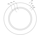
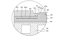
本発明の好適な実施形態を、図面を参照しながら以下に説明する。図1は半導体製造装置用部材10の縦断面図(半導体製造装置用部材10の中心軸を含む面で切断したときの断面図)、図2は半導体製造装置用部材10の平面図、図3は図1の部分拡大図(図1の円で囲まれた部分の拡大図)である。以下の説明において、上下、左右、前後などを用いて説明することがあるが、上下、左右、前後は、相対的な位置関係に過ぎない。
A preferred embodiment of the present invention will be described below with reference to the drawings. Fig. 1 is a vertical cross-sectional view of a semiconductor manufacturing equipment component 10 (a cross-sectional view when cut along a plane including the central axis of the semiconductor manufacturing equipment component 10), Fig. 2 is a plan view of the semiconductor
半導体製造装置用部材10は、ウエハWにプラズマを利用してCVDやエッチングなどを行うために用いられるものであり、半導体プロセス用のチャンバ80の内部に設けられた設置板84に固定されている。半導体製造装置用部材10は、セラミックプレート20と、冷却プレート30と、接合層40と、フォーカスリング60とを備えている。以下、「フォーカスリング」は「FR」と略す。
The semiconductor
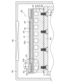
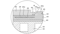
セラミックプレート20は、円形のウエハ載置面22aと、ウエハ載置面22aの外周でウエハ載置面22aよりも一段低い位置に設けられた環状のFR載置面24aとを有する。ウエハ載置面22aには、ウエハWが載置され、FR載置面24aには、FR60が載置される。セラミックプレート20は、アルミナ、窒化アルミニウムなどに代表されるセラミック材料で形成されている。セラミックプレート20は、扁平な円柱部24の上面に円錐台部22を積み上げた形状に形成されている。セラミックプレート20のうち、円錐台部22の上面がウエハ載置面22aであり、円柱部24の上面のうち円錐台部22を除いた環状面がFR載置面24aである。円錐台部22は、ウエハ載置面22aとFR載置面24aとを繋ぐ連結部でもある。そのため、連結部は、ウエハ載置面22aからFR載置面24aに向かって直径が大きくなる円錐台の側面(テーパ面23a)を有する。FR載置面24aに対するテーパ面23aの角度α(図3参照)は、90°未満であればよく、80°以下が好ましく、70°以下がより好ましい。角度αの下限については、特に制限はないが、角度αは20°以上であることが好ましい。角度αが20°以上であれば、FR60の先端部が鋭角になりすぎることがなく、FR60の割れなどの懸念が低減されるため好ましい。ウエハ載置面22aの直径は、ウエハWの直径(例えば300mm)よりも小さい。
The
セラミックプレート20の円錐台部22は、ウエハ吸着用電極25を内蔵している。ウエハ吸着用電極25は、例えばW、Mo、WC、MoCなどを含有する材料によって形成されている。ウエハ吸着用電極25は、円板状又はメッシュ状の単極型の静電電極である。セラミックプレート20のうちウエハ吸着用電極25よりも上側の層は誘電体層として機能する。ウエハ吸着用電極25には、図示しないウエハ吸着用直流電源が接続されている。
The conical
セラミックプレート20の円柱部24は、FR吸着用電極26を内蔵している。FR吸着用電極26は、円柱部24のうちFR載置面24aに対向する位置に埋設されている。FR吸着用電極26は、例えばW、Mo、WC、MoCなどを含有する材料によって形成されている。FR吸着用電極26は、環状又はメッシュ状の単極型の静電電極である。セラミックプレート20のうちFR吸着用電極26よりも上側の層は誘電体層として機能する。FR吸着用電極26には、図示しないFR吸着用直流電源が接続されている。
The
冷却プレート30は、内部に冷媒が循環可能な冷媒流路32を備えた円板部材である。冷媒流路32は、平面視でセラミックプレート20の全面に行き渡るように、一端から他端まで一筆書きの要領で形成されている。本実施形態では、冷却プレート30の直径は、セラミックプレート20の下面の直径と同じである。冷媒流路32を流れる冷媒は、液体が好ましく、電気絶縁性であることが好ましい。電気絶縁性の液体としては、例えばフッ素系不活性液体などが挙げられる。冷却プレート30は、例えば金属を含有する導電材料で作製されている。導電材料としては、例えば、金属や複合材料などが挙げられる。金属としては、Al,Ti,Mo又はそれらの合金などが挙げられる。複合材料としては、金属マトリックス複合材料(メタル・マトリックス・コンポジット(MMC))やセラミックマトリックス複合材料(セラミック・マトリックス・コンポジット(CMC))などが挙げられる。こうした複合材料の具体例としては、Si,SiC及びTiを含む材料やSiC多孔質体にAl及び/又はSiを含浸させた材料などが挙げられる。Si,SiC及びTiを含む材料をSiSiCTiといい、SiC多孔質体にAlを含浸させた材料をAlSiCといい、SiC多孔質体にSiを含浸させた材料をSiSiCという。冷却プレート30の材料としては、セラミックプレート20の材料と熱膨張係数の近いものを選択するのが好ましい。冷却プレート30は、RF電極としても用いられる。冷却プレート30の外周面には、絶縁材料(例えばアルミナやイットリア)で形成された保護膜が形成されていてもよい。
The cooling
接合層40は、セラミックプレート20の下面と冷却プレート30の上面とを接合している。本実施形態では、接合層40は、有機接着層である。有機接着層としては、アクリル樹脂、シリコーン樹脂、エポキシ樹脂等の樹脂を用いることができる。また、樹脂に加えて、フィラーを含有させてもよい。
The
FR60は、FR載置面24aに載置される環状部材であり、例えばシリコンで形成されている。FR60の内周面の上部には、円周方向に沿って段差62が設けられている。段差62は、ウエハWがFR60と干渉するのを防止するために設けられている。FR60の内周面のうちテーパ面23aと対向する部分63は、上方から下方に向かって直径が大きくなる円錐台の側面(テーパ面)である。この部分63は、テーパ面23aとは接触していない。つまり、この部分63とテーパ面23aとの間には隙間が形成されている。そのため、FR60は、セラミックプレート20の円錐台部22の熱的影響を受けにくい。本実施形態では、FR載置面24aに対する部分63の角度β(図3参照)は、FR載置面24aに対するテーパ面23aの角度αと同じである。
FR60 is an annular member placed on the
次に、半導体製造装置用部材10の使用例について図1を用いて説明する。チャンバ80は、天井面にシャワーヘッド82を有する。チャンバ80の内部に配置された設置板84には、半導体製造装置用部材10が固定される。具体的には、半導体製造装置用部材10は、冷却プレート30の下面と設置板84の上面との間に冷却プレート30の直径とほぼ同じ直径を有するOリング88を配置し、その状態で設置板84と冷却プレート30とを複数のボルト90で締結することにより、設置板84に固定される。ボルト90は、頭部と足部とを備える。ボルト90は、設置板84を上下方向に貫通する段差付きのボルト挿通孔86に下方から挿通され、足部が冷却プレート30の下面に設けられたネジ穴34に螺合される。このとき、ボルト90の頭部は、ボルト挿通孔86の段差部に係合する。Oリング88は、上下方向に押し潰されてシール性を発揮する。その他にシール性が必要な箇所があれば、その箇所にも別途Oリングを配置する。
Next, an example of the use of the semiconductor
半導体製造装置用部材10のFR載置面24aには、FR60が載置され、ウエハ載置面22aには、円盤状のウエハWが載置される。この状態で、ウエハ吸着用電極25に直流電圧を印加してウエハWをウエハ載置面22aに吸着させると共に、FR吸着用電極26に直流電圧を印加してFR60をFR載置面24aに吸着させる。そして、チャンバ80の内部を所定の真空雰囲気(又は減圧雰囲気)になるように設定し、シャワーヘッド82からプロセスガスを供給しながら、シャワーヘッド82と冷却プレート30との間に高周波電圧を印加する。すると、冷却プレート30とシャワーヘッド82との間でプラズマが発生する。そして、そのプラズマを利用してウエハWに処理を施す。
The
なお、ウエハWがプラズマ処理されるのに伴ってFR60も消耗するが、FR60はウエハWに比べて厚いため、FR60の交換は複数枚のウエハWを処理したあとに行われる。
The
半導体製造装置用部材10を用いてウエハWを処理する場合、ウエハWにはプラズマによる入熱があるが、ウエハWは冷却プレート30によって冷却される。ウエハWの外周部は、ウエハWの直径がウエハ載置面22aの直径よりも大きいため、ウエハ載置面22aからオーバーハングした状態となっている。そのため、ウエハWの外周部は、冷却プレート30によって熱を奪われにくく、高温になりやすい。しかしながら、本実施形態では、ウエハ載置面22aとFR載置面24aとを繋ぐ連結部(円錐台部22)は、ウエハ載置面22aからFR載置面24aに向かって直径が大きくなる円錐台の側面(テーパ面23a)を有する。そのため、連結部の側面がウエハ載置面22aに対して垂直な場合に比べて、ウエハ載置面22aの外周部から冷却プレート30に向かう熱的なパスが増える。
When the semiconductor
この点を以下に詳説する。図4は、比較形態(特許文献1に開示された従来技術の形態)の部分拡大図である。図4では、セラミックプレート20は、扁平な円柱部24の上面に扁平で小径の円柱部122を積み上げた形状に形成されている。セラミックプレート20のうち、円柱部122の上面がウエハ載置面22aである。円柱部122は、ウエハ載置面22aとFR載置面24aとを繋ぐ連結部でもある。連結部は、円柱部122の側面(垂直面123a)を有する。また、FR60の内周面のうち垂直面123aに対向する部分163も、垂直面となっている。なお、図4では本実施形態と同じ構成要素には同じ符号を付した。図4には、本実施形態のテーパ面23a及び部分63を点線で示した。本実施形態では、連結部(円錐台部22)がウエハ載置面22aからFR載置面24aに向かって直径が大きくなる円錐台の側面(テーパ面23a)を有するため、比較形態のように連結部(円柱部122)が垂直な側面(垂直面123a)を有する場合に比べて、ウエハ載置面22aの外周部から冷却プレート30に向かう熱的なパスが増える。具体的には、図4においてドットハッチングで示す断面直角三角形の領域が増加したパスになる。これにより、本実施形態では、ウエハWのオーバーハングした外周部は、比較形態と比べて抜熱されやすくなる。
This point will be described in detail below. FIG. 4 is a partially enlarged view of a comparative embodiment (the embodiment of the prior art disclosed in Patent Document 1). In FIG. 4, the
また、ウエハ載置面22aに載置されたウエハWは、FR60の内周部を上から覆い被さるように配置されている。この場合、図4の比較形態では、ウエハWによって覆い被さられているFR60の内周部は、プラズマの入熱がウエハWによって遮られるため他の部分よりも冷えやすい。しかしながら、本実施形態では、ウエハWによって覆い被さられるFR60の内周部は、比較形態のFR60の内周部の一部を斜めに切り落とした形状になっているため、冷却プレート30による熱引きが小さい。その結果、一般的に冷えやすいFR60の内周部が過剰に冷えすぎてしまうのを抑制することができる。
The wafer W placed on the
以上説明した半導体製造装置用部材10によれば、連結部(円錐台部22)はウエハ載置面22aからFR載置面24aに向かって直径が大きくなる円錐台の側面を有するため、連結部が垂直な側面(垂直面123a)を有する図4の比較形態に比べて、ウエハ載置面22aの外周部から冷却プレート30に向かう熱的なパスが増える。したがって、ウエハWの外周部を冷却する能力が向上する。
According to the semiconductor
また、ウエハ載置面22aの直径は、載置されるウエハWの直径よりも小さい。この場合、ウエハWの外周部は特に高温になりやすいため、本発明を適用する意義が高い。
The diameter of the
更に、FR載置面24a対するテーパ面23aの角度αは、70°以下であることが好ましい。こうすれば、ウエハ載置面22aの外周部から冷却プレート30に向かう熱的なパスを十分増やすことができる。
Furthermore, it is preferable that the angle α of the tapered
更にまた、FR60の内周面のうちテーパ面23aと対向する部分63は、上方から下方に向かって直径が大きくなる円錐台の側面である。そのため、一般的に冷えやすいFR60の内周部が過剰に冷えすぎてしまうのを抑制することができる。
Furthermore, the
そしてまた、セラミックプレート20の連結部(円錐台部22)の側面もFR60の内周面の部分63もテーパ面であるため、FR60をFR載置面24aに載置する際、セルフアライメント効果によりFR60の設置位置精度が向上する。
Furthermore, because both the side of the connecting portion (frustum portion 22) of the
なお、本発明は上述した実施形態に何ら限定されることはなく、本発明の技術的範囲に属する限り種々の態様で実施し得ることはいうまでもない。 It goes without saying that the present invention is in no way limited to the above-described embodiment, and can be implemented in various forms as long as they fall within the technical scope of the present invention.
上述した実施形態では、FR載置面24aに対するテーパ面23aの角度αとFR載置面24aに対する部分63(テーパ面)の角度βとを同じにしたが、特にこれに限定されず、例えば図5や図6の構成を採用してもよい。図5及び図6では、上述した実施形態と同じ構成要素には同じ符号を付した。
In the embodiment described above, the angle α of the tapered
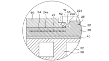
図5では、FR載置面24aに対する部分63(テーパ面)の角度βは、FR載置面24aに対するテーパ面23aの角度αよりも大きい(つまりβ>α)。こうすれば、FR60の部分63(テーパ面)とセラミックプレート20のテーパ面23aとの隙間は上に行くほど広がるため、FR60の部分63(テーパ面)がセラミックプレート20に接触するのを防止しやすくなる。
In Figure 5, the angle β of portion 63 (tapered surface) relative to
図6では、FR載置面24aに対する部分63(テーパ面)の角度βは、FR載置面24aに対するテーパ面23aの角度αよりも小さい(つまりβ<α)。こうすれば、FR60の内周部側の下面とFR載置面24aとの接触面積を十分小さくすることができるため、一般的に冷えやすいFR60の内周部が過剰に冷えすぎてしまうのをより効果的に抑制することができる。
In FIG. 6, the angle β of portion 63 (tapered surface) relative to
図5及び図6において、これらα、βの角度差は30°以下が好ましく、15°以下がより好ましい。こうすれば、FR60の部分63とセラミックプレート20のテーパ面23aとの間の空間が大きくなりすぎて放電といった別の問題が生じる懸念を低減することができる。
In Figures 5 and 6, the difference between the angles α and β is preferably 30° or less, and more preferably 15° or less. This reduces the risk of the space between the
上述した実施形態では、セラミックプレート20のテーパ面23aやFR60の内周面のうちテーパ面23aと対向する部分63を、厳密に円錐台の側面としたが、特にこれに限定されない。例えば、厳密な円錐台の側面の代わりに、円錐台の側面が凸に膨らんだ形状を採用してもよいし、凹にへこんだ形状を採用してもよい。部分63についても、これと同様である。
In the above-described embodiment, the
上述した実施形態において、セラミックプレート20の円錐台部22にウエハ加熱用ヒータ電極を埋設してもよい。こうすれば、ウエハ載置面22aに載置されるウエハWを高温にする必要がある場合に、ウエハ加熱用ヒータ電極に通電してウエハWを所望の高温にすることができる。また、セラミックプレート20の円柱部24のうちFR載置面24aに対向する位置にFR加熱用ヒータ電極を埋設してもよい。こうすれば、FR載置面24aに載置されるFR60を高温にする必要がある場合に、FR加熱用ヒータ電極に通電してFR60を所望の高温にすることができる。セラミックプレート20にウエハ加熱用ヒータ電極とFR加熱用ヒータ電極の両方を埋設する場合、それぞれのヒータ電極を個別に温度調整可能にするのが好ましい。
In the above-described embodiment, a heater electrode for heating the wafer may be embedded in the
上述した実施形態では、接合層40として有機接着層を採用したが、特にこれに限定されない。例えば、接合層40は、金属などの無機接合層としてもよい。無機接合層は、はんだや金属ロウ材(例えばアルミニウムやチタンなどのロウ材)で形成された金属接合層であってもよい。金属接合層は、例えばTCB(Thermal compression bonding)により形成されていてもよい。TCBとは、接合対象の2つの部材の間に金属接合材を挟み込み、金属接合材の固相線温度以下の温度に加熱した状態で2つの部材を加圧接合する公知の方法をいう。
In the above-described embodiment, an organic adhesive layer is used as the
本発明は、半導体製造装置に用いられる部材、例えば静電チャックヒータ、静電チャック、セラミックヒータなどに利用可能である。 The present invention can be used in components used in semiconductor manufacturing equipment, such as electrostatic chuck heaters, electrostatic chucks, and ceramic heaters.
10 半導体製造装置用部材、20 セラミックプレート、22 円錐台部、22a ウエハ載置面、23a テーパ面、24 円柱部、24a FR載置面、25 ウエハ吸着用電極、26 FR吸着用電極、30 冷却プレート、32 冷媒流路、34 ネジ穴、40 接合層、60 フォーカスリング(FR)、62 段差、63 部分、80 チャンバ、82 シャワーヘッド、84 設置板、86 ボルト挿通孔、88 Oリング、90 ボルト、122 円柱部、123a 垂直面、163 部分。 10 Semiconductor manufacturing equipment member, 20 Ceramic plate, 22 Cone frustum, 22a Wafer mounting surface, 23a Tapered surface, 24 Cylindrical portion, 24a FR mounting surface, 25 Wafer suction electrode, 26 FR suction electrode, 30 Cooling plate, 32 Coolant flow path, 34 Screw hole, 40 Bonding layer, 60 Focus ring (FR), 62 Step, 63 Part, 80 Chamber, 82 Shower head, 84 Installation plate, 86 Bolt insertion hole, 88 O-ring, 90 Bolt, 122 Cylindrical portion, 123a Vertical surface, 163 Part.
Claims (6)
前記セラミックプレートの下面に設けられた冷却プレートと、
を備え、
前記ウエハ載置面と前記フォーカスリング載置面とを繋ぐ連結部は、前記ウエハ載置面から前記フォーカスリング載置面に向かって直径が大きくなる円錐台の側面を有する、
半導体製造装置用部材。 a ceramic plate having a circular wafer mounting surface and an annular focus ring mounting surface provided at an outer periphery of the wafer mounting surface and one step lower than the wafer mounting surface;
a cooling plate provided on a lower surface of the ceramic plate;
Equipped with
a connecting portion connecting the wafer mounting surface and the focus ring mounting surface has a side surface of a truncated cone whose diameter increases from the wafer mounting surface toward the focus ring mounting surface.
Components for semiconductor manufacturing equipment.
請求項1に記載の半導体製造装置用部材。 The diameter of the wafer mounting surface is smaller than the diameter of the wafer to be mounted.
The semiconductor manufacturing equipment member according to claim 1 .
請求項1又は2に記載の半導体製造装置用部材。 an angle of the side surface of the coupling portion with respect to the focus ring mounting surface is equal to or smaller than 70°;
The semiconductor manufacturing equipment member according to claim 1 or 2.
前記フォーカスリング載置面に載置されるフォーカスリング
を備え、
前記フォーカスリングの内周面のうち前記連結部の側面と対向する部分は、上方から下方に向かって直径が大きくなる円錐台の側面である、
半導体製造装置用部材。 The semiconductor manufacturing equipment member according to claim 1 or 2,
a focus ring mounted on the focus ring mounting surface,
a portion of an inner circumferential surface of the focus ring facing the side surface of the connecting portion is a side surface of a truncated cone whose diameter increases from above to below;
Components for semiconductor manufacturing equipment.
請求項4に記載の半導体製造装置用部材。 an angle of the portion with respect to the focus ring mounting surface is larger than an angle of a side surface of the coupling portion with respect to the focus ring mounting surface;
The semiconductor manufacturing equipment member according to claim 4 .
請求項4に記載の半導体製造装置用部材。 an angle of the portion with respect to the focus ring mounting surface is smaller than an angle of a side surface of the coupling portion with respect to the focus ring mounting surface;
The semiconductor manufacturing equipment member according to claim 4 .
Priority Applications (8)
| Application Number | Priority Date | Filing Date | Title |
|---|---|---|---|
| CN202380012896.2A CN121753530A (en) | 2023-08-21 | 2023-08-21 | Component for semiconductor manufacturing device |
| JP2024510644A JP7671918B1 (en) | 2023-08-21 | 2023-08-21 | Semiconductor manufacturing equipment parts |
| KR1020267006364A KR20260038955A (en) | 2023-08-21 | 2023-08-21 | Member for semiconductor manufacturing device |
| KR1020247008757A KR102934502B1 (en) | 2023-08-21 | 2023-08-21 | Components for semiconductor manufacturing equipment |
| PCT/JP2023/029982 WO2025041221A1 (en) | 2023-08-21 | 2023-08-21 | Member for semiconductor manufacturing device |
| US18/584,006 US12463023B2 (en) | 2023-08-21 | 2024-02-22 | Member for semiconductor manufacturing apparatus |
| TW113114105A TW202510091A (en) | 2023-08-21 | 2024-04-16 | Parts for semiconductor manufacturing equipment |
| US19/332,181 US20260018393A1 (en) | 2023-08-21 | 2025-09-18 | Member for semiconductor manufacturing apparatus |
Applications Claiming Priority (1)
| Application Number | Priority Date | Filing Date | Title |
|---|---|---|---|
| PCT/JP2023/029982 WO2025041221A1 (en) | 2023-08-21 | 2023-08-21 | Member for semiconductor manufacturing device |
Related Child Applications (1)
| Application Number | Title | Priority Date | Filing Date |
|---|---|---|---|
| US18/584,006 Continuation US12463023B2 (en) | 2023-08-21 | 2024-02-22 | Member for semiconductor manufacturing apparatus |
Publications (1)
| Publication Number | Publication Date |
|---|---|
| WO2025041221A1 true WO2025041221A1 (en) | 2025-02-27 |
Family
ID=94689171
Family Applications (1)
| Application Number | Title | Priority Date | Filing Date |
|---|---|---|---|
| PCT/JP2023/029982 Pending WO2025041221A1 (en) | 2023-08-21 | 2023-08-21 | Member for semiconductor manufacturing device |
Country Status (6)
| Country | Link |
|---|---|
| US (2) | US12463023B2 (en) |
| JP (1) | JP7671918B1 (en) |
| KR (2) | KR102934502B1 (en) |
| CN (1) | CN121753530A (en) |
| TW (1) | TW202510091A (en) |
| WO (1) | WO2025041221A1 (en) |
Citations (10)
| Publication number | Priority date | Publication date | Assignee | Title |
|---|---|---|---|---|
| JPH07106316A (en) * | 1993-10-04 | 1995-04-21 | Tokyo Electron Ltd | Plasma processing device |
| JP2000173988A (en) * | 1998-12-01 | 2000-06-23 | Sumitomo Metal Ind Ltd | Substrate holder and plasma processing device |
| JP2002093894A (en) * | 2000-06-19 | 2002-03-29 | Applied Materials Inc | Ceramic substrate support |
| JP2009152232A (en) * | 2007-12-18 | 2009-07-09 | Mitsubishi Materials Corp | Composite silicon ring for plasma etching equipment to support wafer |
| JP2013512564A (en) * | 2009-11-30 | 2013-04-11 | ラム リサーチ コーポレーション | Electrostatic chuck with inclined side walls |
| JP2016195108A (en) * | 2015-03-31 | 2016-11-17 | ラム リサーチ コーポレーションLam Research Corporation | Plasma processing system and plasma processing structure having an inclined confinement ring |
| JP2016207979A (en) * | 2015-04-28 | 2016-12-08 | 日本特殊陶業株式会社 | Electrostatic chuck |
| JP2018107433A (en) * | 2016-12-27 | 2018-07-05 | 東京エレクトロン株式会社 | Focus ring and substrate processing apparatus |
| JP2019169699A (en) * | 2018-03-22 | 2019-10-03 | Sppテクノロジーズ株式会社 | Focus ring and plasma processing apparatus including the same |
| JP2023027641A (en) * | 2021-08-17 | 2023-03-02 | 日本碍子株式会社 | Wafer table |
Family Cites Families (5)
| Publication number | Priority date | Publication date | Assignee | Title |
|---|---|---|---|---|
| US5529657A (en) | 1993-10-04 | 1996-06-25 | Tokyo Electron Limited | Plasma processing apparatus |
| KR100292410B1 (en) * | 1998-09-23 | 2001-06-01 | 윤종용 | Process chamber for reducing particulate contamination for manufacturing semiconductor device |
| US20180182635A1 (en) | 2016-12-27 | 2018-06-28 | Tokyo Electron Limited | Focus ring and substrate processing apparatus |
| JP2024516149A (en) * | 2021-04-21 | 2024-04-12 | ラム リサーチ コーポレーション | Prevents backside deposition on substrate |
| KR102904705B1 (en) * | 2021-11-09 | 2025-12-29 | 삼성전자주식회사 | Focus ring, apparatus for substrate treatment including the same and method for substrate treatment using the same |
-
2023
- 2023-08-21 KR KR1020247008757A patent/KR102934502B1/en active Active
- 2023-08-21 KR KR1020267006364A patent/KR20260038955A/en active Pending
- 2023-08-21 JP JP2024510644A patent/JP7671918B1/en active Active
- 2023-08-21 CN CN202380012896.2A patent/CN121753530A/en active Pending
- 2023-08-21 WO PCT/JP2023/029982 patent/WO2025041221A1/en active Pending
-
2024
- 2024-02-22 US US18/584,006 patent/US12463023B2/en active Active
- 2024-04-16 TW TW113114105A patent/TW202510091A/en unknown
-
2025
- 2025-09-18 US US19/332,181 patent/US20260018393A1/en active Pending
Patent Citations (10)
| Publication number | Priority date | Publication date | Assignee | Title |
|---|---|---|---|---|
| JPH07106316A (en) * | 1993-10-04 | 1995-04-21 | Tokyo Electron Ltd | Plasma processing device |
| JP2000173988A (en) * | 1998-12-01 | 2000-06-23 | Sumitomo Metal Ind Ltd | Substrate holder and plasma processing device |
| JP2002093894A (en) * | 2000-06-19 | 2002-03-29 | Applied Materials Inc | Ceramic substrate support |
| JP2009152232A (en) * | 2007-12-18 | 2009-07-09 | Mitsubishi Materials Corp | Composite silicon ring for plasma etching equipment to support wafer |
| JP2013512564A (en) * | 2009-11-30 | 2013-04-11 | ラム リサーチ コーポレーション | Electrostatic chuck with inclined side walls |
| JP2016195108A (en) * | 2015-03-31 | 2016-11-17 | ラム リサーチ コーポレーションLam Research Corporation | Plasma processing system and plasma processing structure having an inclined confinement ring |
| JP2016207979A (en) * | 2015-04-28 | 2016-12-08 | 日本特殊陶業株式会社 | Electrostatic chuck |
| JP2018107433A (en) * | 2016-12-27 | 2018-07-05 | 東京エレクトロン株式会社 | Focus ring and substrate processing apparatus |
| JP2019169699A (en) * | 2018-03-22 | 2019-10-03 | Sppテクノロジーズ株式会社 | Focus ring and plasma processing apparatus including the same |
| JP2023027641A (en) * | 2021-08-17 | 2023-03-02 | 日本碍子株式会社 | Wafer table |
Also Published As
| Publication number | Publication date |
|---|---|
| US12463023B2 (en) | 2025-11-04 |
| JPWO2025041221A1 (en) | 2025-02-27 |
| JP7671918B1 (en) | 2025-05-02 |
| KR20250029010A (en) | 2025-03-04 |
| US20250069865A1 (en) | 2025-02-27 |
| CN121753530A (en) | 2026-03-27 |
| US20260018393A1 (en) | 2026-01-15 |
| KR102934502B1 (en) | 2026-03-06 |
| KR20260038955A (en) | 2026-03-19 |
| TW202510091A (en) | 2025-03-01 |
Similar Documents
| Publication | Publication Date | Title |
|---|---|---|
| US20230146815A1 (en) | Wafer placement table | |
| KR102800130B1 (en) | Wafer placement table | |
| KR20230053499A (en) | Wafer placement table | |
| KR20240046104A (en) | wafer placement table | |
| US12543527B2 (en) | Wafer placement table, and member for semiconductor manufacturing apparatus, using the same | |
| JP7714505B2 (en) | Wafer mounting table and semiconductor manufacturing equipment component using the same | |
| JP7671918B1 (en) | Semiconductor manufacturing equipment parts | |
| CN119365972A (en) | Wafer loading platform | |
| JP7751079B2 (en) | Semiconductor manufacturing equipment components | |
| KR102875929B1 (en) | Wafer placement table | |
| US12537174B2 (en) | Wafer placement table | |
| JP7503708B1 (en) | Semiconductor manufacturing equipment parts | |
| US20230144107A1 (en) | Wafer placement table | |
| JP7705456B2 (en) | Semiconductor manufacturing equipment parts | |
| KR102718069B1 (en) | Wafer placement table | |
| JP7515018B1 (en) | Semiconductor manufacturing equipment parts | |
| KR102817676B1 (en) | Wafer placement table | |
| US20260128263A1 (en) | Wafer placement table | |
| KR102846887B1 (en) | Wafer placement table | |
| KR20260057568A (en) | component for semiconductor manufacturing equipment | |
| CN116564779A (en) | Wafer stage and component for semiconductor manufacturing equipment using the same |
Legal Events
| Date | Code | Title | Description |
|---|---|---|---|
| ENP | Entry into the national phase |
Ref document number: 2024510644 Country of ref document: JP Kind code of ref document: A |
|
| WWE | Wipo information: entry into national phase |
Ref document number: 2024510644 Country of ref document: JP |
|
| WWP | Wipo information: published in national office |
Ref document number: 1020247008757 Country of ref document: KR |
|
| 121 | Ep: the epo has been informed by wipo that ep was designated in this application |
Ref document number: 23949682 Country of ref document: EP Kind code of ref document: A1 |
|
| NENP | Non-entry into the national phase |
Ref country code: DE |