WO2025037413A1 - 位相調整器及び半導体光集積素子 - Google Patents
位相調整器及び半導体光集積素子 Download PDFInfo
- Publication number
- WO2025037413A1 WO2025037413A1 PCT/JP2023/029654 JP2023029654W WO2025037413A1 WO 2025037413 A1 WO2025037413 A1 WO 2025037413A1 JP 2023029654 W JP2023029654 W JP 2023029654W WO 2025037413 A1 WO2025037413 A1 WO 2025037413A1
- Authority
- WO
- WIPO (PCT)
- Prior art keywords
- optical
- phase adjustment
- electrode
- optical waveguide
- phase
- Prior art date
- Legal status (The legal status is an assumption and is not a legal conclusion. Google has not performed a legal analysis and makes no representation as to the accuracy of the status listed.)
- Pending
Links
Images


Classifications
-
- G—PHYSICS
- G02—OPTICS
- G02F—OPTICAL DEVICES OR ARRANGEMENTS FOR THE CONTROL OF LIGHT BY MODIFICATION OF THE OPTICAL PROPERTIES OF THE MEDIA OF THE ELEMENTS INVOLVED THEREIN; NON-LINEAR OPTICS; FREQUENCY-CHANGING OF LIGHT; OPTICAL LOGIC ELEMENTS; OPTICAL ANALOGUE/DIGITAL CONVERTERS
- G02F1/00—Devices or arrangements for the control of the intensity, colour, phase, polarisation or direction of light arriving from an independent light source, e.g. switching, gating or modulating; Non-linear optics
- G02F1/01—Devices or arrangements for the control of the intensity, colour, phase, polarisation or direction of light arriving from an independent light source, e.g. switching, gating or modulating; Non-linear optics for the control of the intensity, phase, polarisation or colour
- G02F1/015—Devices or arrangements for the control of the intensity, colour, phase, polarisation or direction of light arriving from an independent light source, e.g. switching, gating or modulating; Non-linear optics for the control of the intensity, phase, polarisation or colour based on semiconductor elements having potential barriers, e.g. having a PN or PIN junction
- G02F1/025—Devices or arrangements for the control of the intensity, colour, phase, polarisation or direction of light arriving from an independent light source, e.g. switching, gating or modulating; Non-linear optics for the control of the intensity, phase, polarisation or colour based on semiconductor elements having potential barriers, e.g. having a PN or PIN junction in an optical waveguide structure
Definitions
- This disclosure relates to a phase adjuster and a semiconductor optical integrated device.
- Patent documents 1 to 3 disclose phase adjusters that change the phase of signal light propagating through an optical waveguide using a method of applying a reverse bias voltage to a diode provided in the optical waveguide, a method of applying a forward bias voltage to a diode provided in the optical waveguide to pass a current, and a method of passing a current through a heater electrode provided around the optical waveguide to change the temperature of the optical waveguide.
- the method of adjusting the phase using a heater has the advantage that it is easy to control because the amount of phase change obtained is roughly proportional to the applied power, but it has issues such as the difficulty of adjusting the optical loss and the need to apply a relatively large amount of power to the heater electrode.
- the method of applying a forward bias voltage to pass a current has intermediate characteristics between the two methods mentioned above and is relatively easy to control.
- the present disclosure has been made to solve the problems described above, and aims to provide a compact phase adjuster that is capable of adjusting the amount of loss and phase change of an optical signal propagating through an optical waveguide, and a semiconductor optical integrated device in which such a phase adjuster is integrated on a semiconductor substrate.
- the phase adjuster includes: a first optical waveguide portion having a striped ridge structure including a lower cladding layer, an optical waveguide core layer, and an upper cladding layer laminated on a surface of a semiconductor substrate; a phase adjustment portion having the ridge structure and provided in contact with the first optical waveguide portion in a stripe direction; a second optical waveguide portion having the ridge structure and provided in contact with the phase adjustment portion in the stripe direction; an upper phase adjustment electrode provided on the top of the ridge structure of the phase adjustment portion and extending along the stripe direction; a lower phase adjustment electrode electrically connected to the lower cladding layer; a first extraction electrode electrically connected to the upper phase adjustment electrode; a second extraction electrode electrically connected to the upper phase adjustment electrode; Equipped with.
- the semiconductor optical integrated device comprises: an optical demultiplexer that branches an incident signal light into a plurality of optical waveguides; a plurality of optical modulators, one end of each of which is connected to the plurality of optical waveguides; the phase adjuster, one end of which is connected to the other end of each of the optical modulators via the optical waveguide; an optical multiplexer/demultiplexer connected to the other ends of the plurality of phase adjusters via the optical waveguide; Equipped with.
- the phase adjuster disclosed herein has the advantage that it is possible to adjust the amount of loss and the amount of phase change of an optical signal propagating through an optical waveguide, and that a compact phase adjuster can be obtained.
- the semiconductor optical integrated device has the advantage that it is possible to adjust the amount of loss and the amount of phase change of an optical signal propagating through an optical waveguide, and that a semiconductor optical integrated device is obtained in which a miniaturized phase adjuster is integrated on a semiconductor substrate.
- FIG. 2 is a cross-sectional view of the phase adjuster according to the first embodiment in a direction parallel to the propagation direction of signal light.
- FIG. 2 is a top view of the phase adjuster according to the first embodiment.
- 3 is a cross-sectional view of the phase adjuster according to the first embodiment in a direction perpendicular to the propagation direction of signal light in the optical waveguide portion.
- 4 is a cross-sectional view of a phase adjustment unit of the phase adjuster according to the first embodiment in a direction perpendicular to the propagation direction of signal light.
- 11 is a cross-sectional view of a phase adjuster according to a second embodiment in a direction parallel to the propagation direction of signal light.
- FIG. 11 is a cross-sectional view of a phase adjuster according to a third embodiment in a direction parallel to the propagation direction of signal light.
- FIG. 11 is a top view of a phase adjuster according to a third embodiment.
- FIG. 13 is a top view of a semiconductor optical integrated device according to a fourth embodiment. 13 is a cross-sectional view in a direction parallel to the propagation direction of signal light in an optical modulator of a semiconductor optical integrated device according to a fourth embodiment. 13 is a cross-sectional view taken along a direction perpendicular to the propagation direction of signal light in an optical modulator of a semiconductor optical integrated device according to a fourth embodiment.
- Fig. 1 is a cross-sectional view of a phase adjuster 500, which is an example of the phase adjuster according to the first embodiment, in a direction parallel to the propagation direction of signal light.
- Fig. 2 is a top view of the phase adjuster 500, which is an example of the phase adjuster according to the first embodiment.
- the phase adjuster 500 includes, on a semiconductor substrate 100, a first optical waveguide portion 10a, a phase adjuster portion 20 provided in contact with the first optical waveguide portion 10a in the stripe direction, and a second optical waveguide portion 10b provided in contact with the phase adjuster portion 20 in the stripe direction.
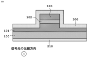
- FIG. 3 is a cross-sectional view of the first optical waveguide section 10a and the second optical waveguide section 10b of the phase adjuster 500 according to the first embodiment in a direction perpendicular to the propagation direction of the signal light.
- the first optical waveguide section 10a and the second optical waveguide section 10b have a striped ridge structure including a lower cladding layer 101, an optical waveguide core layer 102, and an upper cladding layer 103, which are sequentially stacked on the surface of the semiconductor substrate 100.
- the refractive index of the material constituting the optical waveguide core layer 102 is greater than the refractive index of the material constituting the lower cladding layer 101 and the refractive index of the material constituting the upper cladding layer 103. Due to the difference in refractive index between the optical waveguide core layer 102 and the refractive index of the lower cladding layer 101 and the upper cladding layer 103, the signal light input to the phase adjuster 500 can be confined vertically within the optical waveguide core layer 102 and propagated to the optical output side.
- the first optical waveguide section 10a and the second optical waveguide section 10b have a striped ridge structure in the horizontal direction relative to the surface of the semiconductor substrate 100.
- a protective insulating film 300 with a smaller refractive index than the optical waveguide core layer 102 so as to cover this ridge structure, the input signal light can be confined in the optical waveguide core layer 102 in the horizontal direction relative to the surface of the semiconductor substrate 100 due to the refractive index difference described above, and propagated to the optical output side.
- phase adjustment unit 20 has a striped ridge structure including a lower cladding layer 201, an optical waveguide core layer 202, and an upper cladding layer 203, which are sequentially stacked on the surface of the semiconductor substrate 100.
- an upper phase adjustment electrode 211 electrically connected to the upper clad layer 203 is formed on the surface of the upper clad layer 203 of the phase adjustment section 20.
- a lower phase adjustment electrode 210 is formed on the back surface of the semiconductor substrate 100.
- the lower phase adjustment electrode 210 is electrically connected to the lower clad layer 201. Note that in FIG. 3, the lower phase adjustment electrode 210 is electrically connected to the lower clad layer 201 via the semiconductor substrate 100, but the lower phase adjustment electrode 210 may be formed on the lower clad layer 201, for example, and disposed so that the lower phase adjustment electrode 210 is directly and electrically connected to the lower clad layer 201.
- both of the above-mentioned connection modes of the lower phase adjustment electrode 210 are expressed as the lower phase adjustment electrode 210 being electrically connected to the lower clad layer 201.
- the optical waveguide core layer 102 of the first optical waveguide section 10a and the second optical waveguide section 10b is not actually visible from the top side, but for convenience of explanation, the internal position is illustrated as the optical waveguide core layer 102a.
- the lower cladding layer 101 of the first optical waveguide section 10a and the second optical waveguide section 10b and the lower cladding layer 201 of the phase adjustment section 20 may be a single continuous semiconductor layer as a crystal growth layer, or may be different semiconductor layers.
- the optical waveguide core layer 102 and the upper cladding layer 103 of the first optical waveguide section 10a and the second optical waveguide section 10b, and the optical waveguide core layer 202 and the upper cladding layer 203 of the phase adjustment section 20 may also be a single continuous semiconductor layer as a crystal growth layer, or may be different semiconductor layers.
- the ridge structure may be a common continuous ridge structure in the first optical waveguide section 10a, the phase adjustment section 20, and the second optical waveguide section 10b, or may be different optical waveguide core layer structures.
- the refractive index of the optical waveguide core layer 202 is greater than the refractive index of the lower cladding layer 201 and the refractive index of the upper cladding layer 203. Due to the difference in refractive index between the optical waveguide core layer 202 and the refractive index of the lower cladding layer 201 and the upper cladding layer 203, the input signal light can be confined vertically within the optical waveguide core layer 202 and propagated to the optical output side.
- the phase adjustment section 20 has a striped ridge structure.
- a protective insulating film 300 with a smaller refractive index than the optical waveguide core layer 202 so as to cover this ridge structure, the input signal light can be confined horizontally to the surface of the semiconductor substrate 100 within the optical waveguide core layer 202 due to the refractive index difference described above, and propagated to the optical output side.
- the upper phase adjustment electrode 211 provided on the surface of the upper cladding layer 203 exposed at the top of the ridge structure extends along the direction in which the signal light propagates, i.e., the stripe direction.
- a first extraction electrode 220 is electrically connected to one end of the upper phase adjustment electrode 211, i.e., the side where the signal light is input, and a second extraction electrode 221 is connected to the other end of the upper phase adjustment electrode 211, i.e., the side where the signal light is output.
- the first extraction electrode 220 and the second extraction electrode 221 are formed on the protective insulating film 300 except for the portion connected to the upper phase adjustment electrode 211.
- a potential difference is applied between the first extraction electrode 220 and the second extraction electrode 221 by a power supply provided outside the phase adjuster 500.
- a current flows inside the upper phase adjustment electrode 211 along the stripe direction in which the upper phase adjustment electrode 211 extends.
- the upper phase adjustment electrode 211 Since the upper phase adjustment electrode 211 has electrical resistance in the extending stripe direction, when a current flows through the upper phase adjustment electrode 211, Joule heat is generated. In other words, the upper phase adjustment electrode 211 functions as a heater. When the Joule heat generated from the upper phase adjustment electrode 211 is thermally conducted to the optical waveguide core layer 202 via the upper cladding layer 203, the refractive index of the optical waveguide core layer 202 changes due to the thermo-optical effect. In other words, the phase of the signal light propagating through the optical waveguide core layer 202 of the phase adjustment unit 20 can be changed using the thermo-optical effect.
- a potential difference is also applied between the first and second extraction electrodes 220 and 221 and the lower phase adjustment electrode 210 by a power source provided outside the phase adjuster 500.
- a current flows through the lower cladding layer 201, the optical waveguide core layer 202, and the upper cladding layer 203.
- the amount of carriers present in the optical waveguide core layer 202 changes due to the flow of such a current
- the refractive index and amount of optical loss of the optical waveguide core layer 202 change due to the carrier plasma effect.
- the amount of current passing through the lower cladding layer 201, the optical waveguide core layer 202, and the upper cladding layer 203 it is possible to change the phase and amount of optical loss of the signal light propagating through the optical waveguide core layer 202 of the phase adjustment unit 20.
- phase adjuster 500 of the first embodiment it is possible to simultaneously obtain a phase adjustment function by a heater using electrical resistance in the phase adjustment section 20 and a phase and optical loss adjustment function by a current passing through the optical waveguide core layer 202, which makes it possible to realize a miniaturized phase adjuster, and in turn, to miniaturize the semiconductor optical integrated device that integrates such a phase adjuster.
- a contact layer made of a low-resistance semiconductor may be formed between the upper phase adjustment electrode 211 and the upper cladding layer 203.
- a commonly known structure may be added, such as covering the sidewalls of the ridge shape with a semiconductor layer having a lower refractive index than the optical waveguide core layer 202 and then forming the protective insulating film 300.
- phase adjuster 500 a method for manufacturing the phase adjuster 500 according to the first embodiment will be described in detail below.
- an n-type InP (indium phosphide) substrate which is an example of the semiconductor substrate 100
- an n-type InP layer having a thickness of 2.0 ⁇ m is crystal-grown to become the lower cladding layer 101 and the lower cladding layer 201, using an epitaxial crystal growth method such as metal organic chemical vapor deposition (MOCVD).
- MOCVD metal organic chemical vapor deposition
- the composition and thickness of the optical waveguide core layer 102 and the optical waveguide core layer 202 may be appropriately selected according to the wavelength of the input optical signal.
- the wavelength of the optical signal is 1.55 ⁇ m, which is commonly used in optical communications
- an example of an alloy semiconductor that constitutes the optical waveguide core layer 102 and the optical waveguide core layer 202 is an InGaAsP alloy semiconductor with a layer thickness of 400 nm, which has an emission peak wavelength of 1.2 ⁇ m by photoluminescence.
- the optical waveguide core layer 102 and the optical waveguide core layer 202 may have a structure called a multiple quantum well structure, in which layers made of alloy semiconductors with different compositions and a layer thickness of about 10 nm are alternately stacked multiple times. In this case, a steep change in refractive index and change in optical loss can be obtained in the optical waveguide core layer 202 when a bias is applied due to the so-called quantum confined Stark effect.
- a layered structure called an SCH (Separate Confinement Heterostructure) layer may be added above and below the optical waveguide core layer 102 and the optical waveguide core layer 202.
- the layered structure is made of a mixed crystal semiconductor having a higher refractive index than the lower cladding layer 101 and the lower cladding layer 201 and the upper cladding layer 103 and the upper cladding layer 203, and a lower refractive index than the optical waveguide core layer 102 and the optical waveguide core layer 202.
- different optical waveguide core layer structures may be adopted between the first optical waveguide section 10a and the second optical waveguide section 10b and the phase adjustment section 20.
- the optical waveguide core layer may be selectively removed from the regions that will become the first optical waveguide section 10a and the second optical waveguide section 10b by wet etching using a chemical solution or dry etching using plasma of a reactive gas, and an optical waveguide core layer with a different layer structure may be crystal-grown again by MOCVD in the removed regions.
- a SiO 2 film patterned into stripes having a width of 1.0 ⁇ m to 3.0 ⁇ m is formed as a protective mask by photolithography and etching techniques so as to form a desired optical waveguide shape on the surfaces of the upper clad layer 103 and the upper clad layer 203.
- the areas not covered with the SiO 2 film are etched by dry etching or wet etching until the lower clad layer 101 and the lower clad layer 201 are exposed.
- a protective insulating film 300 such as a 500 nm-thick SiO2 film is deposited by plasma CVD or the like.
- the upper part of the ridge structure i.e., the SiO2 film at the top
- the upper cladding layer 203 is exposed on the surface, and a conductive film that becomes the upper phase adjustment electrode 211 is formed.
- the upper phase adjustment electrode 211 needs to have a certain resistance value and function as a heater. Therefore, examples of materials that constitute the upper phase adjustment electrode 211 include metals such as platinum and titanium, alloys such as nichrome, metal nitrides such as tantalum nitride, and metal oxides such as indium tin oxide.
- the upper phase adjustment electrode 211 is made of a thin film with a film thickness of about 200 nm.
- a first extraction electrode 220 is formed in contact with a portion near one end of the upper phase adjustment electrode 211, which is the input side of the optical signal in the phase adjustment section 20, and a second extraction electrode 221 is formed in contact with a portion near the other end of the upper phase adjustment electrode 211, which is the output side of the optical signal.
- Methods for forming the first extraction electrode 220 and the second extraction electrode 221 include vapor deposition, sputtering, plating, etc.
- a low-resistance metal such as gold is used as the material for the first extraction electrode 220 and the second extraction electrode 221.
- One example of the material for the first extraction electrode 220 and the second extraction electrode 221 is gold with a film thickness of 3 ⁇ m.
- the resistance value R1 first resistance value
- the resistance value R1 between the first extraction electrode 220 and the second extraction electrode 221 to be approximately the same as the resistance value R2 (second resistance value) of the semiconductor layer when a forward voltage is applied between the upper phase adjustment electrode 211 and the lower phase adjustment electrode 210.
- the reason for this is that if one resistance value is too low, not enough current flows between the other electrode, and it is not possible to simultaneously obtain both a refractive index change due to the thermo-optical effect and a refractive index change and light loss change due to the carrier plasma effect.
- the ratio of the resistance value R1 between both ends of the upper phase adjustment electrode 211 to the resistance value R2 of the semiconductor layer between the upper phase adjustment electrode 211 and the lower phase adjustment electrode 210 should be 100 or less, preferably 10 or less, and even more preferably about 1.
- an upper phase adjustment electrode having one end connected to the first extraction electrode and the other end connected to the second extraction electrode is provided in the phase adjustment section of the phase adjuster, thereby making it possible to adjust the amount of loss and the amount of phase change of an optical signal propagating through the optical waveguide, and achieving the effect of obtaining a compact phase adjuster.
- Embodiment 2. 5 is a cross-sectional view of the phase adjuster according to the second embodiment in a direction parallel to the propagation direction of the signal light.
- Phase adjuster 600 according to the second embodiment differs from phase adjuster 500 according to the first embodiment in that, as shown in FIG. 5, insulating film 310 is formed in a part of the region between upper phase adjuster electrode 211 and upper clad layer 203 so that the amount of current flowing in upper phase adjuster electrode 211 is not extremely small compared to the amount of current flowing between upper phase adjuster electrode 211 and lower phase adjuster electrode 210.
- a semiconductor layer with low resistance is used, such as by doping the semiconductor layer with a high concentration of impurities or by using a semiconductor layer with high carrier mobility as the semiconductor layer that forms the contact surface.
- the upper phase adjustment electrode 211 uses a thin film metal with a high resistance value as its constituent material in order to generate Joule heat sufficient to change the refractive index of the optical waveguide core layer by the thermo-optic effect.
- the resistance value of the semiconductor layer near the interface between the upper phase adjustment electrode 211 and the semiconductor layer becomes sufficiently smaller than the resistance value R1 between both ends of the upper phase adjustment electrode 211, the current flowing between the first extraction electrode 220 and the second extraction electrode 221 will not flow through the upper phase adjustment electrode 211, which has a constant resistance value R1, but will flow through the semiconductor layer, which has a low resistance, and there is a risk that sufficient Joule heat will not be generated to heat the optical waveguide core layer 202.
- an insulating film 310 is formed in a portion of the region between the upper phase adjustment electrode 211 and the upper cladding layer 203.
- current flows only within the upper phase adjustment electrode 211 and does not flow to the semiconductor layer side, so that Joule heat can be reliably generated according to the resistance value R1 between both ends of the upper phase adjustment electrode 211. Therefore, in the phase adjuster 600 according to the second embodiment, both a change in refractive index due to the thermo-optic effect, and a change in refractive index and a change in the amount of optical loss due to the carrier plasma effect can be obtained simultaneously.
- an insulating film is formed in a partial region between the upper phase adjustment electrode and the upper cladding layer, so that it is possible to simultaneously obtain both a refractive index change due to the thermo-optic effect and a refractive index change and a change in the amount of optical loss due to the carrier plasma effect. This makes it possible to easily adjust the amount of loss and the amount of phase change of an optical signal propagating through an optical waveguide, and it is possible to obtain a compact phase adjuster.
- Fig. 6 is a cross-sectional view of the phase adjuster according to the third embodiment in a direction parallel to the propagation direction of the signal light
- Fig. 7 is a top view of the phase adjuster according to the third embodiment.
- the upper phase adjustment electrode 211 is divided into at least two or more electrodes along the stripe direction, and two extraction electrodes are formed on each of the divided upper phase adjustment electrodes, one of which is connected to an equipotential.
- the following describes an example in which the upper phase adjustment electrode 211 is divided into two.
- the upper phase adjustment electrode 211 of the phase adjuster 700 is composed of a first upper phase adjustment electrode 211a and a second upper phase adjustment electrode 211b, which are divided into two along the stripe direction.
- One end of the first upper phase adjustment electrode 211a is connected to one end of the first upper phase adjustment electrode 211a, and one end of the second extraction electrode 221 is connected to the other end of the first upper phase adjustment electrode 211a.
- the other end of the first extraction electrode 220 is connected to one end of the second upper phase adjustment electrode 211b, and the other end of the second extraction electrode 221 is connected to the other end of the second upper phase adjustment electrode 211b.
- one end represents the input side of the optical signal
- the other end represents the output side of the optical signal.
- both the current flowing in the upper phase adjustment electrode 211 and the current flowing between the upper phase adjustment electrode and the lower phase adjustment electrode 210 must flow sufficiently. Therefore, in the third embodiment, the phase adjustment section 20 is divided into a plurality of parts, and each divided phase adjustment section 20 is electrically connected in parallel to an external power supply. With this configuration, the current flowing in the upper phase adjustment electrode 211 and the current flowing between the upper phase adjustment electrode 211 and the lower phase adjustment electrode 210 can obtain the amount of current required to change the phase in the optical waveguide core layer 202. Therefore, the phase of the optical signal and the amount of optical loss can be easily adjusted without enlarging or complicating the power supply configuration required for the phase adjuster.
- the upper phase adjustment electrode is divided into at least two or more electrodes along the stripe direction, so that the amount of current required to change the phase in the optical waveguide core layer can be obtained, thereby making it possible to easily adjust the amount of loss and the amount of phase change of the optical signal propagating through the optical waveguide, and it is possible to obtain an advantageous effect of obtaining a compact phase adjuster.
- Fig. 8 is a top view of the semiconductor optical integrated device 1000 according to the fourth embodiment
- Fig. 9 is a cross-sectional view in a direction parallel to the propagation direction of the signal light in the optical modulator of the semiconductor optical integrated device 1000 according to the fourth embodiment
- Fig. 10 is a cross-sectional view in a direction perpendicular to the propagation direction of the signal light in the optical modulator of the semiconductor optical integrated device 1000 according to the fourth embodiment.
- a Mach-Zehnder type modulator is given as an example of the semiconductor optical integrated device 1000.
- the Mach-Zehnder modulator which is an example of the semiconductor optical integrated device 1000 according to the fourth embodiment, includes an optical splitter 30 that splits an input signal light into two optical waveguides 10, which are provided on a substrate 100a, an optical modulator 40 that is provided on each of the optical waveguides 10 split into two by the optical splitter 30 and generates a modulated optical signal by applying a high-speed modulated electric signal, and an optical multiplexer/demultiplexer 50 to which a phase adjuster according to any one of the first to third embodiments connected to each of the optical modulators 40 via the optical waveguides 10 is connected, and which receives the optical signals of the two optical waveguides 10 as input and further splits the optical signals into two optical waveguides to output the optical signals.
- the substrate 100a may include a semiconductor substrate 100 and each semiconductor layer formed on the semiconductor substrate 10.
- One end of the output from the optical multiplexer/demultiplexer 50 of the Mach-Zehnder type modulator which is an example of the semiconductor optical integrated device 1000 according to the fourth embodiment, is connected to an optical output unit 60 that outputs an optical signal to the outside via an optical waveguide, and the other end is connected to an optical monitor 70.
- the first output is connected to the optical output unit 60 via an optical waveguide
- the second output is connected to the optical monitor 70 via an optical waveguide.
- the optical splitter 30 can be, for example, a one-input, two-output type or a two-input, two-output type multimode interference optical waveguide (MMI: Multi Mode Interference).
- MMI Multi Mode Interference
- FIG. 9 shows a cross-sectional view of the optical modulator 40 in a direction parallel to the propagation direction of the signal light
- FIG. 10 shows a cross-sectional view of the optical modulator 40 in a direction perpendicular to the propagation direction of the signal light.
- the optical modulator 40 is composed of a lower cladding layer 401 made of n-type InP, an optical waveguide core layer 402 made of an alloy semiconductor layer such as i-type AlInGaAs or InGaAsP, or a quantum well structure in which these are stacked, an upper cladding layer 403 made of p-type InP, and various semiconductor layers formed in sequence, a lower phase modulation electrode 410 electrically connected to the lower cladding layer 401, and an upper phase modulation electrode 411 electrically connected to the upper cladding layer 403.
- the optical modulator 40 can modulate the phase of the signal light propagating through the optical waveguide core layer 402 by applying a high-speed modulated voltage signal to the upper phase modulation electrode 411.
- a commonly used method is to provide a differential signal by pairing the upper phase modulation electrodes 411 formed on each of the two branched optical waveguides 10. This method makes it possible to generate an efficiently modulated optical signal.
- the optical multiplexer/demultiplexer 50 can be, for example, a two-input, two-output MMI.
- the optical modulator 40 imparts a phase difference between the signal light branched and output to the two optical waveguides 10 by the optical splitter 30, and an optical signal is output to the optical output unit 60 or the optical monitor 70 at the output side of the optical multiplexer/demultiplexer 50 according to this phase difference. Therefore, an optical signal whose optical intensity and phase have been modulated according to the phase difference imparted by the optical modulator 40 can be output from the optical output unit 60 to the outside of the Mach-Zehnder type modulator.
- the semiconductor optical integrated device 1000 in order to improve the signal-to-noise ratio of the output optical signal, in addition to accurately controlling the phase difference between the optical signals from the two optical waveguides 10 input to the optical multiplexer/demultiplexer 50, it is also necessary to match the optical signal intensity. Therefore, by adjusting the phase and the amount of optical loss using the phase adjustment section of the phase adjuster mounted on the semiconductor optical integrated device 1000 according to the fourth embodiment, it is possible to accurately match the phase and optical signal intensity of the optical signal to the desired values. Therefore, with the semiconductor optical integrated device 1000 according to the fourth embodiment, it is possible to realize a Mach-Zehnder type modulator that can be miniaturized and has a high signal-to-noise ratio of the optical signal.
- the optical monitor 70 is a photodiode for detecting the intensity of the signal light propagating through the optical waveguide.
- the photodiode constituting the optical monitor 70 may be a photodiode integrated within the optical waveguide on a semiconductor substrate, or a photodiode installed in a position to receive the signal light output from the end of the optical waveguide to the outside of the Mach-Zehnder type modulator.
- the procedure for improving the signal-to-noise ratio of a Mach-Zehnder modulator using an optical monitor 70 is described below.
- the signal light input to the Mach-Zehnder modulator is split by an optical splitter 30 and propagates through two optical waveguides 10.
- an optical splitter 30 propagates through two optical waveguides 10.
- the signal light output from the optical multiplexer/demultiplexer 50 changes according to the phase difference between the signal lights propagating through the two optical waveguides 10, so the phase difference between the two optical waveguides can be monitored by measuring the intensity of the optical signal using the optical monitor 70.
- the optical output to the other optical output end of the optical multiplexer/demultiplexer 50 i.e., the optical output at the optical output unit 60
- the optical output of the optical output unit 60 becomes zero.
- an optical output modulated at high speed according to the phase difference between the two optical waveguides can be obtained from the optical output unit 60. If the optical output in the initial state can be brought as close to zero as possible, the ratio with the optical output in the on state will be extremely large, making it possible to realize a small Mach-Zehnder type modulator with a high signal-to-noise ratio.
- this includes modifying, adding, or omitting at least one component, and even extracting at least one component and combining it with a component of another embodiment.
Landscapes
- Physics & Mathematics (AREA)
- Nonlinear Science (AREA)
- General Physics & Mathematics (AREA)
- Optics & Photonics (AREA)
- Optical Modulation, Optical Deflection, Nonlinear Optics, Optical Demodulation, Optical Logic Elements (AREA)
Priority Applications (4)
| Application Number | Priority Date | Filing Date | Title |
|---|---|---|---|
| JP2024510647A JP7584705B1 (ja) | 2023-08-17 | 2023-08-17 | 位相調整器及び半導体光集積素子 |
| PCT/JP2023/029654 WO2025037413A1 (ja) | 2023-08-17 | 2023-08-17 | 位相調整器及び半導体光集積素子 |
| CN202380101144.3A CN121752942A (zh) | 2023-08-17 | 2023-08-17 | 相位调整器以及半导体光集成元件 |
| JP2024108834A JP7584700B1 (ja) | 2023-08-17 | 2024-07-05 | 位相調整器及び半導体光集積素子 |
Applications Claiming Priority (1)
| Application Number | Priority Date | Filing Date | Title |
|---|---|---|---|
| PCT/JP2023/029654 WO2025037413A1 (ja) | 2023-08-17 | 2023-08-17 | 位相調整器及び半導体光集積素子 |
Publications (1)
| Publication Number | Publication Date |
|---|---|
| WO2025037413A1 true WO2025037413A1 (ja) | 2025-02-20 |
Family
ID=93432463
Family Applications (1)
| Application Number | Title | Priority Date | Filing Date |
|---|---|---|---|
| PCT/JP2023/029654 Pending WO2025037413A1 (ja) | 2023-08-17 | 2023-08-17 | 位相調整器及び半導体光集積素子 |
Country Status (3)
| Country | Link |
|---|---|
| JP (2) | JP7584705B1 (https=) |
| CN (1) | CN121752942A (https=) |
| WO (1) | WO2025037413A1 (https=) |
Citations (7)
| Publication number | Priority date | Publication date | Assignee | Title |
|---|---|---|---|---|
| JP2003015176A (ja) * | 2001-07-04 | 2003-01-15 | Fuji Photo Film Co Ltd | 波長変換光源装置 |
| JP2003177369A (ja) * | 2001-12-11 | 2003-06-27 | Fujitsu Ltd | 半導体光変調器、それを用いたマッハツェンダ型光変調器、及び半導体光変調器の製造方法 |
| JP2005062855A (ja) * | 2003-08-18 | 2005-03-10 | Agilent Technol Inc | 分布型低域フィルタ伝送線回路装置 |
| US20070009195A1 (en) * | 2003-03-21 | 2007-01-11 | Urban Eriksson | Optical modulator and a method for adapting an optical modulator |
| JP2014224902A (ja) * | 2013-05-16 | 2014-12-04 | 日本電信電話株式会社 | 進行波電極型光変調器 |
| JP2015106133A (ja) * | 2013-12-02 | 2015-06-08 | 日本電信電話株式会社 | Mz光変調器 |
| JP2018205343A (ja) * | 2017-05-30 | 2018-12-27 | 日本電信電話株式会社 | 光送信機 |
Family Cites Families (2)
| Publication number | Priority date | Publication date | Assignee | Title |
|---|---|---|---|---|
| JP7035730B2 (ja) * | 2018-03-30 | 2022-03-15 | 住友大阪セメント株式会社 | 光導波路素子 |
| JP7281064B2 (ja) * | 2019-01-07 | 2023-05-25 | 国立大学法人 東京大学 | 光照射装置、イメージング装置、及びレーザー加工装置 |
-
2023
- 2023-08-17 WO PCT/JP2023/029654 patent/WO2025037413A1/ja active Pending
- 2023-08-17 CN CN202380101144.3A patent/CN121752942A/zh active Pending
- 2023-08-17 JP JP2024510647A patent/JP7584705B1/ja active Active
-
2024
- 2024-07-05 JP JP2024108834A patent/JP7584700B1/ja active Active
Patent Citations (7)
| Publication number | Priority date | Publication date | Assignee | Title |
|---|---|---|---|---|
| JP2003015176A (ja) * | 2001-07-04 | 2003-01-15 | Fuji Photo Film Co Ltd | 波長変換光源装置 |
| JP2003177369A (ja) * | 2001-12-11 | 2003-06-27 | Fujitsu Ltd | 半導体光変調器、それを用いたマッハツェンダ型光変調器、及び半導体光変調器の製造方法 |
| US20070009195A1 (en) * | 2003-03-21 | 2007-01-11 | Urban Eriksson | Optical modulator and a method for adapting an optical modulator |
| JP2005062855A (ja) * | 2003-08-18 | 2005-03-10 | Agilent Technol Inc | 分布型低域フィルタ伝送線回路装置 |
| JP2014224902A (ja) * | 2013-05-16 | 2014-12-04 | 日本電信電話株式会社 | 進行波電極型光変調器 |
| JP2015106133A (ja) * | 2013-12-02 | 2015-06-08 | 日本電信電話株式会社 | Mz光変調器 |
| JP2018205343A (ja) * | 2017-05-30 | 2018-12-27 | 日本電信電話株式会社 | 光送信機 |
Also Published As
| Publication number | Publication date |
|---|---|
| JP2025027981A (ja) | 2025-02-28 |
| JPWO2025037413A1 (https=) | 2025-02-20 |
| CN121752942A (zh) | 2026-03-27 |
| JP7584700B1 (ja) | 2024-11-15 |
| JP7584705B1 (ja) | 2024-11-15 |
Similar Documents
| Publication | Publication Date | Title |
|---|---|---|
| JP5877727B2 (ja) | 半導体光変調素子及び光モジュール | |
| US8559470B2 (en) | Method and system for hybrid integration of a tunable laser and a phase modulator | |
| JP2809124B2 (ja) | 光半導体集積素子およびその製造方法 | |
| JP5573386B2 (ja) | 半導体光集積素子及びその製造方法 | |
| JP2867995B2 (ja) | 半導体マハツェンダ変調器とその製造方法 | |
| US8412005B2 (en) | Mach-Zehnder interferometer type optical modulator | |
| JP4954992B2 (ja) | 半導体光反射素子及び該半導体光反射素子を用いる半導体レーザ及び該半導体レーザを用いる光トランスポンダ | |
| US9857611B2 (en) | Temperature control of components on an optical device | |
| US20110292960A1 (en) | Wavelength tunable semiconductor laser | |
| US6198854B1 (en) | Mach-Zehnder modulator | |
| US6343163B1 (en) | Electro-absorption modulator and method of manufacturing a semiconductor optical device | |
| JP2011249618A (ja) | 半導体レーザ | |
| US8384980B2 (en) | Semiconductor optical modulation device, Mach-Zehnder interferometer type semiconductor optical modulator, and method for producing semiconductor optical modulation device | |
| JPS61168980A (ja) | 半導体発光素子 | |
| JP7584700B1 (ja) | 位相調整器及び半導体光集積素子 | |
| JPH01319986A (ja) | 半導体レーザ装置 | |
| JP2012083473A (ja) | 光ゲート素子 | |
| US9594213B2 (en) | Temperature control of components on an optical device | |
| KR20220032220A (ko) | 파장가변 레이저 다이오드 | |
| JP7805536B1 (ja) | 半導体レーザー装置及び半導体レーザー装置の製造方法 | |
| US20240297479A1 (en) | Optical semiconductor device | |
| May-Arrioja et al. | Reconfigurable 3-dB MMI splitter | |
| JP2991418B2 (ja) | 半導体光制御素子およびその製造方法 | |
| WO2025248690A1 (ja) | 半導体光集積素子 | |
| JPS61164289A (ja) | 集積型半導体レ−ザ |
Legal Events
| Date | Code | Title | Description |
|---|---|---|---|
| ENP | Entry into the national phase |
Ref document number: 2024510647 Country of ref document: JP Kind code of ref document: A |
|
| WWE | Wipo information: entry into national phase |
Ref document number: 2024510647 Country of ref document: JP |
|
| 121 | Ep: the epo has been informed by wipo that ep was designated in this application |
Ref document number: 23949181 Country of ref document: EP Kind code of ref document: A1 |
|
| NENP | Non-entry into the national phase |
Ref country code: DE |