JP5877727B2 - 半導体光変調素子及び光モジュール - Google Patents
半導体光変調素子及び光モジュール Download PDFInfo
- Publication number
- JP5877727B2 JP5877727B2 JP2012029784A JP2012029784A JP5877727B2 JP 5877727 B2 JP5877727 B2 JP 5877727B2 JP 2012029784 A JP2012029784 A JP 2012029784A JP 2012029784 A JP2012029784 A JP 2012029784A JP 5877727 B2 JP5877727 B2 JP 5877727B2
- Authority
- JP
- Japan
- Prior art keywords
- light source
- light
- wavelength
- optical
- signal
- Prior art date
- Legal status (The legal status is an assumption and is not a legal conclusion. Google has not performed a legal analysis and makes no representation as to the accuracy of the status listed.)
- Active
Links
- 230000003287 optical effect Effects 0.000 title claims description 389
- 239000004065 semiconductor Substances 0.000 title claims description 163
- 230000010287 polarization Effects 0.000 claims description 120
- 239000000758 substrate Substances 0.000 claims description 39
- 230000008878 coupling Effects 0.000 claims description 23
- 238000010168 coupling process Methods 0.000 claims description 23
- 238000005859 coupling reaction Methods 0.000 claims description 23
- 230000008859 change Effects 0.000 claims description 22
- 230000001419 dependent effect Effects 0.000 claims description 8
- 238000013459 approach Methods 0.000 claims description 3
- 239000000284 extract Substances 0.000 claims 1
- 239000010410 layer Substances 0.000 description 128
- 230000005540 biological transmission Effects 0.000 description 40
- 239000012071 phase Substances 0.000 description 36
- 239000010409 thin film Substances 0.000 description 24
- 238000000034 method Methods 0.000 description 21
- 238000005253 cladding Methods 0.000 description 17
- 239000010408 film Substances 0.000 description 14
- 238000004519 manufacturing process Methods 0.000 description 14
- 238000010586 diagram Methods 0.000 description 13
- 238000002161 passivation Methods 0.000 description 13
- 230000001965 increasing effect Effects 0.000 description 12
- 239000012792 core layer Substances 0.000 description 11
- 238000004891 communication Methods 0.000 description 8
- 230000000694 effects Effects 0.000 description 8
- 238000002347 injection Methods 0.000 description 6
- 239000007924 injection Substances 0.000 description 6
- 239000000463 material Substances 0.000 description 6
- 230000007423 decrease Effects 0.000 description 5
- 239000006185 dispersion Substances 0.000 description 4
- 230000005684 electric field Effects 0.000 description 4
- 239000013307 optical fiber Substances 0.000 description 4
- 230000010355 oscillation Effects 0.000 description 4
- 238000012545 processing Methods 0.000 description 4
- 230000007704 transition Effects 0.000 description 4
- 238000010521 absorption reaction Methods 0.000 description 3
- 230000002730 additional effect Effects 0.000 description 3
- 238000001514 detection method Methods 0.000 description 3
- 238000012544 monitoring process Methods 0.000 description 3
- 230000008569 process Effects 0.000 description 3
- 238000005452 bending Methods 0.000 description 2
- UMIVXZPTRXBADB-UHFFFAOYSA-N benzocyclobutene Chemical compound C1=CC=C2CCC2=C1 UMIVXZPTRXBADB-UHFFFAOYSA-N 0.000 description 2
- 230000008033 biological extinction Effects 0.000 description 2
- 238000004364 calculation method Methods 0.000 description 2
- 238000005229 chemical vapour deposition Methods 0.000 description 2
- 239000013078 crystal Substances 0.000 description 2
- 238000005530 etching Methods 0.000 description 2
- 239000000835 fiber Substances 0.000 description 2
- 239000002184 metal Substances 0.000 description 2
- 239000000203 mixture Substances 0.000 description 2
- 238000000206 photolithography Methods 0.000 description 2
- 230000000644 propagated effect Effects 0.000 description 2
- 238000002834 transmittance Methods 0.000 description 2
- 238000000927 vapour-phase epitaxy Methods 0.000 description 2
- 229910000530 Gallium indium arsenide Inorganic materials 0.000 description 1
- 230000005697 Pockels effect Effects 0.000 description 1
- 239000004642 Polyimide Substances 0.000 description 1
- 230000003247 decreasing effect Effects 0.000 description 1
- 230000007850 degeneration Effects 0.000 description 1
- 238000013461 design Methods 0.000 description 1
- 230000023077 detection of light stimulus Effects 0.000 description 1
- 238000009826 distribution Methods 0.000 description 1
- 230000009977 dual effect Effects 0.000 description 1
- 238000005516 engineering process Methods 0.000 description 1
- 230000006872 improvement Effects 0.000 description 1
- 230000001939 inductive effect Effects 0.000 description 1
- 238000003780 insertion Methods 0.000 description 1
- 230000037431 insertion Effects 0.000 description 1
- 230000010354 integration Effects 0.000 description 1
- 210000001503 joint Anatomy 0.000 description 1
- 238000002386 leaching Methods 0.000 description 1
- 230000000737 periodic effect Effects 0.000 description 1
- 230000010363 phase shift Effects 0.000 description 1
- 229920001721 polyimide Polymers 0.000 description 1
- 229920000642 polymer Polymers 0.000 description 1
- 230000001902 propagating effect Effects 0.000 description 1
- 230000003252 repetitive effect Effects 0.000 description 1
- 230000002441 reversible effect Effects 0.000 description 1
- 230000003595 spectral effect Effects 0.000 description 1
- 238000007740 vapor deposition Methods 0.000 description 1
Images


Classifications
-
- G—PHYSICS
- G02—OPTICS
- G02F—OPTICAL DEVICES OR ARRANGEMENTS FOR THE CONTROL OF LIGHT BY MODIFICATION OF THE OPTICAL PROPERTIES OF THE MEDIA OF THE ELEMENTS INVOLVED THEREIN; NON-LINEAR OPTICS; FREQUENCY-CHANGING OF LIGHT; OPTICAL LOGIC ELEMENTS; OPTICAL ANALOGUE/DIGITAL CONVERTERS
- G02F1/00—Devices or arrangements for the control of the intensity, colour, phase, polarisation or direction of light arriving from an independent light source, e.g. switching, gating or modulating; Non-linear optics
- G02F1/01—Devices or arrangements for the control of the intensity, colour, phase, polarisation or direction of light arriving from an independent light source, e.g. switching, gating or modulating; Non-linear optics for the control of the intensity, phase, polarisation or colour
- G02F1/21—Devices or arrangements for the control of the intensity, colour, phase, polarisation or direction of light arriving from an independent light source, e.g. switching, gating or modulating; Non-linear optics for the control of the intensity, phase, polarisation or colour by interference
- G02F1/225—Devices or arrangements for the control of the intensity, colour, phase, polarisation or direction of light arriving from an independent light source, e.g. switching, gating or modulating; Non-linear optics for the control of the intensity, phase, polarisation or colour by interference in an optical waveguide structure
- G02F1/2257—Devices or arrangements for the control of the intensity, colour, phase, polarisation or direction of light arriving from an independent light source, e.g. switching, gating or modulating; Non-linear optics for the control of the intensity, phase, polarisation or colour by interference in an optical waveguide structure the optical waveguides being made of semiconducting material
-
- G—PHYSICS
- G02—OPTICS
- G02B—OPTICAL ELEMENTS, SYSTEMS OR APPARATUS
- G02B6/00—Light guides; Structural details of arrangements comprising light guides and other optical elements, e.g. couplings
- G02B6/10—Light guides; Structural details of arrangements comprising light guides and other optical elements, e.g. couplings of the optical waveguide type
- G02B6/12—Light guides; Structural details of arrangements comprising light guides and other optical elements, e.g. couplings of the optical waveguide type of the integrated circuit kind
- G02B6/12007—Light guides; Structural details of arrangements comprising light guides and other optical elements, e.g. couplings of the optical waveguide type of the integrated circuit kind forming wavelength selective elements, e.g. multiplexer, demultiplexer
-
- G—PHYSICS
- G02—OPTICS
- G02F—OPTICAL DEVICES OR ARRANGEMENTS FOR THE CONTROL OF LIGHT BY MODIFICATION OF THE OPTICAL PROPERTIES OF THE MEDIA OF THE ELEMENTS INVOLVED THEREIN; NON-LINEAR OPTICS; FREQUENCY-CHANGING OF LIGHT; OPTICAL LOGIC ELEMENTS; OPTICAL ANALOGUE/DIGITAL CONVERTERS
- G02F1/00—Devices or arrangements for the control of the intensity, colour, phase, polarisation or direction of light arriving from an independent light source, e.g. switching, gating or modulating; Non-linear optics
- G02F1/01—Devices or arrangements for the control of the intensity, colour, phase, polarisation or direction of light arriving from an independent light source, e.g. switching, gating or modulating; Non-linear optics for the control of the intensity, phase, polarisation or colour
- G02F1/011—Devices or arrangements for the control of the intensity, colour, phase, polarisation or direction of light arriving from an independent light source, e.g. switching, gating or modulating; Non-linear optics for the control of the intensity, phase, polarisation or colour in optical waveguides, not otherwise provided for in this subclass
-
- G—PHYSICS
- G02—OPTICS
- G02F—OPTICAL DEVICES OR ARRANGEMENTS FOR THE CONTROL OF LIGHT BY MODIFICATION OF THE OPTICAL PROPERTIES OF THE MEDIA OF THE ELEMENTS INVOLVED THEREIN; NON-LINEAR OPTICS; FREQUENCY-CHANGING OF LIGHT; OPTICAL LOGIC ELEMENTS; OPTICAL ANALOGUE/DIGITAL CONVERTERS
- G02F1/00—Devices or arrangements for the control of the intensity, colour, phase, polarisation or direction of light arriving from an independent light source, e.g. switching, gating or modulating; Non-linear optics
- G02F1/01—Devices or arrangements for the control of the intensity, colour, phase, polarisation or direction of light arriving from an independent light source, e.g. switching, gating or modulating; Non-linear optics for the control of the intensity, phase, polarisation or colour
- G02F1/21—Devices or arrangements for the control of the intensity, colour, phase, polarisation or direction of light arriving from an independent light source, e.g. switching, gating or modulating; Non-linear optics for the control of the intensity, phase, polarisation or colour by interference
- G02F1/225—Devices or arrangements for the control of the intensity, colour, phase, polarisation or direction of light arriving from an independent light source, e.g. switching, gating or modulating; Non-linear optics for the control of the intensity, phase, polarisation or colour by interference in an optical waveguide structure
-
- G—PHYSICS
- G02—OPTICS
- G02B—OPTICAL ELEMENTS, SYSTEMS OR APPARATUS
- G02B6/00—Light guides; Structural details of arrangements comprising light guides and other optical elements, e.g. couplings
- G02B6/10—Light guides; Structural details of arrangements comprising light guides and other optical elements, e.g. couplings of the optical waveguide type
- G02B6/12—Light guides; Structural details of arrangements comprising light guides and other optical elements, e.g. couplings of the optical waveguide type of the integrated circuit kind
- G02B2006/12133—Functions
- G02B2006/12159—Interferometer
-
- G—PHYSICS
- G02—OPTICS
- G02B—OPTICAL ELEMENTS, SYSTEMS OR APPARATUS
- G02B6/00—Light guides; Structural details of arrangements comprising light guides and other optical elements, e.g. couplings
- G02B6/24—Coupling light guides
- G02B6/26—Optical coupling means
- G02B6/28—Optical coupling means having data bus means, i.e. plural waveguides interconnected and providing an inherently bidirectional system by mixing and splitting signals
- G02B6/293—Optical coupling means having data bus means, i.e. plural waveguides interconnected and providing an inherently bidirectional system by mixing and splitting signals with wavelength selective means
- G02B6/29346—Optical coupling means having data bus means, i.e. plural waveguides interconnected and providing an inherently bidirectional system by mixing and splitting signals with wavelength selective means operating by wave or beam interference
- G02B6/2935—Mach-Zehnder configuration, i.e. comprising separate splitting and combining means
- G02B6/29352—Mach-Zehnder configuration, i.e. comprising separate splitting and combining means in a light guide
-
- G—PHYSICS
- G02—OPTICS
- G02F—OPTICAL DEVICES OR ARRANGEMENTS FOR THE CONTROL OF LIGHT BY MODIFICATION OF THE OPTICAL PROPERTIES OF THE MEDIA OF THE ELEMENTS INVOLVED THEREIN; NON-LINEAR OPTICS; FREQUENCY-CHANGING OF LIGHT; OPTICAL LOGIC ELEMENTS; OPTICAL ANALOGUE/DIGITAL CONVERTERS
- G02F1/00—Devices or arrangements for the control of the intensity, colour, phase, polarisation or direction of light arriving from an independent light source, e.g. switching, gating or modulating; Non-linear optics
- G02F1/01—Devices or arrangements for the control of the intensity, colour, phase, polarisation or direction of light arriving from an independent light source, e.g. switching, gating or modulating; Non-linear optics for the control of the intensity, phase, polarisation or colour
- G02F1/21—Devices or arrangements for the control of the intensity, colour, phase, polarisation or direction of light arriving from an independent light source, e.g. switching, gating or modulating; Non-linear optics for the control of the intensity, phase, polarisation or colour by interference
- G02F1/212—Mach-Zehnder type
Description
偏波多重方式の半導体光集積素子の特性向上に関する。
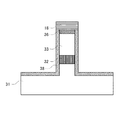
図1は、本発明の第1の実施形態に係る半導体光素子の上面模式図である。当該実施形態に係る半導体光素子は、2個のLDと、2個のQPSK変調器(変調領域13)と、偏波合波器14と、3個のPD20とが、同一基板上に備えられる半導体光集積素子である。ここで、2個のLDは、TE偏波(第1の偏波)を有する光を出力する第1LD11(第1の光源)と、TM偏波(第2の偏波)を有する光を出力する第2LD12(第2の光源)であり、ともに、波長調整が可能な分布帰還型(DFB)LDである。さらに、第1LD11及び第2LD12は、LD電極15を素子表面に備え、LD電極15の上面の一部を覆って形成される薄膜抵抗16を備えている。薄膜抵抗16の両端には、電極パッド21が設けられ、2個の電極パッド21の間に電圧を印加することにより、薄膜抵抗16に電流が流れ、薄膜抵抗16は発熱する。薄膜抵抗16は、流れる電流を制御することにより発熱量が制御される可変熱源であり、2個のLDは、薄膜抵抗16によって温度制御されることによって、波長調整が可能となる波長可変LDである。すなわち、薄膜抵抗16は、LDが出力する光の波長を温度によって調整するための抵抗体である。また、各LDの変調器側とは反対側に、光出力モニタであるPD20が配置されており、対応するLDと光学的に接続される。第1の偏波と第2の偏波は、TE偏波とTM偏波のように、異なる2つの偏波であり、素子の特性上、第1の偏波と第2の偏波は互いに直交しているのが望ましいが、これに限定されることはない。
本発明の第2の実施形態に係る半導体光素子は、第1の実施形態に係る半導体光素子と、2個の光源の波長に差異があるかを検出するための光部品をさらに備える点で異なっているが、それ以外は第1の実施形態に係る半導体光素子と同じ構造をしている。かかる光部品を備えることにより、第1の実施形態で説明した効果に加え、2個の光源の波長をより高い精度で制御することが出来るというさらなる効果を奏する。
本発明の第3の実施形態に係る半導体光素子は、第2の実施形態に係る半導体光素子と、リング共振器42と光導波路とを光学的に結合する箇所が、方向性結合器ではなく、MMI合分波器を用いている点で異なっているが、それ以外は第2の実施形態に係る半導体光素子と同じ構造をしている。
本発明の第4の実施形態に係る半導体光素子は、第3の実施形態に係る半導体光素子と、MMI合分波器の形状が異なっているが、それ以外は第3の実施形態に係る半導体光素子と同じ構造をしている。
本発明の第5の実施形態に係る半導体光素子は、第2乃至第4の実施形態に係る半導体光素子と、2個の光源の波長に差異があるかを検出するための光部品の構成が異なっているが、それ以外は第2乃至第4の実施形態に係る半導体光素子と同じ構造をしている。
本発明の第6の実施形態に係る半導体光素子は、光源として、分布ブラッグ反射型(DBR)の波長可変LDを用いていることを除いて、第1乃至第5の実施形態に係る半導体光素子と同じ構造をしている。光源にDBR−LDを用いることにより、第1乃至第5の実施形態と比較して、各光源の波長をより広い範囲で調整することが出来る。
本発明の第7の実施形態に係る半導体光素子は、光源として、LGLCを用いた波長可変LDを用いていることを除いて、第1乃至第5の実施形態に係る半導体光素子と同じ構造をしている。光源にLGLC−LDを用いることにより、第1乃至第6の実施形態と比較して、各光源の波長をさらにより広い範囲で調整することが出来る。
本発明の第8の実施形態に係る半導体光素子は、第1乃至第7の実施形態に係る半導体光素子を複数、同一半導体基板上に集積したアレイ半導体光素子である。
本発明の第9の実施形態に係る光モジュールは、第1乃至第8の実施形態に係る半導体光素子を備える光モジュールである。
光源を制御する信号であればよい。例えば、光源の薄膜提供への注入DC電流量(波長を制御する信号)にディザ信号を重畳してもよく、光源の波長制御方法に適した信号であればよい。
)が検出する信号を、第1ディザ信号及び第2ディザ信号の周波数それぞれで抽出することにより、第1の光源及び第2の光源それぞれが出力する光の強度を検出する。検出される第1LD11が出力する光の強度に基づいて、リング共振器を第1の光源の波長に対応して所定の特性となるよう制御する。たとえば、検出される第1LD11が出力する光の強度が最大となるように、リング共振器の透過波長を制御する。そして、検出される第2LD12が出力する光の強度に基づいて、リング共振器の所定の特性に応じて、光の強度を所定の範囲とすることにより、第2LD12が出力する光の波長を所定の範囲とすることが出来る。このようにして、一方の光源が出力する光の波長を他方の光源が出力する光の波長に近づけるよう制御することが出来る。理想的には、2個の光源が出力する光の波長が一致しているのが望ましい。なお、この場合、第2ディザ信号は、光強度を制御する信号(電圧信号)に重畳されるが、必ずしも電圧である必要はなく、光源を制御する信号であればよい。例えば、光源の薄膜提供への注入DC電流量(波長を制御する信号)にディザ信号を重畳してもよく、光源の波長制御方法に適した信号であればよい。
本発明の第10の実施形態に係る光モジュールの構成は、第9の実施形態に係る光モジュールと同じであるが、波長制御の方法が第9の実施形態と異なっている。
本発明の第11の実施形態に係る光モジュールの構成は、第9及び第10の実施形態に係る光モジュールと同じであるが、波長制御の方法が第9及び第10の実施形態と異なっている。
Claims (12)
- 第1の偏波を有する光を出力する第1の光源と、
前記第1の偏波と異なる偏波である第2の偏波を有する光を出力する第2の光源と、
前記第1の光源の出力側に光学的に接続され、前記第1の光源が出力する光を変調して光信号を出力する、第1の光変調器と、
前記第2の光源の出力側に光学的に接続され、前記第2の光源が出力する光を変調して光信号を出力する、第2の光変調器と、
前記第1の光変調器が出力する光信号と、前記第2の光変調器が出力する光信号と、を結合して結合光信号を出力する、光合波器と、
前記第1の光源及び前記第2の光源それぞれと光学的に接続するとともに、前記第1の光源及び前記第2の光源それぞれが出力する光の波長に差異があるかを検出するための、
リング共振器と、
前記リング共振器と光学的に接続するとともに、前記第1の光源及び前記第2の光源それぞれが出力する光を該素子が変換する光を検出する受光器と、
前記第1の光源に光学的に接続される第1の光導波路と、
前記第2の光源に光学的に接続される第2の光導波路と、
前記第1の光導波路と前記リング共振器を光学的に結合する、第1のマルチモード干渉型合分波器と、
前記第2の光導波路と前記リング共振器を光学的に結合する、第2のマルチモード干渉型合分波器と、
が、半導体基板上にともに集積される、半導体光素子。 - 請求項1に記載の半導体光素子であって、
前記第1の光源及び前記第2の光源の少なくとも一方は、波長可変レーザであり、
前記第1の光源及び前記第2の光源は、前記第1の光源又は第2の光源のいずれか一方の光源が出力する光の波長を、他方の光源が出力する光の波長に近づけることが可能である、
ことを特徴とする、半導体光素子。 - 請求項2に記載の半導体光素子であって、
前記波長可変レーザは、出力する光の波長を温度によって調整するための抵抗体を備える分布帰還型レーザである、
ことを特徴とする、半導体光素子。 - 請求項2に記載の半導体光素子であって、
前記波長可変レーザは、分布ブラッグ反射型レーザ又は横グレーティングアシスト横方向性結合器型レーザである、
ことを特徴とする、半導体光素子。 - 請求項1乃至4のいずれかに記載の半導体光素子であって、
前記第1のマルチモード干渉型合分波器及び前記第2のマルチモード干渉型合分波器は、ともに、光軸方向に沿って実効屈折率が変化する、
ことを特徴とする、半導体光素子。 - 請求項1乃至5のいずれかに記載の半導体光素子を、備える光モジュール。
- 請求項1乃至5のいずれかに記載の半導体光素子と、
前記受光器が検出する信号に基づいて、前記第1の光源又は第2の光源のいずれかの一方の光源が出力する光の波長を、他方の光源が出力する光の波長に近づけるよう、前記第1の光源及び/又は前記第2の光源を制御する、制御部と、
を備える光モジュール。 - 請求項7に記載の光モジュールであって、
前記第2の光源は波長可変レーザであり、
前記制御部は、前記第1の光源の光出力を制御する信号に、第1ディザ信号を重畳し、前記受光器が検出する信号を前記第1ディザ信号の周波数で抽出して、前記波長依存性を有する素子を前記第1の光源の波長に対応して所定の特性となるように制御し、
前記制御部は、前記第2の光源を制御する信号に、前記第1ディザ信号と異なる周波数を有する第2ディザ信号を重畳し、前記受光器が検出する信号を前記第2ディザ信号の周波数で抽出して、前記第2の光源の波長を前記波長依存性を有する素子の前記所定の特性に対応して所定の範囲となるように制御する、
ことを特徴とする、光モジュール。 - 請求項7に記載の光モジュールであって、
前記第1の光源及び前記第2の光源はともに波長可変レーザであり、
前記制御部は、前記第1の光源を制御する信号に、第1ディザ信号を重畳し、前記第2の光源を制御する信号に、前記第1ディザ信号と異なる周波数を有する第2ディザ信号を重畳し、前記受光器が検出する信号を、前記第1ディザ信号の周波数及び前記第2ディザ信号の周波数それぞれで抽出して、前記第1の光源の波長及び前記第2の光源の波長を前記波長依存性を有する素子の所定の特性に対応して、それぞれ所定の範囲となるように制御する、
ことを特徴とする、光モジュール。 - 請求項7に記載の光モジュールであって、
前記第2の光源は波長可変レーザであり、
前記半導体光素子は、
前記第1の光源の前記第1の光変調器側とは反対側において、前記第1の光源に光学的に接続されるとともに、前記第1の光源が出力する光の強度を検出する第1光強度受光器と、
前記第2の光源の前記第2の光変調器とは反対側において、前記第2の光源に光学的に接続されるとともに、前記第2の光源が出力する光の強度を検出する第2光強度受光器と、
をさらに備え、
前記制御部は、
前記第1の光源に対応するタイムスロットにおいて、前記第1光強度受光器及び前記第2光強度受光器それぞれに、前記第1の光源の波長検出するための所定のバイアス電圧を印加し、前記受光器が検出する信号に基づいて、前記波長依存性を有する素子を前記第1の光源の波長に対応して所定の特性となるように制御し、
前記第2の光源に対応するタイムスロットにおいて、前記第1光強度受光器及び前記第2光強度受光器それぞれに、前記第2の光源の波長検出するための所定のバイアス電圧を印加し、前記受光器が検出する信号に基づいて、前記第2の光源の波長を前記波長依存性を有する素子の前記所定の特性に対応して所定の範囲となるように制御する、
ことを特徴とする、光モジュール。 - 請求項7に記載の光モジュールであって、
前記第1の光源及び前記第2の光源はともに波長可変レーザであり、
前記半導体光素子は、
前記第1の光源の前記第1の光変調器側とは反対側において、前記第1の光源に光学的に接続されるとともに、前記第1の光源が出力する光の強度を検出する第1光強度受光器と、
前記第2の光源の前記第2の光変調器とは反対側において、前記第2の光源に光学的に接続されるとともに、前記第2の光源が出力する光の強度を検出する第2光強度受光器と、
をさらに備え、
前記制御部は、
前記第1の光源に対応するタイムスロットにおいて、前記第1光強度受光器及び前記第2光強度受光器それぞれに、前記第1の光源の波長検出するための所定のバイアス電圧を印加し、前記受光器が検出する信号に基づいて、前記第1の光源が出力する光の波長を前記波長依存を有する素子の特性に対応して所定の範囲内となるよう制御し、
前記第2の光源に対応するタイムスロットにおいて、前記第1光強度受光器及び前記第2光強度受光器それぞれに、前記第2の光源の波長検出するための所定のバイアス電圧を印加し、前記受光器が検出する信号に基づいて、前記第2の光源が出力する光の波長を前記波長依存を有する素子の特性に対応して所定の範囲内となるよう制御する、
ことを特徴とする、光モジュール。 - 請求項7に記載の光モジュールであって、
前記第1の光源及び前記第2の光源はともに波長可変レーザであり、
前記制御部は、前記受光器が検出する信号より、前記第1の光源が出力する光と前記第2の光源が出力する光とが前記波長依存性を有する素子において干渉して発生するビート信号を抽出して、前記第1の光源の波長及び前記第2の光源の波長を前記波長依存性を有する素子の所定の特性に対応して、それぞれ所定の範囲となるように制御する、
ことを特徴とする、光モジュール。
Priority Applications (2)
| Application Number | Priority Date | Filing Date | Title |
|---|---|---|---|
| JP2012029784A JP5877727B2 (ja) | 2012-02-14 | 2012-02-14 | 半導体光変調素子及び光モジュール |
| US13/765,220 US9164349B2 (en) | 2012-02-14 | 2013-02-12 | Optical semiconductor modulator device and optical module |
Applications Claiming Priority (1)
| Application Number | Priority Date | Filing Date | Title |
|---|---|---|---|
| JP2012029784A JP5877727B2 (ja) | 2012-02-14 | 2012-02-14 | 半導体光変調素子及び光モジュール |
Publications (3)
| Publication Number | Publication Date |
|---|---|
| JP2013168440A JP2013168440A (ja) | 2013-08-29 |
| JP2013168440A5 JP2013168440A5 (ja) | 2015-01-22 |
| JP5877727B2 true JP5877727B2 (ja) | 2016-03-08 |
Family
ID=48945592
Family Applications (1)
| Application Number | Title | Priority Date | Filing Date |
|---|---|---|---|
| JP2012029784A Active JP5877727B2 (ja) | 2012-02-14 | 2012-02-14 | 半導体光変調素子及び光モジュール |
Country Status (2)
| Country | Link |
|---|---|
| US (1) | US9164349B2 (ja) |
| JP (1) | JP5877727B2 (ja) |
Families Citing this family (21)
| Publication number | Priority date | Publication date | Assignee | Title |
|---|---|---|---|---|
| JP5652284B2 (ja) * | 2011-03-22 | 2015-01-14 | 富士通株式会社 | 光半導体素子 |
| KR20140117988A (ko) * | 2013-03-27 | 2014-10-08 | 한국전자통신연구원 | 편광 제어 장치 및 편광 제어 방법 |
| US9036669B2 (en) * | 2013-09-12 | 2015-05-19 | Futurewei Technologies, Inc. | Obtaining narrow line-width, full C-band tunability mirror for monolithic or hybrid integrated lasers |
| JP6446955B2 (ja) * | 2013-10-09 | 2019-01-09 | 住友電気工業株式会社 | 光送信モジュール |
| JP2015159191A (ja) * | 2014-02-24 | 2015-09-03 | 住友電気工業株式会社 | 光伝送装置 |
| US20160127070A1 (en) * | 2014-10-31 | 2016-05-05 | Inphi Corporation | Integrated two-channel spectral combiner and wavelength locker in silicon photonics |
| WO2017135381A1 (ja) * | 2016-02-04 | 2017-08-10 | 日本電信電話株式会社 | 光送信器及び光強度モニタ方法 |
| CN106788765B (zh) * | 2016-11-30 | 2019-05-14 | 中国科学院半导体研究所 | 硅基高速双载波双偏振调制器集成芯片 |
| US9835928B1 (en) * | 2017-02-13 | 2017-12-05 | Futurewei Technologies, Inc. | Optical N-level quadrature amplitude modulation (NQAM) tuned by dithering associated heaters |
| JP2018133466A (ja) * | 2017-02-16 | 2018-08-23 | 沖電気工業株式会社 | 半導体光学素子 |
| US10509295B2 (en) * | 2017-03-15 | 2019-12-17 | Elenion Technologies, Llc | Bias control of optical modulators |
| US10509243B2 (en) * | 2017-03-15 | 2019-12-17 | Elenion Technologies, Llc | Bias control of optical modulators |
| CN108933630B (zh) * | 2018-06-13 | 2019-11-12 | 华中科技大学 | 一种调制格式与偏振复用切换的光发射系统 |
| WO2019239683A1 (ja) * | 2018-06-14 | 2019-12-19 | 三菱電機株式会社 | 光変調器及び光送信モジュール |
| GB2575653A (en) * | 2018-07-17 | 2020-01-22 | Univ College Cork National Univ Of Ireland | Phase modulator for optical signal using multimode interference couplers |
| JP7091969B2 (ja) * | 2018-09-25 | 2022-06-28 | 日本電信電話株式会社 | 光変調器モジュール |
| WO2020136053A1 (en) * | 2018-12-28 | 2020-07-02 | Rockley Photonics Limited | Wdm receiver and method of operation thereof |
| WO2020162451A1 (ja) * | 2019-02-06 | 2020-08-13 | 古河電気工業株式会社 | 光機能素子およびレーザ素子 |
| CN110779440B (zh) * | 2019-10-12 | 2021-05-07 | 浙江大学 | 一种基于马赫泽德干涉仪结构的偏振不敏感光开关 |
| WO2021149647A1 (ja) * | 2020-01-22 | 2021-07-29 | 古河電気工業株式会社 | 半導体素子 |
| CN115037374B (zh) * | 2022-04-28 | 2023-07-07 | 苏州大学 | 一种宽带双路偏振混沌激光产生方法及装置 |
Family Cites Families (28)
| Publication number | Priority date | Publication date | Assignee | Title |
|---|---|---|---|---|
| US4368645A (en) * | 1980-09-26 | 1983-01-18 | United Technologies Corporation | Optical pressure sensor |
| JP2003060578A (ja) | 2001-08-13 | 2003-02-28 | Matsushita Electric Ind Co Ltd | 光送信機、光受信機及び光波長多重システム |
| JP2005172975A (ja) * | 2003-12-09 | 2005-06-30 | Nippon Telegr & Teleph Corp <Ntt> | 波長可変光フィルタ制御方法および波長可変光フィルタ装置 |
| JP4422661B2 (ja) * | 2005-08-31 | 2010-02-24 | 富士通株式会社 | 差動4位相偏移変調器の駆動電圧設定方法 |
| JP4719115B2 (ja) * | 2006-09-21 | 2011-07-06 | 富士通株式会社 | 光集積素子及び波長変換方式 |
| JP5088052B2 (ja) * | 2007-08-31 | 2012-12-05 | 富士通株式会社 | 偏光多重送信装置 |
| JP4701232B2 (ja) * | 2007-12-28 | 2011-06-15 | 住友大阪セメント株式会社 | 光変調器 |
| US8238759B2 (en) * | 2008-02-14 | 2012-08-07 | Infinera Corporation | High capacity transmitter implemented on a photonic integrated circuit |
| US20100067918A1 (en) * | 2008-04-18 | 2010-03-18 | New Jersey Institute Of Technology | Ultra-miniaturized thz communication device and system |
| JP5186993B2 (ja) | 2008-04-30 | 2013-04-24 | 富士通株式会社 | 偏波多重光送受信装置 |
| US8098989B2 (en) * | 2008-05-08 | 2012-01-17 | Nec Laboratories America, Inc. | All-optical wavelength conversion for a polarization multiplexing optical signal |
| JP2010050135A (ja) * | 2008-08-19 | 2010-03-04 | Nec Corp | 半導体光集積素子および光通信装置 |
| JP5083134B2 (ja) * | 2008-09-10 | 2012-11-28 | 富士通株式会社 | 偏波多重光送信器およびその制御方法 |
| JP5476697B2 (ja) * | 2008-09-26 | 2014-04-23 | 富士通株式会社 | 光信号送信装置 |
| US20100150555A1 (en) * | 2008-12-12 | 2010-06-17 | Zinan Wang | Automatic polarization demultiplexing for polarization division multiplexed signals |
| US8611751B2 (en) * | 2009-02-26 | 2013-12-17 | Alcatel Lucent | System, apparatus and method for communicating data via polarization multiplexing |
| US8401405B2 (en) * | 2009-05-28 | 2013-03-19 | Freedom Photonics, Llc. | Monolithic widely-tunable coherent receiver |
| JP2011003591A (ja) | 2009-06-16 | 2011-01-06 | Sumitomo Electric Ind Ltd | 波長ロッカー集積型半導体レーザ素子 |
| JP5446586B2 (ja) * | 2009-08-21 | 2014-03-19 | 富士通株式会社 | 偏波多重光送信器および偏波多重光信号の制御方法 |
| WO2011027895A1 (ja) * | 2009-09-07 | 2011-03-10 | 古河電気工業株式会社 | Plc型復調器及び光伝送システム |
| FR2950746B1 (fr) * | 2009-09-30 | 2013-09-06 | Alcatel Lucent | Modulateur avec marquage de polarisation |
| JP5457873B2 (ja) * | 2010-02-18 | 2014-04-02 | 住友電工デバイス・イノベーション株式会社 | 波長可変レーザの制御方法 |
| JP2011176070A (ja) * | 2010-02-24 | 2011-09-08 | Opnext Japan Inc | 波長可変レーザ装置 |
| JP2011188213A (ja) * | 2010-03-08 | 2011-09-22 | Fujitsu Ltd | 光信号送信装置、光増幅装置、光減衰装置及び光信号送信方法 |
| WO2011114753A1 (ja) * | 2010-03-19 | 2011-09-22 | 日本電信電話株式会社 | 光変調器 |
| JP5683237B2 (ja) * | 2010-11-29 | 2015-03-11 | 株式会社日立製作所 | 偏波多重光伝送システム、偏波多重光送信器及び偏波多重光受信器 |
| US8582933B2 (en) * | 2011-01-07 | 2013-11-12 | Alcatel Lucent | Scalable waveguide-mode coupler for an optical receiver or transmitter |
| US9170438B2 (en) * | 2012-07-10 | 2015-10-27 | Infinera Corporation | Suppression of resonant polarization conversion in photonic integrated circuits |
-
2012
- 2012-02-14 JP JP2012029784A patent/JP5877727B2/ja active Active
-
2013
- 2013-02-12 US US13/765,220 patent/US9164349B2/en active Active
Also Published As
| Publication number | Publication date |
|---|---|
| JP2013168440A (ja) | 2013-08-29 |
| US20130209021A1 (en) | 2013-08-15 |
| US9164349B2 (en) | 2015-10-20 |
Similar Documents
| Publication | Publication Date | Title |
|---|---|---|
| JP5877727B2 (ja) | 半導体光変調素子及び光モジュール | |
| US9887780B2 (en) | Chip-based advanced modulation format transmitter | |
| US9755753B2 (en) | Tunable U-laser transmitter with integrated Mach-Zehnder Modulator | |
| US8559470B2 (en) | Method and system for hybrid integration of a tunable laser and a phase modulator | |
| JP6876383B2 (ja) | 波長可変光源 | |
| US8867578B2 (en) | Method and system for hybrid integration of a tunable laser for a cable TV transmitter | |
| US7738794B2 (en) | Optical transmitter | |
| US8605766B2 (en) | Method and system for hybrid integration of a tunable laser and a mach zehnder modulator | |
| JP5268733B2 (ja) | 光導波素子とその製造方法、半導体素子、レーザモジュール及び光伝送システム | |
| US20170163000A1 (en) | Photonic Integrated Circuit Including Compact Lasers With Extended Tunability | |
| JP5212475B2 (ja) | 波長可変光送信機 | |
| WO2013114578A1 (ja) | 光送信器および光送信器の制御方法 | |
| JP2017098362A (ja) | 光集積素子及び光通信装置 | |
| JP2017216384A (ja) | 波長可変レーザ | |
| JP2010027664A (ja) | 光半導体装置 | |
| US20170163001A1 (en) | Photonic Integrated Circuit Including Compact Lasers With Extended Tunability | |
| US8666200B2 (en) | Optical modulation device, driving method of optical modulation device, and manufacturing method of optical modulation device | |
| US20170207603A1 (en) | Laser arrays comprising compact lasers with extended tunability | |
| WO2015162671A1 (ja) | 波長可変レーザ光源、光送信器及び光送受信器モジュール | |
| US20170201070A1 (en) | Compact lasers with extended tunability | |
| JP2013156352A (ja) | 光変調器及び光送信モジュール | |
| JP2010034114A (ja) | レーザ装置、レーザモジュールおよび波長多重光通信システム | |
| JP5505230B2 (ja) | 光半導体素子 | |
| Aihara et al. | Heterogeneously integrated membrane DFB laser and Si Mach-Zehnder modulator on Si photonics platform |
Legal Events
| Date | Code | Title | Description |
|---|---|---|---|
| A521 | Request for written amendment filed |
Free format text: JAPANESE INTERMEDIATE CODE: A523 Effective date: 20141128 |
|
| A621 | Written request for application examination |
Free format text: JAPANESE INTERMEDIATE CODE: A621 Effective date: 20141128 |
|
| A977 | Report on retrieval |
Free format text: JAPANESE INTERMEDIATE CODE: A971007 Effective date: 20150819 |
|
| A131 | Notification of reasons for refusal |
Free format text: JAPANESE INTERMEDIATE CODE: A131 Effective date: 20150825 |
|
| A521 | Request for written amendment filed |
Free format text: JAPANESE INTERMEDIATE CODE: A523 Effective date: 20151022 |
|
| TRDD | Decision of grant or rejection written | ||
| A01 | Written decision to grant a patent or to grant a registration (utility model) |
Free format text: JAPANESE INTERMEDIATE CODE: A01 Effective date: 20160105 |
|
| A61 | First payment of annual fees (during grant procedure) |
Free format text: JAPANESE INTERMEDIATE CODE: A61 Effective date: 20160126 |
|
| R150 | Certificate of patent or registration of utility model |
Ref document number: 5877727 Country of ref document: JP Free format text: JAPANESE INTERMEDIATE CODE: R150 |
|
| R250 | Receipt of annual fees |
Free format text: JAPANESE INTERMEDIATE CODE: R250 |
|
| S533 | Written request for registration of change of name |
Free format text: JAPANESE INTERMEDIATE CODE: R313533 |
|
| R350 | Written notification of registration of transfer |
Free format text: JAPANESE INTERMEDIATE CODE: R350 |
|
| R250 | Receipt of annual fees |
Free format text: JAPANESE INTERMEDIATE CODE: R250 |
|
| R250 | Receipt of annual fees |
Free format text: JAPANESE INTERMEDIATE CODE: R250 |
|
| R250 | Receipt of annual fees |
Free format text: JAPANESE INTERMEDIATE CODE: R250 |
|
| R250 | Receipt of annual fees |
Free format text: JAPANESE INTERMEDIATE CODE: R250 |
|
| R250 | Receipt of annual fees |
Free format text: JAPANESE INTERMEDIATE CODE: R250 |