WO2025028283A1 - パワー半導体測定装置およびプローブ治具 - Google Patents
パワー半導体測定装置およびプローブ治具 Download PDFInfo
- Publication number
- WO2025028283A1 WO2025028283A1 PCT/JP2024/025774 JP2024025774W WO2025028283A1 WO 2025028283 A1 WO2025028283 A1 WO 2025028283A1 JP 2024025774 W JP2024025774 W JP 2024025774W WO 2025028283 A1 WO2025028283 A1 WO 2025028283A1
- Authority
- WO
- WIPO (PCT)
- Prior art keywords
- power semiconductor
- contact
- probe jig
- plate body
- inspection circuit
- Prior art date
- Legal status (The legal status is an assumption and is not a legal conclusion. Google has not performed a legal analysis and makes no representation as to the accuracy of the status listed.)
- Pending
Links
Images











Classifications
-
- G—PHYSICS
- G01—MEASURING; TESTING
- G01R—MEASURING ELECTRIC VARIABLES; MEASURING MAGNETIC VARIABLES
- G01R1/00—Details of instruments or arrangements of the types included in groups G01R5/00 - G01R13/00 and G01R31/00
- G01R1/02—General constructional details
- G01R1/06—Measuring leads; Measuring probes
- G01R1/067—Measuring probes
-
- G—PHYSICS
- G01—MEASURING; TESTING
- G01R—MEASURING ELECTRIC VARIABLES; MEASURING MAGNETIC VARIABLES
- G01R31/00—Arrangements for testing electric properties; Arrangements for locating electric faults; Arrangements for electrical testing characterised by what is being tested not provided for elsewhere
- G01R31/26—Testing of individual semiconductor devices
-
- G—PHYSICS
- G01—MEASURING; TESTING
- G01R—MEASURING ELECTRIC VARIABLES; MEASURING MAGNETIC VARIABLES
- G01R31/00—Arrangements for testing electric properties; Arrangements for locating electric faults; Arrangements for electrical testing characterised by what is being tested not provided for elsewhere
- G01R31/28—Testing of electronic circuits, e.g. by signal tracer
Definitions
- This disclosure relates to a power semiconductor measuring device and a probe jig.
- Power semiconductor measuring equipment is used to measure (inspect) power semiconductor devices through which large currents flow. As power semiconductor devices become smaller, the pitch between the terminals of the power semiconductor devices becomes narrower.
- a contact probe made of stacked metal sheets has been proposed.
- a contact probe With a contact probe, each of the stacked metal sheets is brought into contact with a corresponding terminal on the power semiconductor device, and each of the metal sheets in contact with the terminal is electrically connected to an inspection circuit via lead wires, thereby measuring the power semiconductor device.
- Patent Document 1 a contact probe that does not use lead wires has been proposed.
- This contact probe employs a structure in which each of the thin metal plates that contact the terminals of the power semiconductor device is brought into contact with an inspection circuit.
- a power semiconductor measuring device When inspecting a power semiconductor device, a power semiconductor measuring device generally has a mechanism for biasing (loading) the power semiconductor device onto the stage in order to pass a large current through the power semiconductor device. To achieve automation, it is necessary to transport the power semiconductor device without interfering with this mechanism. For this reason, with the contact probe described above, there is a demand for the contact probe to quickly transition from a state in which it is in contact with the inspection circuit to a state in which it is not in contact when the power semiconductor device is unloaded.
- This disclosure has been made as part of such development, and one objective is to provide a power semiconductor measuring device that can automate a series of measurements of power semiconductor devices and shorten the time required for the measurements, and another objective is to provide a probe fixture for use in such a power semiconductor measuring device.
- the power semiconductor measuring device is a power semiconductor measuring device that measures the electrical characteristics of a power semiconductor device, and includes an inspection circuit section, a probe jig with stacked contact plates, and a release mechanism.
- the inspection circuit section measures the electrical characteristics of the power semiconductor device.
- the probe jig with stacked contact plates comes into contact with the power semiconductor device and also comes into contact with the inspection circuit section, thereby electrically connecting the power semiconductor device to the inspection circuit section.
- the release mechanism releases the probe jig from a state in which the power semiconductor device is electrically connected to the inspection circuit section to a state in which the probe jig is not in contact with the inspection circuit section.
- the probe jig is a probe jig including one or more contact plates that contact a power semiconductor device.
- the contact plate includes a plate body, a first arm portion, and a second arm portion.
- the plate body has a width in a first direction, extends in a second direction intersecting the first direction, and has a first end portion and a second end portion that face each other at a distance in the second direction.
- the first arm portion extends from the first end portion of the plate body toward the side opposite the side where the second end portion is located, away from the plate body.
- the second arm portion extends from the second end portion of the plate body.
- the power semiconductor measuring device is provided with a release mechanism that releases the probe jig from a state in which the power semiconductor device is electrically connected to the inspection circuit section to a state in which the probe jig is not in contact with the inspection circuit section.
- This allows the probe jig to quickly transition from a state in which it is in contact with the inspection circuit section to a state in which it is not in contact with the inspection circuit section.
- it is possible to automate a series of measurements of the power semiconductor device, contributing to shortening the time required for measurements.
- the probe fixture disclosed herein can be used in a power semiconductor measuring device to automate a series of measurements on a power semiconductor device, helping to reduce the time required for measurements.
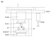
- FIG. 1 is a side view showing a power semiconductor measurement device according to a first embodiment
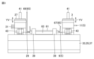
- FIG. 2 is a front view showing the power semiconductor measurement device in the embodiment
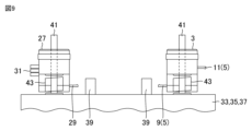
- FIG. 13 is a side view showing a first probe jig and a second probe jig installed on the stage main body in the embodiment.
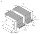
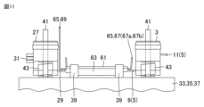
- FIG. 2 is a perspective view showing a first probe jig and a second probe jig installed on a stage main body in the embodiment.
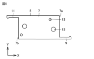
- FIG. 11 is a plan view showing a first contact plate applied to a first probe jig in the embodiment.
- FIG. 2 is a first perspective view for explaining a structure of a first probe jig in the embodiment.
- FIG. 13 is a second perspective view for explaining a structure of the first probe jig in the embodiment.
- FIG. 11 is a side view showing one step of measuring a power semiconductor device by the power semiconductor measuring device in the embodiment.
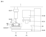
- FIG. 9 is a partially enlarged side view showing the inside of a dotted frame W1 shown in FIG. 8 in the embodiment. 9 is a side view showing a step performed after the step shown in FIG. 8 in the embodiment.
- FIG. 11 is a partially enlarged side view showing the inside of a dotted frame W2 shown in FIG. 10 in the embodiment.
- FIG. 11 is a side view showing a step performed after the step shown in FIG. 10 in the embodiment.
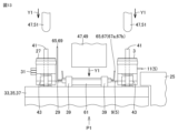
- FIG. 13 is a partially enlarged side view showing the state of the periphery of the stage main body in the step shown in FIG. 12 in the embodiment.
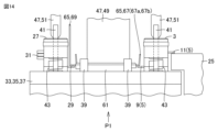
- FIG. 14 is a partially enlarged side view showing a step performed after the step shown in FIG. 13 in the embodiment.
- FIG. 15 is a partially enlarged side view showing a state of the first contact plate in the step shown in FIG. 14 in the embodiment.
- FIG. 15 is a partially enlarged side view showing a step performed after the step shown in FIG. 14 in the embodiment.
- FIG. 13 is a plan view showing a first contact plate of a first probe jig in a power semiconductor measurement apparatus according to a second embodiment.
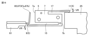
- FIG. 13 is a partially enlarged side view showing a state of a first contact plate during measurement of the power semiconductor device in the embodiment.
- FIG. FIG. 11 is a side view showing a power semiconductor measurement device according to a third embodiment.
- FIG. 13 is a side view showing a first probe jig and a second probe jig installed on the stage main body in the embodiment.
- FIG. 2 is a perspective view showing a first probe jig and a second probe jig installed on a stage main body in the embodiment.
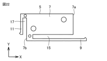
- FIG. 11 is a plan view showing a first contact plate applied to a first probe jig in the embodiment.
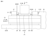
- 10 is a partially enlarged side view showing one step of measuring a power semiconductor device by the power semiconductor measuring device in the embodiment.
- FIG. 13 is a partially enlarged side view showing a state of a first contact plate during measurement of the power semiconductor device in the embodiment.
- FIG. 24 is a partially enlarged side view showing a step performed after the step shown in FIG. 23 in the embodiment.
- Embodiment 1 An example of a power semiconductor measuring device according to a first embodiment and a probe jig used therein will be described.
- the power semiconductor measuring device 1 includes a first probe jig 3 for large current terminals as probe jigs, a second probe jig 27 for signal terminals, an inspection circuit section 25, and a stage unit 33.
- the stage unit 33 has a stage body 35 including a cooling stage 37.
- the first probe jig 3 and the second probe jig 27 are installed on the stage body 35.
- the stage unit 33 also has a stage drive section 45 that drives the stage body 35 horizontally (front, back, left, right).
- the stage drive section 45 moves the stage body 35 between a measurement position P1 where the power semiconductor module 61 is measured, and a load/unload position P2 where the power semiconductor module 61 is loaded and unloaded.
- the inspection circuit section 25 is disposed near the stage body 35 when it is disposed at the measurement position P1.
- a positioning guide 39 that determines the position of the power semiconductor module 61 is disposed on the stage body 35.
- the power semiconductor measuring device 1 further includes a press unit 47 including a module pressing section 49 and a probe jig load plunger 51 serving as a probe pressing section.
- the power semiconductor module 61 placed on the stage body 35 is pressed toward the stage body 35 by the module pressing section 49 at the measurement position P1.
- the first probe jig 3 and the second probe jig 27 are pressed toward the stage body 35 by the probe jig load plunger 51 having a spring mechanism.
- the power semiconductor module 61 comes into contact with each of the first probe jig 3 and the second probe jig 27 by the press unit 47, thereby electrically connecting them.
- the lead terminals 67 related to the large current are electrically connected to the first probe jig 3, and the lead terminals 69 related to the signal current are electrically connected to the second probe jig 27.
- the first probe jig 3 is also electrically connected to the inspection circuit section 25.
- the lead terminals 67 related to the large current in the power semiconductor module 61 are electrically connected to the inspection circuit section 25 via the first probe jig 3.
- the power semiconductor measuring device 1 also includes a transport unit 53 including a holding section 55 and a holding section drive section 57.
- the holding section 55 includes, for example, a mechanism for suction or gripping.
- the power semiconductor module 61 to be measured is loaded into the stage unit 33 by the holding section 55.
- the power semiconductor module 61 is unloaded from the stage unit 33 by the holding section 55.
- the position of the holding section 55 is changed by the holding section drive section 57.
- the first probe jig 3 for large currents and the second probe jig 27 for signal terminals, which are arranged on the stage main body 35 (stage unit 33), will be described in more detail.
- the first probe jig 3 and the second probe jig 27 are arranged facing each other at a distance, sandwiching the area on which the power semiconductor module 61 is placed.
- the first contact plate 5 includes a plate body 7, a first arm portion 9 that comes into contact with the lead terminal 67 of the power semiconductor module 61, and a second arm portion 11 that comes into contact with the inspection circuit portion 25 (see FIG. 5).
- the first probe jig 3 is attached to the stage body 35 so as to be swingable in the vertical direction (arrow YV) with a coil spring 43 interposed between the first probe jig 3 and the stage body 35 and a support shaft 41 inserted through the coil spring 43 and the first probe jig 3 (holder 19).
- the support shaft 41 and the holder 19 through which the support shaft 41 is inserted function as guide members.
- the second probe jig 27 multiple second contact plates 29 for signal terminals are stacked.
- the second contact plates 29 contact the lead terminals 69 of the power semiconductor module 61.
- the second contact plates 29 have lead wire connection portions 31.
- the second probe jig 27 is also attached to the stage body 35 (stage unit 33) so as to be swingable in the vertical direction (arrow YV) with a coil spring 43 interposed between the second probe jig 27 and the stage unit 33 and a support shaft 41 inserted through the coil spring 43 and the second probe jig 27 (holder 19).
- each of the multiple first contact plates 5 has a plate body 7, a first arm portion 9, and a second arm portion 11.
- the plate body 7 is formed so as to have a width in the Y-axis direction as the first direction, and to extend in the X-axis direction as the second direction.
- the plate body 7 has a first end 7a and a second end 7b that face each other and are spaced apart in the X-axis direction.
- the first arm portion 9 is formed to extend from the first end 7a toward the side opposite the side where the second end 7b is located (the positive direction of the X-axis).
- the first arm portion 9 is formed to protrude from one end of the first end 7a in the width direction (the end on the negative Y-axis side).
- the second arm portion 11 is formed so as to extend from the second end portion 7b toward the opposite side (negative direction of the X-axis) from the side where the first end portion 7a is located.
- the second arm portion 11 is formed so as to protrude from the other end in the width direction (positive end of the Y-axis) of the second end portion 7b.
- the plate body 7 also has a plurality of through holes 13 formed therein. Each of the plurality of through holes 13 is formed to penetrate the plurality of first contact plates 5 when the first contact plates 5 are stacked.
- the first probe jig 3 which is made up of a plurality of stacked first contact plates 5. As shown in FIG. 6, the stacked first contact plates 5 are held by a holder 19.
- the holder 19 includes a first holder 19a, a second holder 19b, a third holder 19c, and a fourth holder 19d (see FIG. 6).
- the first probe jig 3 has a first part 3a electrically connected to the lead terminal 67a (positive electrode) of the power semiconductor module 61, and a second part 3b electrically connected to the lead terminal 67b (negative electrode).
- a plurality of stacked first contact plates 5 are sandwiched between the first holder 19a and the second holder 19b.
- the stacked first contact plates 5 are sandwiched between the second holder 19b and the third holder 19c.
- the stacked first contact plates 5 are stacked such that the first arm portions 9 are stacked on one another and the second arm portions 11 are stacked on one another.
- Each of the first holder 19a, the second holder 19b, and the third holder 19c has an opening formed therein that communicates with the through hole 13 formed in the first contact plate 5.
- the stacked first contact plate 5 is held between the first holder 19a and the second holder 19b by inserting a support rod 21 as a support member into the opening formed in the first holder 19a, the through hole 13 formed in the stacked first contact plate 5, and the opening formed in the second holder 19b.
- the stacked first contact plates 5 are held between the third holder 19c and the second holder 19b by inserting a support rod 21 as a support member into an opening formed in the third holder 19c, a through hole 13 formed in the stacked first contact plates 5, and an opening formed in the second holder 19b.
- the first holder 19a, the second holder 19b, the third holder 19c, and the support rod 21 are each formed from an insulating material.
- the first holder 19a, the second holder 19b, the third holder 19c, and the support rod 21 may each be formed from a conductive material. In this case, it is necessary to interpose an insulating material between the support rod 21 and the first contact plate 5. It is also necessary to interpose an insulating material between the first holder 19a, the second holder 19b, and the third holder 19c, and the first contact plate 5.
- each of the first part 3a and the second part 3b it is not necessarily necessary to electrically insulate the stacked first contact plates 5 from each other, but an insulating sheet or the like may be sandwiched between the first contact plates 5. In this case, interference between adjacent first contact plates 5 is suppressed, and deformation of the first arm portion 9 or the second arm portion 11 can be promoted.
- the stacked first contact plates 5 are further held by a fourth holder 19d.
- the fourth holder 19d is arranged to bridge the stacked first contact plates 5 between the first holder 19a and the third holder 19c.
- the fourth holder 19d has a shaft hole 23 formed in both the part on the first holder 19a side and the part on the third holder 19c side.
- a coil spring 43 is attached to the support shaft 41 that is erected on the stage body 35.
- the support shaft 41 is inserted into the shaft hole 23 formed in the fourth holder 19d in such a manner that the coil spring 43 is interposed between the stage body 35 and the fourth holder 19d.
- the support shaft 41 is inserted into the coil spring 43 and the shaft hole 23 in such a manner that the coil spring 43 is interposed between the stage body 35 and the first probe jig 3. Note that in FIG. 7, the coil spring 43 and the support shaft 41 located at the back are not shown in order to avoid cluttering the drawing.
- the first probe jig 3 is attached to the stage body 35 so as to be swingable up and down by the elastic force of the coil spring 43 and the pressing force of the press unit 47, with the shaft hole 23 and the support shaft 41 inserted into the shaft hole 23 as guide members.
- the second probe jig 27 for the signal terminal will be described.
- a plurality of second contact plates 29 are stacked.
- the stacked plurality of second contact plates 29 are held by a holder 19 or the like.
- the second contact plates 29 come into contact with the lead terminals 69 of the power semiconductor module 61.
- the second contact plates 29 have a lead wire connection portion 31.
- a connector (not shown) of a control lead wire that supplies a signal current is connected to the lead wire connection portion 31.
- the second probe jig 27 has a support shaft 41 inserted through the coil spring 43 and the holder 19, with the coil spring 43 interposed between the stage body 35 and the second probe jig 27.
- the second probe jig 27 is attached to the stage body 35 so that it can swing up and down due to the elastic force of the coil spring 43 and the pressing force of the press unit 47.
- first probe jig 3 and second probe jig 27 etc. are formed with respect to the stage body 35 as follows.
- the first probe jig 3 and second probe jig 27 are pressed by the probe jig load plunger 51 and the first probe jig 3 and second probe jig 27 are positioned at their lowest points, there is a state in which the module pressing portion 49 is not in contact with the power semiconductor module 61.
- the first probe jig 3 and second probe jig 27 etc. are formed so that a gap is formed between the power semiconductor module 61 and the stage body 35.
- the power semiconductor measuring device 1 according to the first embodiment is configured as described above.
- the stages main body 35 (stage unit 33) is moved to the loading/unloading position P2 by the stage driving section 45.
- the power semiconductor module 61 to be measured is held by the holding section 55 of the transport unit 53, and moved to directly above the stage unit 33 placed at the loading/unloading position P2.
- the holding portion 55 is lowered to place the held power semiconductor module 61 on the stage body 35 (stage unit 33).
- the positioning guide 39 places the power semiconductor module 61 at a determined position on the stage body 35.
- the large current lead terminal 67 of the power semiconductor module 61 contacts the first arm portion 9 of the first probe jig 3. Also, the signal lead terminal 69 of the power semiconductor module 61 contacts the second contact plate 29 of the second probe jig 27.
- the stage main body 35 (stage unit 33) on which the power semiconductor module 61 is placed is moved to the measurement position P1 by the stage driving unit 45.
- the module pressing unit 49 of the press unit 47 is lowered.
- the probe jig load plunger 51 also descends.
- the probe jig load plunger 51 is brought into contact with each of the first probe jig 3 and the second probe jig 27, and each of the first probe jig 3 and the second probe jig 27 is pressed downward against the elastic force of the coil spring 43, so that the first probe jig 3 and the second probe jig 27 are positioned at their lowest points.
- these actions cause the first arm portion 9 in contact with the lead terminal 67 to elastically deform toward the stage body 35 (see FIG. 14). Meanwhile, the second arm portion 11 in contact with the inspection circuit portion 25 elastically deforms upward. Also, the second contact plate 29 in contact with the lead terminal 69 elastically deforms toward the stage body 35 (not shown).
- a signal current is applied to the lead terminal 69 of the power semiconductor module 61 via the control lead wire (not shown), the lead wire connection portion 31, and the second probe jig 27.
- a large current is also applied to the lead terminal 67 of the power semiconductor module 61 via the inspection circuit portion 25, the second arm portion 11, and the first arm portion 9. The application of this signal current and large current allows the electrical characteristics of the power semiconductor module 61 to be measured (inspected).
- the module pressing portion 49 of the press unit 47 and the probe jig load plunger 51 are raised as indicated by the arrow Y2.
- the pressing force pressing the first probe jig 3 is eliminated, and the elastic force of the coil spring 43 causes the first probe jig 3 to rise as indicated by the arrow Y5.
- the second arm portion 11, which was in contact with the upper end of the inspection circuit portion 25, moves upward away from that upper end.
- the probe jig load plunger 51 and the coil spring 43 function as a release mechanism that releases the first probe jig 3 so that the second arm portion 11 (first probe jig 3) is not in contact with the inspection circuit portion 25.
- the stage drive unit 45 is driven to move the stage body 35 from the measurement position P1 to the load/unload position P2 (see FIG. 10).
- the stage body 35 on which the power semiconductor module 61 is placed can be moved without interfering with the probe jig load plunger 51 and the coil spring 43.
- the power semiconductor module 61 placed on the stage body 35 is adsorbed by the holder 55 of the transport unit 53 and removed from the stage body 35 (see FIG. 8). In this way, a series of measurements of the electrical characteristics of the power semiconductor module 61 is completed.
- the pressing force pressing the first probe jig 3 is eliminated.
- the first probe jig 3 is quickly raised by the elastic force of the coil spring 43.
- the second arm portion 11, which was in contact with the upper end of the inspection circuit unit 25, moves upward away from the upper end of the inspection circuit unit 25.
- Embodiment 2 An example of the power semiconductor measuring device 1 according to the second embodiment will be described. Here, an example of a variation of the first contact plate 5 applied to the first probe jig 3 will be described. Note that other configurations are similar to the configuration of the power semiconductor measuring device 1 described in the first embodiment, so the same members are given the same reference numerals, and the description will not be repeated unless necessary.
- the steps for measuring the power semiconductor module 61 using the above-mentioned power semiconductor measuring device 1 are the same as those described in the first embodiment.
- the power semiconductor module 61 is placed on the stage body 35, and the stage body 35 is moved to the measurement position P1, after which the electrical characteristics of the power semiconductor module 61 are measured.
- the power semiconductor module 61 is lowered by the module pressing portion 49, and the power semiconductor module 61 is brought into contact with the stage body 35 (see FIG. 14).
- the first contact plate 5 in the first probe jig 3 is provided with a first cutout portion 15 and a second cutout portion 17.
- the stroke amount VR when the first arm portion 9 and the second arm portion 11 are elastically deformed can be increased compared to the case where the first cutout portion 15 and the second cutout portion 17 are not formed.
- the first arm portion 9 can be made to follow the lead terminal 65 tilted relative to the first arm portion 9, and the first arm portion 9 can be brought into close contact with the lead terminal 65.
- the second arm portion 11 can be made to follow the uneven surface of the inspection circuit portion 25, and the second arm portion 11 can be brought into close contact with the surface of the inspection circuit portion 25.
- the electrical characteristics of the power semiconductor module 61 can be stably measured.
- Embodiment 3 An example of a power semiconductor measuring device according to the third embodiment and a probe jig used therein will be described.
- the first probe jig 3 and the second probe jig 27 are fixed to the stage body 35.
- the stacked first contact plates 5 are held by a holder 19.
- the holder 19 includes a first holder 19a, a second holder 19b, and a third holder 19c.
- no coil spring is interposed between the first probe jig 3 and the stage body 35, and the first holder 19a, the second holder 19b, and the third holder 19c are fixed to the stage body 35.
- each of the multiple first contact plates 5 has a plate body 7, a first arm portion 9, and a second arm portion 11.
- the plate body 7 has a width in the Y-axis direction and is formed to extend in the X-axis direction.
- the second probe jig 27 As shown in FIG. 21, in the second probe jig 27, a plurality of stacked second contact plates 29 are held by a holder 19. In this second probe jig 27 as well, there is no coil spring between the second probe jig 27 and the stage body 35, and the holder 19 is fixed to the stage body 35.
- the press unit 47 does not have a plunger for loading the plunger jig. Note that the rest of the configuration is the same as the configuration of the power semiconductor measuring device 1 described in the first embodiment, so the same members are given the same reference numerals and the description will not be repeated unless necessary.
- the stage unit 33 When the stage unit 33 is positioned at the measurement position P1, the second arm portion 11 of the first probe jig 3 comes into contact with the side of the inspection circuit portion 25. Next, as shown by the arrow Y1, the module pressing portion 49 of the press unit 47 is lowered to press the power semiconductor module 61 and bring the power semiconductor module 61 into contact with the stage body 35.
- these actions cause the first arm portion 9 in contact with the lead terminal 67 to elastically deform toward the stage body 35. Also, the second arm portion 11 in contact with the side of the inspection circuit section 25 to elastically deform toward the plate body 7. Meanwhile, the second contact plate 29 in contact with the lead terminal 69 to elastically deform toward the stage body 35 (not shown). In this state, the electrical characteristics of the power semiconductor module 61 are measured.
- the module pressing section 49 and the stage driving section 45 function as a release mechanism that releases the first probe jig 3 (second arm portion 11) so that it is not in contact with the inspection circuit section 25.
- the power semiconductor module 61 placed on the stage body 35 is adsorbed by the holder 55 of the transport unit 53 and removed from the stage body 35 (see FIG. 8). In this way, a series of measurements of the electrical characteristics of the power semiconductor module 61 is completed.
- the module pressing unit 49 is raised from the state in which the power semiconductor module 61 is pressed by the module pressing unit 49.
- the stage main body 35 is moved from the measurement position P1 toward the loading/unloading position P2 (see FIG. 19) by the stage driving unit 45.
- the second arm portion 11, which was in contact with the side of the inspection circuit section 25, moves away from the side of the inspection circuit section 25 toward the side.
- This allows the first probe jig 3 to quickly transition from a state in which it is in contact with the inspection circuit section 25 to a state in which it is not in contact with the inspection circuit section 25.
- it is possible to automate the measurement of a series of electrical characteristics of the power semiconductor module 61, contributing to shortening the time required for measurement.
- the inspection circuit unit 25 may be moved to move the second arm portion 11, which has been in contact with the side of the inspection circuit unit 25, away from the inspection circuit unit 25.
- the first probe jig 3 having the first contact plate 5 including the first arm portion 9 and the second arm portion 11 is used for a large current terminal of a power semiconductor module 61.
- the first probe jig 3 is not limited to this, and may also be used for a signal terminal of a power semiconductor module 61.
- the power semiconductor measuring device and first contact probe jig described in each embodiment can be combined in various ways as needed.
- This disclosure can be effectively used in a probe jig with stacked contact plates and a power semiconductor measuring device equipped with the probe jig.
- 1 Power semiconductor measuring device 3 First probe jig, 3a First part, 3b Second part, 5 First contact plate, 7 Plate body, 7a First end, 7b Second end, 9 First arm part, 11 Second arm part, 13 Through hole, 15 First cutout part, 17 Second cutout part, 19 Holder, 19a First holder, 19b Second holder, 19c Third holder, 19d Fourth holder, 21 Support rod, 23 Shaft hole, 25 Inspection circuit part, 27 Second probe jig, 29 Second contact plate, 31 Reed Wire connection part, 33 stage unit, 35 stage body, 37 cooling stage, 39 positioning guide, 41 support shaft, 43 coil spring, 45 stage drive part, 47 press unit, 49 module pressing part, 51 probe jig load plunger, 53 transport unit, 55 holding part, 57 holding part drive part, 61 power semiconductor module, 63 molded resin, 65, 67, 67a, 67b, 69 lead terminal, P1 measurement position, P2 loading/unloading position, Y1, Y2, Y3, Y4, Y5, YV
Landscapes
- Physics & Mathematics (AREA)
- General Physics & Mathematics (AREA)
- Engineering & Computer Science (AREA)
- General Engineering & Computer Science (AREA)
- Testing Of Individual Semiconductor Devices (AREA)
- Measuring Leads Or Probes (AREA)
Priority Applications (1)
| Application Number | Priority Date | Filing Date | Title |
|---|---|---|---|
| JP2025537837A JPWO2025028283A1 (https=) | 2023-08-02 | 2024-07-18 |
Applications Claiming Priority (2)
| Application Number | Priority Date | Filing Date | Title |
|---|---|---|---|
| JP2023125997 | 2023-08-02 | ||
| JP2023-125997 | 2023-08-02 |
Publications (1)
| Publication Number | Publication Date |
|---|---|
| WO2025028283A1 true WO2025028283A1 (ja) | 2025-02-06 |
Family
ID=94395096
Family Applications (1)
| Application Number | Title | Priority Date | Filing Date |
|---|---|---|---|
| PCT/JP2024/025774 Pending WO2025028283A1 (ja) | 2023-08-02 | 2024-07-18 | パワー半導体測定装置およびプローブ治具 |
Country Status (2)
| Country | Link |
|---|---|
| JP (1) | JPWO2025028283A1 (https=) |
| WO (1) | WO2025028283A1 (https=) |
Citations (10)
| Publication number | Priority date | Publication date | Assignee | Title |
|---|---|---|---|---|
| JPH11133060A (ja) * | 1997-10-31 | 1999-05-21 | Tani Denki Kogyo Kk | テスト用端子 |
| JP2002365308A (ja) * | 2001-06-08 | 2002-12-18 | Japan Electronic Materials Corp | 垂直ブレード型プローブ、垂直ブレード型プローブユニット及びそれを用いた垂直ブレード型プローブカード |
| WO2004102207A1 (ja) * | 2003-05-13 | 2004-11-25 | Kabushiki Kaisha Nihon Micronics | 通電試験用プローブ |
| KR20060101914A (ko) * | 2005-03-22 | 2006-09-27 | 주식회사 씨어테크 | 웨이퍼 검사용 프로브카드 |
| JP2008151515A (ja) * | 2006-12-14 | 2008-07-03 | Micronics Japan Co Ltd | プローブおよびその製造方法 |
| JP2009063381A (ja) * | 2007-09-05 | 2009-03-26 | Japan Electronic Materials Corp | プローブ |
| JP2013171005A (ja) * | 2012-02-22 | 2013-09-02 | Micronics Japan Co Ltd | 非接触型プローブカード |
| JP2016148566A (ja) * | 2015-02-12 | 2016-08-18 | 日本電子材料株式会社 | プローブカード |
| JP2017142220A (ja) * | 2016-02-10 | 2017-08-17 | インクス株式会社 | パワー半導体用プローブ装置 |
| CN208520905U (zh) * | 2018-07-18 | 2019-02-19 | 罗日伟 | 一种fpc测试用的探针 |
-
2024
- 2024-07-18 JP JP2025537837A patent/JPWO2025028283A1/ja active Pending
- 2024-07-18 WO PCT/JP2024/025774 patent/WO2025028283A1/ja active Pending
Patent Citations (10)
| Publication number | Priority date | Publication date | Assignee | Title |
|---|---|---|---|---|
| JPH11133060A (ja) * | 1997-10-31 | 1999-05-21 | Tani Denki Kogyo Kk | テスト用端子 |
| JP2002365308A (ja) * | 2001-06-08 | 2002-12-18 | Japan Electronic Materials Corp | 垂直ブレード型プローブ、垂直ブレード型プローブユニット及びそれを用いた垂直ブレード型プローブカード |
| WO2004102207A1 (ja) * | 2003-05-13 | 2004-11-25 | Kabushiki Kaisha Nihon Micronics | 通電試験用プローブ |
| KR20060101914A (ko) * | 2005-03-22 | 2006-09-27 | 주식회사 씨어테크 | 웨이퍼 검사용 프로브카드 |
| JP2008151515A (ja) * | 2006-12-14 | 2008-07-03 | Micronics Japan Co Ltd | プローブおよびその製造方法 |
| JP2009063381A (ja) * | 2007-09-05 | 2009-03-26 | Japan Electronic Materials Corp | プローブ |
| JP2013171005A (ja) * | 2012-02-22 | 2013-09-02 | Micronics Japan Co Ltd | 非接触型プローブカード |
| JP2016148566A (ja) * | 2015-02-12 | 2016-08-18 | 日本電子材料株式会社 | プローブカード |
| JP2017142220A (ja) * | 2016-02-10 | 2017-08-17 | インクス株式会社 | パワー半導体用プローブ装置 |
| CN208520905U (zh) * | 2018-07-18 | 2019-02-19 | 罗日伟 | 一种fpc测试用的探针 |
Also Published As
| Publication number | Publication date |
|---|---|
| JPWO2025028283A1 (https=) | 2025-02-06 |
Similar Documents
| Publication | Publication Date | Title |
|---|---|---|
| US8159245B2 (en) | Holding member for inspection, inspection device and inspecting method | |
| CN101604000B (zh) | 电子部件的测试装置用部件及该电子部件的测试方法 | |
| JP4045687B2 (ja) | Icデバイスのテスト用キャリアボード | |
| JP6721302B2 (ja) | 両面回路基板の検査装置 | |
| KR20160128668A (ko) | 엘이디검사용 프로브 및 이를 포함하는 콘텍장치 | |
| CN101231964A (zh) | 半导体元件稳压测试方法及稳压测试治具 | |
| JPH0943276A (ja) | プローブ装置に用いられるプローブカードデバイス | |
| US20230266361A1 (en) | Probe pin having improved gripping structure | |
| JP2010153672A (ja) | 半導体装置の製造装置およびその製造方法 | |
| WO2025028283A1 (ja) | パワー半導体測定装置およびプローブ治具 | |
| JP5643476B2 (ja) | 二重弾性機構プローブカード | |
| KR101322265B1 (ko) | 검사 탐침 장치 | |
| JP5423627B2 (ja) | 半導体装置の試験装置及び試験方法 | |
| JP2007285882A (ja) | 基板検査用接触子、基板検査用治具および基板検査装置 | |
| JP3225685B2 (ja) | コンタクトユニット及びic半導体装置の機能テスト方法 | |
| CN221746225U (zh) | 一种测试弹片及测试装置 | |
| KR100269953B1 (ko) | 반도체칩검사용소켓장치 | |
| JP3456146B2 (ja) | バンプ付電子部品のボンディング装置およびボンディング方法 | |
| JPH09153528A (ja) | プローブカードデバイス | |
| JP4817830B2 (ja) | プローバ、プローブ接触方法及びそのためのプログラム | |
| TW202136791A (zh) | 檢查治具、基板檢查裝置以及檢查裝置 | |
| JPH06201750A (ja) | 配線基板の検査装置 | |
| JP4334684B2 (ja) | 基板検査用センサおよび基板検査装置 | |
| KR20230120348A (ko) | 고전류 핀 소켓 및 그 제조방법 | |
| JP2024156428A (ja) | 検査治具および試験装置 |
Legal Events
| Date | Code | Title | Description |
|---|---|---|---|
| 121 | Ep: the epo has been informed by wipo that ep was designated in this application |
Ref document number: 24848938 Country of ref document: EP Kind code of ref document: A1 |
|
| ENP | Entry into the national phase |
Ref document number: 2025537837 Country of ref document: JP Kind code of ref document: A |
|
| WWE | Wipo information: entry into national phase |
Ref document number: 2025537837 Country of ref document: JP |
|
| NENP | Non-entry into the national phase |
Ref country code: DE |