WO2025023245A1 - 半導体装置 - Google Patents
半導体装置 Download PDFInfo
- Publication number
- WO2025023245A1 WO2025023245A1 PCT/JP2024/026322 JP2024026322W WO2025023245A1 WO 2025023245 A1 WO2025023245 A1 WO 2025023245A1 JP 2024026322 W JP2024026322 W JP 2024026322W WO 2025023245 A1 WO2025023245 A1 WO 2025023245A1
- Authority
- WO
- WIPO (PCT)
- Prior art keywords
- region
- layer
- base layer
- semiconductor substrate
- fwd
- Prior art date
- Legal status (The legal status is an assumption and is not a legal conclusion. Google has not performed a legal analysis and makes no representation as to the accuracy of the status listed.)
- Pending
Links
Images


Classifications
-
- H—ELECTRICITY
- H10—SEMICONDUCTOR DEVICES; ELECTRIC SOLID-STATE DEVICES NOT OTHERWISE PROVIDED FOR
- H10D—INORGANIC ELECTRIC SEMICONDUCTOR DEVICES
- H10D12/00—Bipolar devices controlled by the field effect, e.g. insulated-gate bipolar transistors [IGBT]
-
- H—ELECTRICITY
- H10—SEMICONDUCTOR DEVICES; ELECTRIC SOLID-STATE DEVICES NOT OTHERWISE PROVIDED FOR
- H10D—INORGANIC ELECTRIC SEMICONDUCTOR DEVICES
- H10D30/00—Field-effect transistors [FET]
- H10D30/60—Insulated-gate field-effect transistors [IGFET]
- H10D30/64—Double-diffused metal-oxide semiconductor [DMOS] FETs
- H10D30/66—Vertical DMOS [VDMOS] FETs
-
- H—ELECTRICITY
- H10—SEMICONDUCTOR DEVICES; ELECTRIC SOLID-STATE DEVICES NOT OTHERWISE PROVIDED FOR
- H10D—INORGANIC ELECTRIC SEMICONDUCTOR DEVICES
- H10D84/00—Integrated devices formed in or on semiconductor substrates that comprise only semiconducting layers, e.g. on Si wafers or on GaAs-on-Si wafers
- H10D84/80—Integrated devices formed in or on semiconductor substrates that comprise only semiconducting layers, e.g. on Si wafers or on GaAs-on-Si wafers characterised by the integration of at least one component covered by groups H10D12/00 or H10D30/00, e.g. integration of IGFETs
Definitions
- This disclosure relates to a semiconductor device in which an insulated gate bipolar transistor (hereinafter referred to as an IGBT) element having an insulated gate structure and a free wheel diode (hereinafter referred to as an FWD) element are formed on a common semiconductor substrate.
- IGBT insulated gate bipolar transistor
- FWD free wheel diode
- a semiconductor device in which an IGBT element is formed has been proposed (see, for example, Patent Document 1).
- a P-type base layer is disposed on an N-type drift layer, and an N-type emitter region is formed in a surface layer of the base layer.
- an N-type barrier region is disposed in the base layer to divide the base layer in the thickness direction so as to suppress the inflow of holes (i.e., carriers) from the drift layer to the base layer when the IGBT region is in an on-state.
- the base layer is composed of an ion-implanted layer in which P-type impurities are ion-implanted.
- the base layer is configured as follows, with the drift layer side of the base layer being the first base layer and the barrier region being the second base layer. That is, the first base layer is formed so that the first peak position where the P-type impurity concentration is maximum is located between the barrier region and the drift layer.
- the second base layer is formed so that the second peak position where the P-type impurity concentration is maximum is located between the emitter region and the barrier region.
- the first peak position is adjusted to be a position different from the boundary with the barrier region or the drift layer, for example, adjusted to be a position that is approximately the center between the barrier region and the drift layer.
- the second peak position is adjusted to be a position different from the boundary with the emitter region or the barrier region, for example, adjusted to be a position that is approximately the center between the emitter region and the barrier region.
- the inventors are considering a semiconductor device with a so-called RC (short for Reverse Conducting)-IGBT structure, in which an IGBT element and an FWD element are formed on a common semiconductor substrate.
- the inventors are considering making the base layer in the FWD element have the same structure as the IGBT element, in order to simplify the manufacturing process.
- the base layer, emitter region, etc. are formed on one side of the semiconductor substrate.
- the portion of the second base layer that constitutes one surface of the semiconductor substrate has an impurity concentration that is gradually reduced from the second peak position, and the impurity concentration is prone to variation. Therefore, in the FWD element, there is a possibility that the forward voltage will vary.
- the purpose of this disclosure is to provide a semiconductor device that can suppress variations in forward voltage.
- a semiconductor device has an IGBT region and an FWD region, and includes a drift layer of a first conductivity type, a base layer of a second conductivity type formed on the drift layer, a collector layer of the second conductivity type formed on the side of the drift layer opposite the base layer side in the IGBT region, and a cathode layer of the first conductivity type formed on the side of the drift layer opposite the base layer side in the FWD region, and includes a semiconductor substrate having a surface on the base layer side as one side and a surface on the collector layer and cathode layer side as the other side, a barrier region of the first conductivity type formed in the base layer and dividing the base layer into a first base layer on the drift layer side and a second base layer on the one side of the semiconductor substrate, a gate insulating film formed on the wall surface of a trench that penetrates the base layer and barrier region of the IGBT region to reach the drift layer, and a gate electrode formed on the gate insulating film;
- one surface of the semiconductor substrate connected to the first electrode includes a stabilization layer of the first conductivity type, and the first electrode is electrically connected to the contact region and the stabilization layer. Therefore, compared to when the one surface of the semiconductor substrate in the FWD region is composed of only the contact region and the second base layer, the proportion of the second base layer, which is prone to variations in impurity concentration, on the one surface of the semiconductor substrate can be reduced, and variations in the forward voltage of the FWD element can be suppressed.
- FIG. 1 is a cross-sectional view of a semiconductor device according to a first embodiment.
- FIG. 2 is a plan view of the semiconductor device shown in FIG.
- FIG. 2 is a perspective cross-sectional view of an FWD element.
- FIG. 1 is a diagram showing the relationship between the depth of a semiconductor substrate and the impurity concentration of a P-type impurity.
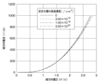
- FIG. 1 is a diagram showing the relationship between the forward voltage and forward current in an FWD element and the surface concentration of a stabilization layer.
- FIG. 13 is a plan view of a semiconductor device according to a second embodiment.
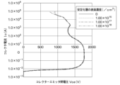
- FIG. 13 is a diagram showing the relationship between the collector-emitter voltage and collector current in an IGBT element, and the surface concentration of a stabilization layer.
- FIG. 1 is a diagram showing the relationship between the gate-emitter voltage and collector current in an IGBT element and the peak position of the stabilization layer.
- a semiconductor device according to a first embodiment will be described with reference to Figures 1 to 4.
- the semiconductor device according to the present embodiment is suitable for use as a power switching element used in a power supply circuit such as an inverter or a DC/DC converter.
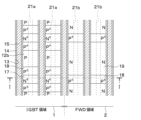
- the semiconductor device is configured with an IGBT region 1 that functions as an IGBT element, and an FWD region 2 that is adjacent to the IGBT region 1 and functions as an FWD element.
- the semiconductor device of this embodiment is an RC-IGBT in which the IGBT region 1 and FWD region 2 are formed in a common semiconductor substrate 10, which will be described later.
- the portion on the collector layer 24 located on the other surface 10b of the semiconductor substrate 10 is the IGBT region 1
- the portion on the cathode layer 25 located on the other surface 10b of the semiconductor substrate 10 is the FWD region 2.
- the semiconductor device has a semiconductor substrate 10 that constitutes an N - type drift layer 11.
- a P-type base layer 12 is formed on the drift layer 11.
- the surface of the semiconductor substrate 10 on the base layer 12 side will be referred to as one surface 10a, and the surface of the semiconductor substrate 10 opposite to the one surface 10a will be referred to as the other surface 10b.
- the semiconductor substrate 10 is composed of, for example, a silicon substrate.
- a plurality of trenches 13 are formed so as to penetrate the base layer 12 from the one surface 10a side to reach the drift layer 11.
- the base layer 12 is separated into a plurality of pieces by the trenches 13.
- the plurality of trenches 13 are formed in the IGBT region 1 and the FWD region 2, respectively.
- the plurality of trenches 13 are formed in a stripe shape with the longitudinal direction being a direction intersecting the arrangement direction of the IGBT region 1 and the FWD region 2 (i.e., the depth direction of the paper in FIG. 1).
- the longitudinal direction of the trenches 13 is also simply referred to as the longitudinal direction, and in FIG. 2, the vertical direction of the paper is the longitudinal direction.
- the distance between adjacent trenches 13 i.e., the pitch distance
- the pitch distance is, for example, about 2 ⁇ m.
- Each trench 13 is filled with a gate insulating film 14 formed to cover the wall surface of each trench 13, and a gate electrode 15 made of polysilicon or the like formed on this gate insulating film 14. This forms a trench gate structure.
- the gate electrode 15 arranged in the trench 13 formed in the IGBT region 1 is connected to a drive circuit (not shown) via a gate wiring (not shown). A predetermined pulse-shaped gate voltage is applied to this gate electrode 15.
- the gate electrode 15 arranged in the trench 13 formed in the FWD region 2 is electrically connected to the upper electrode 22 (described later) and is maintained at a predetermined potential.
- An N-type barrier region 16 having a higher impurity concentration than the drift layer 11 is formed in the base layer 12 so as to divide the base layer 12 in the depth direction of the semiconductor substrate 10.
- the portion of the base layer 12 on the drift layer 11 side is also referred to as the first base layer 12a
- the portion of the base layer 12 on the one surface 10a side of the semiconductor substrate 10 is also referred to as the second base layer 12b.
- the base layer 12 in the IGBT region 1 and the base layer 12 in the FWD region 2 have the same configuration.
- an N + type emitter region 17 having a higher impurity concentration than the drift layer 11 and a P + type contact region 18 having a higher impurity concentration than the base layer 12 are formed.
- the emitter region 17 and the contact region 18 are formed so that a part of the surface layer of the second base layer 12b remains. That is, the emitter region 17 and the contact region 18 are formed so that one surface 10a of the semiconductor substrate 10 includes the second base layer 12b, the emitter region 17, and the contact region 18 in the IGBT region 1.
- the emitter region 17 and the contact region 18 are formed so that the contact region 18, the emitter region 17, the contact region 18, and the second base layer 12b are repeatedly arranged in this order in the IGBT region 1 between adjacent trenches 13.
- a P + type contact region 18 having a higher impurity concentration than the base layer 12 is formed in the FWD region 2.
- the contact region 18 in the FWD region 2 has the same configuration as the contact region 18 in the IGBT region 1.
- an N-type stabilization layer 19 is formed in the FWD region 2.
- the one surface 10a of the semiconductor substrate 10 in the FWD region 2 is composed of the contact region 18 and the stabilization layer 19. That is, in the FWD region 2 of this embodiment, the stabilization layer 19 is formed in the entire region of the one surface 10a of the semiconductor substrate 10, except for the region where the contact region 18 is formed.
- the length of the contact region 18 along the longitudinal direction in the FWD region 2 is shorter than the length of the contact region 18 along the longitudinal direction in the IGBT region 1.
- the length of the contact region 18 along the longitudinal direction in the FWD region 2 and the length of the contact region 18 along the longitudinal direction in the IGBT region 1 can be changed as appropriate.
- the first base layer 12a and the second base layer 12b are ion-implanted layers formed by ion-implanting P-type impurities into the semiconductor substrate 10 and diffusing the P-type impurities.
- the second base layer 12b is formed so that a second peak position P2, where the impurity concentration is maximum, is located between the emitter region 17 and the barrier region 16.
- the first base layer 12a is formed so that a first peak position P1, where the impurity concentration is maximum, is located between the barrier region 16 and the drift layer 11.
- FIG. 4 shows the relationship between the P-type impurity concentration along the line IV-IV in FIG. 1 and the depth from the surface 10a of the semiconductor substrate 10.
- the first peak position P1 is adjusted to be at a position different from the boundary between the first base layer 12a and the barrier region 16 or the drift layer 11, for example, adjusted to a position that is approximately the center between the barrier region 16 and the drift layer 11.
- the second peak position P2 is adjusted to be at a position different from the boundary between the second base layer 12b and the emitter region 17 or the barrier region 16, for example, adjusted to a position that is approximately the center between the emitter region 17 and the barrier region 16.
- the maximum values of the impurity concentrations of the first base layer 12a and the second base layer 12b are the peak positions P1 and P2. Therefore, it is possible to suppress fluctuations in the threshold voltage Vth.
- the emitter region 17, the barrier region 16, and the drift layer 11 are made N-type as a whole by making the corresponding parts have a higher N-type impurity concentration than the P-type impurity concentration.
- An interlayer insulating film 21 made of BPSG (short for borophosphosilicate glass) or the like is formed on one surface 10a of the semiconductor substrate 10.
- contact holes 21a are formed in the IGBT region 1 to expose the emitter region 17, contact region 18, and second base layer 12b.
- contact holes 21b are formed in the FWD region 2 to expose the contact region 18 and stabilization layer 19.
- an upper electrode 22 is formed which is electrically connected to the emitter region 17, the contact region 18, and the second base layer 12b through a contact hole 21a formed in the interlayer insulating film 21 in the IGBT region 1.
- an upper electrode 22 is formed which is electrically connected to the contact region 18 and the stabilization layer 19 through a contact hole 21b formed in the interlayer insulating film 21 in the FWD region 2.
- an upper electrode 22 is formed which functions as an emitter electrode in the IGBT region 1 and as an anode electrode in the FWD region 2.
- the upper electrode 22 is in ohmic junction with the emitter region 17 and the contact region 18, and is in Schottky junction with the second base layer 12b.
- a contact hole 21c is formed in the interlayer insulating film 21 in the FWD region 2 to expose the gate electrode 15.
- the upper electrode 22 is also connected to the gate electrode 15 through this contact hole 21c.
- the gate electrode 15 formed in the FWD region 2 is maintained at the same potential as the upper electrode 22.
- the upper electrode 22 corresponds to the first electrode.
- an N-type field stop (hereinafter also referred to simply as an FS layer) 23 with a higher impurity concentration than the drift layer 11 is formed on the side of the drift layer 11 opposite the base layer 12 (i.e., the other surface 10b side of the semiconductor substrate 10).
- This FS layer 23 is not necessarily required, but is provided to improve the breakdown voltage and steady-state loss performance by preventing the depletion layer from expanding, and to control the amount of holes injected from the other surface 10b side of the semiconductor substrate 10.
- a P + type collector layer 24 is formed on the opposite side of the drift layer 11 with the FS layer 23 in between, and in the FWD region 2, an N + type cathode layer 25 is formed on the opposite side of the drift layer 11 with the FS layer 23 in between. That is, the IGBT region 1 and the FWD region 2 are separated by whether the layer formed on the other surface 10b side of the semiconductor substrate 10 is the collector layer 24 or the cathode layer 25.
- the region on the collector layer 24 is the IGBT region 1
- the region on the cathode layer 25 is the FWD region 2.
- a lower electrode 26 is formed on the opposite side of the collector layer 24 and the cathode layer 25 from the drift layer 11 (i.e., the other surface 10b of the semiconductor substrate 10). That is, the lower electrode 26 is formed to function as a collector electrode in the IGBT region 1 and as a cathode electrode in the FWD region 2. In this embodiment, the lower electrode 26 is in ohmic contact with the collector layer 24 and the cathode layer 25. In this embodiment, the lower electrode 26 corresponds to a second electrode.
- the semiconductor device of this embodiment is configured in this way, so that in the IGBT region 1, an IGBT element is configured with the base layer 12 and contact region 18 as the base, the emitter region 17 as the emitter, and the collector layer 24 as the collector.
- a PN-junction FWD element is configured with the base layer 12 and contact region 18 as the anode, and the drift layer 11, FS layer 23, and cathode layer 25 as the cathode.
- the N type, N + type, and N - type correspond to the first conductivity type
- the P type and P + type correspond to the second conductivity type.
- the semiconductor substrate 10 is configured to include the collector layer 24, the cathode layer 25, the drift layer 11, the base layer 12, the barrier region 16, the emitter region 17, the contact region 18, the stabilization layer 19, etc.
- a high-level gate voltage equal to or higher than the threshold voltage Vth of the insulated gate structure is applied to the gate electrode 15 of the IGBT region 1 while a voltage higher than that of the upper electrode 22 is applied to the lower electrode 26.
- Vth threshold voltage
- an inversion layer is formed in the portion of the base layer 12 that contacts the trench 13.
- electrons are supplied to the drift layer 11 from the emitter region 17 via the inversion layer, and holes are supplied to the drift layer 11 from the collector layer 24.
- the resistance value of the drift layer 11 in the IGBT element decreases due to conductivity modulation, and a collector current flows between the upper electrode 22 and the lower electrode 26.
- the barrier region 16 makes it difficult for holes supplied to the drift layer 11 to escape to the base layer 12. This makes it possible to reduce the on-voltage.
- the IGBT element when the IGBT element is turned off and the FWD element is turned on (i.e., the FWD element operates as a diode), the voltages applied to the upper electrode 22 and the lower electrode 26 are switched, and a forward bias is applied to the upper electrode 22, where a voltage higher than that of the lower electrode 26 is applied. As a result, holes are supplied to the base layer 12 and electrons are supplied to the cathode layer 25, causing the FWD element to operate as a diode.
- one surface 10a of the semiconductor substrate 10 is formed of a P-type contact region 18 and an N-type stabilization layer 19.
- the second base layer 12b which is prone to variation in impurity concentration, is not exposed on one surface 10a of the semiconductor substrate 10, and the upper electrode 22 is not in contact with the second base layer 12b.
- the forward voltage Vf of the FWD element depends on the contact region 18. Therefore, variation in the forward voltage Vf of the FWD element can be suppressed.
- the second base layer 12b is exposed from one surface 10a of the semiconductor substrate 10, and the second base layer 12b is Schottky junctioned with the upper electrode 22. Therefore, compared to a semiconductor device in which this second base layer 12b is the contact region 18, for example, it is possible to reduce the number of holes that can be injected into the second base layer 12b of the IGBT region 1 when the FWD element is in the on state. Therefore, when the voltage between the upper electrode 22 and the lower electrode 26 is switched to a reverse bias, the injection of holes is suppressed, so the recovery current can be reduced and the recovery time can be shortened. Therefore, the switching loss can be reduced.
- the inventors then conducted further intensive research into the stabilization layer 19 and obtained the following results. As shown in FIG. 5, it was confirmed that the forward voltage Vf of the FWD element increases as the surface concentration of the stabilization layer 19 increases. For this reason, it is preferable to adjust the surface concentration of the stabilization layer 19 appropriately depending on the application. Note that the surface concentration of the stabilization layer 19 here refers to the N-type impurity concentration of the stabilization layer 19 on one surface 10a of the semiconductor substrate 10.
- the FWD region 2 is configured such that one surface 10a of the semiconductor substrate 10 connected to the upper electrode 22 includes an N-type stabilization layer 19.
- the upper electrode 22 is electrically connected to the contact region 18 and the stabilization layer 19. Therefore, compared to the case where the one surface 10a of the semiconductor substrate 10 in the FWD region 2 is configured from the contact region 18 and the second base layer 12b, the proportion of the second base layer 12b, which is prone to variation in impurity concentration, on the one surface 10a of the semiconductor substrate 10 can be reduced, and the forward voltage Vf of the FWD element can be prevented from varying.
- the FWD region 2 is formed on one surface 10a of the semiconductor substrate 10 by a contact region 18 and a stabilization layer 19. This prevents the upper electrode 22 from coming into direct contact with the second base layer 12b, and further suppresses variations in the forward voltage Vf of the FWD element.
- Second Embodiment A second embodiment will be described.
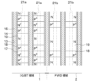
- a stabilization layer 19 is also formed in the IGBT region 1.
- the rest is similar to the first embodiment, a description thereof will be omitted here.
- a stabilization layer 19 is formed in the surface layer of the second base layer 12b together with the emitter region 17 and the contact region 18.
- the surface 10a of the semiconductor substrate 10 in the IGBT region 1 is formed of the emitter region 17, the contact region 18, and the stabilization layer 19.
- the contact region 18, the emitter region 17, the contact region 18, and the stabilization layer 19 are repeatedly formed in this order along the longitudinal direction between adjacent trenches 13. That is, in the IGBT region 1 of this embodiment, the stabilization layer 19 is formed in the surface 10a of the semiconductor substrate 10 in the portion where the second base layer 12b in the first embodiment was exposed.
- the stabilization layer 19 has a lower impurity concentration than the contact region 18.
- the stabilization layer 19 in such a semiconductor device is formed as follows. That is, the stabilization layer 19 is formed by ion implanting N-type impurities after forming the emitter region 17 and the contact region 18 in the surface layer portion of the second base layer 12b. In this case, the impurity concentration of the stabilization layer 19 is lower than that of the contact region 18, so that even if the N-type impurity is ion implanted without placing a mask, the contact region 18 will not be turned back to N-type. Therefore, in this embodiment, by forming the stabilization layer 19 also in the IGBT region 1, the stabilization layer 19 can be formed by ion implanting N-type impurities without placing a mask, and the manufacturing process can be simplified.
- Fig. 7 shows the results when the surface concentration of emitter region 17 is 2.0 x 10²⁰ / cm3 .
- the stabilization layer 19 has a lower impurity concentration than the emitter region 17 in order to prevent a decrease in the latch-up resistance.
- the stabilization layer 19 may affect the threshold voltage Vth (i.e., the gate-emitter voltage Vge) of the IGBT element.
- Vth i.e., the gate-emitter voltage Vge
- the results shown in FIG. 8 were obtained as the relationship between the gate-emitter voltage Vge and the collector current Ic and the peak position of the stabilization layer 19.
- FIG. 8 shows the depth from the surface 10a of the semiconductor substrate 10 to the peak position where the impurity concentration of the stabilization layer 19 is maximum as the peak position of the stabilization layer 19.
- FIG. 8 shows the depth from the surface 10a of the semiconductor substrate 10 to the second peak position P2 of the second base layer 12b as 0.86 ⁇ m.
- the peak position of the stabilization layer 19 in FIG. 8 being 0 means that the stabilization layer 19 is not formed.
- the threshold voltage Vth remains almost unchanged if the peak position where the impurity concentration of the stabilization layer 19 is at its maximum is 0.5 ⁇ m or less. In other words, it has been confirmed that the threshold voltage Vth remains unchanged if the depth from the surface 10a of the semiconductor substrate 10 to the peak position where the impurity concentration of the stabilization layer 19 is at its maximum is 58% or less of the depth from the surface 10a of the semiconductor substrate 10 to the second peak position P2 of the second base layer 12b. Therefore, it is preferable that the stabilization layer 19 has a depth to the peak position where the impurity concentration is at its maximum of 58% or less of the depth from the surface 10a of the semiconductor substrate 10 to the second peak position P2 of the second base layer 12b.
- the FWD region 2 is configured such that one surface 10a of the semiconductor substrate 10 connected to the upper electrode 22 includes an N-type stabilization layer 19. Therefore, the same effect as in the first embodiment can be obtained.
- a stabilization layer 19 is also formed in the IGBT region 1, and the stabilization layer 19 has a lower impurity concentration than the contact region 18. Therefore, the stabilization layer 19 can be formed by ion implantation of N-type impurities without placing a mask, which simplifies the manufacturing process.
- the surface concentration of the stabilization layer 19 is made lower than the surface concentration of the emitter region 17, thereby preventing a decrease in the latch-up resistance.
- the stabilization layer 19 is formed so that the peak position of the stabilization layer 19 relative to the second peak position P2 of the second base layer 12b is 58% or less, thereby suppressing fluctuations in the threshold voltage Vth.
- a semiconductor device in which the first conductivity type is N type and the second conductivity type is P type has been described, but the semiconductor device may also be one in which the first conductivity type is P type and the second conductivity type is N type. Also, in each of the above embodiments, a trench gate structure does not have to be formed in the FWD region 2.
- the stabilization layer 19 may be formed in a part of the surface layer of the second base layer 12b, so that the second base layer 12b is exposed from the surface 10a of the semiconductor substrate 10. Even in such a semiconductor device, the proportion of the second base layer 12b, which is prone to variation in impurity concentration, on the surface 10a of the semiconductor substrate 10 can be reduced compared to a case in which the surface 10a of the semiconductor substrate 10 in the FWD region 2 is formed of the contact region 18 and the second base layer 12b. Therefore, the same effect as in the first embodiment can be obtained.
- one surface 10a of the semiconductor substrate 10 in the IGBT region 1 is formed of the emitter region 17, the contact region 18, and the stabilization layer 19.
- the stabilization layer 19 may be formed in a part of the surface layer of the second base layer 12b in the IGBT region 1, so that the second base layer 12b is exposed from the one surface 10a of the semiconductor substrate 10.
- the stabilization layer 19 may have a surface concentration higher than that of the emitter region 17.
- the stabilization layer 19 may be formed at a depth such that the peak position of the stabilization layer 19 is greater than 58% of the second peak position P2 of the second base layer 12b.
- the proportion of the second base layer 12b, which is prone to impurity concentration variations, on the surface 10a of the semiconductor substrate 10 can be reduced compared to a case in which the surface 10a of the semiconductor substrate 10 in the FWD region 2 is composed of the contact region 18 and the second base layer 12b. Therefore, the same effect as in the first embodiment can be obtained.
- the contact region is also formed in a surface layer portion of the second base layer in the IGBT region;
- the stabilization layer is formed in the FWD region over an entire region of a portion of one surface of the semiconductor substrate different from the contact region, and further formed in the IGBT region over an entire region of a portion of one surface of the semiconductor substrate different from the emitter region and the contact region, and has an impurity concentration lower than that of the contact region.
- a semiconductor device according to a third or fourth aspect, wherein a stabilization layer in the IGBT region has a depth from one surface of the semiconductor substrate to a peak position where the impurity concentration in the stabilization layer is at its maximum that is 58% or less of a depth from one surface of the semiconductor substrate to a peak position where the impurity concentration in the second base layer is at its maximum.
Landscapes
- Electrodes Of Semiconductors (AREA)
Priority Applications (1)
| Application Number | Priority Date | Filing Date | Title |
|---|---|---|---|
| CN202480048650.5A CN121587089A (zh) | 2023-07-25 | 2024-07-23 | 半导体装置 |
Applications Claiming Priority (2)
| Application Number | Priority Date | Filing Date | Title |
|---|---|---|---|
| JP2023121047A JP2025017799A (ja) | 2023-07-25 | 2023-07-25 | 半導体装置 |
| JP2023-121047 | 2023-07-25 |
Publications (1)
| Publication Number | Publication Date |
|---|---|
| WO2025023245A1 true WO2025023245A1 (ja) | 2025-01-30 |
Family
ID=94375356
Family Applications (1)
| Application Number | Title | Priority Date | Filing Date |
|---|---|---|---|
| PCT/JP2024/026322 Pending WO2025023245A1 (ja) | 2023-07-25 | 2024-07-23 | 半導体装置 |
Country Status (3)
| Country | Link |
|---|---|
| JP (1) | JP2025017799A (https=) |
| CN (1) | CN121587089A (https=) |
| WO (1) | WO2025023245A1 (https=) |
Citations (3)
| Publication number | Priority date | Publication date | Assignee | Title |
|---|---|---|---|---|
| JP2010103326A (ja) * | 2008-10-24 | 2010-05-06 | Toyota Motor Corp | Igbt、及び、igbtの製造方法 |
| JP2012231092A (ja) * | 2011-04-27 | 2012-11-22 | Toyota Motor Corp | 半導体装置の製造方法 |
| JP2016115766A (ja) * | 2014-12-12 | 2016-06-23 | 株式会社豊田中央研究所 | 逆導通igbt |
-
2023
- 2023-07-25 JP JP2023121047A patent/JP2025017799A/ja active Pending
-
2024
- 2024-07-23 CN CN202480048650.5A patent/CN121587089A/zh active Pending
- 2024-07-23 WO PCT/JP2024/026322 patent/WO2025023245A1/ja active Pending
Patent Citations (3)
| Publication number | Priority date | Publication date | Assignee | Title |
|---|---|---|---|---|
| JP2010103326A (ja) * | 2008-10-24 | 2010-05-06 | Toyota Motor Corp | Igbt、及び、igbtの製造方法 |
| JP2012231092A (ja) * | 2011-04-27 | 2012-11-22 | Toyota Motor Corp | 半導体装置の製造方法 |
| JP2016115766A (ja) * | 2014-12-12 | 2016-06-23 | 株式会社豊田中央研究所 | 逆導通igbt |
Also Published As
| Publication number | Publication date |
|---|---|
| CN121587089A (zh) | 2026-02-27 |
| JP2025017799A (ja) | 2025-02-06 |
Similar Documents
| Publication | Publication Date | Title |
|---|---|---|
| CN109964317B (zh) | 半导体装置 | |
| JP5605073B2 (ja) | 半導体装置 | |
| CN107210299B (zh) | 半导体装置 | |
| JP7459694B2 (ja) | 半導体装置 | |
| JP7247930B2 (ja) | 半導体装置 | |
| US12363997B2 (en) | Semiconductor device | |
| JP5480084B2 (ja) | 半導体装置 | |
| CN112673466B (zh) | 半导体装置 | |
| KR100906555B1 (ko) | 절연게이트 양극성 트랜지스터 및 그 제조방법 | |
| JP6954333B2 (ja) | 半導体装置 | |
| JP7172920B2 (ja) | 半導体装置 | |
| JP2017195224A (ja) | スイッチング素子 | |
| WO2018198575A1 (ja) | 半導体装置 | |
| WO2025023245A1 (ja) | 半導体装置 | |
| JP2024070605A (ja) | 半導体装置 | |
| JP7596930B2 (ja) | 半導体装置 | |
| KR102607643B1 (ko) | 플로팅 구조를 이용한 rc-igbt | |
| JP7524589B2 (ja) | 半導体装置 | |
| JP2024127086A (ja) | 半導体装置 | |
| WO2025009490A1 (ja) | 半導体装置 | |
| WO2025225266A1 (ja) | 半導体装置および半導体装置の製造方法 | |
| JP2025111861A (ja) | 半導体装置 | |
| JP2004266298A (ja) | 縦型半導体装置 |
Legal Events
| Date | Code | Title | Description |
|---|---|---|---|
| NENP | Non-entry into the national phase |
Ref country code: DE |