WO2025022671A1 - 電力半導体装置 - Google Patents
電力半導体装置 Download PDFInfo
- Publication number
- WO2025022671A1 WO2025022671A1 PCT/JP2023/027643 JP2023027643W WO2025022671A1 WO 2025022671 A1 WO2025022671 A1 WO 2025022671A1 JP 2023027643 W JP2023027643 W JP 2023027643W WO 2025022671 A1 WO2025022671 A1 WO 2025022671A1
- Authority
- WO
- WIPO (PCT)
- Prior art keywords
- heat sink
- semiconductor device
- power semiconductor
- air flow
- power
- Prior art date
- Legal status (The legal status is an assumption and is not a legal conclusion. Google has not performed a legal analysis and makes no representation as to the accuracy of the status listed.)
- Pending
Links
Images












Classifications
-
- H—ELECTRICITY
- H05—ELECTRIC TECHNIQUES NOT OTHERWISE PROVIDED FOR
- H05K—PRINTED CIRCUITS; CASINGS OR CONSTRUCTIONAL DETAILS OF ELECTRIC APPARATUS; MANUFACTURE OF ASSEMBLAGES OF ELECTRICAL COMPONENTS
- H05K7/00—Constructional details common to different types of electric apparatus
- H05K7/20—Modifications to facilitate cooling, ventilating, or heating
- H05K7/2089—Modifications to facilitate cooling, ventilating, or heating for power electronics, e.g. for inverters for controlling motor
- H05K7/209—Heat transfer by conduction from internal heat source to heat radiating structure
-
- H—ELECTRICITY
- H10—SEMICONDUCTOR DEVICES; ELECTRIC SOLID-STATE DEVICES NOT OTHERWISE PROVIDED FOR
- H10W—GENERIC PACKAGES, INTERCONNECTIONS, CONNECTORS OR OTHER CONSTRUCTIONAL DETAILS OF DEVICES COVERED BY CLASS H10
- H10W40/00—Arrangements for thermal protection or thermal control
- H10W40/20—Arrangements for cooling
- H10W40/231—Arrangements for cooling characterised by their places of attachment or cooling paths
- H10W40/235—Arrangements for cooling characterised by their places of attachment or cooling paths attached to package parts
-
- H—ELECTRICITY
- H10—SEMICONDUCTOR DEVICES; ELECTRIC SOLID-STATE DEVICES NOT OTHERWISE PROVIDED FOR
- H10W—GENERIC PACKAGES, INTERCONNECTIONS, CONNECTORS OR OTHER CONSTRUCTIONAL DETAILS OF DEVICES COVERED BY CLASS H10
- H10W40/00—Arrangements for thermal protection or thermal control
- H10W40/40—Arrangements for thermal protection or thermal control involving heat exchange by flowing fluids
- H10W40/43—Arrangements for thermal protection or thermal control involving heat exchange by flowing fluids by flowing gases, e.g. forced air cooling
Definitions
- This disclosure relates to a power semiconductor device equipped with a heat sink and a power module.
- the power semiconductor device disclosed in Patent Document 1 comprises a base, a heat sink having a number of fins arranged in parallel at intervals on one side of the base, and a number of power semiconductor modules arranged on the other side of the base.
- the power semiconductor device described in Patent Document 1 reduces the temperature rise of the power semiconductor modules by blowing cooling air along the row of fins of the heat sink.
- the multiple power semiconductor modules are aligned diagonally with respect to the flow direction of the cooling air so that the power semiconductor modules on the downwind side are not affected by the heat generated by the power semiconductor modules on the upwind side.
- the present disclosure has been made in consideration of the above, and aims to obtain a power semiconductor device in which the power semiconductor module on the downwind side is less susceptible to the effects of heat generated by the power semiconductor module on the upwind side.
- the power semiconductor device comprises a housing having an air passage formed with an inlet and an outlet for the air flow facing each other, a flat heat sink base, and a plurality of flat fins arranged in parallel at intervals on one surface of the heat sink base, a heat sink held in the housing with the plurality of fins arranged in the air passage, and a plurality of power modules arranged on the other surface of the heat sink base.
- An uneven surface is formed on the other surface of the heat sink base.
- the power modules have uneven portions that fit into the uneven surface of the heat sink base, and the uneven portions are fitted into the uneven surface of the heat sink base and are arranged at intervals along the traveling direction of the air flow, and one power module adjacent to the traveling direction of the air flow is offset relative to the other adjacent power module in a direction perpendicular to the traveling direction of the air flow.
- the power semiconductor device disclosed herein has the advantage that the power semiconductor module on the downwind side is less susceptible to the effects of heat generated by the power semiconductor module on the upwind side.
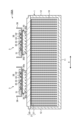
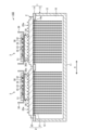
- FIG. 1 is a plan view showing a power semiconductor device according to a first embodiment
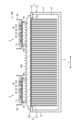
- FIG. 2 is a cross-sectional view taken along the line II-II in FIG. 3 is a cross-sectional view taken along the line III-III in FIG.
- FIG. 1 is a plan view showing a power semiconductor device according to a first comparative example
- 5 is a cross-sectional view taken along the line V-V in FIG.
- FIG. 1 is a contour diagram showing the temperature distribution of air flowing from the inlet to the outlet in the power semiconductor device of Comparative Example 1.
- FIG. 1 is a contour diagram showing a temperature distribution of air flowing from an inlet to an outlet in a power semiconductor device according to a first embodiment
- FIG. 11 is a plan view showing a power semiconductor device according to a second comparative example. IX-IX arrow cross-sectional view shown in FIG. 8 XX arrow cross-sectional view shown in FIG.
- FIG. 1 is a plan view showing a first modification of the uneven surface of the power semiconductor device according to the first embodiment;
- FIG. 1 is a plan view showing a second modified example of the uneven surface of the power semiconductor device according to the first embodiment;
- FIG. 1 is a plan view showing a third modification of the uneven surface of the power semiconductor device according to the first embodiment;
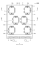
- FIG. 11 is a plan view showing a power semiconductor device according to a second embodiment;
- 15 is a cross-sectional view taken along the line XV-XV in FIG.
- FIG. 16 is a cross-sectional view taken along the line XVI-XVI in FIG.
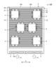
- FIG. 11 is a plan view showing a mounting plate of a power semiconductor device according to a second embodiment
- FIG. 11 is a plan view showing a power semiconductor device according to a third embodiment.
- 19 is a cross-sectional view taken along the line XIX-XIX in FIG.
- FIG. 13 is a plan view showing a mounting plate of the power semiconductor device according to the third embodiment
- FIG. 13 is a plan view showing a modification of the power semiconductor device according to the third embodiment
- FIG. 13 is a plan view showing a mounting plate of a modified example of the power semiconductor device according to the third embodiment
- FIG. 13 is a vertical cross-sectional view showing a schematic diagram of a power semiconductor device according to a fourth embodiment of the present invention
- FIG. 13 is a vertical cross-sectional view showing a first modified example of the power semiconductor device according to the fourth embodiment
- FIG. 13 is a vertical cross-sectional view showing a schematic diagram of a second modified example of the power semiconductor device according to the fourth embodiment
- Fig. 1 is a plan view of a power semiconductor device according to a first embodiment.
- the outline arrows in Fig. 1 indicate the direction of travel of air flow A.
- Fig. 2 is a cross-sectional view taken along line II-II in Fig. 1.
- Fig. 3 is a cross-sectional view taken along line III-III in Fig. 1. Note that some hatching has been omitted from the cross-sectional views in order to make it easier to see the components of the power module 3.
- the power semiconductor device 100 includes a housing 1, a heat sink 2, a plurality of power modules 3, and a cooling fan 4.
- the housing 1 forms an air passage 10 in which the inlet 10a and outlet 10b of the air flow A face each other, and holds a heat sink-integrated power module in which a heat sink 2 and a plurality of power modules 3 are integrated.
- the housing 1 is concave with a bottom surface 11 and a pair of side surfaces 12. Both ends of the housing 1 extending along the traveling direction of the air flow A are open, with one open end being the inlet 10a of the air flow A and the other open end being the outlet 10b of the air flow A.
- the air passage 10 is a space surrounded by the bottom surface 11 and the pair of side surfaces 12. In the example shown in Fig.
- the traveling direction of the air flow A is from the inlet 10a to the outlet 10b, but this is not limited thereto, and the air flow may be in the reverse direction from the outlet 10b to the inlet 10a, with the outlet 10b being the inlet and the inlet 10a where the cooling fan 4 is arranged being the outlet.
- the housing 1 is made of plated steel. Plated steel is a material that is rigid enough to hold a heat sink-integrated power module and can be made thin and lightweight.
- the housing 1 may be made of a material other than plated steel.
- the heat sink 2 is integrated with the multiple power modules 3 and dissipates heat generated by the power modules 3.
- the heat sink 2 has a flat heat sink base 20 and multiple flat fins 21 arranged in parallel and spaced apart on one surface of the heat sink base 20.
- the heat sink 2 is a crimped heat sink in which the heat sink base 20 and the fins 21 are integrated by "crimping.”
- the heat sink 2 is held in the housing 1 with the multiple fins 21 arranged in the air passage 10.
- the heat sink base 20 is rectangular, for example.
- the heat sink base 20 is made of a metal material with relatively high thermal conductivity so that heat generated by the power module 3 can be efficiently transferred to the fins 21.
- the heat sink base 20 is made of a metal material that is resistant to corrosion, such as aluminum or an aluminum alloy, for example.
- the heat sink base 20 is manufactured by a processing method such as cutting, die casting, forging, or extrusion.
- the other side of the heat sink base 20 has an uneven surface 20a formed in one area where the multiple power modules 3 are provided, with recesses and protrusions extending along the direction of travel of the air flow A.
- One area where the multiple power modules 3 are provided is, as an example, the entire surface of the other side of the heat sink base 20.
- the heat sink base 20, with multiple fins 21 housed inside the concave-shaped housing 1, has its outer periphery placed on the upper end surface of the side portion 12 and is fixed to the side portion 12 with a joining member (not shown) such as a screw.
- the side portion 12 is provided with a screw hole (not shown) for inserting a screw or the like.
- the heat sink base 20 is also provided with a screw hole or through hole (not shown) at a position corresponding to the screw hole provided in the side portion 12.
- the fins 21 are heat dissipation components made of thin rectangular plates.
- the fins 21 are made of a metal material with relatively high thermal conductivity so that they can dissipate heat generated by the power module 3.
- the fins 21 are made of a metal material that is resistant to corrosion, such as aluminum or an aluminum alloy. By using a rolled material of a metal material such as aluminum for the fins 21, it is possible to achieve both workability and heat dissipation properties for the fins 21.
- Each of the multiple fins 21 is inserted into a fin insertion groove (not shown) formed on one surface of the heat sink base 20 and is fixed to the heat sink base 20 by crimping.
- the heat sink 2 is a crimped heat sink, there are no processing restrictions on aspect ratio in die casting and extrusion, so the fins 21 can be designed freely and the heat dissipation capacity can be improved.
- the heat sink 2 is not limited to a crimped heat sink and may be made by other processing methods.
- the heat sink 2 may be made by integrally manufacturing the fins 21 and the heat sink base 20 by extrusion or die casting.
- a heat sink 2 made by cutting or forging may be used.
- the power module 3 is a power semiconductor module and is of a resin molded type. As shown in FIG. 1, a plurality of power modules 3 are provided at intervals along the traveling direction of the air flow A. In the power semiconductor device 100 shown in FIG. 1, as an example, six power modules 3 arranged in two columns and three rows are mounted. Note that the number of power modules 3 is not limited to the six shown in the figure, and it is sufficient that there are two or more power modules 3 spaced apart along the traveling direction of the air flow A.
- one of the power modules 3 adjacent to each other in the traveling direction of the air flow A is offset in a direction X perpendicular to the traveling direction of the air flow A relative to the other adjacent power module 3.
- the middle power module 3 is offset in a direction X perpendicular to the traveling direction of the air flow A relative to the windwardest power module 3 and the leewardest power module 3.
- the power module 3 includes a fin base 30, an insulating material 31, a metal conductor 32, a semiconductor element 33, a bonding material 34, a wiring wire 35, a control terminal 36, a main terminal 37, and a sealing material 38.
- the fin base 30 is a rectangular flat plate smaller than the heat sink base 20, and is a connection part for connecting the power module 3 to the heat sink 2.
- the fin base 30 is made of a metal material with relatively high thermal conductivity so that heat generated by the power module 3 can be efficiently transferred to the heat sink 2.
- the fin base 30 is made of a metal material that is resistant to corrosion, such as aluminum or an aluminum alloy.
- the fin base 30 is manufactured by a processing method such as cutting, die casting, forging, or extrusion.
- the fin base 30 has an uneven portion 30a formed on one surface facing the heat sink base 20, which fits into the uneven surface 20a of the heat sink base 20.
- the power module 3 is integrated with the heat sink 2 by fitting the uneven portion 30a of the fin base 30 and the uneven surface 20a of the heat sink base 20 by press processing.
- the power module 3 is freely arranged and installed within the area where the uneven surface 20a is formed.
- the power module 3 is a greaseless power module in which no thermally conductive grease is used between the power module 3 and the heat sink 2.
- Greaseless power modules can improve the heat dissipation performance of the heat generated in the power module 3 compared to power modules using thermally conductive grease, so they are suitable for use in power semiconductor devices with large power capacities.
- in the power semiconductor device 100 when replacing the power module 3, since no thermally conductive grease is used, there is no need to remove and relocate the thermally conductive grease, which improves productivity and maintainability.
- the materials of the heat sink base 20, the fins 21, and the fin base 30 are not limited to the aluminum-based materials described above, and may be other materials.
- the material combination of the heat sink base 20, the fins 21, and the fin base 30 may be a combination of materials different from those described above.
- the heat dissipation capability of the fins 21 is further improved compared to when the fins 21 are plate components made of an aluminum-based material.
- the insulating material 31 is an insulating sheet with heat dissipation properties.
- the insulating material 31 is fixed to the other side of the fin base 30.
- the insulating material 31 insulates the components of the power module 3 sealed by the sealing material 38 from the heat sink base 20, and dissipates heat generated by the semiconductor element 33 to the heat sink base 20.
- the insulating material 31 has heat dissipation properties equal to or greater than those of the sealing material 38.
- the metal conductor 32 is a substrate on which the semiconductor element 33 is mounted, and dissipates heat generated by the semiconductor element 33 to the insulating material 31.
- the semiconductor element 33 is a semiconductor element for power control.
- Examples of the semiconductor element 33 are a rectifier diode, a power transistor, a thyristor, and an IGBT (Insulated Gate Bipolar Transistor).
- the semiconductor element 33 is exemplified by an element formed of silicon (Si), or an element formed of a wide band gap semiconductor having a larger band gap than silicon. Examples of wide band gap semiconductors are silicon carbide (SiC), gallium nitride-based materials, and diamond.
- the semiconductor element 33 using a wide band gap semiconductor has a high allowable current density and low power loss, so that the power module 3 can be made smaller, and thus the heat sink 2 and the power semiconductor device 100 can be made smaller.
- the bonding material 34 is, for example, solder, and bonds the metal conductor 32 and the semiconductor element 33.
- the semiconductor element 33 is die-bonded to the metal conductor 32 using the bonding material 34.
- the bonding material 34 is not limited to solder, and may have other configurations.
- the wiring wires 35 electrically connect the semiconductor elements 33 to each other.
- the wiring wires 35 also electrically connect the semiconductor elements 33 to the main terminals 37.
- the control terminal 36 and the main terminal 37 are connected to the semiconductor element 33 to supply power to the semiconductor element 33 or transmit signals between the semiconductor element 33 and an external device.
- the sealing material 38 is formed from a thermosetting resin such as epoxy, and ensures insulation between the components of the power module 3.
- the sealing material 38 is a transfer mold formed by transfer molding, for example.
- the sealing material 38 is not limited to a thermosetting resin.
- the molding method of the sealing material 38 is not limited to transfer molding.
- the cooling fan 4 generates an air flow A that flows from the inlet 10a of the housing 1 to the outlet 10b.
- the cooling fan 4 is provided at the inlet 10a of the housing 1.
- the cooling fan 4 can be attached to the housing 1 by providing a fan mounting structure on a part of the housing 1 and attaching the cooling fan 4 thereto, or by providing a mounting member separate from the housing 1 at the inlet 10a and attaching the cooling fan 4 thereto.
- FIG. 4 is a plan view showing the power semiconductor device of Comparative Example 1.
- FIG. 5 is a cross-sectional view taken along the line V-V shown in FIG. 4.
- FIG. 6 is a contour diagram showing the temperature distribution of air flowing from the inlet to the outlet in the power semiconductor device of Comparative Example 1.
- multiple power modules 3 are provided at intervals along the direction of air flow A.
- the power modules 3 are arranged in 2 columns and 3 rows, aligned along the direction of air flow A.
- the temperature of the air flowing between the fins 21 of the heat sink 2 from the upwind side to the downwind side increases continuously.
- the semiconductor element 33 of the downwind power module 3 is affected by the heat generated by the semiconductor element 33 of the upwind power module 3, and the temperature of the downwind power module 3 increases due to thermal interference.
- one of the power modules 3 adjacent to each other in the traveling direction of the air flow A is offset in a direction X perpendicular to the traveling direction of the air flow A relative to the other adjacent power module 3.
- the middle power module 3 is offset in a direction X perpendicular to the traveling direction of the air flow A relative to the windwardest power module 3 and the leewardest power module 3.
- FIG. 7 is a contour diagram showing the temperature distribution of air flowing from the inlet to the outlet in the power semiconductor device of the first embodiment.
- the power semiconductor device 100 of the first embodiment can reduce cumulative thermal interference, so that the semiconductor element 33 of the power module 3 on the downwind side is less susceptible to the effects of heat generated from the semiconductor element 33 of the power module 3 on the upwind side, and low-temperature air can be sent to the downwind side. Therefore, the power semiconductor device 100 of the first embodiment can effectively suppress the temperature rise of the power module 3.
- FIG. 8 is a plan view showing a power semiconductor device of Comparative Example 2.
- FIG. 9 is a cross-sectional view taken along the line IX-IX shown in FIG. 8.
- FIG. 10 is a cross-sectional view taken along the line X-X shown in FIG. 8.
- each power module 3 has a fin base 30 on which uneven portions 30a that fit into the uneven surface 20a of the heat sink base 20 are formed.
- the position of the power module 3 to be installed on the heat sink base 20 is determined at the design stage of the uneven surface 20a, so if it becomes necessary to change the position of the power module 3 after the design, a new heat sink base 20 must be produced.
- an uneven surface 20a is formed on the other surface of the heat sink base 20.
- the power module 3 has a fin base 30 on which an uneven portion 30a that fits into the uneven surface 20a of the heat sink base 20 is formed.
- the power module 3 can be freely positioned within the area in which the uneven surface 20a of the heat sink base 20 is formed, so there is a high degree of freedom in design and the productivity of the heat sink integrated power module can be increased.
- FIG. 11 is a plan view showing a first modified uneven surface of the power semiconductor device according to the first embodiment.
- FIG. 12 is a plan view showing a second modified uneven surface of the power semiconductor device according to the first embodiment.
- FIG. 13 is a plan view showing a third modified uneven surface of the power semiconductor device according to the first embodiment.
- the uneven surface 20a of the heat sink base 20 is not limited to a configuration in which the recesses and protrusions extend along the direction of travel of the air flow A as shown in FIG. 1. As shown in FIG. 11, the uneven surface 20a may be configured so that the recesses and protrusions extend along a direction intersecting the direction of travel of the air flow A, such as a direction perpendicular to the direction of travel of the air flow A.
- the recesses and protrusions are not limited to the configuration in which they are continuously formed as shown in FIG. 1, but may be configured to be intermittently formed along the extending direction as shown in FIG. 12.
- the uneven surface 20a may be configured, for example, so that dot-shaped protrusions are aligned, or may have other configurations.
- the uneven surface 20a only needs to be configured to fit the uneven portion 30a of the power module 3, and the shape of the recesses and protrusions, the orientation of the recesses and protrusions, and the range in which the recesses and protrusions are formed can be appropriately changed according to the configuration of the power semiconductor device 100.
- the uneven portion 30a of the power module 3 is formed to match the configuration of the uneven surface 20a.
- Fig. 14 is a plan view showing the power semiconductor device according to the second embodiment.
- Fig. 15 is a cross-sectional view taken along the line XV-XV shown in Fig. 14.
- Fig. 16 is a cross-sectional view taken along the line XVI-XVI shown in Fig. 14.
- Fig. 17 is a plan view showing a mounting plate of the power semiconductor device according to the second embodiment. Note that some hatching has been omitted from the cross-sectional view in order to make it easier to see the components of the power module 3.
- the housing 1 of the power semiconductor device 101 has a configuration in which a plurality of openings 14a are formed at intervals along the direction of travel of the air flow A on one side that forms the air passage 10.
- the housing 1 has a concave-shaped housing 13 formed of a bottom surface portion 11 and a pair of side surfaces 12, and an attachment plate 14 that is disposed opposite the bottom surface portion 11 and covers the opening surface of the housing 13.
- the housing 1 is formed into a rectangular tube by the housing 13 and the attachment plate 14. Both ends of the housing 1 that extend along the direction of travel of the air flow A are open, with one open end serving as an inlet 10a for the air flow A blown from the cooling fan 4, and the other open end serving as an outlet 10b for the air flow A.
- the air passage 10 is a space surrounded by the housing 13 and the attachment plate 14.
- the direction of travel of the air flow A is from the inlet 10a to the outlet 10b, but this is not limited thereto.
- the air flow A may travel in the opposite direction, from the outlet 10b to the inlet 10a, with the outlet 10b serving as the inlet and the inlet 10a where the cooling fan 4 is located serving as the outlet.
- the housing 13 and mounting plate 14 are made of plated steel.
- Plated steel is a material that has the rigidity to hold the heat sink-integrated power module and can be made thin and lightweight.
- the housing 13 and mounting plate 14 may be made of a material other than plated steel.
- the outer peripheral edge of the mounting plate 14 is placed on the upper end surface of the side portion 12, and is fixed to the side portion 12 with a connecting member (not shown) such as a screw.
- the side portion 12 is provided with a screw hole (not shown) for screwing in a connecting member such as a screw.
- the mounting plate 14 is also provided with a screw hole or through hole (not shown) at a position corresponding to the screw hole provided in the side portion 12.
- the mounting plate 14 has three openings 14a of the same shape and size aligned at intervals along the direction of air flow A.
- the openings 14a are rectangular in shape that is long in the direction X perpendicular to the direction of air flow A when the power semiconductor device 101 is viewed in plan.
- the heat sink 2 is provided in individual pieces for each opening 14a, and as shown in FIGS. 15 and 16, the fins 21 are fitted through the openings 14a and supported by the housing 1 in the air passage 10.
- the heat sink 2 is formed to match the size and shape of the openings 14a.
- the heat sink base 20 is placed on the upper surface of the mounting plate 14 at its outer periphery and fixed to the mounting plate 14 with a joining member such as a screw (not shown).
- the mounting plate 14 is provided with screw holes (not shown) for screwing in joining members such as a screw.
- the heat sink base 20 is also provided with screw holes or through holes (not shown) at positions corresponding to the screw holes provided in the mounting plate 14.
- the power semiconductor device 101 according to the second embodiment has a configuration in which the heat sink 2 is partially omitted compared to the configuration of the first embodiment, and therefore the weight of the device can be reduced. Furthermore, in the case where a power module 3 fails, the power semiconductor device 101 according to the second embodiment only requires replacing the heat sink 2 on which the failed power module 3 is mounted, improving maintainability.
- one of the power modules 3 adjacent to each other in the traveling direction of the air flow A is offset in the direction X perpendicular to the traveling direction of the air flow A relative to the other adjacent power module 3.
- the middle power module 3 is offset in the direction X perpendicular to the traveling direction of the air flow A relative to the windward-most power module 3 and the leeward-most power module 3.
- the power semiconductor device 101 according to the second embodiment can reduce cumulative thermal interference, so that the semiconductor elements 33 of the power module 3 on the downwind side are less susceptible to the effects of heat generated by the semiconductor elements 33 of the power module 3 on the upwind side, and low-temperature air can be sent to the downwind side. Therefore, the power semiconductor device 101 according to the second embodiment can effectively suppress the temperature rise of the power module 3.
- the power semiconductor device 101 allows the power module 3 to be freely positioned within the area in which the uneven surface 20a of the heat sink base 20 is formed, allowing for a high degree of freedom in design and improving the productivity of the heat sink-integrated power module.
- the housing 13 and the mounting plate 14 are formed as separate members and then joined together, but they may be integrally molded as one member.
- the number of openings 14a is not limited to three as shown in the figure, and may be two, four or more.
- the shape of the openings 14a is not limited to a rectangular shape that is long in the direction X perpendicular to the direction of air flow A, and may be another shape such as a square, or may be a rectangular shape that is long along the direction of air flow A.
- the number of power modules 3 provided on one individualized heat sink 2 is not limited to two as shown in the figure, and may be one, or three or more.
- Fig. 18 is a plan view showing the power semiconductor device according to the third embodiment.
- Fig. 19 is a cross-sectional view taken along the line XIX-XIX shown in Fig. 18.
- Fig. 20 is a plan view showing a mounting plate of the power semiconductor device according to the third embodiment.
- the housing 1 of the power semiconductor device 102 has a configuration in which a plurality of openings 14a are formed at intervals along the direction of travel of the air flow A on one side that forms the air passage 10.
- the housing 1 has a concave-shaped housing 13 formed of a bottom surface portion 11 and a pair of side surfaces 12, and an attachment plate 14 that is disposed opposite the bottom surface portion 11 and covers the opening surface of the housing 13.
- the housing 1 is formed into a rectangular tube by the housing 13 and the attachment plate 14.
- Both ends of the housing 1 that extend along the direction of travel of the air flow A are open, with one open end serving as an inlet 10a for the air flow A blown from the cooling fan 4, and the other open end serving as an outlet 10b for the air flow A.
- the air passage 10 is a space surrounded by the housing 13 and the attachment plate 14.
- the direction of travel of the air flow A is from the inlet 10a to the outlet 10b, but this is not limited thereto.
- the air flow A may travel in the opposite direction, from the outlet 10b to the inlet 10a, with the outlet 10b serving as the inlet and the inlet 10a where the cooling fan 4 is located serving as the outlet.
- the housing 13 and mounting plate 14 are made of plated steel plate.
- Plated steel plate is a material that has the rigidity to hold the heat sink 2 with multiple power modules 3 integrated into it, and can be made thin and lightweight.
- the housing 13 and mounting plate 14 may be made of a material other than plated steel plate.
- the outer peripheral edge of the mounting plate 14 is placed on the upper end surface of the side portion 12, and is fixed to the side portion 12 with a connecting member (not shown) such as a screw.
- the side portion 12 is provided with a screw hole (not shown) for screwing in a connecting member such as a screw.
- the mounting plate 14 is also provided with a screw hole or through hole (not shown) at a position corresponding to the screw hole provided in the side portion 12.
- the mounting plate 14 has a plurality of openings 14a formed at intervals along the traveling direction of the air flow A.
- the plurality of openings 14a are arranged in a plurality of rows.
- the openings 14a are arranged in, for example, two columns and three rows, and are aligned along the traveling direction of the air flow A.
- the openings 14a are, for example, rectangular in shape that is long in the direction X perpendicular to the traveling direction of the air flow A.
- the heat sink 2 is provided as an individual piece for each opening 14a, and as shown in FIG. 19, the fins 21 are fitted through the openings 14a and supported by the housing 1 in a state in which they are arranged in the air passage 10.
- the heat sink 2 is formed to match the size and shape of the openings 14a.
- the outer edge of the heat sink base 20 is placed on the upper surface of the mounting plate 14 and fixed to the mounting plate 14 with a joining member such as a screw (not shown).
- the mounting plate 14 is provided with a screw hole (not shown) for screwing in a joining member such as a screw.
- the heat sink base 20 is also provided with a screw hole or through hole (not shown) at a position corresponding to the screw hole provided in the mounting plate 14.
- Each of the individual heat sinks 2 is integrated with a power module 3. That is, the power semiconductor device 102 according to the third embodiment has a configuration in which the heat sink 2 is partially omitted compared to the configuration of the first embodiment, and therefore the weight of the device can be reduced. Furthermore, in the case of the power semiconductor device 102 according to the third embodiment, when a power module 3 fails, it is only necessary to replace the heat sink 2 on which the failed power module 3 is mounted, improving maintainability.
- one of the power modules 3 adjacent to each other in the traveling direction of the air flow A is offset from the other adjacent power module 3 in the direction X perpendicular to the traveling direction of the air flow A.
- the middle power module 3 is offset from the windwardest power module 3 and the leewardest power module 3 in the direction X perpendicular to the traveling direction of the air flow A.
- the power semiconductor device 102 according to the third embodiment can reduce cumulative thermal interference, so that the semiconductor elements 33 of the power module 3 on the downwind side are less susceptible to the effects of heat generated by the semiconductor elements 33 of the power module 3 on the upwind side, and low-temperature air can be sent to the downwind side. Therefore, the power semiconductor device 102 according to the third embodiment can effectively suppress the temperature rise of the power module 3.
- the power semiconductor device 102 allows the power module 3 to be freely positioned within the area in which the uneven surface 20a of the heat sink base 20 is formed, allowing for a high degree of design freedom and improving the productivity of the heat sink-integrated power module.
- FIG. 21 is a plan view showing a modified example of the power semiconductor device according to the third embodiment.
- FIG. 22 is a plan view showing a mounting plate of the modified example of the power semiconductor device according to the third embodiment.
- the power semiconductor device 102A shown in FIGS. 21 and 22 has a configuration in which one of the openings 14a adjacent to each other in the traveling direction of the air flow A is offset in a direction X perpendicular to the traveling direction of the air flow A relative to the other adjacent opening 14a. Specifically, of the three openings 14a formed along the inlet 10a and outlet 10b, the opening 14a located in the middle is offset in a direction X perpendicular to the traveling direction of the air flow A relative to the windward opening 14a and the leeward opening 14a.
- FIG. 23 is a vertical cross-sectional view showing the power semiconductor device according to the fourth embodiment.
- the power semiconductor device 103 according to the fourth embodiment differs from the configuration of the bottom surface 11 of the housing 1 described in the second and third embodiments in the configuration. The other configurations are the same as those described in the second or third embodiment.
- the housing 1 in the fourth embodiment has a surface forming the air passage 10, on which a plurality of openings 14a are formed at intervals along the traveling direction of the air flow A.
- the heat sink 2 is provided as individual pieces for each opening 14a, and is supported by the housing 1 in a state in which the fins 21 are fitted from the openings 14a and arranged in the air passage 10.
- the housing 1 has an inclined surface 11a formed on the bottom surface 11 facing the fins 21 of the heat sink 2, which approaches the fins 21 from the inlet 10a forming one end of the direction of travel of the air flow A toward the outlet 10b forming the other end.
- the inclined surface 11a is formed from the inlet 10a to just before the heat sink integrated power module on the most downwind side, and thereafter to the outlet 10b, a horizontal surface 11b extending parallel to the fins 21.
- the air passage 10 is configured in such a shape that the cross-sectional area becomes smaller from the upwind side to the downwind side, the cross-sectional area becomes a minimum just before the heat sink integrated power module on the most downwind side, and the same cross-sectional area is maintained from there to the outlet 10b.
- the horizontal surface 11b does not need to be strictly horizontal, and may be slightly inclined as long as it is approximately horizontal.
- the air flow B which flows between the bottom surface portion 11 and the fins 21 and has almost no temperature rise, can be made to flow in large amounts between the fins 21 of the heat sink 2 located on the downwind side, and the temperature rise of the power module 3 located on the downwind side can be effectively reduced.
- the inclined surface 11a is not limited to a configuration formed from the inlet 10a to just before the heat sink-integrated power module on the most downwind side, but may be formed up to just before the heat sink-integrated power module located in the middle.
- the inclined surface 11a may be formed continuously from the inlet 10a to the outlet 10b, for example, or may be configured to be inclined in stages in combination with the horizontal surface 11b.
- FIG. 24 is a vertical cross-sectional view showing a first modified example of a power semiconductor device according to the fourth embodiment.
- a slope 11a is formed on the bottom surface 11 facing the fins 21 of the heat sink 2, approaching the fins 21 from the outlet 10b forming one end side in the traveling direction of the air flow A toward the inlet 10a forming the other end side.
- the direction of the air flow A in the power semiconductor device 103A shown in FIG. 24 is opposite to that in the power semiconductor device 103 shown in FIG. 23.
- FIG. 25 is a vertical cross-sectional view showing a schematic diagram of modified example 2 of the power semiconductor device according to the fourth embodiment.
- the power semiconductor device 103B shown in FIG. 25 applies the features of the fourth embodiment described with reference to FIG. 23 to the configuration of the first embodiment. That is, the power semiconductor device 103B has a configuration in which a single heat sink 2 is provided with multiple power modules 3, and an inclined surface 11a is formed on the bottom surface 11 of the housing 1. Although not shown, the inclined surface 11a of the power semiconductor device 103A shown in FIG. 24 may be applied to the configuration of the first embodiment.
Landscapes
- Engineering & Computer Science (AREA)
- Microelectronics & Electronic Packaging (AREA)
- Physics & Mathematics (AREA)
- Thermal Sciences (AREA)
- Cooling Or The Like Of Semiconductors Or Solid State Devices (AREA)
Priority Applications (4)
| Application Number | Priority Date | Filing Date | Title |
|---|---|---|---|
| PCT/JP2023/027643 WO2025022671A1 (ja) | 2023-07-27 | 2023-07-27 | 電力半導体装置 |
| CN202380099901.8A CN121400138A (zh) | 2023-07-27 | 2023-07-27 | 电力半导体装置 |
| US19/486,045 US20260113911A1 (en) | 2023-07-27 | 2023-07-27 | Power semiconductor device |
| JP2023577463A JP7479580B1 (ja) | 2023-07-27 | 2023-07-27 | 電力半導体装置 |
Applications Claiming Priority (1)
| Application Number | Priority Date | Filing Date | Title |
|---|---|---|---|
| PCT/JP2023/027643 WO2025022671A1 (ja) | 2023-07-27 | 2023-07-27 | 電力半導体装置 |
Publications (1)
| Publication Number | Publication Date |
|---|---|
| WO2025022671A1 true WO2025022671A1 (ja) | 2025-01-30 |
Family
ID=90926143
Family Applications (1)
| Application Number | Title | Priority Date | Filing Date |
|---|---|---|---|
| PCT/JP2023/027643 Pending WO2025022671A1 (ja) | 2023-07-27 | 2023-07-27 | 電力半導体装置 |
Country Status (4)
| Country | Link |
|---|---|
| US (1) | US20260113911A1 (https=) |
| JP (1) | JP7479580B1 (https=) |
| CN (1) | CN121400138A (https=) |
| WO (1) | WO2025022671A1 (https=) |
Families Citing this family (2)
| Publication number | Priority date | Publication date | Assignee | Title |
|---|---|---|---|---|
| WO2025243727A1 (ja) * | 2024-05-22 | 2025-11-27 | 三菱電機株式会社 | 電力半導体装置、及び、電力変換装置 |
| KR20260009027A (ko) | 2024-07-10 | 2026-01-19 | 엘에스일렉트릭(주) | 히트 싱크 구조체 |
Citations (5)
| Publication number | Priority date | Publication date | Assignee | Title |
|---|---|---|---|---|
| JP2008263137A (ja) * | 2007-04-13 | 2008-10-30 | Nippon Inter Electronics Corp | 冷却装置 |
| JP2011066123A (ja) * | 2009-09-16 | 2011-03-31 | Fuji Electric Systems Co Ltd | 空冷式パワー半導体装置 |
| WO2013157467A1 (ja) * | 2012-04-16 | 2013-10-24 | 富士電機株式会社 | 半導体装置および半導体装置用冷却器 |
| WO2022265003A1 (ja) * | 2021-06-18 | 2022-12-22 | 三菱電機株式会社 | パワー半導体装置およびその製造方法ならびに電力変換装置 |
| JP7258269B1 (ja) * | 2022-10-13 | 2023-04-14 | 三菱電機株式会社 | 電力半導体装置および電力半導体装置の製造方法 |
-
2023
- 2023-07-27 CN CN202380099901.8A patent/CN121400138A/zh active Pending
- 2023-07-27 US US19/486,045 patent/US20260113911A1/en active Pending
- 2023-07-27 JP JP2023577463A patent/JP7479580B1/ja active Active
- 2023-07-27 WO PCT/JP2023/027643 patent/WO2025022671A1/ja active Pending
Patent Citations (5)
| Publication number | Priority date | Publication date | Assignee | Title |
|---|---|---|---|---|
| JP2008263137A (ja) * | 2007-04-13 | 2008-10-30 | Nippon Inter Electronics Corp | 冷却装置 |
| JP2011066123A (ja) * | 2009-09-16 | 2011-03-31 | Fuji Electric Systems Co Ltd | 空冷式パワー半導体装置 |
| WO2013157467A1 (ja) * | 2012-04-16 | 2013-10-24 | 富士電機株式会社 | 半導体装置および半導体装置用冷却器 |
| WO2022265003A1 (ja) * | 2021-06-18 | 2022-12-22 | 三菱電機株式会社 | パワー半導体装置およびその製造方法ならびに電力変換装置 |
| JP7258269B1 (ja) * | 2022-10-13 | 2023-04-14 | 三菱電機株式会社 | 電力半導体装置および電力半導体装置の製造方法 |
Also Published As
| Publication number | Publication date |
|---|---|
| CN121400138A (zh) | 2026-01-23 |
| JP7479580B1 (ja) | 2024-05-08 |
| US20260113911A1 (en) | 2026-04-23 |
| JPWO2025022671A1 (https=) | 2025-01-30 |
Similar Documents
| Publication | Publication Date | Title |
|---|---|---|
| US7190581B1 (en) | Low thermal resistance power module assembly | |
| JP5729374B2 (ja) | 半導体モジュール及び放熱部材 | |
| JP4586087B2 (ja) | パワー半導体モジュール | |
| JP5432085B2 (ja) | 電力半導体装置 | |
| JP7479580B1 (ja) | 電力半導体装置 | |
| US20200035899A1 (en) | Thermoelectric device having circuitry with structural rigidity | |
| US20200388557A1 (en) | Heat transfer for power modules | |
| WO2018146933A1 (ja) | 半導体装置及び半導体装置の製造方法 | |
| JP7735655B2 (ja) | 半導体装置 | |
| JP6834841B2 (ja) | 半導体装置 | |
| US12489031B2 (en) | Semiconductor device and manufacturing method thereof | |
| CN114496953A (zh) | 具有双集成散热器的模制半导体封装 | |
| US20250167073A1 (en) | Power semiconductor device and method of manufacturing power semiconductor device | |
| US7477520B2 (en) | Memory module | |
| JP2000156439A (ja) | パワー半導体モジュール | |
| JP2018198508A (ja) | 電力半導体装置、及び電力変換装置 | |
| WO2023002628A1 (ja) | 熱交換器および熱交換器を備えた電力変換装置、熱交換機用インナーフィンの製造方法 | |
| CN220510011U (zh) | 智能功率模块和具有其的电子设备 | |
| KR102568056B1 (ko) | 표면실장형 전력반도체용 이중 방열 구조 | |
| JP2004235175A (ja) | パワー半導体モジュール | |
| JP2007329163A (ja) | 電子デバイス | |
| CN116504728A (zh) | 半导体装置 | |
| JP5098473B2 (ja) | 半導体装置 | |
| EP3907756A1 (en) | Power module of double-faced cooling and manufacturing method thereof | |
| JP2008218828A (ja) | 冷却装置及び冷却装置付半導体装置 |
Legal Events
| Date | Code | Title | Description |
|---|---|---|---|
| WWE | Wipo information: entry into national phase |
Ref document number: 2023577463 Country of ref document: JP |
|
| 121 | Ep: the epo has been informed by wipo that ep was designated in this application |
Ref document number: 23946747 Country of ref document: EP Kind code of ref document: A1 |
|
| NENP | Non-entry into the national phase |
Ref country code: DE |