WO2025022643A1 - 半導体レーザおよびその製造方法 - Google Patents
半導体レーザおよびその製造方法 Download PDFInfo
- Publication number
- WO2025022643A1 WO2025022643A1 PCT/JP2023/027570 JP2023027570W WO2025022643A1 WO 2025022643 A1 WO2025022643 A1 WO 2025022643A1 JP 2023027570 W JP2023027570 W JP 2023027570W WO 2025022643 A1 WO2025022643 A1 WO 2025022643A1
- Authority
- WO
- WIPO (PCT)
- Prior art keywords
- layer
- semiconductor layer
- core
- groove
- type
- Prior art date
- Legal status (The legal status is an assumption and is not a legal conclusion. Google has not performed a legal analysis and makes no representation as to the accuracy of the status listed.)
- Pending
Links
Images




Classifications
-
- H—ELECTRICITY
- H01—ELECTRIC ELEMENTS
- H01S—DEVICES USING THE PROCESS OF LIGHT AMPLIFICATION BY STIMULATED EMISSION OF RADIATION [LASER] TO AMPLIFY OR GENERATE LIGHT; DEVICES USING STIMULATED EMISSION OF ELECTROMAGNETIC RADIATION IN WAVE RANGES OTHER THAN OPTICAL
- H01S5/00—Semiconductor lasers
- H01S5/02—Structural details or components not essential to laser action
- H01S5/026—Monolithically integrated components, e.g. waveguides, monitoring photo-detectors, drivers
Definitions
- Non-Patent Document 1 is a thin film structure with a thickness of typically 350 nm or less so that the III-V compound semiconductor layer on the Si does not exceed the critical film thickness.
- the effective refractive index of the III-V compound semiconductor layer is roughly consistent with the effective refractive index of the 220 nm thick Si waveguide that is commonly used in the field of silicon photonics, which has the advantage that optical coupling between the III-V compound semiconductor layer and the Si waveguide is easy.
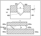
- Non-Patent Document 2 A technique called Aspect Ratio Trapping (ART) is known as a method for achieving this (Non-Patent Document 2). As shown in Figure 6, this technique uses Si layers 401, 401a, first selective growth masks 402, 402a, and second selective growth masks 403, 403a. Grooves 404, 404a are formed by the first selective growth masks 402, 402a and the second selective growth masks 403, 403a.
- the groove depth h of the grooves 404, 404a is made larger than the groove width w of the grooves 404, 404a, and the III-V compound semiconductor layers 405, 405a are epitaxially grown from the Si layers 401, 401a. During this growth, the growth of defects 406 that occur at the interface between the Si layers 401, 401a and the III-V compound semiconductor layers 405, 405a is stopped (terminated) at the side walls of the grooves 404, 404a, and high-quality III-V compound semiconductor crystals are grown above the defect regions.
- a waveguide-type photodiode disclosed in Non-Patent Document 3 is an example of a thin-film optical device that has been produced using this technology.
- Non-Patent Document 3 uses a Si layer as a seed crystal and epitaxial growth technology in the horizontal direction of the substrate to form the III-V compound semiconductor layer. Therefore, with this technology, the III-V compound semiconductor layer and active layer exist on the same plane as the Si waveguide formed using the same Si layer. This creates the problem that it is difficult to integrate the Si waveguide and the III-V compound semiconductor layer at different positions in the thickness direction, as shown in Non-Patent Document 1.
- the present invention was made to solve the above problems, and aims to make it easier to manufacture semiconductor lasers that integrate a Si waveguide and a III-V compound semiconductor layer at different positions in the thickness direction.
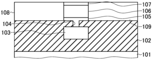
- the semiconductor laser according to the present invention comprises an optical waveguide made of a Si core formed on a substrate and a cladding layer in which the Si core is embedded; a groove formed in the cladding layer above the Si core, extending along the Si core and reaching the Si core; a lower semiconductor layer made of compound semiconductors that is epitaxially grown from the top surface of the Si core at the bottom of the groove to fill the groove and is formed on the cladding layer, and extends along the Si core; an active layer made of compound semiconductors formed on the lower semiconductor layer, extending along the Si core in a state capable of optically coupling with the Si core; an upper semiconductor layer made of compound semiconductors and formed on the active layer; a p-type semiconductor layer and an n-type semiconductor layer made of compound semiconductors formed on the cladding layer and in contact with the active layer; an n-type electrode connected to the n-type semiconductor layer; a p-type electrode connected to the p-type semiconductor layer; and a resonator structure that confines light in the
- a lower semiconductor layer is formed on the cladding layer by epitaxial growth from the top surface of the Si core at the bottom surface of the groove formed in the cladding layer above the Si core, and an active layer is then formed on top of this.
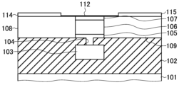
- FIG. 2H is a cross-sectional view showing a state of a semiconductor laser in the middle of a process for explaining a method for manufacturing a semiconductor laser according to an embodiment of the present invention.
- FIG. 3 is a characteristic diagram showing the dependence of the optical confinement factor of the active layer 106, Si core 103, and groove 104 on the width of the groove 104 from 0 to 100 nm when the width of the Si core 103 is 440 nm.
- FIG. 4 is a characteristic diagram showing the dependence of the optical confinement factor of the active layer 106, Si core 103, and groove 104 on the width of the groove 104 from 0 to 100 nm when the width of the Si core 103 is 700 nm.
- FIG. 3 is a characteristic diagram showing the dependence of the optical confinement factor of the active layer 106, Si core 103, and groove 104 on the width of the groove 104 from 0 to 100 nm when the width of the Si core 103 is 700 nm.
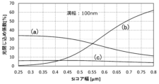
- FIG. 5 is a characteristic diagram showing the dependence of the optical confinement factor of each layer when the width of the Si core 103 is changed from 250 nm to 800 nm while the width of the groove 104 is fixed at 100 nm.
- FIG. 6 is an explanatory diagram for explaining aspect ratio trapping.
- the semiconductor laser also includes a groove 104 formed in the cladding layer 102.
- the groove 104 is disposed on the Si core 103 and is formed to extend along the Si core 103.
- the groove 104 is also formed to reach the Si core 103 in the thickness direction.
- the bottom surface of the groove 104 becomes the upper surface of the Si core 103.
- the groove 104 is formed so that the depth of the groove 104 is greater than the width of the groove 104.
- the lower semiconductor layer 105 is formed on the cladding layer 102 by epitaxial growth from the top surface of the Si core 103 at the bottom of the groove 104, filling the groove 104.
- the lower semiconductor layer 105 is formed by epitaxial growth without defects above the cladding layer 102, by stopping the growth of defects generated from the top surface of the Si core 103 at the bottom of the groove 104 at the side of the groove 104 using aspect ratio trapping (ART) using the groove 104.
- the lower semiconductor layer 105 is also formed extending along the Si core 103.
- the lower semiconductor layer 105 can be composed of, for example, undoped InP.
- the lower semiconductor layer 105 can be formed directly above the Si core 103.
- the active layer 106 is formed on the lower semiconductor layer 105 in a state capable of optically coupling with the Si core 103.
- the active layer 106 is formed to extend along the Si core 103 together with the lower semiconductor layer 105.
- the active layer 106 can have a multiple quantum well structure in which well layers and barrier layers made of InGaAsP are alternately stacked.
- the active layer 106 can have a multiple quantum well structure in which well layers made of InGaAs and barrier layers made of InP are alternately stacked.
- the upper semiconductor layer 107 is formed on the active layer 106.
- the upper semiconductor layer 107 is formed to extend along the Si core 103 together with the active layer 106.
- the upper semiconductor layer 107 can be made of, for example, undoped InP (i-InP).
- the lower semiconductor layer 105 and the upper semiconductor layer 107 can be clad to confine light to the active layer 106.
- a diffraction grating 112 is formed as a resonator structure that confines light to the active layer 106.
- the diffraction grating 112 is composed of, for example, a grating pattern formed on the top surface of the upper semiconductor layer 107.
- This semiconductor laser also includes a p-type semiconductor layer 108 and an n-type semiconductor layer 109 formed on the cladding layer 102 and in contact with the active layer 106.
- the p-type semiconductor layer 108 and the n-type semiconductor layer 109 are formed to sandwich the lower semiconductor layer 105, the active layer 106, and the upper semiconductor layer 107 in a plan view. With this configuration, a current is injected into the active layer 106 in a direction parallel to the plane of the substrate 101.
- the p-type semiconductor layer 108 can be made of p-type InP doped with Zn at about 1 ⁇ 10 18 cm ⁇ 3 , for example.
- the n-type semiconductor layer 109 can be made of n-type InP doped with Si at about 1 ⁇ 10 18 cm ⁇ 3 , for example.
- the semiconductor laser also includes a p-type electrode 110 electrically connected to the p-type semiconductor layer 108, and an n-type electrode 111 electrically connected to the n-type semiconductor layer 109.
- the semiconductor laser also includes a first contact layer 114 formed on the p-type semiconductor layer 108, and a second contact layer 115 formed on the n-type semiconductor layer 109.
- the p-type electrode 110 is formed on the first contact layer 114 in ohmic contact, and the n-type electrode 111 is formed on the second contact layer 115 in ohmic contact.
- the first contact layer 114 may be made of p-type InP doped with Zn at about 1 ⁇ 10 19 cm -3 .
- the second contact layer 115 may be made of n-type InP doped with Si at about 1 ⁇ 10 19 cm -3 .
- an insulating layer 113 is formed on and in contact with the upper semiconductor layer 107, the p-type semiconductor layer 108, and the n-type semiconductor layer 109 between the first contact layer 114 and the second contact layer 115.
- the lower semiconductor layer 105 is formed by epitaxially growing from the top surface of the Si core 103 at the bottom of the groove 104 using the Si core 103 as a seed crystal to fill the groove 104.
- This allows defects (dislocations) that occur at the interface between the lower semiconductor layer 105 and the Si core 103 to be terminated on the inner wall of the groove 104, and the lower semiconductor layer 105 above the cladding layer 102 can be made into a good quality crystal.
- the width w of the groove 104 is set to 100 (nm) and the height h of the groove 104 is set to 150 (nm)
- a good quality III-V compound semiconductor can be grown on the cladding layer 102.
- This means that a good quality active layer 106 can be formed at a distance that allows optical coupling with the Si core 103.
- the groove 104 can have a groove width of 0.1 ⁇ m or less. By making the groove width of the groove 104 0.1 ⁇ m or less, it is possible to suppress leakage of light from the Si core 103 to the lower semiconductor layer 105 side.
- an optical waveguide is formed on a substrate 101, which is made up of a Si core 103 and a cladding layer 102 in which the Si core 103 is embedded (first step).
- a groove 104 is formed in the cladding layer 102 on the Si core 103, extending along the Si core 103 and reaching the Si core 103 (second step).
- the groove 104 can be formed by selectively etching away the cladding layer 102 using a dry etching process that uses a mask pattern formed by known lithography technology.
- the groove 104 is formed so that the depth of the groove 104 is greater than the width of the groove 104.
- the groove 104 is formed so that the width of the groove 104 is 0.1 ⁇ m or less.
- a lower semiconductor layer 105 is formed on the cladding layer 102, filling the grooves 104 and extending along the Si core 103 (third step).
- the lower semiconductor layer 105 is formed by epitaxial growth from the top surface of the Si core 103 at the bottom of the grooves 104.
- the lower semiconductor layer 105 is formed by epitaxially growing undoped InP using the well-known metalorganic vapor phase epitaxy method.
- the lower semiconductor layer 105 is formed by epitaxial growth without defects above the cladding layer 102, by stopping the growth of defects that arise from the top surface of the Si core 103 at the bottom of the groove 104 at the side of the groove 104 during the growth of the III-V compound semiconductor (e.g., InP) using aspect ratio trapping with the groove 104.
- the III-V compound semiconductor e.g., InP
- the growth in the direction parallel to the plane of the substrate 101 is appropriately controlled, and the width of the lower semiconductor layer 105 in the width direction of the groove 104 is formed to a set value.
- an active layer 106 made of a III-V compound semiconductor is formed on the lower semiconductor layer 105, extending along the Si core 103 in a state capable of optically coupling with the Si core 103 (fourth step).
- the III-V compound semiconductor that will become the active layer 106 is epitaxially grown from the upper surface of the lower semiconductor layer 105 to form the active layer 106.
- the sides of the lower semiconductor layer 105 are the upper surfaces of the cladding layer 102 made of a dielectric material such as silicon oxide, and by appropriately setting the growth conditions for the III-V compound semiconductor, the active layer 106 can be selectively grown only on the lower semiconductor layer 105.
- an upper semiconductor layer 107 made of a III-V compound semiconductor is formed on the active layer 106 (step 5).
- the lower semiconductor layer 105 and the upper semiconductor layer 107 are formed by epitaxially growing undoped InP using the well-known metalorganic vapor phase epitaxy method.
- the side of the lower semiconductor layer 105 is the upper surface of the cladding layer 102 made of a dielectric material such as silicon oxide, and by appropriately setting the growth conditions for the III-V compound semiconductor, the upper semiconductor layer 107 can be selectively grown only on the active layer 106.
- a p-type semiconductor layer 108 and an n-type semiconductor layer 109 made of compound semiconductors are formed on the cladding layer 102 in contact with the active layer 106 (step 6).
- the p-type semiconductor layer 108 and the n-type semiconductor layer 109 are formed sandwiching the lower semiconductor layer 105, the active layer 106, and the upper semiconductor layer 107 in a plan view.
- a III-V compound semiconductor e.g., undoped InP
- a III-V compound semiconductor is grown (regrown) from the side of the lower semiconductor layer 105 (upper semiconductor layer 107) in a direction parallel to the plane of the substrate 101 (References 1 and 2).
- Both sides of the stacked structure of the lower semiconductor layer 105, active layer 106, and upper semiconductor layer 107 are filled with the grown compound semiconductor layer.
- the compound semiconductor layer on one side of the stacked structure of the lower semiconductor layer 105, active layer 106, and upper semiconductor layer 107 is doped with a p-type impurity to form a p-type semiconductor layer 108.
- the compound semiconductor layer on the other side of the stacked structure of the lower semiconductor layer 105, active layer 106, and upper semiconductor layer 107 is doped with an n-type impurity to form an n-type semiconductor layer 109.
- a diffraction grating 112 is formed above the active layer 106 as a resonator structure (step 8).
- a configuration can be adopted in which the first contact layer 114 is formed on the p-type semiconductor layer 108, and the second contact layer 115 is formed on the n-type semiconductor layer 109 (step 9).
- a grown compound semiconductor layer e.g., undoped InP
- a compound semiconductor layer e.g., undoped InGaAs
- a compound semiconductor layer e.g., undoped InGaAs
- the compound semiconductor layer on one side of the stacked structure of the lower semiconductor layer 105, the active layer 106, and the upper semiconductor layer 107 is doped with p-type impurities to form the p-type semiconductor layer 108 and the first contact layer 114.
- the compound semiconductor layer on the other side of the stacked structure of the lower semiconductor layer 105, the active layer 106, and the upper semiconductor layer 107 is doped with an n-type impurity to form an n-type semiconductor layer 109 and a second contact layer 115.
- a p-type electrode 110 electrically connected to the p-type semiconductor layer 108 is formed on the first contact layer 114, and an n-type electrode 111 electrically connected to the n-type semiconductor layer 109 is formed on the second contact layer 115 (seventh step). Furthermore, an insulating layer 113 is formed on the upper semiconductor layer 107, the p-type semiconductor layer 108, and the n-type semiconductor layer 109 between the first contact layer 114 and the second contact layer 115.
- the core structure of the active layer 106 can be formed without patterning using photolithography and etching techniques, simplifying the manufacturing process.
- the III-V compound semiconductor filling the grooves 104 is in contact with the upper surface of part of the Si core 103, so it is expected that the light confinement in the active layer 106 and the Si core 103 will be affected.
- the results of an investigation into this effect are shown below.
- Figure 3 shows the dependence of the optical confinement coefficient of the active layer 106, Si core 103, and groove 104 on the width of the groove 104 from 0 to 100 nm when the width of the Si core 103 is 440 nm.
- Figure 4 shows the dependence of the optical confinement coefficient of the active layer 106, Si core 103, and groove 104 on the width of the groove 104 from 0 to 100 nm when the width of the Si core 103 is 700 nm.
- (a) shows the dependence of the optical confinement coefficient of the active layer 106
- (b) shows the dependence of the optical confinement coefficient of the Si core 103
- (c) shows the dependence of the optical confinement coefficient of the groove 104.
- the active layer 106 has a multiple quantum well structure with a thickness of 100 nm, a width of 500 nm, and a refractive index of 3.5.
- the lower semiconductor layer 105 and the upper semiconductor layer 107 are made of InP with a refractive index of 3.16, and the Si core 103 was calculated to have a refractive index of 3.478.
- the calculation results when the groove 104 width is 0 nm correspond to the optical confinement coefficient of each layer in the conventional structure in which the groove 104 does not exist.
Landscapes
- Physics & Mathematics (AREA)
- Condensed Matter Physics & Semiconductors (AREA)
- General Physics & Mathematics (AREA)
- Electromagnetism (AREA)
- Optics & Photonics (AREA)
- Semiconductor Lasers (AREA)
Priority Applications (2)
| Application Number | Priority Date | Filing Date | Title |
|---|---|---|---|
| PCT/JP2023/027570 WO2025022643A1 (ja) | 2023-07-27 | 2023-07-27 | 半導体レーザおよびその製造方法 |
| JP2025535527A JPWO2025022643A1 (https=) | 2023-07-27 | 2023-07-27 |
Applications Claiming Priority (1)
| Application Number | Priority Date | Filing Date | Title |
|---|---|---|---|
| PCT/JP2023/027570 WO2025022643A1 (ja) | 2023-07-27 | 2023-07-27 | 半導体レーザおよびその製造方法 |
Publications (1)
| Publication Number | Publication Date |
|---|---|
| WO2025022643A1 true WO2025022643A1 (ja) | 2025-01-30 |
Family
ID=94374178
Family Applications (1)
| Application Number | Title | Priority Date | Filing Date |
|---|---|---|---|
| PCT/JP2023/027570 Pending WO2025022643A1 (ja) | 2023-07-27 | 2023-07-27 | 半導体レーザおよびその製造方法 |
Country Status (2)
| Country | Link |
|---|---|
| JP (1) | JPWO2025022643A1 (https=) |
| WO (1) | WO2025022643A1 (https=) |
Citations (4)
| Publication number | Priority date | Publication date | Assignee | Title |
|---|---|---|---|---|
| JPS62213117A (ja) * | 1986-03-13 | 1987-09-19 | Oki Electric Ind Co Ltd | 半導体素子の製造方法 |
| JPH05206565A (ja) * | 1991-06-12 | 1993-08-13 | Oki Electric Ind Co Ltd | 半導体レーザ素子 |
| WO2021005700A1 (ja) * | 2019-07-09 | 2021-01-14 | 日本電信電話株式会社 | 半導体光素子 |
| US20210273409A1 (en) * | 2020-02-27 | 2021-09-02 | Qualcomm Incorporated | Distributed feedback (dfb) laser on silicon and integrated device comprising a dfb laser on silicon |
-
2023
- 2023-07-27 JP JP2025535527A patent/JPWO2025022643A1/ja active Pending
- 2023-07-27 WO PCT/JP2023/027570 patent/WO2025022643A1/ja active Pending
Patent Citations (4)
| Publication number | Priority date | Publication date | Assignee | Title |
|---|---|---|---|---|
| JPS62213117A (ja) * | 1986-03-13 | 1987-09-19 | Oki Electric Ind Co Ltd | 半導体素子の製造方法 |
| JPH05206565A (ja) * | 1991-06-12 | 1993-08-13 | Oki Electric Ind Co Ltd | 半導体レーザ素子 |
| WO2021005700A1 (ja) * | 2019-07-09 | 2021-01-14 | 日本電信電話株式会社 | 半導体光素子 |
| US20210273409A1 (en) * | 2020-02-27 | 2021-09-02 | Qualcomm Incorporated | Distributed feedback (dfb) laser on silicon and integrated device comprising a dfb laser on silicon |
Non-Patent Citations (2)
| Title |
|---|
| LI, ZHIBO ET AL.: "Monolithic integration of InGaAs/InP multiple quantum wells on SOI substrates for photonic devices", JOURNAL OF APPLIED PHYSICS, vol. 123, February 2018 (2018-02-01), pages 1 - 6, XP012226151, DOI: 10.1063/1.5009639 * |
| TRAN, M.A. ET AL.: "Tutorial on narrow linewidth tunable semiconductor lasers using Si/III-V heterogeneous integration", APL PHOTONICS, vol. 4, November 2019 (2019-11-01), pages 1 - 19, XP012241940, DOI: 10.1063/1.5124254 * |
Also Published As
| Publication number | Publication date |
|---|---|
| JPWO2025022643A1 (https=) | 2025-01-30 |
Similar Documents
| Publication | Publication Date | Title |
|---|---|---|
| JP5897414B2 (ja) | 光デバイスの製造方法 | |
| JP3285426B2 (ja) | 半導体光集積素子及びその製造方法 | |
| JPS6215875A (ja) | 半導体装置およびその製造方法 | |
| JP2004179274A (ja) | 光半導体装置 | |
| JP2010263153A (ja) | 半導体集積光デバイス及びその作製方法 | |
| JP2746326B2 (ja) | 半導体光素子 | |
| JP6839035B2 (ja) | 半導体装置の製造方法 | |
| CN103762497A (zh) | 基于重构-等效啁啾和等效半边切趾的dfb半导体激光器及制备方法 | |
| CN118825769A (zh) | 侧向非晶硅光子晶体激光器、激光器阵列及制备方法 | |
| US20230318263A1 (en) | Optoelectronic device comprising a iii-v semiconductor membrane laser source forming a lateral p-i-n junction | |
| JPH04397B2 (https=) | ||
| KR0174303B1 (ko) | 반도체장치 및 그 제조방법 | |
| US6853661B2 (en) | Gain-coupled semiconductor laser device lowering blue shift | |
| JP4097950B2 (ja) | 分布帰還型レーザ装置、半導体光装置および分布帰還型レーザ装置の製造方法 | |
| WO2025022643A1 (ja) | 半導体レーザおよびその製造方法 | |
| JPH05110187A (ja) | アレイ型半導体レーザ及びその製造方法 | |
| JPH08274295A (ja) | 光半導体装置の製造方法 | |
| JP3242958B2 (ja) | 光半導体素子 | |
| JP4192324B2 (ja) | 半導体レーザ素子およびその製造方法 | |
| WO2025022644A1 (ja) | 半導体レーザ | |
| JP2947227B2 (ja) | 半導体光増幅器、その製造方法及び利得の偏光依存性の補償方法 | |
| JP7750408B2 (ja) | 半導体受光器および半導体素子 | |
| Matsuo | High-performance lasers on InP-SOI platform | |
| WO2026074602A1 (ja) | 半導体光デバイス | |
| JPH08330665A (ja) | 光半導体レーザの製造方法 |
Legal Events
| Date | Code | Title | Description |
|---|---|---|---|
| 121 | Ep: the epo has been informed by wipo that ep was designated in this application |
Ref document number: 23946723 Country of ref document: EP Kind code of ref document: A1 |
|
| ENP | Entry into the national phase |
Ref document number: 2025535527 Country of ref document: JP Kind code of ref document: A |
|
| WWE | Wipo information: entry into national phase |
Ref document number: 2025535527 Country of ref document: JP |
|
| NENP | Non-entry into the national phase |
Ref country code: DE |