WO2025017870A1 - 電力変換装置及び空気調和装置 - Google Patents
電力変換装置及び空気調和装置 Download PDFInfo
- Publication number
- WO2025017870A1 WO2025017870A1 PCT/JP2023/026425 JP2023026425W WO2025017870A1 WO 2025017870 A1 WO2025017870 A1 WO 2025017870A1 JP 2023026425 W JP2023026425 W JP 2023026425W WO 2025017870 A1 WO2025017870 A1 WO 2025017870A1
- Authority
- WO
- WIPO (PCT)
- Prior art keywords
- phase
- switching
- period
- voltage
- inverter
- Prior art date
- Legal status (The legal status is an assumption and is not a legal conclusion. Google has not performed a legal analysis and makes no representation as to the accuracy of the status listed.)
- Pending
Links
Images




Classifications
-
- H—ELECTRICITY
- H02—GENERATION; CONVERSION OR DISTRIBUTION OF ELECTRIC POWER
- H02M—APPARATUS FOR CONVERSION BETWEEN AC AND AC, BETWEEN AC AND DC, OR BETWEEN DC AND DC, AND FOR USE WITH MAINS OR SIMILAR POWER SUPPLY SYSTEMS; CONVERSION OF DC OR AC INPUT POWER INTO SURGE OUTPUT POWER; CONTROL OR REGULATION THEREOF
- H02M7/00—Conversion of AC power input into DC power output; Conversion of DC power input into AC power output
- H02M7/42—Conversion of DC power input into AC power output without possibility of reversal
- H02M7/44—Conversion of DC power input into AC power output without possibility of reversal by static converters
- H02M7/48—Conversion of DC power input into AC power output without possibility of reversal by static converters using discharge tubes with control electrode or semiconductor devices with control electrode
Definitions
- This disclosure relates to a power conversion device and an air conditioning device equipped with an inverter that converts DC power into AC power and supplies it to a three-phase load.
- Pulse Width Modulation (PWM) drive is generally used as the drive method for each switching element provided in the inverter.
- Common modulation methods for sine wave modulation using PWM include “three-phase modulation” and “two-phase modulation.” When using three-phase modulation and two-phase modulation together, three-phase modulation is generally used, and when it is desired to reduce switching losses, it is common to switch from three-phase modulation to two-phase modulation.
- An inverter has legs consisting of upper and lower elements (hereinafter referred to as "upper and lower elements") connected in series.
- the drive signal for driving the upper and lower elements of the inverter has a period called dead time during which the upper and lower elements are simultaneously turned off to prevent a leg short circuit caused by the upper and lower elements being turned on at the same time.
- the dead time corresponds to a disturbance voltage. For this reason, for example, if the three-phase load is a motor, the dead time can cause ripples in the motor current and motor torque, which can have an adverse effect on noise and vibration.
- non-patent document 1 discloses a technique for reducing ripples in the motor current and motor torque by superimposing a correction voltage on the voltage command for each phase based on the DC bus voltage, motor current, and carrier frequency used to generate the drive signal. This correction is called dead-time correction.
- Patent Document 1 discloses a control method for an inverter circuit in a three-phase voltage-type inverter that obtains three-phase AC voltage from a DC power source, in which a bottom-attached two-phase modulation method or a top-attached two-phase modulation method that reduces the maximum value of leakage current in the low-speed range according to the rotation speed, and a top-attached two-phase modulation method that ensures speed stability in the high-speed range are selected.
- the bottom-attached two-phase modulation method is a modulation method in which the voltage amplitude command for each phase is set to the minimum value every 120 degrees, which is 1/3 of one electrical angle cycle, and the bottom element of the top and bottom elements of the inverter is maintained in the on state for a period of 120 degrees.
- the top-attached two-phase modulation method is a modulation method in which the positive and negative of the bottom-attached two-phase modulation method is reversed, that is, a modulation method in which the top element of the top and bottom elements of the inverter is maintained in the on state for a period of 120 degrees.
- the top-and-bottom-attached two-phase modulation method is a method in which both bottom-attached two-phase modulation and top-attached two-phase modulation are alternately performed every 60 degrees within one electrical angle cycle.
- the present disclosure has been made in consideration of the above, and aims to obtain a power conversion device that can sufficiently suppress ripples in the motor current and motor torque even when a drive method that combines three-phase modulation and two-phase modulation is adopted.
- the power conversion device includes an inverter that converts DC power into AC power and supplies it to a three-phase load, and a control unit that generates switching signals for a plurality of three-phase switching elements provided in the inverter and outputs the switching signals to the inverter.
- the control unit performs two-phase modulation that sequentially suspends the switching operation of the switching elements of one of the three phases, and inserts a three-phase modulation period in which all three phases are subjected to switching operation at least one of immediately before and after the timing at which the phase in which the switching operation is suspended transitions from a switching period to a switching suspend period based on the current flowing in and out of the inverter when performing the two-phase modulation, and at least one of immediately before and after the timing at which the phase in which the switching operation is suspended transitions from a switching suspend period to a switching period.
- the power conversion device disclosed herein has the advantage that ripples in the motor current and motor torque can be sufficiently suppressed even when a drive method that combines three-phase modulation and two-phase modulation is adopted.
- FIG. 1 is a diagram for explaining a basic configuration and basic functions of a power conversion device according to a first embodiment.
- FIG. 2 is a diagram showing another example of a configuration having the basic functions of the power conversion device shown in FIG. 1;
- FIG. 2 is a diagram showing yet another example of a configuration having the basic functions of the power conversion device shown in FIG.
- FIG. 1 is a block diagram for explaining a basic function related to generation of a switching signal in a control unit according to a first embodiment;
- FIG. 1 is a diagram for explaining problems in the prior art.
- FIG. 10 is a diagram for explaining a second three-phase voltage modulated wave generated inside the control unit according to the first embodiment;
- FIG. 1 is a diagram showing an example of a characteristic table referenced within a control unit according to the first embodiment
- FIG. 13 is a diagram showing a relationship between a u-phase Td correction value generated inside the control unit according to the first embodiment and a u-phase current.
- FIG. 1 is a diagram for explaining the relationship between first, second, and third three-phase voltage modulated waves generated inside a control unit according to the first embodiment;
- FIG. 1 is a diagram for explaining a method for setting a shift amount in the first embodiment;
- FIG. 10 is a diagram for explaining another method for setting the shift amount in the first embodiment;
- FIG. 12 is a block diagram of a control unit that realizes the modulation method selection control described with reference to FIG. 10 and FIG. 11.
- FIG. 11 is a block diagram of a control unit that realizes the modulation method selection control described with reference to FIG. 10 and FIG. 11.
- FIG. 1 is a diagram showing an example of waveforms of a phase current and a q-axis current in a conventional two-phase modulation
- FIG. 1 is a diagram showing an example of waveforms of a phase current and a q-axis current when the power conversion device according to the first embodiment is used
- FIG. 1 is a first diagram for explaining a three-phase modulation insertion period inserted by control according to a second embodiment
- FIG. 2 is a second diagram illustrating a three-phase modulation insertion period inserted by the control according to the second embodiment
- FIG. 1 is a first diagram for explaining a three-phase modulation insertion period inserted by control according to a third embodiment
- FIG. 2 is a second diagram illustrating a three-phase modulation insertion period inserted by the control according to the third embodiment
- FIG. 13 is a diagram for explaining a three-phase modulation insertion period inserted by control according to the fourth embodiment
- FIG. 13 is a diagram showing a configuration example of an air conditioning device according to a sixth embodiment.
- FIG. 13 is a diagram showing an example of a hardware configuration for implementing the functions of a control unit in the first to fifth embodiments.
- FIG. 13 is a diagram showing another example of a hardware configuration for implementing the functions of the control unit in the first to fifth embodiments.
- Fig. 1 is a diagram for explaining a basic configuration and basic functions of a power conversion device 100 according to a first embodiment.
- the power conversion device 100 is connected between a commercial power source 1 and a motor 5.
- the commercial power source 1 is an example of an AC power source.
- the motor 5 is a three-phase motor mounted on a three-phase load.
- a compressor that compresses a refrigerant, a fan that blows air to a heat exchanger that exchanges heat with the refrigerant, and the like correspond to the three-phase load.
- the power conversion device 100 includes a converter 2, an inverter 3, and a control unit 4.
- the converter 2 rectifies the power supply voltage applied from the commercial power supply 1 and outputs it to the inverter 3. If the converter 2 has a boost function, the converter 2 outputs a boosted voltage obtained by boosting the power supply voltage to the inverter 3. In other words, the converter 2 rectifies the power supply voltage applied from the commercial power supply 1, and also performs the operation of boosting the power supply voltage if necessary.
- the inverter 3 is connected to the output terminal of the converter 2 by electrical wiring 6a and 6b.
- the electrical wiring 6a and 6b are also called DC busbars.
- the electrical wiring 6a is a DC busbar on the high potential side
- the electrical wiring 6b is a DC busbar on the low potential side.
- the inverter 3 has switching elements 31a, 31b, 31c, 32a, 32b, and 32c with freewheel diodes connected in inverse parallel.
- the switching elements 31a to 31c are the upper elements described above, and the switching elements 32a to 32c are the lower elements described above.
- the switching elements 31a to 31c and 32a to 32c are turned on or off under the control of the control unit 4, and the inverter 3 converts the DC power output from the converter 2 into AC power having the desired amplitude and phase and supplies it to the motor 5. Note that FIG.
- switching elements 31a to 31c and 32a to 32c are IGBTs (Insulated Gate Bipolar Transistors), but MOSFETs (Metal Oxide Semiconductor Field Effect Transistors) may be used instead of IGBTs.
- MOSFETs Metal Oxide Semiconductor Field Effect Transistors
- parasitic diodes are built in, so in some cases a configuration is used in which the diodes are not connected in inverse parallel.
- the inverter 3 also has shunt resistors 33a, 33b, and 33c for detecting the current flowing through each phase of the inverter 3.
- the shunt resistor 33a is connected between the switching element 32a, which is the lower element, and the low-potential side electrical wiring 6b.
- the shunt resistors 33b and 33c are connected in a similar manner.
- the detection values of the shunt resistors 33a to 33c are input to the control unit 4.
- the control unit 4 calculates the voltage detected by the shunt resistors 33a to 33c and converts it into a current to obtain the current flowing through each phase of the inverter 3. Once the current flowing through each phase of the inverter 3 has been obtained, the three-phase output current output from the inverter 3 to the motor 5 can also be obtained.
- the control unit 4 also receives the detected value of the bus voltage Vdc from the converter 2.
- the bus voltage Vdc is the voltage between the electrical wiring 6a and 6b, which are DC buses.
- the bus voltage Vdc may be the voltage across a smoothing capacitor (not shown in FIG. 1) that smoothes the output voltage of the converter 2.
- the control unit 4 generates switching signals for the three-phase switching elements 31a-31c, 32a-32c provided in the inverter 3 based on the current flowing through each phase of the inverter 3 and the bus voltage Vdc, and outputs the signals to the inverter 3.
- the on and off operations of the switching elements 31a-31c, 32a-32c are controlled by the switching signals.
- FIG. 2 is a diagram showing another example configuration having the basic functions of the power conversion device 100 shown in FIG. 1.
- FIG. 1 shows a configuration known as a three-shunt system
- FIG. 2 shows a configuration known as a one-shunt system.
- the current flowing through each phase of inverter 3 is detected based on the timing at which switching elements 31a-31c, 32a-32c are turned on or off.
- the method of detecting the current flowing through each phase of inverter 3 based on the detection value of shunt resistor 34 is well known, and further explanation will be omitted here.
- FIG. 3 is a diagram showing yet another example configuration having the basic functions of the power conversion device 100 shown in FIG. 1.
- the shunt resistors 33a to 33c have been removed, and current detectors 35a and 35b have been inserted into the electrical wiring 7 connecting the inverter 3 and the motor 5.
- Each of the current detectors 35a and 35b detects the current of one phase of the three-phase output current that is the output current of the inverter 3.
- the detection values of the current detectors 35a and 35b are input to the control unit 4.
- the control unit 4 calculates the current of the remaining one phase based on the detection values of the currents of any two phases detected by the current detectors 35a and 35b.
- Typical current detectors 35a and 35b include an ACCT (Alternating Current Transformer) that can detect only AC components, and a DCCT (Direct Current Transformer) that can detect both DC and AC components, but any detector that can detect three-phase output current may be used.
- ACCT Alternating Current Transformer
- DCCT Direct Current Transformer
- FIG. 4 is a block diagram for explaining the basic functions related to generation of a switching signal in the control unit 4 according to the first embodiment.
- the control unit 4 according to the first embodiment generates a switching signal by using three-phase modulation and two-phase modulation in combination, and for implementing this control, the control unit 4 has an internal functional block as shown in FIG. 4.
- the control unit 4 includes a modulation method selection unit 41, a modulated wave generation unit 42, a Td correction unit 43, a PWM modulation unit 44, and a Td addition unit 45. Note that "Td" in the Td correction unit 43 and the Td addition unit 45 means dead time.
- the modulated wave generating unit 42 When a positive modulation factor command Vk and a voltage phase ⁇ are given, the modulated wave generating unit 42 generates first three-phase voltage modulated waves Vu1 * , Vv1 * , Vw1 * as shown in the following equation (1).
- Vw1 * Vk ⁇ cos( ⁇ -4/3 ⁇ ) ...(1)
- the first three-phase voltage modulated waves Vu1 * , Vv1 * , Vw1 * essentially correspond to the desired voltages to be output from the inverter 3, and are generated based on voltage commands output from a higher-level control system (not shown).
- the voltage phase ⁇ is the phase of the three-phase output voltage, which is the output voltage of the inverter 3, and is the phase when the rotation of the motor 5 is viewed in terms of electrical angle.
- the modulation method selection unit 41 selects and instructs a modulation method based on the modulation factor command Vk and the voltage phase ⁇ .
- the modulation wave generation unit 42 outputs the first three-phase voltage modulation waves Vu1 * , Vv1 * , Vw1 * as the second three-phase voltage modulation waves Vu2 * , Vv2 * , Vw2 * .
- the modulation wave generation unit 42 generates the second three-phase voltage modulation waves Vu2 * , Vv2 * , Vw2 * shown in the following formula (2) and outputs them to the Td correction unit 43.
- Vu2 * Vu1 * -Vcom
- Vv2 * Vv1 * -Vcom
- Vw2 * Vw1 * -Vcom ...(2)
- Vcom is a three-phase common signal.
- the second three-phase voltage modulation waves Vu2 * , Vv2 * , Vw2 * are generated by subtracting the same value of the three-phase common signal Vcom from the first three-phase voltage modulation waves Vu1 * , Vv1 * , Vw1 *, so that the line voltage value between each phase is maintained.
- the three-phase common signal Vcom can be calculated, for example, by the following formula (3).
- Vcom min(Vu1 * ,Vv1 * ,Vw1 * )+1...(3)
- min(Vu1 * , Vv1 * , Vw1 * ) is a function for obtaining the minimum value among the first three-phase voltage modulated waves Vu1 * , Vv1 * , Vw1 * .
- the Td correction unit 43 generates third three-phase voltage modulated waves Vu3 * , Vv3 * , Vw3 * by correcting the second three-phase voltage modulated waves Vu2*, Vv2*, Vw2* based on the three-phase output currents iu , iv, iw , the bus voltage Vdc, and the carrier frequency fc .
- the Td correction unit 43 is implemented with a current characteristic when the dead time Td is regarded as a disturbance voltage.
- the Td correction unit 43 corrects the second three-phase voltage modulated waves Vu2 * , Vv2 * , Vw2 * by referring to the current characteristic according to the values of the three-phase output currents iu, iv, iw.
- the PWM modulation unit 44 internally generates a carrier signal of the commanded carrier frequency fc, compares the third three-phase voltage modulation waves Vu3*, Vv3 * , Vw3 * with the carrier signal, and generates a switching signal SW1 based on the magnitude relationship between the carrier signal and the third three-phase voltage modulation waves Vu3 * , Vv3*, Vw3*.
- This switching signal SW1 is a signal before the dead time Td is added.
- the Td addition unit 45 generates a switching signal SW by adding the dead time Td to the switching signal SW1, and outputs the switching signal SW to the inverter 3.
- Figure 5 is a diagram for explaining the problems of the conventional technology.
- the operating waveforms in Figure 5 are those during two-phase modulation, and the solid line, dashed line, and thick dashed line represent the u-phase voltage modulated wave Vu2 * , the v-phase voltage modulated wave Vv2 *, and the w-phase voltage modulated wave Vw2 *, respectively.
- the thick solid line represents the u-phase current iu of the three-phase output currents iu, iv, and iw.
- the horizontal axis represents the electrical angle phase angle
- the vertical axis represents the voltage value of each modulated wave or the current value of the u-phase current iu.
- the voltage value on the vertical axis is normalized to ⁇ 1, and the value on the vertical axis corresponds to the modulation factor.
- Period Xa is the three-phase modulation period immediately before the u-phase switching pause period Yu during which two-phase modulation is performed.
- Period Xb is the three-phase modulation period immediately after the u-phase switching pause period Yu during which two-phase modulation is performed.
- the minimum pulse width is set to protect the switching elements 31a to 31c, 32a to 32c and to ensure the current detection function.
- the portion surrounded by the u-phase voltage modulated wave Vu2 * and the rectangular frames in the periods Xa and Xb is hatched.
- the size of the area of the hatched portion represents the voltage manipulation margin for Td correction.
- the larger the area of the hatched portion the larger the voltage manipulation margin.
- the voltage manipulation margin can be increased by expanding the periods Xa and Xb, such a method does not solve the problem. This is because, as the u-phase switching pause period Yu approaches, the difference between the u-phase voltage modulated wave Vu2 * and the first limiter value Limit1 becomes smaller, and the voltage manipulation margin becomes rapidly smaller, making it difficult to perform Td correction sufficiently.
- the period immediately before and after the u-phase switching pause period Yu is a period in which there is a voltage control error that makes it impossible to perform Td correction sufficiently.
- there is no switching operation during the u-phase switching pause period Yu and therefore no voltage control error exists. Therefore, at the timing when the period Xa switches to the u-phase switching pause period Yu, and when the u-phase switching pause period Yu switches to the period Xb, the voltage control error changes in a step-like manner, causing current ripples and torque ripples.
- a method for calculating the second three-phase voltage modulated waves Vu2*, Vv2 * , Vw2 * is improved so as to reduce the voltage control error near the boundary between the period Xa and the u-phase switching suspension period Yu and near the boundary between the u-phase switching suspension period Yu and the period Xb .
- the specific calculation method is as follows.
- the three-phase common signal Vcom is generated using the following equation (4) instead of the above equation (3).
- Vcom min(Vu1 * , Vv1 * , Vw1 * ) +(1- ⁇ duty)( ⁇ duty>0)...(4)
- ⁇ duty is the amount of shift for shifting the first limiter value Limit1 in the voltage direction.
- the second three-phase voltage modulation waves Vu2 * , Vv2 * , and Vw2 * are calculated by substituting the three-phase common signal Vcom according to the above formula (4) into the above formula (2).
- the above formula (2) is rewritten as formula (5).
- Vu2 * Vu1 * -Vcom
- Vv2 * Vv1 * -Vcom
- Vw2 * Vw1 * -Vcom ... (5) (Repost)
- FIG. 6 is a diagram for explaining the second three-phase voltage modulated waves Vu2 * , Vv2 * , and Vw2 * generated inside the control unit 4 according to the first embodiment.
- FIG. 6 shows the waveforms of the second three-phase voltage modulated waves Vu2 * , Vv2 * , and Vw2 * for one electrical angle period.
- the shift amount ⁇ duty is set to ⁇ duty>0
- the limiter value shifted in the voltage direction by the shift amount ⁇ duty is denoted as "Limit2" and called the "second limiter value”.
- There is a relationship of "Limit2 Limit1+ ⁇ duty" between the first limiter value Limit1, the second limiter value Limit2, and the shift amount ⁇ duty. The appropriate range of ⁇ duty will be described later.
- the Td corrector 43 generates the third three-phase voltage modulated waves Vu3 * , Vv3 * , Vw3 * by using the following equation (6).
- Vtd_u, Vtd_v, and Vtd_w are the Td correction values for the u, v, and w phases.
- These u-phase Td correction value Vtd_u, v-phase Td correction value Vtd_v, and w-phase Td correction value Vtd_w can be calculated by referring to a characteristics table such as that shown in FIG. 7.
- FIG. 7 is a diagram showing an example of a characteristics table referred to within the control unit 4 according to the first embodiment.
- the horizontal axis of FIG. 7 indicates the absolute values of the instantaneous values of the three-phase output currents iu, iv, and iw, and the vertical axis indicates the absolute value
- the Td correction unit 43 uses the absolute values of the instantaneous values of the three-phase output currents iu, iv, and iw as arguments, and refers to the characteristic table in FIG. 7 to determine the absolute value
- Vtd_u
- Vtd_v
- Vtd_w
- sign(iu) is a function that obtains the sign of the instantaneous value of the u-phase current iu, and takes on one of the values "1", "0", or "-1". The same is true for sign(iv) and sign(iw).
- the three-phase output currents iu, iv, and iw can be obtained in any of the power conversion devices 100 shown in Figures 1 to 5.
- FIG. 8 is a diagram showing the relationship between the u-phase Td correction value Vtd_u generated inside the control unit 4 according to the first embodiment and the u-phase current iu.
- the u-phase Td correction value Vtd_u is indicated by a solid line
- the u-phase current iu is indicated by a dashed line.
- the correction direction of the u-phase Td correction value Vtd_u is reversed depending on the sign of the instantaneous value of the u-phase current iu.
- the other v-phase Td correction value Vtd_v and w-phase Td correction value Vtd_w have a similar relationship.
- FIG. 9 is a diagram for explaining the relationship between the first, second, and third three-phase voltage modulation waves generated inside the control unit 4 according to the first embodiment.
- the same waveforms and elements as those in FIG. 5 and FIG. 6 are denoted by the same reference numerals.
- FIG. 9 shows only the u-phase voltage modulated waves Vu1 * , Vu3 * of the first three-phase voltage modulated waves Vu1 * , Vv1 * , Vw1 * and the third three-phase voltage modulated waves Vu3 * , Vv3*, Vw3 * .
- FIG. 9 shows that periods Xa and Xb are respectively set to periods Xa' and Xb'. Also, in FIG. 9, the u-phase switching pause period Yu is set to u-phase switching pause period Yu'.
- the u-phase switching pause period Yu' is shorter than the u-phase switching pause period Yu.
- the period Xa shown in FIG. 5 includes only the period immediately before the timing when the u-phase switching operation transitions from the switching period to the switching pause period, while the period Xa' shown in FIG. 9 also includes the period immediately after the timing when the u-phase switching operation transitions from the switching period to the switching pause period.
- the period Xb shown in FIG. 5 includes only the period immediately after the timing when the u-phase switching operation transitions from the switching pause period to the switching period, while the period Xb' shown in FIG.
- the u-phase voltage modulated wave Vu3 * is superimposed with the u-phase Td correction value Vtd_u on the u-phase voltage modulated wave Vu2 * .
- the u-phase Td correction value Vtd_u is a voltage corresponding to the absolute value of the instantaneous value of the three-phase output currents iu, iv, and iw (in the case of the u-phase, the u-phase current iu).
- the u-phase voltage modulated wave Vu3 * changes up and down across -1 with a gentle slope.
- the period during which the u-phase voltage modulated wave Vu3 * falls below the first limiter value Limit1 is the period during which no switching operation occurs in the u-phase.
- the steps Xa' and Xb' according to embodiment 1 shown in FIG. 9 it is possible to appropriately perform Td correction. Also, in the periods Xa' and Xb' according to embodiment 1, the step-like change in the voltage control error can be reduced at the timing of the transition from period Xa to u-phase switching pause period Yu, and from u-phase switching pause period Yu to period Xb, making it possible to suppress current ripple and torque ripple.
- a three-phase modulation period in which all three phases are subjected to switching operation is inserted immediately before and after the timing when the phase in which the switching operation is suspended during the implementation of two-phase modulation transitions from the switching period to the switching suspension period. Also, a three-phase modulation period in which all three phases are subjected to switching operation is inserted immediately before and after the timing when the phase in which the switching operation is suspended during the implementation of two-phase modulation transitions from the switching suspension period to the switching period.
- and maximum value Vtd_peak of the Td correction value Vtd_u have the characteristic of fluctuating according to the magnitude of the u-phase current iu. Therefore, setting the shift amount ⁇ duty based on the above formula (8) is equivalent to setting it according to the effective value of the motor current output from the inverter 3 to the motor 5. For this reason, the shift amount ⁇ duty may be set as shown in the following formula (9).
- FIG. 10 is a diagram provided for explaining the method for setting the shift amount ⁇ duty in embodiment 1.
- the upper part of Figure 10 shows the change characteristics of the motor current effective value according to the rotation speed. Therefore, as shown in the lower part of Figure 10, it is desirable to set the shift amount ⁇ duty according to the change characteristics of the motor current effective value. Since rotation speed is generally less prone to sudden changes than current, setting the shift amount ⁇ duty according to the rotation speed has the advantage of allowing Td correction to be performed stably.
- FIG. 11 is a diagram illustrating another method for setting the shift amount ⁇ duty in the first embodiment.
- the change characteristic of the effective motor current shown in the upper part of FIG. 11 is similar to the characteristic shown in the upper part of FIG. 10.
- the shift amount ⁇ duty is set according to the change characteristic of the effective motor current, but the characteristic for determining the set value may be switched depending on the range of the rotation speed.
- the range of the rotation speed is set as a low speed range from zero speed to the first speed, a medium speed range from the first speed to the second speed, and a high speed range from the second speed and above including the maximum rotation speed.
- the low-speed range where the rotation speed is low, is an operating condition that is often used when starting up the inverter 3, and the voltage applied to the motor 5 is also low. For this reason, in this low-speed range, it is desirable to always use three-phase modulation in order to eliminate as much as possible the disturbance voltage that accompanies switching between two-phase modulation and three-phase modulation. Therefore, as shown in Figure 11, the shift amount ⁇ duty is set to a large value of at least about 0.5. If the shift amount ⁇ duty is set to such a value, it becomes possible to set it so that no switching pause period is inserted, regardless of what Td correction value Vtd is superimposed.
- the shift amount ⁇ duty is set to zero. Setting the shift amount ⁇ duty to zero results in a control operation equivalent to conventional two-phase modulation, making it possible to increase the operating efficiency of the inverter 3 through reduced switching loss.
- the curve is connected with an exponentially decreasing characteristic so that the change in the shift amount ⁇ duty between the low speed range and the high speed range is smooth.
- FIG. 11 is only one example, and any curve can be used as long as the change in the shift amount ⁇ duty is smooth, even a straight line.
- FIG. 12 is a block diagram of the control unit 4 that realizes the modulation method selection control described with reference to FIG. 10 and FIG. 11.
- FIG. 12 components that are the same as or equivalent to those in FIG. 4 are indicated by the same reference numerals.
- the modulation method selection unit 41 is replaced with a modulation method selection unit 41A.
- the motor current effective value Irms or the rotation speed Rrot is further input to the modulation method selection unit 41A from a higher-level control system (not shown).
- the modulation method selection unit 41A is added with a function of calculating a shift amount ⁇ duty based on the motor current effective value Irms or the rotation speed Rrot.
- the modulation method selection unit 41A sets the shift amount ⁇ duty in accordance with the change characteristic of the motor current effective value Irms and outputs it to the modulated wave generation unit 42, as described with reference to FIG. 10, for example.
- the modulation method selection unit 41A determines the rotation speed region from the rotation speed Rrot, sets the shift amount ⁇ duty according to the rotation speed region, and outputs it to the modulation wave generation unit 42.
- the modulation wave generation unit 42 generates second three-phase voltage modulation waves Vu2 * , Vv2 * , Vw2 * in accordance with an instruction from the modulation method selection unit 41A. Note that, although not shown in Fig. 12, the Td correction values Vtd_u, Vtd_v, and Vtd_w of each phase calculated by the Td correction unit 43 may be reflected in the calculation of the shift amount ⁇ duty performed by the modulation method selection unit 41A.
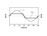
- FIG. 13 is a diagram showing an example of the waveforms of the phase current and the q-axis current by the conventional two-phase modulation.
- FIG. 14 is a diagram showing an example of the waveforms of the phase current and the q-axis current when the power conversion device 100 according to the first embodiment is used. In each figure, the phase current is shown on the upper side, and the q-axis current is shown on the lower side.
- the phase current is the current of any one of the three-phase output currents iu, iv, and iw.
- the q-axis current is a current component that contributes to the motor torque when the phase current is converted into a rotating orthogonal coordinate.
- Figure 14 shows that the distortion of the phase current is suppressed, and the pulsation at three times the frequency is also suppressed. Therefore, by using the power conversion device 100 according to embodiment 1, the current ripple can be suppressed. This makes it possible to suppress the torque ripple generated in the motor 5, and also to suppress the noise caused by the torque ripple. Furthermore, by using the power conversion device 100 according to embodiment 1, the current ripple can be suppressed, and therefore the losses in the wiring resistance and winding resistance caused by the current ripple can be suppressed.
- the power conversion device includes an inverter that converts DC power into AC power and supplies it to a three-phase load, and a control unit that generates switching signals for a plurality of switching elements of three phases provided in the inverter and outputs the switching signals to the inverter.
- the control unit performs two-phase modulation to sequentially suspend the switching operation of the switching elements of one of the three phases, and inserts a three-phase modulation period in which all three phases are switched on immediately before and after the timing when the phase in which the switching operation is suspended during the two-phase modulation transitions from a switching period to a switching suspend period, and immediately before and after the timing when the phase in which the switching operation is suspended transitions from a switching suspend period to a switching period, based on the current flowing in and out of the inverter.
- This control makes it possible to reduce step-like changes in the voltage control error at the timing of transition from the switching period to the switching suspend period and from the switching suspend period to the switching period. This makes it possible to sufficiently suppress ripples in the motor current and motor torque even when a drive method that uses both three-phase modulation and two-phase modulation is adopted.
- the control unit In the power conversion device configured as described above, the control unit generates a first three-phase voltage modulated wave based on a voltage command output from a higher-level control system, and calculates a three-phase common signal for setting a switching pause period while maintaining a line voltage value for the generated first three-phase voltage modulated wave.
- the control unit also calculates a second three-phase voltage modulated wave by superimposing the three-phase common signal on the first three-phase voltage modulated wave.
- the control unit generates a switching signal for the second three-phase voltage modulated wave based on a third three-phase voltage modulated wave in which an error caused by a dead time imparted to the switching signal is corrected.
- the three-phase common signal can be calculated based on a first difference, which is the difference between a first three-phase voltage modulated wave of a value close to a predetermined first limiter value among the first three-phase voltage modulated waves and the first limiter value.
- the three-phase common signal can be calculated based on the second difference, which is the difference between the first three-phase voltage modulation wave close to the first limiter value and the second limiter value whose absolute value is smaller than the first limiter value.
- this third difference can be determined based on at least one of the effective value of the three-phase output current, which is the output current of the inverter, or the voltage-current phase difference, which is the phase difference between the three-phase output voltage, which is the output voltage of the inverter, and the three-phase output current.
- the control unit may perform three-phase modulation without performing two-phase modulation under operating conditions where the rotation speed of the motor is below a predetermined threshold.
- the control unit may not insert a three-phase modulation period under operating conditions where the rotation speed of the motor exceeds a predetermined threshold.
- the control unit may determine the value of the third difference based on the value of the disturbance voltage caused by the dead time under operating conditions where the rotation speed of the motor is below a predetermined threshold, thereby making each phase switch for the entire period of the three-phase modulation period.
- the control unit may not insert a three-phase modulation period for the entire period of the three-phase modulation period by setting the third difference to zero under operating conditions where the rotation speed of the motor exceeds a predetermined threshold.
- Embodiment 2 The magnitude of the disturbance voltage caused by the dead time Td and the Td correction value Vtd, which is the correction voltage value thereof, are generated according to the magnitude of the instantaneous value of the three-phase output currents iu, iv, and iw, as described above.
- the positive and negative polarities of the disturbance voltage and the Td correction value Vtd depend on the polarities of the three-phase output currents iu, iv, and iw
- the remaining margin of the modulation wave operation width also depends on the magnitude and polarity of the three-phase output currents iu, iv, and iw.
- the instantaneous values of the three-phase output currents iu, iv, iw are large, and under conditions in which the polarity of the second three-phase voltage modulated waves Vu2 * , Vv2 * , Vw2 * and the polarity of the Td correction value Vtd, which is its correction voltage value, are the same, the remaining margin of the modulated wave operating range becomes small, and the risk of residual disturbance voltage due to insufficient Td correction increases.
- two-phase modulation and three-phase modulation are switched multiple times within the period of electrical phase angle 0 to 360 degrees. In this way, by switching from two-phase modulation to three-phase modulation in the switching period immediately before or after the switching pause period of two-phase modulation, a voltage operation margin is provided for the three-phase voltage modulation wave.
- control unit 4 switches between two-phase modulation and three-phase modulation multiple times within a period of electrical phase angle 0 to 360 degrees based on at least one of the voltage-current phase difference, the current values of the three-phase output currents iu, iv, iw, the Td correction value Vtd, and the modulation rate.
- a period of three-phase modulation is inserted immediately before or after the switching timing, depending on at least one of the current-voltage phase difference, the current values of the three-phase output currents iu, iv, iw, and the Td correction value Vtd.
- the second three-phase voltage modulated waves Vu2 * , Vv2 * , and Vw2 * may be moved away from the first limiter value Limit1 so that the modulation factor operation corresponding to the Td correction value Vtd can be performed.
- the three-phase modulation insertion period X3in is set based on at least one of the voltage-current phase difference, the current values of the three-phase output currents iu, iv, and iw, the Td correction value Vtd, and the modulation rate, and in the three-phase modulation insertion period X3in, the three-phase common signal Vcom is given as shown in the following formula (10).
- FIGS. 15 and 16 are first and second diagrams for explaining the three-phase modulation insertion period X3in that is inserted by the control according to the second embodiment.
- the same waveforms and elements as those in FIG. 9 are denoted by the same reference numerals.
- Fig. 15 and Fig. 16 in order to avoid complication, only the u-phase voltage modulated wave Vu1 * and the u-phase current iu are shown for the first three-phase voltage modulated wave Vu1* , Vv1 * , Vw1 * and the three-phase output currents iu, iv, iw.
- Fig. 15 shows an example in which the u-phase current iu is ahead of the u-phase voltage modulated wave Vu1 * in phase
- Fig. 16 shows an example in which the u-phase current iu is behind the u-phase voltage modulated wave Vu1 * in phase.
- the three-phase modulation insertion period X3in is shown by a rectangular frame of thick solid lines.
- the periods Xa' and Xb' are provided before and after the u-phase switching pause period Yu in the conventional two-phase modulation so that a suitable voltage operation margin can be obtained.
- the periods Xa' and Xb' shown in FIG. 9 are basically equal in phase angle width.
- the three-phase modulation may be switched to the two-phase modulation at that timing.
- the three-phase modulation is switched to the two-phase modulation at the timing of the zero crossing, so the relationship between the period Xa'' and the period Xb'' is Xa''>Xb''.
- the widths of the periods Xa'', Xb'' and Xa''', Xb''', which are the width of the three-phase modulation insertion period X3in, may be changed according to the Td correction value Vtd in addition to the voltage-current phase difference described above.
- the Td correction value Vtd depends on the magnitude of the current values of the three-phase output currents iu, iv, iw. When the current values of the three-phase output currents iu, iv, iw are small, the operating margin of the modulated wave may be small. Therefore, the widths of the periods Xa'', Xb'', Xa''', Xb''' can be shortened accordingly.
- the widths of the periods Xa'', Xb'', Xa''', and Xb''' can be shortened accordingly.
- the timing of switching may be controlled based on the widths of the periods Xa'', Xb'', Xa''', and Xb''', i.e., the width of the three-phase modulation insertion period X3in.
- the control unit controls the occurrence timing and the occurrence period length of the three-phase modulation period based on at least one of the current value of the three-phase output current of the inverter, the phase difference between the three-phase output voltage and the three-phase output current of the inverter, the voltage correction value for correcting the error caused by the dead time, and the modulation rate of the three-phase output voltage.
- This control makes it possible to eliminate unnecessary voltage operation margin and set the truly necessary width of the three-phase modulation insertion period. This makes it possible to shorten the period in which the three-phase modulation is inserted as much as possible, and to maintain the effect of suppressing switching losses, which is an inherent advantage of two-phase modulation.
- Embodiment 3 a three-phase modulation period in which all three phases are switched is inserted immediately before and after the timing when the phase in which the switching operation is suspended during the implementation of the two-phase modulation transitions from the switching period to the switching suspension period, and immediately before and after the timing when the phase in which the switching operation is suspended transitions from the switching suspension period to the switching period.
- the width of the three-phase modulation insertion period X3in can be further narrowed compared to the first and second embodiments.
- this embodiment will be described with reference to FIG. 17 and FIG. 18.
- FIGS. 17 and 18 are first and second diagrams for explaining the three-phase modulation insertion period X3in that is inserted by the control according to the third embodiment.
- FIG. 17 and FIG. 18 the same waveforms and elements as those in FIG. 15 and FIG. 16 are denoted by the same reference numerals.
- Fig. 17 and Fig. 18 in order to avoid complexity, only the u-phase voltage modulated wave Vu1 * and the u-phase current iu are shown for the first three-phase voltage modulated wave Vu1* , Vv1 * , Vw1 * and the three-phase output currents iu, iv, iw.
- Fig. 17 shows an example in which the u-phase current iu is ahead of the u-phase voltage modulated wave Vu1 * in phase
- Fig. 18 shows an example in which the u-phase current iu is behind the u-phase voltage modulated wave Vu1 * in phase.
- the three-phase modulation insertion period X3in is shown by a rectangular frame of a thick solid line.
- the three-phase modulation insertion period X3in is set only immediately before the timing when the phase for which the switching operation is suspended transitions from the switching period to the switching suspension period, and only immediately before the timing when the phase for which the switching operation is suspended transitions from the switching suspension period to the switching period. Also, in the example of FIG. 18, the three-phase modulation insertion period X3in is set only immediately after the timing when the phase for which the switching operation is suspended transitions from the switching period to the switching suspension period, and only immediately after the timing when the phase for which the switching operation is suspended transitions from the switching suspension period to the switching period.
- the three-phase modulation insertion period X3in is set only immediately before the timing of the transition between the switching period and the switching suspension period, and when the three-phase output currents iu, iv, and iw are in phase with respect to the three-phase output voltage, the three-phase modulation insertion period X3in is set only immediately after the timing of the transition between the switching period and the switching suspension period.
- the three-phase modulation insertion period X3in is inserted only immediately before the timing of the change between the switching period and the switching pause period, but this does not prevent the three-phase modulation insertion period X3in from being set immediately after the change.
- the three-phase modulation insertion period X3in is set only immediately after the timing of the change between the switching period and the switching pause period, but this does not prevent the three-phase modulation insertion period X3in from being set immediately before the change.
- the insertion period of the three-phase modulation can be limited, so that the switching loss can be suppressed while suppressing the current ripple and the torque ripple. In other words, by using the power conversion device according to the third embodiment, it is possible to suppress both the current ripple and the torque ripple and the switching loss.
- the control unit performs two-phase modulation to sequentially suspend the switching operation of the switching elements of one of the three phases, and inserts a three-phase modulation period in which all three phases are switched on at least one of immediately before and after the timing when the phase in which the switching operation is suspended transitions from a switching period to a switching suspension period based on the current flowing in and out of the inverter when performing the two-phase modulation, and at least one of immediately before and after the timing when the phase in which the switching operation is suspended transitions from a switching suspension period to a switching period.
- This control makes it possible to limit the insertion period of the three-phase modulation. This makes it possible to achieve both suppression of current ripple and torque ripple and suppression of switching loss.
- Embodiment 4 In order to maintain the line voltage of the three-phase inverter output, it is necessary to shift the modulated waves of all phases in the same direction, and this shifting operation causes the neutral point potential of the motor 5 to fluctuate. Fluctuations in the neutral point potential have an adverse effect of accelerating the progression of motor shaft electrolytic corrosion, so it is undesirable for the neutral point potential to fluctuate. Therefore, in the fourth embodiment, the fluctuations in the neutral point potential are suppressed while ensuring the accuracy of the Td correction.
- the control according to the fourth embodiment will be described below with reference to FIG. 19.
- FIG. 19 is a diagram for explaining the three-phase modulation insertion period X3in inserted by the control according to the fourth embodiment.
- the three-phase modulation insertion period X3in is shown in a rectangular frame of thick solid lines.
- a three-phase modulation insertion period X3in with an equal phase angle width ⁇ is set before and after the phase angle of 120 degrees at which the u-phase switching pause period Yu in conventional two-phase modulation begins.
- a three-phase modulation insertion period X3in with a predetermined equal phase angle width ⁇ is set before and after the phase angle of 240 degrees at which the u-phase switching pause period Yu in conventional two-phase modulation ends.
- FIG. 19 shows an example of insertion for the u-phase switching pause period Yu, but similar insertion is also performed for the switching pause periods of the v and w phases.
- phase angle widths of the three-phase modulation periods inserted immediately before and after the start of the switching suspension period and immediately before and after the end of the switching suspension period are equal for all four, making it possible to suppress fluctuations in the neutral point potential while ensuring the accuracy of the Td correction.
- three-phase modulation periods of equal phase angle width are inserted at four locations, immediately before and after the start of the switching pause period and immediately before and after the end of the switching pause period, so that it is possible to suppress fluctuations in the neutral point potential while ensuring the accuracy of the Td correction. This makes it possible to suppress the progression of motor shaft electrolytic corrosion while ensuring the accuracy of the Td correction.
- the Td correction value Vtd described in the first embodiment is a voltage corresponding to the magnitude and polarity of the three-phase output current, as shown in Fig. 7 and Fig. 8. Therefore, the closer the phase of the three-phase voltage modulated wave and the phase of the Td correction value Vtd, which is synonymous with the phase of the three-phase output current, the more the symmetry of the three-phase voltage modulated wave is maintained. In order to more suitably suppress the fluctuation of the neutral point potential, a voltage command is generated so that the load power factor becomes 1 with respect to the three-phase output current.
- the method described in Japanese Patent Application Laid-Open No. 10-243700 can be used.
- the motor 5, which is a three-phase load is, for example, a surface permanent magnet type motor
- a method based on a known vector control may be used.
- the three-phase output currents iu, iv, and iw detected by the method of FIG. 1 are coordinate-converted into dq-axis currents Id and Iq on an orthogonal coordinate system that rotates in synchronization with the rotor of the motor 5, and a d-axis current command Id * and a q-axis current command Iq * are generated.
- a voltage command for each axis is generated based on the difference between the dq-axis current commands Id * and Iq * and the coordinate-converted detected current values Id and Iq in each of the d and q axes.
- the d-axis current command Id * is given zero, and the d-axis current Id is controlled to be zero, so that the load power factor can be controlled to 1 more accurately. Therefore, if the motor 5 is a surface permanent magnet type motor, the load power factor can be suitably controlled to 1 by using this type of vector control.
- the control unit controls the load power factor to approach 1 according to the three-phase output current, which is the output current of the inverter.
- the load power factor By controlling the load power factor to approach 1, the phase difference between each phase in the three-phase output current and the three-phase output voltage approaches zero, so that the switching pause period due to two-phase modulation coincides with the period in which each phase current is large. Since the switching loss reduction effect has the property of being approximately proportional to the magnitude of the three-phase output current, in addition to the effects described in the first to fourth embodiments, the switching loss reduction effect can be enhanced.
- the load power factor can be strictly controlled to 1 by controlling the d-axis current command to zero, so that the switching loss reduction effect can be further enhanced.
- Embodiment 6. 20 is a diagram showing a configuration example of an air conditioning apparatus 200 according to embodiment 6.
- the air conditioning apparatus 200 according to embodiment 6 includes the power conversion apparatus 100 described in embodiments 1 to 5, a compressor 50, a fan motor 5b, a fan 52 driven by the fan motor 5b, and a refrigeration cycle 110.
- the compressor 50 includes a compressor motor 5a and a compression element 51 that compresses the refrigerant.
- the compressor motor 5a is the drive source of the compressor 50.
- the power conversion device 100 has two inverters (not shown) that supply power to the compressor motor 5a, which is the drive source for the compressor 50, and the fan motor 5b, which is the drive source for the fan 52. At least one of the two inverters is the inverter 3 described in the first to fifth embodiments.
- the purpose of the converter 2 described in the first to fifth embodiments is to output a rectified voltage, and it may be common to the two inverters 3, or may be provided separately for each of the two inverters 3.
- a refrigerant circuit is formed by a compressor 50, a four-way valve 121, a heat source side heat exchanger 122, a load side heat exchanger 132, and an expansion device 131.
- the compressor 50 compresses the refrigerant, the heat source side heat exchanger 122 and the load side heat exchanger 132 exchange heat of the refrigerant, and a fan 52 blows air to the heat source side heat exchanger 122.
- FIG. 20 shows a configuration in which the four-way valve 121 and the heat source side heat exchanger 122 are provided in the outdoor unit 120, and the expansion device 131 and the load side heat exchanger 132 are provided in the indoor unit 130. Note that the configuration in FIG. 20 is an example, and the air conditioning device 200 according to the sixth embodiment is not limited to the configuration in FIG. 20.
- the current ripple of at least one of the compressor motor 5a, which is the driving source of the compressor 50, and the fan motor 5b, which is the driving source of the fan 52, is suppressed, and therefore the torque ripple generated by the motor is suppressed.
- Fig. 21 is a diagram showing an example of a hardware configuration for realizing the functions of the control unit 4 in embodiments 1 to 5.
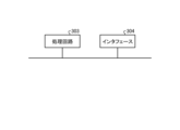
- Fig. 22 is a diagram showing another example of a hardware configuration for realizing the functions of the control unit 4 in embodiments 1 to 5.
- the configuration can include a processor 300 that performs calculations, a memory 302 that stores programs read by the processor 300, and an interface 304 that inputs and outputs signals, as shown in FIG. 21.
- Processor 300 is an example of a computing means.
- Processor 300 may be a computing means called a microprocessor, a microcomputer, a CPU (Central Processing Unit), or a DSP (Digital Signal Processor).
- Examples of memory 302 include non-volatile or volatile semiconductor memory such as RAM (Random Access Memory), ROM (Read Only Memory), flash memory, EPROM (Erasable Programmable ROM), and EEPROM (registered trademark) (Electrically EPROM), magnetic disks, flexible disks, optical disks, compact disks, mini disks, and DVDs (Digital Versatile Discs).
- Memory 302 stores a program that executes the functions of control unit 4 in embodiments 1 to 5.
- Processor 300 receives and transmits necessary information via interface 304, executes the program stored in memory 302, and refers to the table stored in memory 302, thereby performing the above-mentioned processing.
- the results of calculations by processor 300 can be stored in memory 302.
- the processing circuit 303 shown in FIG. 22 can be used.
- the processing circuit 303 can be a single circuit, a composite circuit, an ASIC (Application Specific Integrated Circuit), an FPGA (Field-Programmable Gate Array), or a combination of these.
- Information input to the processing circuit 303 and information output from the processing circuit 303 can be exchanged via an interface 304.
- control unit 4 may be performed by the processing circuit 303, and other processing that is not performed by the processing circuit 303 may be performed by the processor 300 and memory 302.
- the number of phases of the commercial power supply 1, which is an AC power supply may be either single-phase or three-phase.
- the commercial power supply 1 and converter 2 operate as DC power supply sources that supply DC power to the inverter 3, but a DC power supply such as a battery may be used instead of the commercial power supply 1 and converter 2.
- the modulation factor command Vk and voltage phase ⁇ input to the control unit 4 are generated based on current feedback control including vector control, which is well known in a higher-level control system, or feedforward control.
- the explanation is based on the assumption that a bottom-attached two-phase modulation method is used, but the same can be achieved by using a top-attached two-phase modulation method in which the upper limit value is set to "1" and attached to the upper limit value side.
- 1 Commercial power supply 2 Converter, 3 Inverter, 4 Control unit, 5 Motor, 5a Compressor motor, 5b Fan motor, 6a, 6b, 7 Electrical wiring, 31a-31c, 32a-32c Switching elements, 33a-33c, 34 Shunt resistor, 35a, 35b Current detector, 41, 41A Modulation method selection unit, 42 Modulation wave generation unit, 43 Td correction unit, 44 PW M modulation section, 45 Td addition section, 50 compressor, 51 compression element, 52 fan, 100 power conversion device, 110 refrigeration cycle, 120 outdoor unit, 121 four-way valve, 122 heat source side heat exchanger, 130 indoor unit, 131 expansion device, 132 load side heat exchanger, 200 air conditioning device, 300 processor, 302 memory, 303 processing circuit, 304 interface.
Landscapes
- Engineering & Computer Science (AREA)
- Power Engineering (AREA)
- Inverter Devices (AREA)
Priority Applications (2)
| Application Number | Priority Date | Filing Date | Title |
|---|---|---|---|
| JP2025533799A JPWO2025017870A1 (https=) | 2023-07-19 | 2023-07-19 | |
| PCT/JP2023/026425 WO2025017870A1 (ja) | 2023-07-19 | 2023-07-19 | 電力変換装置及び空気調和装置 |
Applications Claiming Priority (1)
| Application Number | Priority Date | Filing Date | Title |
|---|---|---|---|
| PCT/JP2023/026425 WO2025017870A1 (ja) | 2023-07-19 | 2023-07-19 | 電力変換装置及び空気調和装置 |
Publications (1)
| Publication Number | Publication Date |
|---|---|
| WO2025017870A1 true WO2025017870A1 (ja) | 2025-01-23 |
Family
ID=94281312
Family Applications (1)
| Application Number | Title | Priority Date | Filing Date |
|---|---|---|---|
| PCT/JP2023/026425 Pending WO2025017870A1 (ja) | 2023-07-19 | 2023-07-19 | 電力変換装置及び空気調和装置 |
Country Status (2)
| Country | Link |
|---|---|
| JP (1) | JPWO2025017870A1 (https=) |
| WO (1) | WO2025017870A1 (https=) |
Citations (4)
| Publication number | Priority date | Publication date | Assignee | Title |
|---|---|---|---|---|
| JPH09149660A (ja) * | 1995-11-27 | 1997-06-06 | Toshiba Corp | Pwm制御インバータの制御装置 |
| WO2005057771A1 (ja) * | 2003-12-15 | 2005-06-23 | Matsushita Electric Industrial Co., Ltd. | モータ駆動装置 |
| JP2013162529A (ja) * | 2012-02-01 | 2013-08-19 | Fanuc Ltd | 変調方式の選択部を有するモータ駆動用のpwm整流器 |
| JP2017184535A (ja) * | 2016-03-31 | 2017-10-05 | アイシン・エィ・ダブリュ株式会社 | インバータ制御装置 |
-
2023
- 2023-07-19 WO PCT/JP2023/026425 patent/WO2025017870A1/ja active Pending
- 2023-07-19 JP JP2025533799A patent/JPWO2025017870A1/ja active Pending
Patent Citations (4)
| Publication number | Priority date | Publication date | Assignee | Title |
|---|---|---|---|---|
| JPH09149660A (ja) * | 1995-11-27 | 1997-06-06 | Toshiba Corp | Pwm制御インバータの制御装置 |
| WO2005057771A1 (ja) * | 2003-12-15 | 2005-06-23 | Matsushita Electric Industrial Co., Ltd. | モータ駆動装置 |
| JP2013162529A (ja) * | 2012-02-01 | 2013-08-19 | Fanuc Ltd | 変調方式の選択部を有するモータ駆動用のpwm整流器 |
| JP2017184535A (ja) * | 2016-03-31 | 2017-10-05 | アイシン・エィ・ダブリュ株式会社 | インバータ制御装置 |
Also Published As
| Publication number | Publication date |
|---|---|
| JPWO2025017870A1 (https=) | 2025-01-23 |
Similar Documents
| Publication | Publication Date | Title |
|---|---|---|
| JP3971979B2 (ja) | 空気調和装置 | |
| US11139771B2 (en) | Control device and control method for AC motor and AC motor drive system | |
| US9287820B2 (en) | Motor control device and air conditioner | |
| JP5718474B2 (ja) | 電力変換装置、電動機駆動装置および空調機 | |
| JP7361222B2 (ja) | オープン巻線モータ駆動装置 | |
| KR101514391B1 (ko) | 벡터 제어 장치, 및 그것을 사용한 모터 제어 장치, 공조기 | |
| WO2013080610A1 (ja) | 電力変換装置、電動機駆動装置及び空気調和機 | |
| JP7341359B2 (ja) | 電力変換装置、モータ駆動装置及び冷凍サイクル適用機器 | |
| JP2002247876A (ja) | インバータ装置、圧縮機制御装置、冷凍・空調装置の制御装置、モータの制御方法、圧縮機、冷凍・空調装置 | |
| JP7527485B2 (ja) | インバータ制御装置、インバータ制御方法 | |
| JP5078925B2 (ja) | 電動機の駆動装置並びに機器 | |
| JP7332382B2 (ja) | インバータ装置 | |
| JP2014138526A (ja) | インバータ制御装置およびインバータ制御装置を備える圧縮機 | |
| WO2025017870A1 (ja) | 電力変換装置及び空気調和装置 | |
| JP3490600B2 (ja) | 電力変換装置のパルス幅変調方法 | |
| JP7523693B2 (ja) | 電力変換器の制御部および電力変換装置 | |
| US20260078914A1 (en) | Motor drive device, air-sending device, air-conditioning apparatus, and motor driving method | |
| JP6695028B2 (ja) | 整流回路装置 | |
| CN110326210B (zh) | 空调机 | |
| JP7361948B2 (ja) | 電動機駆動装置、冷凍サイクル装置、及び空気調和機 | |
| CN104009692A (zh) | 马达控制装置以及使用了该马达控制装置的空调机 | |
| WO2024105859A1 (ja) | インバータ制御装置、モータ駆動装置、送風機及び空気調和機 | |
| WO2024023920A1 (ja) | インバータ制御装置、モータ駆動装置、送風機及び空気調和機 | |
| TW202604123A (zh) | 電力控制裝置、電力控制方法、以及空氣調節機 | |
| WO2026083643A1 (ja) | 電力変換装置 |
Legal Events
| Date | Code | Title | Description |
|---|---|---|---|
| 121 | Ep: the epo has been informed by wipo that ep was designated in this application |
Ref document number: 23945873 Country of ref document: EP Kind code of ref document: A1 |
|
| WWE | Wipo information: entry into national phase |
Ref document number: 2025533799 Country of ref document: JP |
|
| NENP | Non-entry into the national phase |
Ref country code: DE |