WO2025013174A1 - 配線基板 - Google Patents
配線基板 Download PDFInfo
- Publication number
- WO2025013174A1 WO2025013174A1 PCT/JP2023/025464 JP2023025464W WO2025013174A1 WO 2025013174 A1 WO2025013174 A1 WO 2025013174A1 JP 2023025464 W JP2023025464 W JP 2023025464W WO 2025013174 A1 WO2025013174 A1 WO 2025013174A1
- Authority
- WO
- WIPO (PCT)
- Prior art keywords
- pattern
- measurement
- measurement electrode
- wiring board
- moisture
- Prior art date
- Legal status (The legal status is an assumption and is not a legal conclusion. Google has not performed a legal analysis and makes no representation as to the accuracy of the status listed.)
- Ceased
Links
Images









Classifications
-
- G—PHYSICS
- G01—MEASURING; TESTING
- G01R—MEASURING ELECTRIC VARIABLES; MEASURING MAGNETIC VARIABLES
- G01R31/00—Arrangements for testing electric properties; Arrangements for locating electric faults; Arrangements for electrical testing characterised by what is being tested not provided for elsewhere
- G01R31/28—Testing of electronic circuits, e.g. by signal tracer
-
- H—ELECTRICITY
- H05—ELECTRIC TECHNIQUES NOT OTHERWISE PROVIDED FOR
- H05K—PRINTED CIRCUITS; CASINGS OR CONSTRUCTIONAL DETAILS OF ELECTRIC APPARATUS; MANUFACTURE OF ASSEMBLAGES OF ELECTRICAL COMPONENTS
- H05K1/00—Printed circuits
- H05K1/02—Details
-
- H—ELECTRICITY
- H05—ELECTRIC TECHNIQUES NOT OTHERWISE PROVIDED FOR
- H05K—PRINTED CIRCUITS; CASINGS OR CONSTRUCTIONAL DETAILS OF ELECTRIC APPARATUS; MANUFACTURE OF ASSEMBLAGES OF ELECTRICAL COMPONENTS
- H05K3/00—Apparatus or processes for manufacturing printed circuits
Definitions
- This disclosure relates to a wiring board.
- Wiring boards such as printed wiring boards usually contain a resin base material (which has water absorption properties). Therefore, the wiring board absorbs moisture. When the wiring board absorbs moisture, the dielectric constant of the wiring board changes. The change in dielectric constant leads to a change in impedance. When the impedance of the wiring board changes, malfunctions occur in the circuit in which the wiring board is used.
- Patent Document 1 Technology for detecting malfunctions in wiring boards is known (see, for example, Patent Document 1).
- wiring is formed on the wiring board to detect abnormalities in advance.
- Prevention of wiring boards refers to preventing the change in impedance of a wiring board from exceeding the allowable range.
- An example of prevention of wiring boards is recovering wiring boards whose impedance has changed and replacing them with wiring boards that have normal impedance.
- Maintaining a wiring board means preventing any further change in impedance for a wiring board whose impedance has changed within the allowable range.
- Preventive maintenance and repair of wiring boards is especially important after the wiring board has been incorporated into a product and the product has been shipped. This is because the environments in which shipped products are placed vary widely and because products are used for a long period of time.
- the present disclosure therefore aims to provide a wiring board that allows for appropriate prevention and maintenance even after a product incorporating the wiring board has been shipped.
- the wiring board of the present disclosure comprises a measurement electrode pair including two measurement electrodes arranged with at least a portion of a resin base material sandwiched therebetween, and a through hole penetrating the resin base material in a thickness direction of the resin base material, the through hole being arranged at least partially around the measurement electrodes in a plan view, the measurement electrode pair including a first measurement electrode pair and a second measurement electrode pair, and when the measurement electrode included in the first measurement electrode pair is defined as a first measurement electrode and the measurement electrode included in the second measurement electrode pair is defined as a second measurement electrode, A moisture-proof layer is formed on a side surface of the through hole arranged around the first measurement electrode, and the resin substrate is exposed from a side surface of the through hole arranged around the second measurement electrode.
- the wiring board disclosed herein can provide a wiring board that allows for appropriate prevention and maintenance even after the product into which the wiring board is incorporated has been shipped.
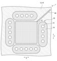
- FIG. 2 is a plan view of a wiring board having a pattern A.
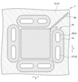
- FIG. 13 is a plan view of the wiring board of pattern B.
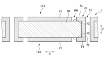
- FIG. 2 is a perspective view of a wiring board of pattern A.
- FIG. 13 is a perspective view of a wiring board of pattern B.
- 5 is a diagram showing the relationship between the length of each portion of the wiring board and the impedance.
- FIG. 4 is a diagram showing the relationship between the length and the dielectric constant of each portion of the wiring board.
- FIG. 11A and 11B are diagrams illustrating an example of a change in the dielectric constant of a wiring substrate.
- FIG. 11 is a diagram showing an example of change in dielectric constant of a conventional wiring board.
- FIG. 13 is a diagram showing a first modified example of the conductor arrangement of pattern A.
- FIG. 13 is a diagram showing a first modified example of the conductor arrangement of pattern B.
- FIG. 13 is a diagram showing a second modification of the conductor arrangement of pattern A.
- FIG. 13 is a diagram showing a second modification of the conductor arrangement of pattern B.
- FIG. 13 is a diagram showing a third modified example of the conductor arrangement of pattern A.
- FIG. 13 is a diagram showing a third modified example of the conductor arrangement of pattern B.
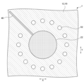
- FIG. 13 is a diagram showing a fourth modified example of the conductor arrangement of pattern A.
- FIG. 13 is a diagram showing the relationship between the length of each portion of the wiring board and the impedance.
- FIG. 5 is a diagram showing a fifth modified example of the conductor arrangement of pattern A.
- FIG. 5 is a diagram showing a fifth modified example of the conductor arrangement of pattern B.
- FIG. 6 is a diagram showing a sixth modified example of the conductor arrangement of pattern A.
- FIG. 6 is a diagram showing a sixth modified example of the conductor arrangement of pattern B.
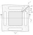
- Figs. 1 and 2 are plan views of wiring board 1.
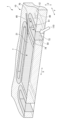
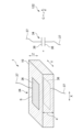
- Figs. 3 and 4 are perspective views of wiring board 1.
- Fig. 3 shows a cross section taken along line 100-100 in Fig. 1.
- Fig. 4 shows a cross section taken along line 102-102 in Fig. 2.
- the figure shows an XYZ Cartesian coordinate system.
- the X, Y, and Z directions are the same in each figure.
- the Z direction is the thickness direction of the wiring board 1. If there is a straight edge on the outer periphery of the measuring electrode (described later), the X direction is a direction parallel to that edge.
- FIG. 1 shows a first measuring electrode 21, which is an example of a measuring electrode.
- the first measuring electrode 21 has an outer periphery 211 that extends in a straight line. Therefore, the direction parallel to the direction in which the outer periphery 211 extends is defined as the X direction.
- FIGS. 1 and 2 show a surface of wiring board 1 parallel to the XY plane.
- FIGS. 3 and 4 show a cross section of wiring board 1 parallel to the XZ plane. Viewing wiring board 1 from the Z direction is called a planar view.
- the wiring board 1 includes a resin base material 10 and a conductor.
- the resin base material 10 is a substrate formed from resin.
- the resin base material 10 functions as an insulating layer.
- the conductor is a conductor that is placed on the surface of the resin substrate 10.
- the conductor is placed on the resin substrate 10 in various forms. Examples of forms include electrodes, wiring, and through-hole plating.
- the conductor is formed from copper foil or the like.
- the conductors are arranged on the wiring board 1 in at least two types of conductor arrangement patterns.
- One pattern is called pattern A.
- the other pattern is called pattern B.
- Pattern A is a pattern that inhibits moisture absorption by the resin base material 10.
- Pattern B is a pattern that promotes moisture absorption by the resin base material 10.
- Figures 1 and 3 show the conductor arrangement of pattern A.
- Figures 2 and 4 show the conductor arrangement of pattern B.
- the conductor arrangement of pattern A and the conductor arrangement of pattern B both include a measurement electrode pair and a through hole, i.e., a cut hole.
- the measurement electrode pair includes two measurement electrodes arranged to face each other with the resin substrate 10 in between.
- the measurement electrodes are formed of copper foil. These two measurement electrodes constitute an electrode pair.
- the measurement electrode pair included in pattern A is referred to as the first measurement electrode pair 7.
- the measurement electrode pair included in pattern B is referred to as the second measurement electrode pair 9.
- the two measurement electrodes included in the first measurement electrode pair 7 are referred to as first measurement electrodes 21.
- the two measurement electrodes included in the second measurement electrode pair 9 are referred to as second measurement electrodes 22.
- the cut holes are through holes that penetrate the resin substrate 10.
- the cut holes penetrate the resin substrate 10 in the thickness direction Z of the resin substrate 10.
- the cut holes included in pattern A are called first cut holes 51.
- the cut holes included in pattern B are called second cut holes 52.
- Pattern A and pattern B differ in whether or not a moisture-proof layer 70 is provided in the cut hole.
- the resin substrate 10 is exposed from the side of the cut hole.
- the resin substrate 10 is prone to absorbing moisture.
- the moisture-proof layer 70 is a layer that prevents the resin substrate 10 from absorbing moisture through the cut holes.
- the moisture-proof layer 70 is formed on the sides of the cut holes and around the cut holes on the surface layer of the resin substrate 10.
- the moisture-proof layer 70 will be described in detail later.
- the moisture-proof layer 70 is formed from copper foil or the like.
- the copper foil prevents moisture from passing through.
- the copper foil can be formed by plating or the like.
- the cut hole promotes moisture absorption in the resin substrate 10 compared to a resin substrate without a cut hole.
- the moisture-proof layer 70 inhibits moisture absorption in the resin substrate 10.
- a moisture-proof layer 70 is provided in the first cut hole 51 of pattern A. Pattern A functions as a moisture absorption inhibition pattern. A moisture-proof layer 70 is not provided in the second cut hole 52 of pattern B. Pattern B functions as a moisture absorption promotion pattern.
- Pattern A will be specifically described with reference to Fig. 1 and Fig. 3. As shown in Fig. 3, pattern A includes a first measurement electrode pair 7.
- the first measurement electrode pair 7 includes two first measurement electrodes 21.
- the two first measurement electrodes 21 are arranged to face each other with the resin substrate 10 interposed therebetween.
- the shape of the first measurement electrode 21 is quadrangular (rectangular) in a plan view.
- First cutouts 51 are formed near the four sides of the first measurement electrode 21.
- the first cutouts 51 are formed near each of the four sides of the first measurement electrode 21.
- the first cutouts 51 extend in the X direction or the Y direction.
- the first cut hole 51 is a through hole formed in the resin substrate 10.
- the first cut hole 51 is a hole formed by removing the resin substrate 10 in the thickness direction of the resin substrate 10.
- the thickness direction of the resin substrate 10 is the Z direction.
- the shape of the first cut hole 51 is an elongated hole in a plan view. The longitudinal direction of the elongated hole shape is parallel to the direction in which the outer edge of the first measurement electrode 21 extends.
- a moisture-proof layer 70 is formed in the first cutout 51.
- the moisture-proof layer 70 is formed of copper foil.
- the moisture-proof layer 70 includes a side moisture-proof layer 72 and a surface moisture-proof layer 74. As shown in FIG. 3, the side moisture-proof layer 72 is the moisture-proof layer 70 formed on the side 54 of the first cutout 51.
- the side 54 of the first cutout 51 is the inner wall surface of a through hole formed in the resin substrate 10.
- the surface moisture-proof layer 74 is a moisture-proof layer 70 formed on the surface layer 12 of the resin substrate 10.
- the side moisture barrier layer 72 is formed to cover the entire side surface 54 of the first cutout 51. By covering the entire side surface 54 with the side moisture barrier layer 72, it is possible to prevent the resin substrate 10 from absorbing moisture through the side surface 54.
- the surface moisture-proof layer 74 is positioned so as to cover the periphery of the first cutout 51 in plan view.
- the side moisture barrier layer 72 and the surface moisture barrier layer 74 are continuous.
- the side moisture barrier layer 72 and the surface moisture barrier layer 74 are continuous means that the resin substrate 10 is not exposed between the side moisture barrier layer 72 and the surface moisture barrier layer 74.
- the surface moisture barrier layer 74 is formed to surround the first cut hole 51 in a plan view. Therefore, the shape of the surface moisture barrier layer 74 is ring-shaped in a plan view.
- gaps 106 and 108 are also portions where no conductor is formed, similar to gap 104.
- first cut holes 51 are formed.
- a surface moisture barrier layer 74 is formed in each of the four first cut holes 51. Therefore, four surface moisture barrier layers 74 are formed along the outer edge of the first measurement electrode 21.
- a measurement lead-out wiring 40 is formed on the surface layer 12 of the resin substrate 10.
- the measurement lead-out wiring 40 is a connection wiring used when measuring the capacitance of the first measurement electrode pair 7.
- the measurement lead-out wiring 40 is connected at one end to the first measurement electrode 21.
- Pattern B will be described with reference to Fig. 2 and Fig. 4. The differences between pattern B and pattern A will be mainly described. For points that are not described, the description of pattern A will be used. Pattern B is similar to pattern A except that the moisture-proof layer 70 is not formed.
- pattern B includes a second measurement electrode pair 9.
- the second measurement electrode pair 9 includes two second measurement electrodes 22.
- the two second measurement electrodes 22 are arranged to face each other with the resin substrate 10 in between.
- the shape of the second measurement electrode 22 is quadrangular (rectangular) in a plan view. Second cutouts 52 are formed near the four sides of the second measurement electrode 22.
- the shape of the second measurement electrode pair 9 included in pattern B is the same as the shape of the first measurement electrode pair 7 included in pattern A.
- the shape of the second cutout 52 included in pattern B is the same as the shape of the first cutout 51 included in pattern A.
- the moisture-proof layer 70 is not formed in the second cut hole 52. Therefore, as shown in FIG. 4, the resin substrate 10 is exposed from the side surface 54 of the second cut hole 52.
- pattern A and pattern B differ in the presence or absence of a moisture-proof layer 70.
- a moisture-proof layer 70 is formed. Therefore, moisture absorption by the resin substrate 10 from the side surface 54 of the cut hole, as shown by the arrow 110 in FIG. 3, is inhibited.
- Pattern A has a conductor arrangement that inhibits moisture absorption.
- Pattern B the moisture-proof layer 70 is not formed. Therefore, as shown by the arrow 112 in FIG. 4, the resin base material 10 absorbs moisture from the side surface 54 of the cut hole. The moisture absorption of the wiring board 1 is promoted by the addition of moisture absorption from the side surface 54 of the cut hole.
- Pattern B is a conductor arrangement that promotes moisture absorption.
- pattern A which is a pattern that inhibits moisture absorption
- pattern B which is a pattern that promotes moisture absorption
- W is the length in the X direction of the measurement model electrode 32 formed on the surface layer 12 of the resin base material 10.
- t is the length in the Z direction of the measurement model electrode 32.
- t is equal to the thickness of the measurement model electrode 32.
- h is the length in the Z direction of the resin base material 10.
- h is equal to the thickness of the resin base material 10.
- a counter electrode 30 is formed on the surface of the resin substrate 10 facing the surface layer 12.
- the counter electrode 30 faces the measurement model electrode 32 across the resin substrate 10.
- the distance between the measurement model electrode 32 and the counter electrode 30 is the above-mentioned h.
- ⁇ r is the relative dielectric constant of the resin base material 10. Even if the wiring board 1 absorbs moisture, the thickness h of the resin base material 10, the length W of the measurement model electrode 32 in the X direction, and the thickness t of the measurement model electrode 32 do not change. Therefore, as shown in equation 120 in FIG. 5, the relative dielectric constant ⁇ r of the resin base material 10 and the impedance Z0 of the wiring board 1 are correlated.
- Fig. 6 is a diagram showing the relationship between the length of each part of the wiring board 1 and the dielectric constant ⁇ of the resin base material 10.
- the dielectric constant ⁇ of the resin base material 10 can be measured using a pair of measuring electrodes formed on the wiring board 1. Specifically, the dielectric constant ⁇ of the resin base material 10 can be measured using a first pair of measuring electrodes 7 in pattern A, and using a second pair of measuring electrodes 9 in pattern B.
- the impedance Z0 of the wiring board 1 can be calculated using equation 120 in Fig. 5.
- the two measurement electrodes included in the measurement model electrode pair 34 shown in FIG. 6 are referred to as the measurement model electrodes 36.
- the two measurement model electrodes 36 are arranged to face each other with the resin substrate 10 in between.
- a wiring 37 is connected to the measurement model electrodes 36.
- S shown in FIG. 6 is the area of the measurement model electrode 36.
- d is the length of the resin substrate 10 in the Z direction. d is equal to the thickness of the resin substrate 10. Also, d is the distance between the two measurement model electrodes 36.
- C is the capacitance of the resin substrate 10.
- ⁇ is the dielectric constant of the resin substrate 10.
- the measurement model electrode pair 34 formed on the wiring board 1 is equivalent to a capacitor.
- the measurement model electrode pair 34 is charged via the wiring 37, and the capacitance C of the resin substrate 10 is measured by measuring the potential difference between the two measurement model electrodes 36. Then, the dielectric constant ⁇ of the resin substrate 10 is calculated based on the formula 122 in FIG. 6.
- the impedance Z 0 of the wiring board 1 can be determined by equation 120 in FIG.
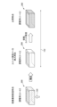
- Figure 7 is a diagram showing the dielectric constant at each distribution stage for each conductor arrangement pattern.
- Figure 7 shows three distribution stages: the time of wiring board manufacture, the time of delivery to the unit manufacturer, and the field.
- the field refers to the market where the unit is shipped.
- Wiring board 1 includes within a single wiring board the conductor arrangement of pattern A, which is a moisture absorption inhibiting pattern, and the conductor arrangement of pattern B, which is a moisture absorption promoting pattern. Therefore, by measuring the difference in dielectric constant between pattern A, which inhibits moisture absorption, and pattern B, which promotes moisture absorption, it is possible to confirm the change in dielectric constant due to moisture absorption.
- the moisture absorption-promoting pattern B has a structure that absorbs moisture faster than functional areas within the wiring board 1. That is, by opening through holes in the resin base material 10, the area of the resin base material 10 that comes into direct contact with the air is increased, and the resin base material 10 has a structure that makes it easier to absorb moisture. This makes it possible to realize a structure that makes it easy to raise an alert as a preventative and maintenance measure. In other words, changes in the state of the wiring board 1 due to moisture absorption can be confirmed early and accurately.
- the wiring board 1 is transported to the unit manufacturer.
- the dielectric constant of the resin base material 10 of pattern A is 3.8.
- the dielectric constant of the resin base material 10 of pattern B is 4.0.
- the dielectric constant of the resin base material 10 of pattern A has not changed since the wiring board was manufactured.
- the dielectric constant of the resin base material 10 of pattern B has increased by 0.2 since the wiring board was manufactured. Since pattern A is a moisture absorption inhibiting pattern, the resin base material 10 does not absorb moisture. Since pattern B is a moisture absorption promoting pattern, the resin base material 10 absorbs moisture.
- pattern A the resin substrate 10 does not absorb moisture, so it is thought that the dielectric constant will not change.
- pattern B the resin substrate 10 absorbs moisture, so it is thought that the dielectric constant will increase.
- the wiring board 1 is then shipped and sent to the field.
- the dielectric constant of the resin base material 10 of pattern A is 3.8.
- the dielectric constant of the resin base material 10 of pattern B is 4.2.
- the dielectric constant of the resin base material 10 of pattern A has not changed since the time of wiring board manufacture. This is thought to be because pattern A is a moisture absorption inhibiting pattern, so the resin base material 10 does not absorb moisture.
- the dielectric constant of the resin base material 10 of pattern B is 4.2.
- the dielectric constant of the resin base material 10 of pattern B has increased by a further 0.2 since the time of delivery to the unit manufacturer. It is thought that the moisture absorption of the resin base material 10 has progressed further in pattern B.
- the dielectric constant of pattern A does not change from the time the wiring board is manufactured until it is in the field. Therefore, even if the dielectric constant at the time the wiring board is manufactured is unknown, the moisture absorption state of the resin base material 10 can be confirmed by evaluating the difference in the dielectric constant of pattern B relative to the dielectric constant of pattern A at each point in time.
- Figure 8 is a diagram showing an example of the change in dielectric constant in a conventional wiring board 200.
- the conventional wiring board 200 two patterns of conductor arrangements, a moisture absorption promotion pattern and a moisture absorption inhibition pattern for comparison with the moisture absorption promotion pattern, are not formed in a single wiring board 200. Therefore, it is not possible to obtain a reference value for checking the moisture absorption state from the wiring board 200.
- the unit manufacturer usually cannot grasp the dielectric constant of the wiring board 200 at the time of wiring board manufacture.
- the period during which the unit manufacturer can measure the dielectric constant of the wiring board 200 is, for example, the period shown by arrow 132 in FIG. 8.
- the unit manufacturer can measure the dielectric constant from the time the wiring board 200 is delivered, to the time the unit is manufactured using the wiring board 200, and the time the unit is shipped.
- the dielectric constant at the time of wiring board manufacture shown by arrow 130 in FIG. 8, cannot be measured.
- the conventional wiring board 200 it is difficult to accurately check the moisture absorption state of the resin base material.
- the dielectric constant at the time of shipment is 4.3, it is difficult to accurately determine whether or not this value is a problem from the perspective of moisture absorption of the resin base material. This is because the dielectric constant of the resin base material in an unabsorbed state is required to accurately determine the moisture absorption state of the resin base material.
- the moisture absorption state of the resin base material 10 can be accurately confirmed at any time based on a reference value.
- the wiring board 1 includes pattern A, which inhibits moisture absorption. Therefore, for example, when the difference between the dielectric constant of pattern B and the dielectric constant of pattern A becomes large, that is, when the increase in the dielectric constant of pattern B becomes large, it is possible to determine that the moisture absorption of the resin base material 10 has increased and issue an alert.
- the above describes an example of a configuration of the wiring board 1 in which the first measurement electrode 21 and the second measurement electrode 22 have a rectangular shape in a plan view. Also, a description has been given of a case in which the shape of the cutout in a plan view is an elongated hole.
- the shapes of the measurement electrodes and the cutout are not limited to this. Below, modified examples of the measurement electrodes and the cutout are described.
- FIG. 9 is a diagram showing a first modified example of pattern A.
- Figure 10 is a diagram showing a first modified example of pattern B. In the following description of each modified example, differences from the conductor arrangement described with reference to Figures 1 to 4 will be mainly described.
- first cut hole 51 and the second cut hole 52 will be simply referred to as cut holes.
- the shapes of the first cut hole 51 and the second cut hole 52 will be simply referred to as cut hole shapes.
- the shape of the cut hole is an elongated hole when viewed from above.
- the shape of the cut hole is a circular hole when viewed from above.
- Peeling of the conductor refers to the peeling of lands, pads, electrodes, etc.
- round holes are formed in place of the single cut hole of the basic example.
- This number of round holes is an example. Any number of round holes can be formed in place of the single cut hole of Figure 1.
- the arrangement of the round holes is not limited to a single linear row. The arrangement of the round holes can be, for example, two or more rows.
- FIG. 11 is a diagram showing a second modification of the pattern A.
- Fig. 12 is a diagram showing a second modification of the pattern B.
- the long holes constituting the cutouts were formed near each outer edge of the first measurement electrode 21 and each outer edge of the second measurement electrode 22, one each.
- two long holes are formed near each outer edge. Therefore, the length of the long side of the long hole in modified example 2 is shorter than the length of the long side of the long hole in the basic example.
- two long holes are formed instead of the one long hole of the basic example.
- This number of long holes is an example.
- the number of small long holes formed in place of the one long hole of the basic example can be set to any number equal to or greater than two.
- the size of the oblong holes to be formed does not have to be uniform.
- oblong holes with different lengths of the long side may be formed, such as oblong holes 56 and 57 shown in FIG. 11.
- FIG. 13 is a diagram showing a third modification of the pattern A.
- Fig. 14 is a diagram showing a third modification of the pattern B.
- the cut holes are formed only as long holes.
- the cut holes are formed as long holes and round holes.
- the long hole is usually formed by drilling a round hole multiple times. When drilling multiple times, misalignment may occur. In addition, in order to withstand multiple drillings, it is preferable that the resin substrate 10 around the area where the long hole is to be formed has sufficient rigidity.
- the design distance between the long hole and other cut holes, and the design distance between the long hole and the measurement electrode, etc. are longer than in the case of a round hole.
- the part around this hole that provides support etc. is called the remaining allowance. Cut holes are usually not formed in the remaining allowance.
- the remaining space left when the cutting hole is completed can be made smaller.
- the round hole is formed after the long hole is formed in the remaining space when the long hole is formed.
- the surrounding resin base material 10 does not require as much rigidity as when a long hole is formed. Therefore, the remaining space in the round hole may be smaller than the remaining space in the long hole.
- a round hole is formed in the remaining space for the long hole, so that the remaining space remaining after forming the cut hole can be reduced.
- the remaining space is the portion where the cut hole is not formed.
- a smaller remaining space means that a longer cut hole is formed near each outer edge of the first measurement electrode 21 and the second measurement electrode 22.
- a moisture-proof layer 70 is formed in the first cutouts 51 formed near each outer edge of the first measurement electrode 21.
- the moisture-proof layer 70 covers a longer distance around the first measurement electrode pair 7 in a planar view.
- the resin substrate 10 is exposed from the side of the second cutout 52 formed near each outer edge of the second measurement electrode 22.
- the remaining allowance is small, in pattern B, more of the resin substrate 10 is exposed around the second measurement electrode pair 9 in plan view. As a result, in pattern B, the moisture absorption promotion performance can be improved.
- FIGS. 13 and 14 show an example in which one long hole 56 and one round hole 57 are formed instead of the single long hole of the basic example, and an example in which one long hole 56 and two round holes 57 are formed.
- the long holes and round holes can be arranged in various combinations. For example, it is possible to increase the number of round holes and change the order of the arrangement of the long holes and round holes.
- FIG. 15 is a diagram showing a fourth modification of the pattern A.
- Fig. 16 is a diagram showing the pattern A of the basic example.
- Fig. 15 and Fig. 16 are both XZ cross-sectional views of the wiring board 1.
- the positions at which the first measurement electrodes 21 are arranged are different between the fourth modification and the basic example.
- the two first measurement electrodes 21 are arranged on both surface layers 12 in the Z direction of the resin substrate 10.
- one first measurement electrode 21 is arranged on the surface layer 12 in the Z direction of the resin substrate 10
- the other first measurement electrode 21 is arranged inside the resin substrate 10.
- one first measurement electrode 211 is arranged inside the resin substrate 10, not on the surface layer 12 of the resin substrate 10.
- Dead space refers to a portion where components cannot be mounted.
- the first measurement electrode 21 is placed on the surface layer 12 of the resin base material 10, components cannot be mounted on that portion. That portion becomes dead space.
- the portion indicated by the arrow 114 is dead space. In the basic example, as shown in Figure 16, there is dead space on both sides of the resin base material 10. In contrast, in variant 4, there is dead space on only one side of the resin base material 10. This is because one first measurement electrode 21 is placed inside the resin base material 10.
- a component 60 can be mounted in the area that is no longer dead space.
- a pad 62 is formed on the resin substrate 10 using a conductor.
- the component 60 is mounted on the pad 62.
- the ability to detect changes in dielectric constant is increased.
- the distance between the two first measuring electrodes 21 is shortened. This is because when the distance between the two first measuring electrodes 21 is shortened, it becomes possible to detect small changes in dielectric constant.
- each of the two first measurement electrodes 21, such as arranging them on the surface layer 12 of the resin substrate 10 or inside the resin substrate 10.
- pattern B can be modified in the same way as pattern A.
- FIG. 17 is a diagram showing the relationship between the length of each part of the wiring board 1 and the impedance when the measurement model electrode 32 is located inside the resin substrate 10.
- the meanings of the symbols and the like in FIG. 17 are the same as those in FIG. 5.
- the impedance Z0 of the wiring board 1 can be obtained by using the formula 124 shown in FIG. 17 instead of the formula 120 shown in FIG. 5.
- Fig. 18 is a diagram showing the fifth modification of the pattern A.
- Fig. 19 is a diagram showing the fifth modification of the pattern B.
- the first measuring electrode 21 and the second measuring electrode 22 are formed from rectangular copper foil. In contrast, in the fifth modified example, the first measuring electrode 21 and the second measuring electrode 22 are formed from circular copper foil.
- the shape of the copper foil is also rectangular. In this case, the measured values may vary due to variations in the formation of the copper foil at the corners of the rectangle. In contrast, when the first measuring electrode 21 and the second measuring electrode 22 are circular, the shape of the copper foil is also circular. When the copper foil is circular, the shapes of the first measuring electrode 21 and the second measuring electrode 22 are point symmetric. Therefore, the measurement results are more stable than when the first measuring electrode 21 and the second measuring electrode 22 are rectangular.
- the first cut hole 51 and the second cut hole 52 are arranged in a ring shape.
- the first cut hole 51 and the second cut hole 52 are formed by multiple round holes. The multiple round holes are arranged in a ring shape.
- first cut hole 51 and the second cut hole 52 are not limited to round holes.
- the first cut hole 51 and the second cut hole 52 may be elongated holes, or a combination of a round hole and an elongated hole may be used.
- the shape of the surface moisture barrier layer 74 in pattern A in plan view is ring-shaped, corresponding to the arrangement of the first cutouts 51.
- the surface moisture barrier layer 74 has a shape in which copper foil is molded into a ring shape.
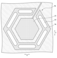
- FIG. 20 is a diagram showing a sixth variation of the pattern A.
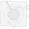
- Fig. 21 is a diagram showing a sixth variation of the pattern B.
- the first measurement electrode 21 and the second measurement electrode 22 have a rectangular shape when viewed in a plane.
- the first measurement electrode 21 and the second measurement electrode 22 have a hexagonal shape when viewed in a plane.
- the first measurement electrode 21 and the second measurement electrode 22 are circular in plan view, the area efficiency of the surface layer 12 of the resin substrate 10 may decrease. Therefore, the first measurement electrode 21 and the second measurement electrode 22 are polygonal, such as a hexagon, in plan view. Then, the number of vertices in the polygon is adjusted. This makes it possible to achieve a high level of balance between the detection power when measuring the dielectric constant and the area efficiency of the surface layer 12 of the resin substrate 10.
- the 20 and 21 show an example in which the shape of the first measurement electrode 21 and the second measurement electrode 22 in a plan view is hexagonal.
- the shape of the polygon is not limited to a hexagon.
- the polygon can be an N-sided polygon.
- the number of vertices N can be a natural number equal to or greater than 3.
- the first cutout 51 and the second cutout 52 are formed by arranging six long holes along the outer edge of the first measurement electrode 21 or the second measurement electrode 22.
- the six long holes are arranged in a hexagonal ring shape along the outer edge of the first measurement electrode 21 and the second measurement electrode 22.
- first cut hole 51 and the second cut hole 52 are not limited to elongated holes.
- the first cut hole 51 and the second cut hole 52 may be round holes, or a combination of round holes and elongated holes may be used.
- the shape of the surface moisture-proof layer 74 in pattern A in plan view is a hexagonal ring shape that corresponds to the arrangement of the first cutouts 51.
- the surface moisture-proof layer 74 has a shape in which copper foil is molded into a hexagonal ring shape.
- (Appendix 1) a measurement electrode pair including two measurement electrodes arranged to sandwich at least a portion of the resin substrate (10);
- the resin base material has a through hole penetrating in a thickness direction of the resin base material, the through hole is disposed at least partially around the measurement electrode in a plan view,
- the measurement electrode pair includes a first measurement electrode pair (7) and a second measurement electrode pair (9),
- the measurement electrode included in the first measurement electrode pair (7) is a first measurement electrode (21)
- the measurement electrode included in the second measurement electrode pair (9) is a second measurement electrode (22)
- a moisture-proof layer (70) is formed on the side surface of the through hole arranged around the first measuring electrode (21)
- the resin substrate (10) is exposed from a side surface of the through hole arranged around the second measurement electrode (22).
- Wiring board (1) (1).
- the measuring electrode and the moisture-proof layer (70) are copper foil, The first measuring electrode (21) is not in contact with the moisture-proof layer (70).
- At least one of the two first measurement electrodes (21) included in the first measurement electrode pair (7) and at least one of the two second measurement electrodes (22) included in the second measurement electrode pair (9) are disposed inside the resin substrate (10).
Landscapes
- Engineering & Computer Science (AREA)
- Microelectronics & Electronic Packaging (AREA)
- General Engineering & Computer Science (AREA)
- Physics & Mathematics (AREA)
- General Physics & Mathematics (AREA)
- Manufacturing & Machinery (AREA)
- Investigating Or Analyzing Materials By The Use Of Electric Means (AREA)
Abstract
配線基板は、樹脂基材の少なくとも一部を挟んで配置された2つの測定用電極を含む測定用電極対と、前記樹脂基材を、前記樹脂基材の厚さ方向に貫通する貫通穴と、を備え、前記貫通穴は、平面視において前記測定用電極の周りの少なくとも一部に配置され、前記測定用電極対は、第1の測定用電極対と、第2の測定用電極対とを含み、前記第1の測定用電極対に含まれる前記測定用電極を第1の測定用電極とし、前記第2の測定用電極対に含まれる前記測定用電極を第2の測定用電極としたとき、前記第1の測定用電極の周りに配置された前記貫通穴の側面には、防湿層が形成され、前記第2の測定用電極の周りに配置された前記貫通穴の側面からは、前記樹脂基材が露出する。
Description
本開示は、配線基板に関する。
プリント配線基板などの配線基板は、通常、(吸水性を有する)樹脂基材を含む。そのため、配線基板は、水分を吸収する。配線基板が水分を吸収すると、配線基板の誘電率が変化する。誘電率の変化は、インピーダンスの変化を招く。配線基板のインピーダンスが変化すると、配線基板が用いられる回路に動作不良などが発生する。
配線基板の動作不良の検知に関する技術が知られている(例えば、特許文献1参照)。この技術では、例えば、異常を事前に検知するための配線が、配線基板に形成される。
ところで、配線基板に形成された回路で扱われる信号が高速化し、または高周波化すると、より厳格なインピーダンスマッチングが、配線基板に求められる。そのため、配線基板の的確な予防および保全が求められる。
配線基板の予防とは、配線基板のインピーダンスの変化量が許容範囲を超えることを予防することをいう。配線基板の予防の例は、インピーダンスが変化した配線基板を回収し、正常なインピーダンスを有する配線基板に交換することである。
配線基板の保全とは、インピーダンスが許容範囲内で変化した配線基板について、インピーダンスがそれ以上変化しないようにすることをいう。
配線基板の予防および保全は、配線基板が製品に組み込まれ、製品が出荷された以降に、特に求められる。出荷された製品が置かれる環境はさまざまであり、また、製品は、長期にわたって使用されるからである。
そこで、本開示は、配線基板が組み込まれた製品が出荷された以降においても、的確な予防および保全ができる配線基板を提供することを目的とする。
本開示の配線基板は、樹脂基材の少なくとも一部を挟んで配置された2つの測定用電極を含む測定用電極対と、前記樹脂基材を、前記樹脂基材の厚さ方向に貫通する貫通穴と、を備え、前記貫通穴は、平面視において前記測定用電極の周りの少なくとも一部に配置され、前記測定用電極対は、第1の測定用電極対と、第2の測定用電極対とを含み、前記第1の測定用電極対に含まれる前記測定用電極を第1の測定用電極とし、前記第2の測定用電極対に含まれる前記測定用電極を第2の測定用電極としたとき、
前記第1の測定用電極の周りに配置された前記貫通穴の側面には、防湿層が形成され、前記第2の測定用電極の周りに配置された前記貫通穴の側面からは、前記樹脂基材が露出する。
前記第1の測定用電極の周りに配置された前記貫通穴の側面には、防湿層が形成され、前記第2の測定用電極の周りに配置された前記貫通穴の側面からは、前記樹脂基材が露出する。
本開示の配線基板によれば、配線基板が組み込まれた製品が出荷された以降においても、的確な予防および保全ができる配線基板を提供することができる。
本開示を実施するための形態を、図1から図4を参照して説明する。図1および図2は、配線基板1を平面視した図である。図3および図4は、配線基板1の斜視図である。図3は、図1の100-100線断面を示す。図4は、図2の102-102線断面を示す。
図に、XYZ直交座標系を示す。X方向、Y方向、およびZ方向が示す方向は、各図において同じである。Z方向は、配線基板1の厚さ方向である。X方向は、後に説明する測定用電極の外周辺に直線状に延びる辺がある場合、その辺と平行な方向である。例えば、図1に、測定用電極の一例である第1の測定用電極21を示す。第1の測定用電極21は、直線状に延びる外周辺211を有する。そこで、外周辺211が延びる方向と平行な方向をX方向とする。
図1および図2は、配線基板1のXY平面に平行な表面を示す。図3および図4は、配線基板1のXZ平面に平行な断面を示す。配線基板1をZ方向からみることを、平面視と呼ぶ。
配線基板1は、樹脂基材10および導電体を含む。樹脂基材10は、樹脂で形成された基板である。樹脂基材10は、絶縁層として機能する。
導電体は、樹脂基材10の表面などに配置される導体である。導電体は、種々の形態で樹脂基材10に配置される。形態の例は、電極、配線および貫通穴めっきなどである。導電体は、銅はく(銅箔)などで形成される。
導電体は、少なくとも2種類の導電体配置のパターンで配線基板1に配置される。1つのパターンをパターンAと呼ぶ。もう1つのパターンをパターンBと呼ぶ。パターンAは、樹脂基材10の吸湿を阻害するパターンである。パターンBは、樹脂基材10の吸湿を促進するパターンである。
図1および図3は、パターンAの導電体配置を示す。図2および図4は、パターンBの導電体配置を示す。
パターンAの導電体配置、およびパターンBの導電体配置は、いずれも、測定用電極対および貫通穴、すなわち切り穴を含む。測定用電極対は、樹脂基材10を挟んで対面するように配置される2つの測定用電極を含む。測定用電極は、銅はくで形成される。この2つの測定用電極が電極対を構成する。パターンAに含まれる測定用電極対を、第1の測定用電極対7と呼ぶ。パターンBに含まれる測定用電極対を、第2の測定用電極対9と呼ぶ。
第1の測定用電極対7が含む2つの測定用電極を、第1の測定用電極21と呼ぶ。第2の測定用電極対9が含む2つの測定用電極を、第2の測定用電極22と呼ぶ。
切り穴は、樹脂基材10を貫通する貫通穴である。切り穴は、樹脂基材10の厚さ方向Zに樹脂基材10を貫通する。パターンAに含まれる切り穴を、第1の切り穴51と呼ぶ。パターンBに含まれる切り穴を、第2の切り穴52と呼ぶ。
パターンAとパターンBとは、切り穴に防湿層70が設けられるか否かが異なる。
切り穴に防湿層70が設けられていない場合、切り穴の側面からは樹脂基材10が露出する。樹脂基材10は、吸湿しやすい。
防湿層70は、樹脂基材10が切り穴から吸湿することを抑制する層である。防湿層70は、切り穴の側面、および樹脂基材10の表層における切り穴の周囲に形成される。防湿層70については、後に具体的に説明する。防湿層70は、銅はくなどによって形成される。銅はくは、水分の通過を抑制する。銅はくは、めっきなどによって形成できる。
切り穴に防湿層70が設けられていない場合には、切り穴は、切り穴が設けられていない樹脂基材と比べて、樹脂基材10の吸湿を促進する。切り穴に防湿層70が設けられている場合には、防湿層70は、樹脂基材10の吸湿を阻害する。
パターンAの第1の切り穴51には、防湿層70が設けられる。パターンAは、吸湿阻害パターンとして機能する。パターンBの第2の切り穴52には、防湿層70は設けられない。パターンBは、吸湿促進パターンとして機能する。
(パターンA)
図1および図3に基づいて、パターンAを具体的に説明する。図3に示すように、パターンAは、第1の測定用電極対7を含む。第1の測定用電極対7は、2つの第1の測定用電極21を含む。2つの第1の測定用電極21は、樹脂基材10を挟んで対面するように配置される。
図1および図3に基づいて、パターンAを具体的に説明する。図3に示すように、パターンAは、第1の測定用電極対7を含む。第1の測定用電極対7は、2つの第1の測定用電極21を含む。2つの第1の測定用電極21は、樹脂基材10を挟んで対面するように配置される。
図1に示すように、第1の測定用電極21の形状は、平面視において四角形状(矩形状)である。第1の測定用電極21の4辺の近傍には、第1の切り穴51が形成される。第1の切り穴51は、第1の測定用電極21の4辺のそれぞれ対して、その近傍に、形成される。第1の切り穴51は、X方向またはY方向に延びる。
図3に示すように、第1の切り穴51は、樹脂基材10に形成された貫通穴である。第1の切り穴51は、樹脂基材10が、樹脂基材10の厚さ方向に取り除かれて形成された穴である。樹脂基材10の厚さ方向は、Z方向である。図1に示すように、第1の切り穴51の形状は、平面視において、長穴形状である。長穴形状における長手方向は、第1の測定用電極21の外辺が延びる方向と平行である。
第1の切り穴51には、防湿層70が形成される。防湿層70は、銅はくで形成される。防湿層70は、側面防湿層72および表層防湿層74を含む。図3に示すように、側面防湿層72は、第1の切り穴51の側面54に形成される防湿層70である。第1の切り穴51の側面54は、樹脂基材10に形成された貫通穴の内壁面である。
図1および図3に示すように、表層防湿層74は、樹脂基材10の表層12に形成される防湿層70である。
側面防湿層72は、第1の切り穴51の側面54の全面を覆うように形成される。側面防湿層72が側面54の全面を覆うことによって、樹脂基材10が側面54を介して吸湿することを抑制できる。
表層防湿層74は、平面視において、第1の切り穴51の周囲を覆うように配置される。
側面防湿層72と表層防湿層74とは、連続する。側面防湿層72と表層防湿層74とが連続するとは、側面防湿層72と表層防湿層74との間から樹脂基材10が露出しないことをいう。側面防湿層72と表層防湿層74とが連続することによって、樹脂基材10の吸湿をより抑制できる。
図1に示すように、表層防湿層74は、平面視において、第1の切り穴51を取り囲むように形成される。そのため、表層防湿層74の形状は、平面視において、輪状である。
表層防湿層74と第1の測定用電極21との間には、隙間104がある。隙間104は、X方向またはY方向に延びる。隙間104は、導電体が形成されていない部分である。表層防湿層74は、第1の測定用電極21と導通しない。なお、後に説明する隙間106および隙間108も、隙間104と同様に、導電体が形成されていない部分である。
図1に示す例では、第1の切り穴51は、4つ形成される。表層防湿層74は、4つの第1の切り穴51のそれぞれに形成される。そのため、表層防湿層74は、第1の測定用電極21の外辺に沿って、4つ形成される。ここで、隣り合う表層防湿層74の間には、隙間106がある。隙間106によって、隣り合う表層防湿層74は、導通しない。
樹脂基材10の表層12には、測定用引き出し配線40が形成される。測定用引き出し配線40は、第1の測定用電極対7の静電容量を測定する際に用いられる接続用の配線である。測定用引き出し配線40は、その1つの端において、第1の測定用電極21に接続される。表層防湿層74と測定用引き出し配線40との間には、隙間108がある。隙間108によって、表層防湿層74は、第1の測定用電極21と導通しない。
(パターンB)
図2および図4に基づいて、パターンBを説明する。パターンBについては、パターンAとの相違点を中心に説明する。説明しない点については、パターンAの説明が援用される。パターンBは、防湿層70が形成されていない点以外は、パターンAと同様である。
図2および図4に基づいて、パターンBを説明する。パターンBについては、パターンAとの相違点を中心に説明する。説明しない点については、パターンAの説明が援用される。パターンBは、防湿層70が形成されていない点以外は、パターンAと同様である。
図4に示すように、パターンBは、第2の測定用電極対9を含む。第2の測定用電極対9は、2つの第2の測定用電極22を含む。2つの第2の測定用電極22は、樹脂基材10を挟んで対面するように配置される。
第2の測定用電極22の形状は、平面視において四角形状(矩形状)である。第2の測定用電極22の4辺の近傍には、第2の切り穴52が形成される。
パターンBが含む第2の測定用電極対9の形状は、パターンAが含む第1の測定用電極対7の形状と、同じである。また、パターンBが含む第2の切り穴52の形状は、パターンAが含む第1の切り穴51の形状と同じである。
第2の切り穴52には、防湿層70が形成されない。そのため、図4に示すように、第2の切り穴52の側面54からは、樹脂基材10が露出する。
上述のように、パターンAとパターンBとは、防湿層70の有無が異なる。パターンAでは、防湿層70が形成される。そのため、図3に矢印110に示す、切り穴の側面54からの樹脂基材10の吸湿は、阻害される。パターンAは、吸湿を阻害する導電体配置である。
一方、パターンBでは、防湿層70は形成されない。そのため、図4に矢印112に示すように、樹脂基材10は切り穴の側面54から吸湿する。切り穴の側面54からの吸湿が加わることによって、配線基板1の吸湿は、促進される。パターンBは、吸湿を促進する導電体配置である。
吸湿阻害のパターンであるパターンAを基準として、吸湿促進のパターンであるパターンBとの誘電率の差分を測定する。これによって、吸湿による誘電率の変化を確認できる。誘電率の変化を確認することによって、樹脂基材10の吸湿の程度を把握できる。インピーダンスは、誘電率から間接的に測定できる。
図5は、配線基板1の各部の長さと、配線基板1のインピーダンスZ0との関係を示す図である。Wは、樹脂基材10の表層12に形成された測定用モデル電極32のX方向の長さである。tは、測定用モデル電極32のZ方向の長さである。tは、測定用モデル電極32の厚さに等しい。hは、樹脂基材10のZ方向の長さである。hは、樹脂基材10の厚さに等しい。
樹脂基材10における表層12と対向する面には、対向電極30が形成される。対向電極30は、樹脂基材10を挟んで測定用モデル電極32と対面する。測定用モデル電極32と対向電極30との距離は、上述したhである。
εrは、樹脂基材10の比誘電率である。配線基板1が吸湿した場合であっても、樹脂基材10の厚さh、測定用モデル電極32のX方向の長さW、および測定用モデル電極32の厚さtは変化しない。そのため、図5の式120に示すように、樹脂基材10の比誘電率εrと、配線基板1のインピーダンスZ0とは相関する。
図6に基づいて、樹脂基材10の誘電率の測定方法を説明する。図6は、配線基板1の各部の長さと、樹脂基材10の誘電率εとの関係を示す図である。樹脂基材10の誘電率εは、配線基板1に形成された測定用電極対を用いて測定できる。具体的には、パターンAでは第1の測定用電極対7を用いて、またパターンBでは第2の測定用電極対9を用いて、樹脂基材10の誘電率εを測定できる。樹脂基材10の誘電率εを測定することによって、図5の式120を用いて、配線基板1のインピーダンスZ0を算出できる。
図6に示す測定用モデル電極対34が含む2つの測定用電極を、測定用モデル電極36とする。2つの測定用モデル電極36は、樹脂基材10を挟んで対面するように配置される。測定用モデル電極36には、配線37が接続される。図6に示すSは、測定用モデル電極36の面積である。dは、樹脂基材10のZ方向の長さである。dは、樹脂基材10の厚さに等しい。また、dは、2つの測定用モデル電極36の距離である。Cは、樹脂基材10の静電容量である。εは、樹脂基材10の誘電率である。配線基板1に形成された測定用モデル電極対34は、コンデンサと等価である。そこで、配線37を介して測定用モデル電極対34を充電し、2つの測定用モデル電極36間の電位差を測定することによって、樹脂基材10の静電容量Cを測定する。そして、図6の式122に基づいて、樹脂基材10の誘電率εを求める。
樹脂基材10の誘電率εが求まると、図5の式120によって、配線基板1のインピーダンスZ0を求めることができる。
図7に基づいて、配線基板1を用いた、配線基板1の予防および保全を説明する。図7は、導電体配置パターンごとの、各流通段階における誘電率を示す図である。図7では、流通段階として、配線基板製造時点、ユニット製造メーカ納入時点、およびフィールドの3つの段階を示す。フィールドとは、ユニットが出荷された市場をいう。
配線基板1は、1つの配線基板内に、吸湿阻害パターンであるパターンAの導電体配置と、吸湿促進パターンであるパターンBの導電体配置とを含む。そのため、吸湿阻害のパターンAを基準として、吸湿促進のパターンBとの誘電率の差分を測定することによって、吸湿による誘電率の変化を確認することができる。
また、吸湿促進のパターンBは、配線基板1内で機能している個所より速く吸湿する構造を有する。すなわち、パターンBは、樹脂基材10に貫通穴が開けられることによって、樹脂基材10が空気と直接触れる面積が増え、樹脂基材10が吸湿しやすい構造を有する。これにより、予防および保全としてアラートを上げやすい構造を実現することができる。すなわち、吸湿による配線基板1の状態変化を、早期に、的確に確認することができる。
図7に基づいて、吸湿による配線基板1の状態変化の例を説明する。図7に示す例では、配線基板1が製造された時点において、パターンAの樹脂基材10の誘電率は、3.8である。パターンBの樹脂基材10の誘電率も、3.8である。配線基板1が製造された時点では、パターンAとパターンBとで、樹脂基材10の吸湿の程度に差はないと考えられる。
その後、配線基板1は、ユニット製造メーカに輸送される。配線基板1がユニット製造メーカに納入された時点で、パターンAの樹脂基材10の誘電率は、3.8である。パターンBの樹脂基材10の誘電率は、4.0である。パターンAの樹脂基材10の誘電率は、配線基板製造時点から変化していない。一方、パターンBの樹脂基材10の誘電率は、配線基板製造時点から0.2上昇している。パターンAは、吸湿阻害パターンであるため、樹脂基材10は吸湿しない。パターンBは、吸湿促進パターンであるため、樹脂基材10は吸湿する。
パターンAでは、樹脂基材10が吸湿しないため、誘電率は変化しないと考えられる。パターンBでは、樹脂基材10が吸湿するため、誘電率が上昇すると考えられる。
その後、配線基板1は、出荷され、フィールドに出る。フィールドにおいて、パターンAの樹脂基材10の誘電率は、3.8である。パターンBの樹脂基材10の誘電率は、4.2である。パターンAの樹脂基材10の誘電率は、配線基板製造時点から変化していない。パターンAは、吸湿阻害パターンであるため、樹脂基材10が吸湿しないためであると考えられる。一方、パターンBの樹脂基材10の誘電率は、4.2である。パターンBの樹脂基材10の誘電率は、ユニット製造メーカ納入時点から、さらに0.2上昇している。パターンBでは、樹脂基材10の吸湿が、さらに進んだものと考えられる。
上述のように、パターンAの誘電率は、配線基板製造時点から、フィールドに至るまで、変化しない。そのため、配線基板製造時点の誘電率が不明であっても、各時点において、パターンBの誘電率のパターンAの誘電率に対する差を評価することによって、樹脂基材10の吸湿の状態を確認することができる。
従来例との相違を説明する。図8は、従来の配線基板200における誘電率の変化の例を示す図である。従来の配線基板200では、1枚の配線基板200の中に、吸湿促進パターンと、吸湿促進パターンと対比するための吸湿阻害パターンとの、2つのパターンの導電体配置は形成されていない。そのため、配線基板200から、吸湿の状態を確認するための、基準となる値を求めることはできない。
樹脂基材の吸湿の状態を確認するためには、図8に矢印130で示す、配線基板製造時点での配線基板200の誘電率を把握する必要がある。配線基板製造時点より後で、吸湿していない樹脂基材10の誘電率を測定できないからである。
しかし、通常、ユニット製造メーカは、配線基板製造時点での配線基板200の誘電率を把握できない。ユニット製造メーカが配線基板200の誘電率を測定できる期間は、例えば、図8に矢印132で示す期間のようになる。すなわち、ユニット製造メーカは、配線基板200が納入された時点から、配線基板200を保管し、配線基板200を用いてユニットを製造し、ユニットを出荷する時点までの間は、誘電率を測定できる。しかし、図8に矢印130で示す配線基板製造時点のおける誘電率は測定できない。
そのため、従来の配線基板200では、樹脂基材の吸湿の状態を正確に確認することは困難である。例えば、出荷時点での誘電率が4.3であった場合、その値が、樹脂基材の吸湿の観点から問題とすべき値であるか否かを正確に判断することは困難である。樹脂基材の吸湿の状態を正確に判断するためには、吸湿していない状態での樹脂基材の誘電率が必要だからである。
これに対して本実施形態の配線基板1では、いずれの時点においても、基準となる値に基づいて、樹脂基材10の吸湿の状態を正確に確認できる。配線基板1が、吸湿阻害のパターンAを含むためである。そのため、例えば、パターンBの誘電率と、パターンAの誘電率との差異が大きくなったとき、すなわち、パターンBの誘電率の上昇が大きくなったときに、樹脂基材10の吸湿が大きくなったと判断して、アラートを出すことができる。
以上、配線基板1の一構成例として、第1の測定用電極21および第2の測定用電極22の平面視における形状が四角形状である場合を説明した。また、切り穴の平面視における形状が長穴である場合を説明した。測定用電極および切り穴の形状は、これには限定されない。以下、測定用電極および切り穴の変形例を説明する。
(変形例1)
図9および図10に基づいて、導電体配置の変形例1を説明する。図9は、パターンAの変形例1を示す図である。図10は、パターンBの変形例1を示す図である。以下、各変形例の説明では、図1から図4に基づいて説明した導電体配置と異なる点を中心に説明する。
図9および図10に基づいて、導電体配置の変形例1を説明する。図9は、パターンAの変形例1を示す図である。図10は、パターンBの変形例1を示す図である。以下、各変形例の説明では、図1から図4に基づいて説明した導電体配置と異なる点を中心に説明する。
以下、図1から図4に基づいて説明した導電体配置を、基本例と呼ぶ。また、第1の切り穴51および第2の切り穴52を、単に、切り穴と呼ぶ。第1の切り穴51の形状および第2の切り穴52の形状を、単に、切り穴の形状と呼ぶ。
基本例では、切り穴の形状は、平面視において、長穴形状であった。これに対して、変形例1では、図9および図10に示すように、切り穴の形状は、平面視において、丸穴形状である。
切り穴の形状を長穴形状にすることによって、レジンリセッションおよび導電体の剥離を抑制できる。導電体の剥離とは、ランド、パッド、および電極などの剥離をいう。
図9および図10に示す例では、基本例の切り穴1つに代わって、丸穴が4つまたは5つ形成される。この丸穴の数は例示である。図1の切り穴1つに代わって形成する丸穴の数は、任意である。また、丸穴の配置は、直線状の1列に限定されない。丸穴の配置は、例えば2列以上にすることができる。
(変形例2)
図11および図12に基づいて、導電体配置の変形例2を説明する。図11は、パターンAの変形例2を示す図である。図12は、パターンBの変形例2を示す図である。
図11および図12に基づいて、導電体配置の変形例2を説明する。図11は、パターンAの変形例2を示す図である。図12は、パターンBの変形例2を示す図である。
基本例では、切り穴を構成する長穴は、第1の測定用電極21の各外辺、および第2の測定用電極22の各外辺の近傍に、1つずつ形成されていた。これに対して、変形例2では、長穴は、外辺毎に、各外辺の近傍に2つ形成される。そのため、変形例2の長穴の長辺の長さは、基本例の長穴の長辺の長さよりも短い。
切り穴を長穴で形成する場合、長穴の長辺の長さが長くなると、不良が発生しやすくなる場合がある。また、配線基板製造上の制約から、長穴の最大長さには制限がある。
そこで、変形例2では、基本例の長穴1つに代わって、長穴を2つ形成する。これによって、切り穴の必要な大きさを確保しながら、1つの長穴の長辺の長さが長くなり過ぎないようにできる。
なお、図11および図12に示す例では、基本例の長穴1つに代わって、長穴が2つ形成される。この長穴の数は例示である。基本例の長穴1つに代わって形成する小さい長穴の数は2つ以上の任意の数に設定できる。
また、形成する長穴の大きさは、均一でなくてもよい。例えば、図11に示す長穴56と長穴57のように、長辺の長さが異なる長穴を形成してもよい。
(変形例3)
図13および図14に基づいて、導電体配置の変形例3を説明する。図13は、パターンAの変形例3を示す図である。図14は、パターンBの変形例3を示す図である。
図13および図14に基づいて、導電体配置の変形例3を説明する。図13は、パターンAの変形例3を示す図である。図14は、パターンBの変形例3を示す図である。
基本例では、切り穴は、長穴のみで形成されていた。これに対して、変形例3では、切り穴は、長穴および丸穴で形成される。切り穴を、長穴および丸穴で形成することによって、第1の測定用電極21および第2の測定用電極22の各外辺の近傍において、各外辺の長さに対して切り穴が形成されている長さの割合を大きくすることが容易になる。その結果、パターンAにおいて、吸湿阻害の性能を高くできる。また、パターンBにおいて、吸湿促進の性能を高くできる。
長穴は、通常、丸穴を複数回ドリリングすることによって形成される。複数回のドリリングにおいて、位置ずれが発生する場合がある。また、複数回のドリリングに耐えるために、長穴が形成される部分の周囲の樹脂基材10は、十分な剛性を有することが好ましい。
以上の理由から、長穴と他の切り穴との間の設計上の距離、および長穴と測定用電極との間の設計上の距離などは、丸穴の場合よりも、長いことが好ましい。言い換えると、長穴の周りには、長穴の位置ずれを許容することができ、また、ドリリングの際に支えとなりうる十分な剛性を確保できるような面積の樹脂基材10があることが好ましい。この穴の周りで支えなどになる部分は、残り代と呼ばれる。残り代には、通常、切り穴は形成されない。
ここで、長穴を形成してから丸穴を開けることによって、切り穴を形成し終えた際に残る残り代を小さくできる。長穴を形成する際の残り代に、長穴を形成した後に丸穴を形成する。丸穴を形成する際には、周りの樹脂基材10に、長穴を形成する際ほど、剛性は必要とされない。そのため、丸穴における残り代は、長穴における残り代よりも小さくてもよい。
以上のように、長穴を形成した後、長穴に対する残り代に丸穴を形成することによって、切り穴を形成した後に残る残り代を小さくすることができる。前述のように、残り代は、切り穴が形成されない部分である。残り代が小さいことは、第1の測定用電極21および第2の測定用電極22の各外辺の近傍に、切り穴がより長く形成されることを意味する。
第1の測定用電極21の各外辺の近傍に形成される第1の切り穴51には、防湿層70が形成される。残り代が小さくなると、パターンAでは、平面視において第1の測定用電極対7の周辺により多くの防湿層70が配置される。すなわち、平面視において第1の測定用電極対7の周辺がより長い距離にわたって防湿層70に覆われる。その結果、パターンAにおいて、銅はくなどによる密閉空間の質を高め、吸湿阻害の性能を高めることができる。
第2の測定用電極22の各外辺の近傍に形成される第2の切り穴52の側面からは樹脂基材10が露出する。残り代が小さくなると、パターンBでは、平面視において第2の測定用電極対9の周辺により多く樹脂基材10が露出する。その結果、パターンBにおいて、吸湿促進の性能を高くできる。
図13および図14には、基本例の長穴1つに代わって、1つの長穴56および1つの丸穴57を形成する例、ならびに、1つの長穴56および2つの丸穴57を形成する例を示した。ただし、長穴と丸穴とは、様々な組み合わせによる配置が可能である。例えば、丸穴の数を増やすこと、および長穴と丸穴との配列の順番を変更すること、などができる。
(変形例4)
図15に基づいて、導電体配置の変形例4を説明する。図15は、パターンAの変形例4を示す図である。図16は、基本例のパターンAを示す図である。図15および図16は、いずれも、配線基板1のXZ断面図である。
図15に基づいて、導電体配置の変形例4を説明する。図15は、パターンAの変形例4を示す図である。図16は、基本例のパターンAを示す図である。図15および図16は、いずれも、配線基板1のXZ断面図である。
変形例4と基本例とでは、第1の測定用電極21が配置されている位置が異なる。基本例では、図16に示すように、2つの第1の測定用電極21は、樹脂基材10のZ方向における両方の表層12に配置される。これに対して、変形例4では、図15に示すように、1つの第1の測定用電極21は、樹脂基材10のZ方向における表層12に配置され、もう1つの第1の測定用電極21は、樹脂基材10の内部に配置される。具体的には、図15に示すように、2つの第1の測定用電極21のうち、1つの第1の測定用電極211は、樹脂基材10の表層12ではなく、樹脂基材10の内部に配置される。
変形例4では、配線基板1における、デッドスペースを少なくすることができる。デッドスペースとは、部品などが実装できない部分をいう。樹脂基材10の表層12に第1の測定用電極21が配置される場合、その部分には、部品を実装することができない。その部分はデッドスペースとなる。図15および図16において、矢印114で示す部分がデッドスペースである。基本例では、図16に示すように、樹脂基材10の両面にデッドスペースがある。これに対して、変形例4では、樹脂基材10の1つの面のみにデッドスペースがある。1つの第1の測定用電極21が、樹脂基材10の内部に配置されるからである。
図15に示すように、1つの第1の測定用電極21を樹脂基材10の内部に配置することでデッドスペースではなくなった部分に、部品60を実装できる。図15に示す例では、樹脂基材10に導電体でパッド62を形成する。そのパッド62に、部品60を実装する。
図15に示すように、1つの第1の測定用電極21を樹脂基材10の内部に配置することによって、部品を実装できる領域を増やすことができる。
また、1つの第1の測定用電極21を樹脂基材10の内部に配置することによって、誘電率の変化の検出力が高くなる。1つの第1の測定用電極21を樹脂基材10の内部に配置することによって、2つの第1の測定用電極21の距離が短くなる。2つの第1の測定用電極21の距離が短くなると、誘電率の小さな変化を検出することが可能になるためである。
なお、図15に示す構成は例示である。2つの第1の測定用電極21のそれぞれについて、樹脂基材10の表層12に配置する、または樹脂基材10の内部に配置するなど、種々の変形が可能である。
また、パターンBについても、パターンAと同様の変形が可能である。
測定用電極を樹脂基材10の内部に配置する場合であっても、測定用電極を樹脂基材10の表層12に配置する場合と同様に、樹脂基材10の比誘電率εrに基づいて、配線基板1のインピーダンスZ0を求めることができる。図17は、測定用モデル電極32が、樹脂基材10の内部に位置する場合の、配線基板1の各部の長さとインピーダンスとの関係を示す図である。図17に記載された符号などの意味は、図5と同じである。測定用モデル電極32が、樹脂基材10の内部に配置される場合は、図5に示す式120にかわり、図17に示す式124を用いて、配線基板1のインピーダンスZ0を求めることができる。
(変形例5)
図18よび図19に基づいて、導電体配置の変形例5を説明する。図18は、パターンAの変形例5を示す図である。図19は、パターンBの変形例5を示す図である。
図18よび図19に基づいて、導電体配置の変形例5を説明する。図18は、パターンAの変形例5を示す図である。図19は、パターンBの変形例5を示す図である。
基本例では、第1の測定用電極21および第2の測定用電極22は、四角形の銅はくで形成されていた。これに対して、変形例5では、第1の測定用電極21および第2の測定用電極22は、円形の銅はくで形成される。
これによって、樹脂基材10の比誘電率εr、ひいては配線基板1のインピーダンスZ0について、より安定した測定結果を得ることができる。第1の測定用電極21および第2の測定用電極22の形状が四角形の場合、銅はくの形状も四角形になる。この場合、四角形の角に当たる部分の銅はくの形成ばらつきによって、測定値にばらつきが生じる場合がある。これに対して、第1の測定用電極21および第2の測定用電極22の形状が円形である場合には、銅はくの形状も円形になる。銅はくが円形の場合、第1の測定用電極21および第2の測定用電極22の形状は点対称となる。そのため、第1の測定用電極21および第2の測定用電極22の形状が四角形である場合比べて、測定結果が安定する。
第1の測定用電極21および第2の測定用電極22の形状が円形であることによって、第1の切り穴51および第2の切り穴52は、輪状に配置される。図18および図19に示す例では、第1の切り穴51および第2の切り穴52は、複数個の丸穴によって形成される。そして、複数個の丸穴が、輪状に配列される。
なお、変形例5において、第1の切り穴51および第2の切り穴52は、丸穴に限定されない。第1の切り穴51および第2の切り穴52は、長穴でもよく、または、丸穴と長穴とを併用してもよい。
パターンAにおける表層防湿層74の平面視における形状は、第1の切り穴51の配置に対応して、輪状である。表層防湿層74は、銅はくが、輪状に成型された形状を有する。
(変形例6)
図20よび図21に基づいて、導電体配置の変形例6を説明する。図20は、パターンAの変形例6を示す図である。図21は、パターンBの変形例6を示す図である。
図20よび図21に基づいて、導電体配置の変形例6を説明する。図20は、パターンAの変形例6を示す図である。図21は、パターンBの変形例6を示す図である。
基本例では、第1の測定用電極21および第2の測定用電極22の平面視における形状は、四角形状であった。これに対して、変形例6では、第1の測定用電極21および第2の測定用電極22の平面視における形状は、六角形状である。
これによって、誘電率測定の際の検出力と、樹脂基材10の表層12の面積効率とをバランスさせることができる。第1の測定用電極21および第2の測定用電極22は、その面積が大きいほど誘電率測定の検出力が高い。誘電率の小さな変化を増幅できるからである。
第1の測定用電極21および第2の測定用電極22の平面視での形状を円形状にした場合、樹脂基材10の表層12の面積効率が低下する場合がある。そこで、第1の測定用電極21および第2の測定用電極22の平面視での形状を、六角形などの多角形とする。そして、多角形における、頂点の数を調整する。これによって、誘電率測定の際の検出力と、樹脂基材10の表層12の面積効率とを、高いレベルでバランスさせることができる。
なお、図20および図21では、第1の測定用電極21および第2の測定用電極22の平面視での形状が六角形である場合を例示した。ただし、多角形の形状は、六角形に限定されない。多角形は、N角形とすることができる。ここで、頂点数Nは3以上の自然数とすることができる。
第1の切り穴51および第2の切り穴52は、第1の測定用電極21または第2の測定用電極22の外辺に沿って6つの長穴が配置されることによって構成される。第1の測定用電極21および第2の測定用電極22の外辺に沿って、6つの長穴が、六角形状に輪状に配列される。
なお、第1の切り穴51および第2の切り穴52は、長穴に限定されない。第1の切り穴51および第2の切り穴52は、丸穴でもよく、または、丸穴と長穴とを併用してもよい。
また、パターンAにおける表層防湿層74の平面視における形状は、第1の切り穴51の配置に対応して、六角形状の輪状である。表層防湿層74は、銅はくが、六角形状に輪状に成型された形状を有する。
本開示について詳述したが、本開示は上述した個々の実施形態に限定されるものではない。これらの実施形態は、本開示の要旨を逸脱しない範囲で、または、特許請求の範囲に記載された内容とその均等物から導き出される本開示の趣旨を逸脱しない範囲で、種々の追加、置き換え、変更、部分的削除等が可能である。また、これらの実施形態は、組み合わせて実施することもできる。例えば、上述した実施形態において、各動作の順序や各処理の順序は、一例として示したものであり、これらに限定されるものではない。また、上述した実施形態の説明に数値又は数式が用いられている場合も同様である。
上記実施形態及び変形例に関し、更に以下の付記を開示する。
(付記1)
樹脂基材(10)の少なくとも一部を挟んで配置された2つの測定用電極を含む測定用電極対と、
前記樹脂基材を、前記樹脂基材の厚さ方向に貫通する貫通穴と、を備え、
前記貫通穴は、平面視において前記測定用電極の周りの少なくとも一部に配置され、
前記測定用電極対は、第1の測定用電極対(7)と、第2の測定用電極対(9)とを含み、
前記第1の測定用電極対(7)に含まれる前記測定用電極を第1の測定用電極(21)とし、前記第2の測定用電極対(9)に含まれる前記測定用電極を第2の測定用電極(22)としたとき、
前記第1の測定用電極(21)の周りに配置された前記貫通穴の側面には、防湿層(70)が形成され、
前記第2の測定用電極(22)の周りに配置された前記貫通穴の側面からは、前記樹脂基材(10)が露出する、
配線基板(1)。
(付記1)
樹脂基材(10)の少なくとも一部を挟んで配置された2つの測定用電極を含む測定用電極対と、
前記樹脂基材を、前記樹脂基材の厚さ方向に貫通する貫通穴と、を備え、
前記貫通穴は、平面視において前記測定用電極の周りの少なくとも一部に配置され、
前記測定用電極対は、第1の測定用電極対(7)と、第2の測定用電極対(9)とを含み、
前記第1の測定用電極対(7)に含まれる前記測定用電極を第1の測定用電極(21)とし、前記第2の測定用電極対(9)に含まれる前記測定用電極を第2の測定用電極(22)としたとき、
前記第1の測定用電極(21)の周りに配置された前記貫通穴の側面には、防湿層(70)が形成され、
前記第2の測定用電極(22)の周りに配置された前記貫通穴の側面からは、前記樹脂基材(10)が露出する、
配線基板(1)。
(付記2)
前記測定用電極および前記防湿層(70)は、銅はくであり、
前記第1の測定用電極(21)は、前記防湿層(70)と接しない。
前記測定用電極および前記防湿層(70)は、銅はくであり、
前記第1の測定用電極(21)は、前記防湿層(70)と接しない。
(付記3)
前記第1の測定用電極対(7)に含まれる2つの前記第1の測定用電極(21)のうちの少なくとも一方、および前記第2の測定用電極対(9)に含まれる2つの前記第2の測定用電極(22)のうちの少なくとも一方は、前記樹脂基材(10)の内部に配置される。
前記第1の測定用電極対(7)に含まれる2つの前記第1の測定用電極(21)のうちの少なくとも一方、および前記第2の測定用電極対(9)に含まれる2つの前記第2の測定用電極(22)のうちの少なくとも一方は、前記樹脂基材(10)の内部に配置される。
1 配線基板
7 第1の測定用電極対
9 第2の測定用電極対
10 樹脂基材
21 第1の測定用電極
22 第2の測定用電極
70 防湿層
7 第1の測定用電極対
9 第2の測定用電極対
10 樹脂基材
21 第1の測定用電極
22 第2の測定用電極
70 防湿層
Claims (3)
- 樹脂基材の少なくとも一部を挟んで配置された2つの測定用電極を含む測定用電極対と、
前記樹脂基材を、前記樹脂基材の厚さ方向に貫通する貫通穴と、を備え、
前記貫通穴は、平面視において前記測定用電極の周りの少なくとも一部に配置され、
前記測定用電極対は、第1の測定用電極対と、第2の測定用電極対とを含み、
前記第1の測定用電極対に含まれる前記測定用電極を第1の測定用電極とし、前記第2の測定用電極対に含まれる前記測定用電極を第2の測定用電極としたとき、
前記第1の測定用電極の周りに配置された前記貫通穴の側面には、防湿層が形成され、
前記第2の測定用電極の周りに配置された前記貫通穴の側面からは、前記樹脂基材が露出する、
配線基板。 - 前記測定用電極および前記防湿層は、銅はくであり、
前記第1の測定用電極は、前記防湿層と接しない、
請求項1に記載の配線基板。 - 前記第1の測定用電極対に含まれる2つの前記第1の測定用電極のうちの少なくとも一方、および前記第2の測定用電極対に含まれる2つの前記第2の測定用電極のうちの少なくとも一方は、前記樹脂基材の内部に配置される、
請求項1または2に記載の配線基板。
Priority Applications (1)
| Application Number | Priority Date | Filing Date | Title |
|---|---|---|---|
| PCT/JP2023/025464 WO2025013174A1 (ja) | 2023-07-10 | 2023-07-10 | 配線基板 |
Applications Claiming Priority (1)
| Application Number | Priority Date | Filing Date | Title |
|---|---|---|---|
| PCT/JP2023/025464 WO2025013174A1 (ja) | 2023-07-10 | 2023-07-10 | 配線基板 |
Publications (1)
| Publication Number | Publication Date |
|---|---|
| WO2025013174A1 true WO2025013174A1 (ja) | 2025-01-16 |
Family
ID=94214824
Family Applications (1)
| Application Number | Title | Priority Date | Filing Date |
|---|---|---|---|
| PCT/JP2023/025464 Ceased WO2025013174A1 (ja) | 2023-07-10 | 2023-07-10 | 配線基板 |
Country Status (1)
| Country | Link |
|---|---|
| WO (1) | WO2025013174A1 (ja) |
Citations (4)
| Publication number | Priority date | Publication date | Assignee | Title |
|---|---|---|---|---|
| JP2001156449A (ja) * | 1999-11-24 | 2001-06-08 | Nec Corp | 多層印刷配線板の製造方法 |
| JP2010177583A (ja) * | 2009-01-30 | 2010-08-12 | Tdk Corp | 電子部品内蔵基板、その製造方法、及びその検査方法 |
| WO2022030320A1 (ja) * | 2020-08-03 | 2022-02-10 | ファナック株式会社 | 劣化検出用プリント基板 |
| JP2022173911A (ja) * | 2021-05-10 | 2022-11-22 | 河村電器産業株式会社 | プリント基板の劣化検出装置及び劣化検出方法 |
-
2023
- 2023-07-10 WO PCT/JP2023/025464 patent/WO2025013174A1/ja not_active Ceased
Patent Citations (4)
| Publication number | Priority date | Publication date | Assignee | Title |
|---|---|---|---|---|
| JP2001156449A (ja) * | 1999-11-24 | 2001-06-08 | Nec Corp | 多層印刷配線板の製造方法 |
| JP2010177583A (ja) * | 2009-01-30 | 2010-08-12 | Tdk Corp | 電子部品内蔵基板、その製造方法、及びその検査方法 |
| WO2022030320A1 (ja) * | 2020-08-03 | 2022-02-10 | ファナック株式会社 | 劣化検出用プリント基板 |
| JP2022173911A (ja) * | 2021-05-10 | 2022-11-22 | 河村電器産業株式会社 | プリント基板の劣化検出装置及び劣化検出方法 |
Similar Documents
| Publication | Publication Date | Title |
|---|---|---|
| US6391669B1 (en) | Embedded structures to provide electrical testing for via to via and interface layer alignment as well as for conductive interface electrical integrity in multilayer devices | |
| US20130257462A1 (en) | Package structure with conformal shielding and inspection method using the same | |
| US8675369B2 (en) | Module board | |
| KR20080041999A (ko) | 기판, 이를 이용한 반도체 장치, 반도체 장치의 검사방법및 반도체 장치의 제조방법 | |
| US8237055B2 (en) | Circuit board | |
| US20210392742A1 (en) | Embedded microstrip with open slot for high speed signal traces | |
| US20140293559A1 (en) | Wiring board | |
| CN103796417B (zh) | 电路板及其制作方法 | |
| WO2025013174A1 (ja) | 配線基板 | |
| JP2009152499A (ja) | プリント配線板およびプリント配線板のインピーダンス保証方法 | |
| CN210467597U (zh) | 一种多层陶瓷电容器 | |
| TW201524296A (zh) | 校正片結構 | |
| KR20120086942A (ko) | 연성인쇄회로기판 및 연성인쇄회로 기판의 불량 검출 방법 | |
| JP6763447B2 (ja) | 薄膜キャパシタ及び薄膜キャパシタが埋め込まれた多層回路基板 | |
| CN220173699U (zh) | 电路模块 | |
| JPH09205281A (ja) | 多層プリント配線板の内層回路パターンずれ検査方法 | |
| TWI488281B (zh) | 適形屏蔽封裝模組 | |
| JPH09275274A (ja) | 多層集合基板 | |
| US8520354B2 (en) | Multilayered board semiconductor device with BGA package | |
| JPH0548272A (ja) | プリント配線板 | |
| JP2740709B2 (ja) | 多層印刷配線板の積層ずれ検出方法 | |
| CN103426867B (zh) | 适形屏蔽封装模组 | |
| CN103219295B (zh) | 适形掩模封装结构及检测方法 | |
| TWI607220B (zh) | 晶片測試架構及其電路板 | |
| TWI499372B (zh) | 適形遮蔽封裝結構及檢測方法 |
Legal Events
| Date | Code | Title | Description |
|---|---|---|---|
| 121 | Ep: the epo has been informed by wipo that ep was designated in this application |
Ref document number: 23945054 Country of ref document: EP Kind code of ref document: A1 |
|
| NENP | Non-entry into the national phase |
Ref country code: DE |