WO2025009357A1 - フレキシブルプリント配線板の製造方法及びフレキシブルプリント配線板 - Google Patents
フレキシブルプリント配線板の製造方法及びフレキシブルプリント配線板 Download PDFInfo
- Publication number
- WO2025009357A1 WO2025009357A1 PCT/JP2024/021580 JP2024021580W WO2025009357A1 WO 2025009357 A1 WO2025009357 A1 WO 2025009357A1 JP 2024021580 W JP2024021580 W JP 2024021580W WO 2025009357 A1 WO2025009357 A1 WO 2025009357A1
- Authority
- WO
- WIPO (PCT)
- Prior art keywords
- plating
- plating layer
- layer
- printed wiring
- flexible printed
- Prior art date
- Legal status (The legal status is an assumption and is not a legal conclusion. Google has not performed a legal analysis and makes no representation as to the accuracy of the status listed.)
- Ceased
Links
Images


Classifications
-
- H—ELECTRICITY
- H05—ELECTRIC TECHNIQUES NOT OTHERWISE PROVIDED FOR
- H05K—PRINTED CIRCUITS; CASINGS OR CONSTRUCTIONAL DETAILS OF ELECTRIC APPARATUS; MANUFACTURE OF ASSEMBLAGES OF ELECTRICAL COMPONENTS
- H05K1/00—Printed circuits
- H05K1/02—Details
-
- H—ELECTRICITY
- H05—ELECTRIC TECHNIQUES NOT OTHERWISE PROVIDED FOR
- H05K—PRINTED CIRCUITS; CASINGS OR CONSTRUCTIONAL DETAILS OF ELECTRIC APPARATUS; MANUFACTURE OF ASSEMBLAGES OF ELECTRICAL COMPONENTS
- H05K1/00—Printed circuits
- H05K1/02—Details
- H05K1/11—Printed elements for providing electric connections to or between printed circuits
-
- H—ELECTRICITY
- H05—ELECTRIC TECHNIQUES NOT OTHERWISE PROVIDED FOR
- H05K—PRINTED CIRCUITS; CASINGS OR CONSTRUCTIONAL DETAILS OF ELECTRIC APPARATUS; MANUFACTURE OF ASSEMBLAGES OF ELECTRICAL COMPONENTS
- H05K1/00—Printed circuits
- H05K1/02—Details
- H05K1/11—Printed elements for providing electric connections to or between printed circuits
- H05K1/115—Via connections; Lands around holes or via connections
- H05K1/116—Lands, clearance holes or other lay-out details concerning the surrounding of a via
-
- H—ELECTRICITY
- H05—ELECTRIC TECHNIQUES NOT OTHERWISE PROVIDED FOR
- H05K—PRINTED CIRCUITS; CASINGS OR CONSTRUCTIONAL DETAILS OF ELECTRIC APPARATUS; MANUFACTURE OF ASSEMBLAGES OF ELECTRICAL COMPONENTS
- H05K3/00—Apparatus or processes for manufacturing printed circuits
- H05K3/40—Forming printed elements for providing electric connections to or between printed circuits
- H05K3/42—Plated through-holes or plated via connections
Definitions
- the present invention relates to a method for manufacturing a flexible printed wiring board and a flexible printed wiring board.
- printed wiring boards are usually produced by the following process.
- a photosensitive dry film used as a plating resist is laminated, and then exposed and developed to form openings in the photosensitive dry film at the through holes and their surrounding areas.
- a copper plating layer is formed on the through holes in the double-sided copper-clad laminate and the openings in the photosensitive dry film using an electrolytic copper plating process, establishing electrical connections between the layers.
- the photosensitive dry film is then peeled off to obtain a double-sided copper-clad laminate with thick plating only on the interlayer connection areas (see, for example, FIG. 5 (3) of Patent Document 1).
- a photosensitive dry film used as an etching resist is laminated on both sides of the double-sided copper-clad laminate, followed by exposure and development (see, for example, FIG. 5 (4) of Patent Document 1).
- a wiring circuit is formed on the copper foil using subtractive etching, and the photosensitive dry film is peeled off (see, for example, FIG. 5 (5) of Patent Document 1).
- a double-sided printed wiring board is obtained in which plating is thickly applied only to the interlayer connection parts.
- the problem that the present invention aims to solve is to provide a manufacturing method for a flexible printed wiring board and a flexible printed wiring board that can suppress the occurrence of defective wiring pattern formation and improve connection reliability.
- Aspect 1 of the present invention is a method for manufacturing a flexible printed wiring board, comprising a preparation step of preparing a substrate having an insulating layer and a metal foil layer laminated on the insulating layer, a drilling step of drilling holes in the insulating layer and the metal foil layer, and a plating step of forming a plating layer around the hole and inside the hole, the plating step including a first plating step of forming a first plating layer around the hole and inside the hole by a panel plating method, and a second plating step of forming a second plating layer around the hole and inside the hole by a pattern plating method.
- Aspect 2 of the present invention may be a method for manufacturing a flexible printed wiring board according to aspect 1, in which the first plating step includes forming the first plating layer so that the thickness of the first plating layer is 1/2 or less of the thickness of the metal foil layer, and the second plating step includes forming the second plating layer so that the thickness of the second plating layer is 1/2 or less of the thickness of the metal foil layer.
- Aspect 3 of the present invention may be a method for manufacturing a flexible printed wiring board according to aspect 1 or 2, in which the second plating step is performed after the first plating step, and the method includes forming the second plating layer on the first plating layer.
- Aspect 4 of the present invention may be a method for manufacturing a flexible printed wiring board according to aspect 1 or 2, in which the first plating step is performed after the second plating step, and the method includes forming the first plating layer on the second plating layer.
- Aspect 5 of the present invention may be a method for manufacturing a flexible printed wiring board according to any one of aspects 1 to 4, further comprising a patterning step of forming a wiring pattern and a land portion surrounding the hole by etching the second plating layer, the first plating layer, and the metal foil layer, and in the land portion, the diameter of the second plating layer is smaller than the diameter of the first plating layer.
- Aspect 6 of the present invention is a flexible printed wiring board comprising an insulating layer and a land portion laminated on the insulating layer, the land portion including a metal foil layer, a third plating layer laminated on the metal foil layer, and a fourth plating layer laminated on the third plating layer, the flexible printed wiring board comprising a hole formed in the insulating layer and the metal foil layer and surrounded by the land portion, the third and fourth plating layers being formed around and inside the hole, and the diameter of the third plating layer in the land portion being different from the diameter of the fourth plating layer.
- Aspect 7 of the present invention may be the flexible printed wiring board of aspect 6, in which the thickness of the third plating layer is 1/2 or less of the thickness of the metal foil layer, and the thickness of the fourth plating layer is 1/2 or less of the thickness of the metal foil layer.
- the plating process includes a first plating process in which a first plating layer is formed around and inside a hole formed in an insulating layer and a metal foil layer by a panel plating method, and a second plating process in which a second plating layer is formed around and inside the hole by a pattern plating method.
- the flexible printed wiring board of the present invention has a land portion including a third plating layer and a fourth plating layer having different diameters.
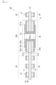
- FIG. 1 is a cross-sectional view showing a flexible printed wiring board according to a first embodiment of the present invention.
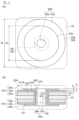
- 2(a) is an enlarged plan view of a portion II in FIG. 1
- FIG. 2(b) is an enlarged sectional view of the portion II in FIG. 3A to 3K are cross-sectional views showing a method for manufacturing a flexible printed wiring board according to the first embodiment of the present invention.
- FIG. 4 is a cross-sectional view showing a flexible printed wiring board according to a second embodiment of the present invention.
- 5(a) to 5(k) are cross-sectional views showing a method for manufacturing a flexible printed wiring board according to the second embodiment of the present invention.
- FIG. 1 is a cross-sectional view showing a flexible printed wiring board according to a first embodiment of the present invention.
- 2(a) is an enlarged plan view of a portion II in FIG. 1
- FIG. 2(b) is an enlarged sectional view of the portion II in FIG. 3A to 3K
- FIG. 6( a ) is a cross-sectional view showing a modified example of an interlayer connection portion of a flexible printed wiring board in the first embodiment
- FIG. 6( b ) is a cross-sectional view showing a modified example of an interlayer connection portion of a flexible printed wiring board in the second embodiment.
- Fig. 1 is a cross-sectional view showing a flexible printed wiring board 1A in a first embodiment.
- Fig. 2(a) is an enlarged plan view of part II in Fig. 1.
- Fig. 2(b) is an enlarged cross-sectional view of part II in Fig. 1.
- the flexible printed wiring board 1A in this embodiment is a double-sided flexible printed wiring board (FPC) having wiring patterns 20 on both sides.
- This flexible printed wiring board 1A includes an insulating substrate 10, wiring patterns 20, an interlayer connection 30A, and a through hole 50.
- the insulating substrate 10 corresponds to an example of an "insulating layer" in this aspect of the present invention
- the through hole 50 corresponds to an example of a "hole” in this aspect of the present invention.
- the insulating substrate 10 is a flexible resin film.
- the insulating substrate 10 is made of a material having electrical insulation properties, such as a resin material.
- materials constituting the insulating substrate 10 include polyimide (PI), liquid crystal polymer (LCP), polyethylene terephthalate (PET), polyethylene naphthalate (PEN), polyetherimide (PEI), polyether ether ketone (PEEK), and aramid.
- the insulating substrate 10 in this embodiment is an insulating film of flexible copper clad laminate (FCCL).
- a wiring pattern 20 is formed on the upper surface 11 and the lower surface 12 of the insulating substrate 10.
- the wiring pattern 20 includes linear thin wires 21 that are conductive.
- the wiring pattern 20 may also include pads, terminals, etc. in addition to the thin wires 21.
- the fine wire 21 includes a first metal foil layer 22 and a first panel plating layer 23.
- the first metal foil layer 22 is formed on each of the top and bottom surfaces 11, 12 of the insulating substrate 10.
- examples of materials constituting this first metal foil layer 22 include copper, silver, and gold.
- the first metal foil layer 22 in this embodiment is copper foil.
- the first panel plating layer 23 is formed on the first metal foil layer 22 by electrolytic panel plating.
- examples of materials constituting the first panel plating layer 23 include copper, silver, and gold.
- the first panel plating layer 23 in this embodiment is a copper plating layer formed by panel plating.
- the material constituting the first panel plating layer 23 may be the same material as the first metal foil layer 22, or may be a material different from the first metal foil layer 22.
- the interlayer connection portion 30A is formed from the upper surface 11 to the lower surface 12 of the insulating substrate 10 via a through hole 50.
- the through hole 50 is a cylindrical hole that penetrates the insulating substrate 10 and the second metal foil layers 32a, 32b (described below) that constitute the land portions 31a, 31b (described below).
- the interlayer connection portion 30A penetrates the insulating substrate 10 at the through hole 50, and the second metal foil layers 32a, 32b in the interlayer connection portion 30A are electrically connected to each other. Note that the interlayer connection portion 30A may or may not be connected to the wiring pattern 20.
- the interlayer connection portion 30A includes land portions 31a and 31b and a through-hole plating portion 35a.
- the land portion 31a has a circular ring shape concentric with the through hole 50, and is formed on the upper surface 11 so as to surround the through hole 50. More precisely, a part of the inner side of the land portion 31a is located inside the through hole 50 and is also located above the through hole 50.
- This land portion 31a includes a second metal foil layer 32a, a second panel plating layer 33a, and a first pattern plating layer 34a.
- the second metal foil layer 32a corresponds to an example of a "metal foil layer” of a flexible printed wiring board in this aspect of the present invention
- the second panel plating layer 33a corresponds to an example of a "third plating layer” in this aspect of the present invention
- the first pattern plating layer 34a corresponds to an example of a "fourth plating layer” in this aspect of the present invention.
- the second metal foil layer 32a is formed on the upper surface 11 of the insulating substrate 10. As shown in FIG. 2(a), the second metal foil layer 32a has a circular ring shape surrounding the through hole 50, and the inner peripheral surface 321 of the second metal foil layer 32a defines the upper portion of the through hole 50.
- examples of the material constituting the second metal foil layer 32a include copper, silver, and gold. Also, although not particularly limited, the second metal foil layer 32a in this embodiment is copper foil.
- a second panel plating layer 33a is formed on the inner circumferential surface 321 and the upper surface 322 of the second metal foil layer 32a.
- the second panel plating layer 33a covers the entire inner circumferential surface 321 and the upper surface 322 of the second metal foil layer 32a, and has a circular ring shape that follows the shape of the second metal foil layer 32a.
- This second panel plating layer 33 is formed on the second metal foil layer 32a by electrolytic panel plating.
- examples of the material constituting this second panel plating layer 33a include the same material as the first panel plating layer 23.
- the material constituting the second panel plating layer 33a may be a material different from that of the first panel plating layer 23.
- the thickness T2 of the second panel plating layer 33a may be, for example, 2 ⁇ m to 5 ⁇ m (2 ⁇ m ⁇ T2 ⁇ 5 ⁇ m), and the thickness T1 of the second metal foil layer 32a may be, for example, 5 ⁇ m to 12 ⁇ m (5 ⁇ m ⁇ T1 ⁇ 12 ⁇ m).
- a first pattern plating layer 34a is formed on the inner surface 331 and the upper surface 332 of the second panel plating layer 33a.
- materials constituting this first pattern plating layer 34a include copper, silver, and gold.
- the first pattern plating layer 34a in this embodiment is a copper plating layer formed on the second panel plating layer 33a near the through hole 50 by a pattern plating method (button plating method).
- the first pattern plating layer 34a has a ring shape that is concentric with the second panel plating layer 33a but has a different diameter from that of the second panel plating layer 33a. Specifically, the diameter R2 of the first pattern plating layer 34a is smaller than the diameter R1 of the second panel plating layer 33a ( R2 ⁇ R1 ).
- the first pattern plating layer 34a therefore covers the entire inner circumferential surface 331 of the second panel plating layer 33a, while covering only a portion of the upper surface 332 of the second panel plating layer 33a. This creates a step 311a on the upper surface 310 of the land portion 31a between the upper surface 342 of the first pattern plating layer 34a and the upper surface 332 of the second panel plating layer 33a.
- the thickness T3 of the first pattern plating layer 34a is 1/2 or less of the thickness T1 of the second metal foil layer 32a ( T3 ⁇ (1/2) ⁇ T1 ). Furthermore, although not particularly limited, the thickness T3 of the first pattern plating layer 34a may be 1/5 or more of the thickness T1 of the second metal foil layer 32a ( T3 ⁇ (1/5) ⁇ T1 ). By making the thickness T3 of the first pattern plating layer 34a 1/2 or less of the thickness T1 of the second metal foil layer 32a, the fine lines of the wiring pattern 20 can be formed with high precision. Although not particularly limited, the thickness T3 of the first pattern plating layer 34a may be, for example, 2 ⁇ m to 5 ⁇ m (2 ⁇ m ⁇ T3 ⁇ 5 ⁇ m).
- land portion 31b has a structure basically similar to that of land portion 31a described above, except that it is formed on the lower surface 12 of insulating substrate 10.
- land portion 31b has a circular ring shape concentric with through hole 50, and is formed on lower surface 12 so as to surround through hole 50. More precisely, a part of the inner side of land portion 31b is located inside through hole 50 and is also located below through hole 50.
- This land portion 31b includes a second metal foil layer 32b, a second panel plating layer 33b, and a first pattern plating layer 34b.
- the second metal foil layer 32b also corresponds to an example of a "metal foil layer” of the flexible printed wiring board in this aspect of the present invention
- the second panel plating layer 33b also corresponds to an example of a "third plating layer” in this aspect of the present invention
- the first pattern plating layer 34b also corresponds to an example of a "fourth plating layer” in this aspect of the present invention.
- This second metal foil layer 32b is covered with a second panel plating layer 33b, similar to the second metal foil layer 32a.
- This second panel plating layer 33b has a circular ring shape following the shape of the second metal foil layer 32b, similar to the second panel plating layer 33a.
- This second panel plating layer 33b is also formed on the second metal foil layer 32b by an electrolytic panel plating method.
- the material constituting this second panel plating layer 33b can be, for example, the same material as the first panel plating layer 23. However, the material constituting the second panel plating layer 33b may be a material different from that of the first panel plating layer 23.
- a first pattern plating layer 34b having a circular ring shape with a smaller diameter than the second panel plating layer 33b is formed on the second panel plating layer 33b.
- examples of the material constituting the first pattern plating layer 34b include the same material as the first pattern plating layer 34a.
- the material constituting the first pattern plating layer 34b may be a material different from that of the first pattern plating layer 34a.
- the first pattern plating layer 34b in this embodiment is a copper plating layer formed by a pattern plating method.
- the thickness of the second panel plating layer 33b and the thickness of the first pattern plating layer 34b are less than half the thickness of the second metal foil layer 32b.
- the through-hole plated portion 35a has a cylindrical shape that conforms to the inner wall of the through hole 50, and is formed on the insulating substrate 10 inside the through hole 50.
- the top and bottom of the through-hole plated portion 35a are sandwiched between the land portions 31a and 31b, thereby electrically connecting the land portions 31a and 31b to each other.
- the through-hole plating section 35a includes a third panel plating layer 36a and a second pattern plating layer 37a.
- the third panel plating layer 36a is formed on the insulating substrate 10 inside the through hole 50, and has a cylindrical shape extending along the thickness direction of the insulating substrate 10.
- This third panel plating layer 36a is formed integrally with the second panel plating layers 33a, 33b, and is made of the same material as the second panel plating layers 33a, 33b.
- the second pattern plating layer 37a is formed inside the through hole 50, on the inside of the third panel plating layer 36a, and has a cylindrical shape extending along the thickness direction of the insulating substrate 10.
- This second pattern plating layer 37a is formed integrally with the first pattern plating layers 34a, 34b, and is made of the same material as the first pattern plating layers 34a, 34b.
- the flexible printed wiring board 1A in this embodiment has land portions 31a, 31b including second panel plating layers 33a, 33b and first pattern plating layers 34a, 34b that are different in diameter from each other.
- the flexible printed wiring board 1A can be manufactured by the manufacturing method described below, so that the occurrence of defective formation of the wiring pattern 20 can be suppressed and connection reliability can be improved.
- FIGS. 3(a) to 3(k) are cross-sectional views showing the method for manufacturing the flexible printed wiring board 1A in this embodiment.
- a double-sided board 100 is prepared (preparation step).
- the double-sided board 100 comprises an insulating substrate 10 and metal foil layers 102a, 102b formed on the top and bottom surfaces 11, 12 of the insulating substrate 10.
- an example of the double-sided board 100 is a double-sided copper-clad laminate.
- the metal foil layer may be a metal other than copper, such as silver or gold.
- the double-sided board 100 corresponds to an example of a "substrate" in this aspect of the present invention.
- through holes 50 penetrating the insulating substrate 10 and the top and bottom surfaces 11, 12 are formed in the double-sided substrate 100 (hole drilling process).
- the through holes 50 can be formed in the double-sided substrate 100 using a laser, a drill, or the like.
- the through holes 50 may be subjected to a desmear process or a conductive process.
- the conductive process is a pre-processing process for the subsequent panel plating process, and may be, for example, a process of applying a conductive material to the inner wall of the through holes 50 by a process such as direct plating.
- a first plating layer 103 is formed on the double-sided board 100 by panel plating (panel plating process).
- Panel plating is generally a method of forming a plating layer on the entire surface of a board (manufacturing panel) and in the through holes by electrolytic plating.
- the first plating layer 103 is formed on the entire surfaces of the top and bottom surfaces 11, 12 including the periphery of the through hole 50, and inside the through hole 50 by panel plating.
- the panel plating process corresponds to an example of the first plating process in this aspect of the present invention.
- the thickness of the first plating layer 103 can be set to 1/2 or less of the thickness of the metal foil layers 102a and 102b.
- the thickness of the first plating layer 103 can be controlled by the electrolytic plating time and current density.
- a dry film 600 is applied as a plating resist to both sides of the double-sided substrate 100.
- this dry film 600 is a negative resist film, and the exposed portions are hardened and become insoluble in the developer, while the unexposed portions are soluble in the developer.
- This resist pattern 601 is a pattern for forming the first and second pattern plating layers 34a, 34b of the flexible printed wiring board 1A described above, and its outer shape corresponds to the outer shape of the first and second pattern plating layers 34a, 34b.
- a second plating layer 104 is formed around and inside the through hole 50 by pattern plating, and the dry film 600 is peeled off.
- the second plating layer 104 is formed only inside the resist pattern 601 by pattern plating, so that the second plating layer 104 can be formed on the first plating layer 103 around and inside the through hole 50.
- the dry film 600 can be peeled off with a general peeling solution or the like.
- the series of steps shown in FIG. 3(d) to FIG. 3(f) corresponds to an example of the "second plating step" in this aspect of the present invention.
- the thickness of the second plating layer 104 can be less than or equal to half the thickness of the metal foil layers 102a and 102b.
- the thickness of the second plating layer 104 can be controlled by the electrolytic plating time and current density.
- a dry film 700 is applied to both sides of the double-sided substrate 100 as an etching resist.
- the first and second plating layers 103, 104 are covered with the dry film 700.
- the dry film 700 may be, for example, the same as the dry film 600 described above.
- the dry film 700 is exposed and developed to form a resist pattern 701.
- the metal foil layers 102a and 102b, the first plating layer 103, and the second plating layer 104 are etched to form the wiring pattern 20 and the land portions 31a and 31b.
- the dry film 700 is peeled off.
- the dry film 700 can be peeled off with a general peeling solution or the like.
- the series of steps shown in FIG. 3(g) to FIG. 3(j) corresponds to an example of the "patterning step" in this embodiment of the present invention.
- the flexible printed wiring board 1A of this embodiment can be manufactured.
- the plating process includes a first plating process and a second plating process. This allows the plating layer in the land portions 31a and 31b to be gradually thinner toward the outside of the through hole, thereby reducing the step 311a. At the same time, a plating layer of sufficient thickness can be formed in the land portions 31a and 31b. As a result, it is possible to suppress the occurrence of defective formation of the wiring pattern 20 and improve the connection reliability in the land portions 31a and 31b.
- plating is performed so that the thickness of the first plating layer 103, the thickness of the second plating layer 104, and the thickness of the metal foil layers 102a and 102b are less than half.
- FIG. 4 is a cross-sectional view showing a flexible printed wiring board 1B in a second embodiment of the present invention.
- the flexible printed wiring board 1B in the second embodiment is different from the flexible printed wiring board 1A in the first embodiment in that a panel plating layer is formed on the pattern plating layer at the interlayer connection portion 30B.
- the other configurations are similar to those of the first embodiment. Below, only the differences between the flexible printed wiring board 1B in the second embodiment and the first embodiment will be described, and the same configurations as those in the first embodiment will be denoted by the same reference numerals and will not be described.
- the interlayer connection portion 30B in the second embodiment includes land portions 31c and 31d and a through-hole plating portion 35b.
- first pattern plating layers 34c and 34d are formed on the second metal foil layers 32a and 32b, respectively.
- Second panel plating layers 33c and 33d are further formed on the second metal foil layers 32a and 32b and the first pattern plating layers 34c and 34d.
- the first pattern plating layers 34c and 34d correspond to an example of a "third plating layer” in this aspect of the present invention
- the second panel plating layers 33c and 33d correspond to an example of a "fourth plating layer" in this aspect of the present invention.
- a step 311b is also formed in the land portions 31c and 31d, but this step 311b is formed by bending the second panel plating layers 33c and 33d in the thickness direction of the insulating substrate 10 to follow the shape of the outer peripheral ends of the first pattern plating layers 34c and 34d.
- a second pattern plating layer 37b is formed on the insulating substrate 10, and a third panel plating layer 36b is formed on this second pattern plating layer 37b.
- the flexible printed wiring board 1B as described above can make the plating layer in the land portions 31c and 31d thinner in stages toward the outside of the through hole 50, thereby making the step 311b smaller.
- a plating layer of sufficient thickness can be formed in the land portions 31c and 31d. As a result, it is possible to suppress the occurrence of defective formation of the wiring pattern 20 and improve the connection reliability in the land portions 31c and 31d.
- FIG. 5(a) to FIG. 5(k) are cross-sectional views showing a manufacturing method for a flexible printed wiring board 1B in this embodiment.
- a double-sided substrate 100 is prepared in the same manner as in the first embodiment (preparation process).
- through holes 50 penetrating the insulating substrate 10 and the top and bottom surfaces 11, 12 are formed in the double-sided substrate 100 (hole drilling process).
- a dry film 600 is applied as a plating resist to both sides of the double-sided board 100.
- the entire surfaces of the metal foil layers 102a and 102b and the through holes 50 are covered with the dry film 600.
- This resist pattern 601 is a pattern for forming the first and second pattern plating layers 34c, 34d of the flexible printed wiring board 1B described above, and its outer shape corresponds to the outer shape of the first and second pattern plating layers 34c, 34d.
- a second plating layer 104 is formed around the through hole 50 and inside the through hole 50 by pattern plating, and the dry film 600 is peeled off.
- This second plating layer 104 is the above-mentioned first to third pattern plating layers 34c, 34d, and 36b.
- the series of steps shown in FIG. 5(c) to FIG. 5(e) corresponds to an example of the "second plating step" in this aspect of the present invention.
- a first plating layer 103 is formed on the double-sided substrate 100 by panel plating.
- the first plating layer 103 is also formed on the second plating layer 104 around and inside the through hole 50.
- the process shown in FIG. 5(f) corresponds to an example of a "first plating process" in this aspect of the present invention.
- a dry film 700 is attached to both sides of the double-sided substrate 100 as an etching resist.
- the dry film 700 is exposed and developed to form a resist pattern 701.
- the metal foil layers 102a and 102b, the second plating layer 104, and the first plating layer 103 are etched to form the wiring pattern 20 and the land portions 31c and 31d.
- the dry film 700 is peeled off.
- the flexible printed wiring board 1B of this embodiment can be manufactured.
- the through holes 50 are formed in the flexible printed wiring boards 1A and 1B, but this is not limited to this.
- a bottomed hole may be formed instead of the through hole 50.
- the land portion is formed only on one side of the flexible printed wiring boards 1A and 1B.
- FIG. 6(a) is a cross-sectional view showing a modified interlayer connection portion 30A of a flexible printed wiring board 1A in the first embodiment
- FIG. 6(b) is a cross-sectional view showing a modified interlayer connection portion 30B of a flexible printed wiring board in the second embodiment.
- the bottomed hole 55 in the modified example of the first embodiment penetrates the insulating substrate 10 and the second metal foil layer 32b.
- the bottom of the bottomed hole 55 is blocked by the metal foil layer 102b.
- the second panel plating layer 33a and the first pattern plating layer 34a are also formed at the bottom of the bottomed hole 55.
- Such second panel plating layer 33a and first pattern plating layer 34a can be formed in a procedure basically similar to the first and second plating steps described in FIG. 3.
- the bottom of the bottomed hole 55 in the modified example of the second embodiment is also blocked by a metal foil layer 102b.
- the first pattern plating layer 34c and the second panel plating layer 33c are also formed on the bottom of the bottomed hole 55.
- Such first pattern plating layer 34c and second panel plating layer 33c can be formed in a procedure basically similar to the first and second plating steps described in FIG. 5.
Landscapes
- Engineering & Computer Science (AREA)
- Microelectronics & Electronic Packaging (AREA)
- Manufacturing & Machinery (AREA)
- Printing Elements For Providing Electric Connections Between Printed Circuits (AREA)
Priority Applications (3)
| Application Number | Priority Date | Filing Date | Title |
|---|---|---|---|
| JP2025531462A JPWO2025009357A1 (https=) | 2023-07-03 | 2024-06-13 | |
| CN202480041476.1A CN121359596A (zh) | 2023-07-03 | 2024-06-13 | 柔性印刷布线板的制造方法及柔性印刷布线板 |
| KR1020257042930A KR20260014642A (ko) | 2023-07-03 | 2024-06-13 | 플렉시블 프린트 배선판의 제조 방법 및 플렉시블 프린트 배선판 |
Applications Claiming Priority (2)
| Application Number | Priority Date | Filing Date | Title |
|---|---|---|---|
| JP2023-109563 | 2023-07-03 | ||
| JP2023109563 | 2023-07-03 |
Publications (1)
| Publication Number | Publication Date |
|---|---|
| WO2025009357A1 true WO2025009357A1 (ja) | 2025-01-09 |
Family
ID=94171710
Family Applications (1)
| Application Number | Title | Priority Date | Filing Date |
|---|---|---|---|
| PCT/JP2024/021580 Ceased WO2025009357A1 (ja) | 2023-07-03 | 2024-06-13 | フレキシブルプリント配線板の製造方法及びフレキシブルプリント配線板 |
Country Status (4)
| Country | Link |
|---|---|
| JP (1) | JPWO2025009357A1 (https=) |
| KR (1) | KR20260014642A (https=) |
| CN (1) | CN121359596A (https=) |
| WO (1) | WO2025009357A1 (https=) |
Citations (5)
| Publication number | Priority date | Publication date | Assignee | Title |
|---|---|---|---|---|
| JPS63254793A (ja) * | 1987-04-11 | 1988-10-21 | ソニー株式会社 | プリント配線基板の製造方法 |
| JPH04100294A (ja) * | 1990-08-20 | 1992-04-02 | Mitsubishi Rayon Co Ltd | プリント配線板の製造方法 |
| JPH05235200A (ja) * | 1992-02-24 | 1993-09-10 | Ibiden Co Ltd | 電子部品搭載用基板 |
| JP2009088334A (ja) | 2007-10-01 | 2009-04-23 | Nippon Mektron Ltd | プリント配線板の製造方法 |
| JP2023109563A (ja) | 2022-01-27 | 2023-08-08 | 大王製紙株式会社 | 吸収性物品 |
-
2024
- 2024-06-13 CN CN202480041476.1A patent/CN121359596A/zh active Pending
- 2024-06-13 WO PCT/JP2024/021580 patent/WO2025009357A1/ja not_active Ceased
- 2024-06-13 JP JP2025531462A patent/JPWO2025009357A1/ja active Pending
- 2024-06-13 KR KR1020257042930A patent/KR20260014642A/ko active Pending
Patent Citations (5)
| Publication number | Priority date | Publication date | Assignee | Title |
|---|---|---|---|---|
| JPS63254793A (ja) * | 1987-04-11 | 1988-10-21 | ソニー株式会社 | プリント配線基板の製造方法 |
| JPH04100294A (ja) * | 1990-08-20 | 1992-04-02 | Mitsubishi Rayon Co Ltd | プリント配線板の製造方法 |
| JPH05235200A (ja) * | 1992-02-24 | 1993-09-10 | Ibiden Co Ltd | 電子部品搭載用基板 |
| JP2009088334A (ja) | 2007-10-01 | 2009-04-23 | Nippon Mektron Ltd | プリント配線板の製造方法 |
| JP2023109563A (ja) | 2022-01-27 | 2023-08-08 | 大王製紙株式会社 | 吸収性物品 |
Also Published As
| Publication number | Publication date |
|---|---|
| KR20260014642A (ko) | 2026-01-30 |
| CN121359596A (zh) | 2026-01-16 |
| JPWO2025009357A1 (https=) | 2025-01-09 |
Similar Documents
| Publication | Publication Date | Title |
|---|---|---|
| KR100346400B1 (ko) | 다층 인쇄회로기판 및 그 제조방법 | |
| CN206461833U (zh) | 软硬结合板结构 | |
| JP2005183952A (ja) | 導電孔を有したプリント回路ボードの製造方法及びボード | |
| KR20070082537A (ko) | 회로 기판 구조체 및 그 제조 방법 | |
| JP2007142403A (ja) | プリント基板及びその製造方法 | |
| JP2009260204A (ja) | プリント基板およびその製造方法 | |
| JP2012094662A (ja) | 多層配線基板の製造方法 | |
| JP2004146836A (ja) | 回路基板及びその製造方法 | |
| KR100965341B1 (ko) | 인쇄회로기판의 제조방법 | |
| JP2001053188A (ja) | 多層配線基板の製造方法 | |
| KR20060106766A (ko) | 전해 도금을 이용한 회로 기판의 제조 방법 | |
| JP2005191100A (ja) | 半導体基板及びその製造方法 | |
| WO2025009357A1 (ja) | フレキシブルプリント配線板の製造方法及びフレキシブルプリント配線板 | |
| KR102886869B1 (ko) | 프린트 배선판의 제조 방법 | |
| KR100294157B1 (ko) | 다층인쇄회로기판의층간전기접속방법 | |
| JP4606018B2 (ja) | プリント配線板の製造方法 | |
| JP2000323841A (ja) | 多層回路基板とその製造方法 | |
| US20070132087A1 (en) | Via hole having fine hole land and method for forming the same | |
| TW201941671A (zh) | 軟硬複合板及其製法 | |
| TWI505759B (zh) | 印刷電路板及其製造方法 | |
| JP2005108941A (ja) | 多層配線板及びその製造方法 | |
| JP4059386B2 (ja) | 多層プリント配線板およびその製造方法 | |
| JP7505963B2 (ja) | 印刷配線板 | |
| KR101480557B1 (ko) | 인쇄회로기판 및 그 제조방법 | |
| JP2005109299A (ja) | 多層配線板およびその製造方法 |
Legal Events
| Date | Code | Title | Description |
|---|---|---|---|
| 121 | Ep: the epo has been informed by wipo that ep was designated in this application |
Ref document number: 24835873 Country of ref document: EP Kind code of ref document: A1 |
|
| ENP | Entry into the national phase |
Ref document number: 2025531462 Country of ref document: JP Kind code of ref document: A |
|
| WWE | Wipo information: entry into national phase |
Ref document number: 2025531462 Country of ref document: JP |
|
| ENP | Entry into the national phase |
Ref document number: 1020257042930 Country of ref document: KR Free format text: ST27 STATUS EVENT CODE: A-0-1-A10-A15-NAP-PA0105 (AS PROVIDED BY THE NATIONAL OFFICE) |
|
| WWE | Wipo information: entry into national phase |
Ref document number: 1020257042930 Country of ref document: KR |
|
| WWP | Wipo information: published in national office |
Ref document number: 1020257042930 Country of ref document: KR |
|
| WWE | Wipo information: entry into national phase |
Ref document number: 2024835873 Country of ref document: EP |
|
| NENP | Non-entry into the national phase |
Ref country code: DE |
|
| ENP | Entry into the national phase |
Ref document number: 2024835873 Country of ref document: EP Effective date: 20260203 |