WO2025005037A1 - 樹脂組成物及び接続構造体の製造方法 - Google Patents
樹脂組成物及び接続構造体の製造方法 Download PDFInfo
- Publication number
- WO2025005037A1 WO2025005037A1 PCT/JP2024/022797 JP2024022797W WO2025005037A1 WO 2025005037 A1 WO2025005037 A1 WO 2025005037A1 JP 2024022797 W JP2024022797 W JP 2024022797W WO 2025005037 A1 WO2025005037 A1 WO 2025005037A1
- Authority
- WO
- WIPO (PCT)
- Prior art keywords
- resin composition
- flux
- electrode
- solder
- weight
- Prior art date
- Legal status (The legal status is an assumption and is not a legal conclusion. Google has not performed a legal analysis and makes no representation as to the accuracy of the status listed.)
- Ceased
Links
Images


Classifications
-
- H—ELECTRICITY
- H01—ELECTRIC ELEMENTS
- H01B—CABLES; CONDUCTORS; INSULATORS; SELECTION OF MATERIALS FOR THEIR CONDUCTIVE, INSULATING OR DIELECTRIC PROPERTIES
- H01B1/00—Conductors or conductive bodies characterised by the conductive materials; Selection of materials as conductors
- H01B1/20—Conductive material dispersed in non-conductive organic material
- H01B1/22—Conductive material dispersed in non-conductive organic material the conductive material comprising metals or alloys
-
- H—ELECTRICITY
- H01—ELECTRIC ELEMENTS
- H01B—CABLES; CONDUCTORS; INSULATORS; SELECTION OF MATERIALS FOR THEIR CONDUCTIVE, INSULATING OR DIELECTRIC PROPERTIES
- H01B5/00—Non-insulated conductors or conductive bodies characterised by their form
- H01B5/16—Non-insulated conductors or conductive bodies characterised by their form comprising conductive material in insulating or poorly conductive material, e.g. conductive rubber
-
- H—ELECTRICITY
- H10—SEMICONDUCTOR DEVICES; ELECTRIC SOLID-STATE DEVICES NOT OTHERWISE PROVIDED FOR
- H10W—GENERIC PACKAGES, INTERCONNECTIONS, CONNECTORS OR OTHER CONSTRUCTIONAL DETAILS OF DEVICES COVERED BY CLASS H10
- H10W72/00—Interconnections or connectors in packages
- H10W72/071—Connecting or disconnecting
Definitions
- the present invention relates to a resin composition containing solder particles.
- the present invention also relates to a method for manufacturing a connection structure using the resin composition.
- Anisotropic conductive materials such as anisotropic conductive pastes and anisotropic conductive films are widely known.
- anisotropic conductive materials conductive particles are dispersed in a binder. Solder particles are widely used as the above conductive particles.
- the anisotropic conductive material is used to obtain various connection structures.
- connections using the anisotropic conductive material include connections between a flexible printed circuit board and a glass substrate (FOG (Film on Glass)), connections between a semiconductor chip and a flexible printed circuit board (COF (Chip on Film)), connections between a semiconductor chip and a glass substrate (COG (Chip on Glass)), and connections between a flexible printed circuit board and a glass epoxy substrate (FOB (Film on Board)).
- connection structures In recent years, devices using connection structures have become smaller and lighter. This has led to a demand for the development of connection structures using fine semiconductor chips such as micro-LED (micro-light emitting diode) chips. Laser transfer methods have attracted attention as a method for placing fine semiconductor chips such as micro-LED chips on circuit boards.
- micro-LED micro-light emitting diode
- Patent Document 1 discloses a laser transfer device.
- a source substrate on which multiple elements are formed is placed above a destination substrate.
- multiple target elements that are the targets of transfer among the multiple elements are moved downward, and the target elements are transferred to the destination substrate.
- Patent Document 2 discloses a transfer method in which a chip component held on a transfer substrate via a photocurable adhesive layer is used to transfer the chip component to a destination substrate.
- the transfer method includes an exposure step in which the adhesive layer is exposed to light of a wavelength that hardens the adhesive layer in a pattern to partially reduce the adhesive strength of the adhesive layer, and a laser lift-off step in which the chip component is transferred to the destination substrate by a laser lift-off method after the exposure step.
- multiple semiconductor chips can be moved and mounted in one go from a wafer substrate (source substrate) to a circuit board (destination substrate), which can increase the productivity of connection structures.
- the object of the present invention is to provide a resin composition that can improve the capture of semiconductor chips flying at high speed. It is also an object of the present invention to provide a method for manufacturing a connection structure using the above resin composition.
- This specification discloses the following resin composition and a method for manufacturing a connection structure using the resin composition.
- Item 1 A resin composition comprising a thermosetting component, a flux, a thixotropic agent that is liquid at 25°C, and solder particles.
- the hydrogen bond term ⁇ H in the Hansen solubility parameter of the thixotropic agent is 10 MPa 1/2 or more
- the carbon number of the main chain of the first flux is an even number of 4 to 14
- the carbon number of the main chain of the second flux is an odd number of 3 to 11.
- Item 4 The resin composition according to item 2 or 3, wherein the average particle size of the first flux is 10 ⁇ m or less.
- Item 5 The resin composition according to any one of items 2 to 4, wherein the second flux is soluble in the thixotropic agent at 25°C.
- Item 6 The resin composition according to any one of items 2 to 5, wherein the content of the second flux is 1% by weight or more and 20% by weight or less in 100% by weight of the resin composition.
- Item 8 The resin composition according to any one of items 1 to 7, wherein the content of the flux is 5% by weight or more and 25% by weight or less in 100% by weight of the resin composition.
- Item 9 The resin composition according to any one of items 1 to 8, wherein the average particle size of the solder particles is 10 ⁇ m or less.
- Item 11 The method for producing a connection structure according to Item 10, in which, in the second placement step, the second connection target member is moved by a laser transfer method at a speed of 1 cm/s or more on the surface of the resin composition opposite the first connection target member, and the second connection target member is placed so that the first electrode and the second electrode face each other.
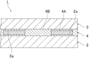
- FIG. 1 is a cross-sectional view that illustrates a connection structure obtained by using a resin composition according to one embodiment of the present invention.
- FIG. 2 is a cross-sectional view illustrating the steps of an example of a method for producing a connection structure using a resin composition according to one embodiment of the present invention.
- FIG. 3 is a cross-sectional view illustrating the steps of an example of a method for producing a connection structure using a resin composition according to one embodiment of the present invention.
- FIG. 4 is a cross-sectional view illustrating the steps of an example of a method for producing a connection structure using a resin composition according to one embodiment of the present invention.
- FIG. 5 is a cross-sectional view showing a modified example of the connection structure.
- the resin composition according to the present invention contains a thermosetting component, a flux, a thixotropic agent that is liquid at 25° C., and solder particles.
- the resin composition according to the present invention has the above-mentioned configuration, and therefore can improve the capture of semiconductor chips arriving at high speed.
- the laser transfer method can improve the capture of semiconductor chips arriving at high speed.
- the arriving semiconductor chip can be accurately positioned at a predetermined location on the circuit board (connection target component) (effectively suppressing misalignment during placement of the semiconductor chip).
- the above resin composition is placed on the surface of the connection target member (circuit board, transfer destination substrate) and used in the method for manufacturing a connection structure.
- the above resin composition is suitably used in the method for manufacturing a connection structure to effectively capture a semiconductor chip flying at high speed by a laser transfer method.
- the above resin composition is preferably a resin composition for capturing a semiconductor chip by a laser transfer method.
- the resin composition according to the present invention is preferably used for connecting semiconductor chips by laser transfer method (use of resin composition for connecting semiconductor chips by laser transfer method). More specifically, the resin composition according to the present invention is more preferably used for connecting semiconductor chips to a substrate by laser transfer method (use of resin composition for connecting semiconductor chips to a substrate by laser transfer method).
- the contact angle of the resin composition with water at 25°C is preferably 65° or less, more preferably 60° or less, even more preferably 55° or less, and particularly preferably 45° or less.
- the contact angle of the resin composition with water at 25°C is the above upper limit or less, the capture of the semiconductor chip flying at high speed by the laser transfer method can be further improved.
- the electrodes of the semiconductor chip generally contain gold, copper, or an alloy thereof, and therefore the surface of the electrode of the semiconductor chip is often hydrophilic.
- the contact angle of the resin composition of the present invention with water at 25°C is the above upper limit or less, the surface of the resin composition has hydrophilicity, so that the affinity with the surface of the electrode of the semiconductor chip is high, and when the resin composition is placed on the surface of the connection target member (circuit board), the capture of the semiconductor chip flying at high speed by the laser transfer method can be further improved.
- the lower limit of the contact angle of the resin composition with water at 25°C is not particularly limited.
- the contact angle of the resin composition with water at 25°C may be 0° or more, may exceed 0°, may be 1° or more, or may be 5° or more.
- the range of the contact angle can be set by appropriately selecting the lower limit and the upper limit.
- the contact angle of the resin composition with water at 25°C can be measured, for example, by the following method. 1 ml of water is dropped onto the surface of the resin composition, and the contact angle of the resin composition with water is measured using a contact angle measuring device.
- An example of the contact angle measuring device is Kyowa's "DMo-601."
- the contact angle of the resin composition with water at 25°C is measured 10 seconds after the water is placed on the surface of the resin composition.
- the contact angle of the resin composition with water at 25°C can be adjusted by the following methods: Combining multiple skeletons of a thermosetting component such as an epoxy resin. Selecting the skeleton of a thermosetting component such as an epoxy resin. Selecting the side chain of a thermosetting component such as an epoxy resin. Dispersing an additive that is liquid at 25°C into the resin composition.
- the resin composition is preferably in a liquid state at 25°C.
- a paste state is included in the liquid state.
- the resin composition is preferably in a paste state at 25°C.
- the resin composition is a conductive material since it contains solder particles.
- the resin composition is preferably a conductive paste.
- the resin composition is preferably a conductive paste at 25°C. In these cases, the resin composition can be applied more thinly and effectively onto the surface of the connection target member, the laser transfer method can more effectively increase the capture of semiconductor chips flying at high speed, and the cohesion of the solder during conductive connection can be more effectively increased.
- the viscosity ( ⁇ 25) of the resin composition at 25°C is preferably 30 Pa ⁇ s or more, more preferably 50 Pa ⁇ s or more, and preferably 250 Pa ⁇ s or less, more preferably 200 Pa ⁇ s or less.
- the viscosity ( ⁇ 25) is equal to or greater than the lower limit, the capture of semiconductor chips flying at high speed by the laser transfer method can be more effectively improved.
- the viscosity ( ⁇ 25) is equal to or less than the upper limit, the resin composition can be applied thinly and satisfactorily to the surface of the connection target component, and the cohesiveness of the solder during conductive connection can be effectively improved.
- the viscosity ( ⁇ 25) can be adjusted as appropriate by the types and amounts of the components.
- the above viscosity ( ⁇ 25) can be measured, for example, using an E-type viscometer (Toki Sangyo Co., Ltd.'s "TVE-22L”) at 25°C and 5 rpm.
- E-type viscometer Toki Sangyo Co., Ltd.'s "TVE-22L"
- the viscosity ( ⁇ mp) of the resin composition at the melting point of the solder particles is preferably 0.1 Pa ⁇ s or more, more preferably 1 Pa ⁇ s or more, and preferably 10 Pa ⁇ s or less, more preferably 5 Pa ⁇ s or less.
- the viscosity ( ⁇ mp) can be adjusted as appropriate depending on the type and amount of the blended components.
- the viscosity ( ⁇ mp) is equal to or greater than the lower limit and equal to or less than the upper limit, the cohesiveness of the solder during conductive connection can be more effectively increased, voids at the connection portion can be more effectively suppressed, and the overflow of the resin composition to areas other than the connection portion can be more effectively suppressed.
- the viscosity ( ⁇ mp) is equal to or greater than the lower limit and equal to or less than the upper limit, the insulation reliability between electrodes can be more effectively increased, and the conduction reliability between electrodes can be more effectively increased.
- the above viscosity ( ⁇ mp) can be measured, for example, using a viscoelasticity measuring device ("HAAKE" manufactured by SCIENTIFIC) under conditions of stress control of 1 Pa, frequency of 1 Hz, heating rate of 20°C/min, and measurement temperature range of 25°C to 200°C. However, if the melting point of the solder particles exceeds 200°C, the upper temperature limit is set to the melting point of the solder particles. In this measurement, the viscosity ( ⁇ mp) is calculated by reading the viscosity at the melting point of the solder particles.
- HAAKE viscoelasticity measuring device
- the resin composition can be used as a conductive paste, a conductive film, and the like.
- the conductive paste is preferably an anisotropic conductive paste
- the conductive film is preferably an anisotropic conductive film.
- the resin composition is preferably in the form of a paste, and is preferably a conductive paste.
- the resin composition is suitably used for electrically connecting electrodes.
- the resin composition is preferably a circuit connecting material.
- (meth)acrylate refers to acrylate and methacrylate.
- (meth)acrylic refers to acrylic and methacrylic.
- (meth)acryloyl refers to acryloyl and methacryloyl.
- the resin composition according to the present invention includes a thermosetting component.
- the thermosetting component preferably includes a thermosetting compound.
- the resin composition may or may not include a thermosetting agent as a thermosetting component. Since the resin composition according to the present invention has the above configuration, even if the resin composition does not include a thermosetting agent, it can enhance the capture of a semiconductor chip flying at high speed by a laser transfer method. From the viewpoint of more effectively enhancing the cohesiveness of the solder during conductive connection, it is preferable that the resin composition does not include a thermosetting agent.
- the resin composition may include a curing accelerator as a thermosetting component.
- thermosetting component thermosetting compound
- the resin composition according to the present invention preferably contains a thermosetting compound.
- the thermosetting compound is a compound that can be cured by heating. There is no particular limitation on the thermosetting compound.
- the thermosetting compound Examples of the curable resin composition include an oxetane compound, an epoxy compound, an episulfide compound, a (meth)acrylic compound, a phenol compound, an amino compound, an unsaturated polyester compound, a polyurethane compound, a silicone compound, and a polyimide compound.
- the thermosetting compound is preferably an epoxy compound or an episulfide compound, and more preferably an epoxy compound. It is preferable that the thermosetting compound contains an epoxy compound, and it is more preferable that the thermosetting compound contains an epoxy compound.
- the thermosetting compound may be used alone or in combination of two or more kinds.
- the epoxy compound is a compound having at least one epoxy group.
- the epoxy compound include bisphenol A type epoxy compounds, bisphenol F type epoxy compounds, bisphenol S type epoxy compounds, phenol novolac type epoxy compounds, biphenyl type epoxy compounds, biphenyl novolac type epoxy compounds, biphenol type epoxy compounds, naphthalene type epoxy compounds, fluorene type epoxy compounds, phenol aralkyl type epoxy compounds, naphthol aralkyl type epoxy compounds, dicyclopentadiene type epoxy compounds, anthracene type epoxy compounds, epoxy compounds having an adamantane skeleton, epoxy compounds having a tricyclodecane skeleton, naphthylene ether type epoxy compounds, and epoxy compounds having a triazine nucleus in the skeleton.
- the epoxy compounds may be used alone or in combination of two or more.
- the epoxy compound is liquid or solid at room temperature (25°C), and when the epoxy compound is solid at room temperature, the melting temperature of the epoxy compound is preferably equal to or lower than the melting point of the solder particles.
- the viscosity is high at the stage of bonding the connection target components, and when acceleration is applied due to an impact from transportation, etc., it is possible to suppress misalignment between the connection target components (circuit board) and the semiconductor chip.
- the viscosity of the resin composition can be significantly reduced by the heat during curing, allowing the aggregation of the solder during conductive connection to proceed efficiently.
- thermosetting component contains an epoxy compound, and it is preferable that the thermosetting compound contains an epoxy compound.
- thermosetting compound contains a thermosetting compound having a polyether skeleton.
- thermosetting compounds having a polyether skeleton include compounds having glycidyl ether groups at both ends of an alkyl chain having 3 to 12 carbon atoms, and polyether-type epoxy compounds having a polyether skeleton having 2 to 4 carbon atoms and having structural units in which 2 to 10 polyether skeletons are bonded in succession.
- thermosetting compound contains a thermosetting compound having an isocyanuric skeleton.
- thermosetting compounds having an isocyanuric skeleton include triisocyanurate type epoxy compounds, such as the TEPIC series (TEPIC-G, TEPIC-S, TEPIC-SS, TEPIC-HP, TEPIC-L, TEPIC-PAS, TEPIC-VL, and TEPIC-UC) manufactured by Nissan Chemical Industries, Ltd.
- TEPIC series TEPIC-G, TEPIC-S, TEPIC-SS, TEPIC-HP, TEPIC-L, TEPIC-PAS, TEPIC-VL, and TEPIC-UC
- thermosetting compound has high heat resistance, and it is more preferable that the thermosetting compound contains a novolac type epoxy compound. Novolac type epoxy compounds have relatively high heat resistance.
- the content of the thermosetting compound is preferably 5% by weight or more, more preferably 8% by weight or more, even more preferably 10% by weight or more, and preferably 99% by weight or less, more preferably 90% by weight or less, even more preferably 80% by weight or less, and particularly preferably 70% by weight or less.
- the content of the thermosetting compound is equal to or more than the lower limit and equal to or less than the upper limit, the capture of semiconductor chips flying at high speed by the laser transfer method can be more effectively improved, solder can be more efficiently arranged on the electrodes, the insulation reliability between the electrodes can be more effectively improved, and the conduction reliability between the electrodes can be more effectively improved. From the viewpoint of more effectively improving the impact resistance of the resulting connection structure, the content of the thermosetting compound is preferably large.
- the content of the epoxy compound is preferably 5% by weight or more, more preferably 8% by weight or more, even more preferably 10% by weight or more, and preferably 99% by weight or less, more preferably 90% by weight or less, even more preferably 80% by weight or less, and particularly preferably 70% by weight or less.
- the content of the epoxy compound is equal to or more than the lower limit and equal to or less than the upper limit, the capture of semiconductor chips flying at high speed by the laser transfer method can be more effectively improved, solder can be more efficiently arranged on the electrodes, the insulation reliability between the electrodes can be more effectively improved, and the conduction reliability between the electrodes can be more effectively improved.
- the content of the epoxy compound is preferably high.
- the content of the novolac type epoxy compound is preferably 1% by weight or more, more preferably 3% by weight or more, even more preferably 5% by weight or more, and preferably 99% by weight or less, more preferably 90% by weight or less, even more preferably 80% by weight or less, and particularly preferably 70% by weight or less.
- the content of the novolac type epoxy compound is equal to or more than the lower limit and equal to or less than the upper limit, the capture of semiconductor chips flying at high speed by the laser transfer method can be more effectively improved, solder can be more efficiently arranged on the electrodes, the insulation reliability between the electrodes can be more effectively improved, and the conduction reliability between the electrodes can be more effectively improved. From the viewpoint of further improving the impact resistance of the resulting connection structure, the content of the novolac type epoxy compound is preferably large.
- the resin composition contains a flux, which can more effectively increase the cohesion of the solder during conductive connection.
- the above-mentioned fluxes include zinc chloride, a mixture of zinc chloride and an inorganic halide, a mixture of zinc chloride and an inorganic acid, a molten salt, phosphoric acid, a derivative of phosphoric acid, an organic acid, an organic acid amine salt, an organic halide, hydrazine, an amine compound other than an organic acid amine salt, and rosin. Only one type of the above-mentioned fluxes may be used, or two or more types may be used in combination.
- the flux preferably contains an organic acid or an organic acid amine salt.
- the organic acid is preferably a dicarboxylic acid
- the organic acid amine salt is preferably a dicarboxylic acid amine salt.
- the flux preferably contains a dicarboxylic acid or a dicarboxylic acid amine salt, and more preferably contains a dicarboxylic acid and a dicarboxylic acid amine salt.
- the dicarboxylic acids include glutaric acid, adipic acid, azelaic acid, and pimelic acid.
- dicarboxylic acid amine salts examples include benzylamine glutaric acid salt, benzylamine adipate salt, benzylamine azelaic acid salt, stearylamine glutaric acid salt, stearylamine adipate salt, and stearylamine azelaic acid salt.
- the flux is preferably solid.
- the flux may be spherical, may have a shape other than spherical, or may be flat.
- the flux contains two or more types of fluxes having different numbers of carbon atoms in the main chain. From the viewpoint of more effectively increasing the capture of semiconductor chips flying at high speed by the laser transfer method, it is preferable that the flux contains a first flux having an even number of carbon atoms in the main chain and a second flux having an odd number of carbon atoms in the main chain.
- the first flux only one type of flux may be used, or two or more types of flux may be used.
- the second flux only one type of flux may be used, or two or more types of flux may be used.
- the number of carbon atoms in the main chain of the first flux is an even number.
- the number of carbon atoms in the main chain of the first flux is an even number, and the number of carbon atoms in the main chain of the first flux is preferably 4 or more, more preferably 6 or more, and preferably 14 or less, more preferably 12 or less, even more preferably 10 or less, and particularly preferably 8 or less.
- the number of carbon atoms in the main chain of the first flux is preferably an even number between 4 and 14.
- the number of carbon atoms in the main chain of the second flux is an odd number.
- the number of carbon atoms in the main chain of the second flux is an odd number, and the number of carbon atoms in the main chain of the second flux is preferably 3 or more, and preferably 11 or less, more preferably 9 or less, and even more preferably 7 or less.
- the number of carbon atoms in the main chain of the second flux is preferably an odd number between 3 and 11.
- the average particle diameter of the flux (average particle diameter of the entire flux) is preferably 10 ⁇ m or less, more preferably 7 ⁇ m or less, even more preferably 5 ⁇ m or less, and particularly preferably 3 ⁇ m or less.
- the average particle diameter of the flux may be 0.01 ⁇ m or more, 0.1 ⁇ m or more, 0.5 ⁇ m or more, or 1.0 ⁇ m or more.
- the range of the average particle diameter of the flux can be set by appropriately selecting the lower limit and upper limit.
- the average particle diameter of the first flux is preferably 10 ⁇ m or less, more preferably 7 ⁇ m or less, and even more preferably 5 ⁇ m or less.
- the lower limit of the average particle diameter of the first flux is not particularly limited.
- the average particle diameter of the first flux may be 0.5 ⁇ m or more, or 1.0 ⁇ m or more.
- the range of the average particle diameter of the first flux can be set by appropriately selecting the lower limit and the upper limit.
- the average particle diameter of the second flux is preferably 7 ⁇ m or less, more preferably 5 ⁇ m or less, and even more preferably 3 ⁇ m or less.
- the lower limit of the average particle diameter of the second flux is not particularly limited.
- the average particle diameter of the second flux may be 0.01 ⁇ m or more, or may be 0.1 ⁇ m or more.
- the range of the average particle diameter of the second flux can be set by appropriately selecting the lower limit value and the upper limit value.
- the average particle diameter of the flux and the average particle diameters of the first and second fluxes are number average particle diameters.
- the average particle diameter of the flux and the average particle diameters of the first and second fluxes are obtained, for example, by observing 50 arbitrary fluxes with an electron microscope or optical microscope and calculating the average particle diameter of each flux, or by performing laser diffraction particle size distribution measurement. In observation with an electron microscope or optical microscope, the particle diameter of each flux is obtained as the particle diameter of a circle equivalent diameter. In observation with an electron microscope or optical microscope, the average particle diameter of 50 arbitrary fluxes with a circle equivalent diameter is almost equal to the average particle diameter of a sphere equivalent diameter.
- the particle diameter of each flux is obtained as the particle diameter of a sphere equivalent diameter. It is preferable that the average particle diameter of the flux and the average particle diameters of the first and second fluxes are calculated by laser diffraction particle size distribution measurement.
- the above flux and the first and second fluxes may be pulverized commercial fluxes.
- Methods for pulverizing commercial fluxes include agate pulverization, jet mill pulverization, and bead mill pulverization.
- the coefficient of variation (CV value) of the particle diameter of the flux (coefficient of variation (CV value) of the particle diameter of the entire flux) is preferably 10% or less, more preferably 5% or less.
- the lower limit of the coefficient of variation (CV value) of the particle diameter of the flux is not particularly limited.
- the coefficient of variation (CV value) of the particle diameter of the flux may be 0% or more, 1% or more, or 5% or more.
- the range of the coefficient of variation of the particle diameter of the flux can be set by appropriately selecting the lower limit value and the upper limit value.
- the coefficient of variation (CV value) of the particle size of the above flux can be measured as follows.
- CV value (%) ( ⁇ /Dn) ⁇ 100 ⁇ : Standard deviation of flux particle size Dn: Average value of flux particle size
- the activation temperature (melting point) of the flux is preferably 50°C or higher, more preferably 70°C or higher, and even more preferably 80°C or higher, and is preferably 200°C or lower, more preferably 190°C or lower, and even more preferably 180°C or lower.
- the activation temperature (melting point) of the flux is preferably 70°C or higher and 190°C or lower, and particularly preferably 80°C or higher and 180°C or lower.
- the activation temperature (melting point) of the above flux can be determined by differential scanning calorimetry (DSC).
- DSC differential scanning calorimetry
- An example of a differential scanning calorimetry (DSC) device is the "EXSTAR DSC7020" manufactured by SII.
- the above fluxes whose active temperature (melting point) is 80°C or higher and 180°C or lower, include dicarboxylic acids such as glutaric acid (melting point 96°C), glutaric acid benzylamine salt (melting point 108°C), adipic acid (melting point 152°C), adipic acid benzylamine salt (melting point 180°C), pimelic acid (melting point 104°C), and suberic acid (melting point 142°C), benzoic acid (melting point 122°C), and malic acid (melting point 130°C), etc.
- dicarboxylic acids such as glutaric acid (melting point 96°C), glutaric acid benzylamine salt (melting point 108°C), adipic acid (melting point 152°C), adipic acid benzylamine salt (melting point 180°C), pimelic acid (melting point 104°C), and suberic acid (melting point 142
- the boiling point of the above flux is 200°C or less.
- the second flux is soluble in the thixotropic agent at 25°C.
- the first flux may or may not be soluble in the thixotropic agent at 25°C.
- the first flux is not soluble in the thixotropic agent at 25°C and the second flux is soluble in the thixotropic agent at 25°C.
- the flux and the first and second fluxes may be dispersed in a resin composition or may be attached to the surface of solder particles.
- the second flux may be dissolved in a thixotropic agent before use.
- the material of the resin composition may contain the second flux dissolved in a thixotropic agent.
- the first flux is preferably 1,10-decanedicarboxylic acid, adipic acid, or a salt thereof, and more preferably adipic acid or a salt of adipic acid.
- the first flux is preferably 1,10-decanedicarboxylic acid or adipic acid, and more preferably adipic acid.
- the second flux is preferably pimelic acid, azelaic acid, glutaric acid or a salt thereof, and more preferably azelaic acid, a salt of azelaic acid, glutaric acid or a salt of glutaric acid.
- the second flux is preferably pimelic acid, glutaric acid or a salt thereof, and more preferably glutaric acid or a salt of glutaric acid.
- the second flux is preferably pimelic acid or glutaric acid, and more preferably glutaric acid.
- the flux is preferably a flux that releases cations when heated.
- the first flux is preferably a flux that releases cations when heated.
- the second flux is preferably a flux that releases cations when heated.
- the content of the flux (total flux content) in 100% by weight of the resin composition is preferably 5% by weight or more, preferably 10% by weight or more, more preferably 15% by weight or more, and preferably 30% by weight or less, more preferably 25% by weight or less.
- the content of the flux is equal to or more than the lower limit and equal to or less than the upper limit, it becomes even more difficult for an oxide film to be formed on the surfaces of the solder and electrodes, and further, the oxide film formed on the surfaces of the solder and electrodes can be removed more effectively.
- the flux includes the first flux and the second flux
- the content of the flux indicates the sum of the content of the first flux and the content of the second flux (hereinafter the same).
- the content of the first flux in 100% by weight of the resin composition is preferably 5% by weight or more, more preferably 8% by weight or more, even more preferably 10% by weight or more, and is preferably 25% by weight or less, more preferably 20% by weight or less, even more preferably 15% by weight or less.
- the content of the first flux is equal to or more than the lower limit and equal to or less than the upper limit, the solder cohesion can be improved.
- the content of the second flux in 100% by weight of the resin composition is preferably 1% by weight or more, more preferably 2% by weight or more, even more preferably 5% by weight or more, and is preferably 25% by weight or less, more preferably 20% by weight or less, even more preferably 15% by weight or less.
- the content of the second flux is equal to or more than the lower limit and equal to or less than the upper limit, the coatability and screen printability of the resin composition can be improved.
- the content of the first flux is preferably 40% by weight or more, more preferably 50% by weight or more, even more preferably 60% by weight or more, and is preferably 100% by weight or less, more preferably less than 100% by weight, even more preferably 90% by weight or less, particularly preferably 80% by weight or less, and most preferably 70% by weight or less.
- the content of the first flux is equal to or more than the lower limit and equal to or less than the upper limit, the coatability and screen printability of the resin composition can be improved.
- the content of the flux (total flux content) relative to 100 parts by weight of the thixotropic agent is preferably 100 parts by weight or more, more preferably 150 parts by weight or more, even more preferably 200 parts by weight or more, and preferably 500 parts by weight or less, more preferably 400 parts by weight or less, even more preferably 300 parts by weight or less.
- the content of the flux is equal to or more than the lower limit and equal to or less than the upper limit, the coatability and screen printability of the resin composition can be improved.
- the content of the first flux relative to 100 parts by weight of the thixotropic agent is preferably 10 parts by weight or more, more preferably 20 parts by weight or more, even more preferably 40 parts by weight or more, even more preferably 100 parts by weight or more, particularly preferably 150 parts by weight or more, and most preferably 200 parts by weight or more, and is preferably 500 parts by weight or less, more preferably 400 parts by weight or less, and even more preferably 300 parts by weight or less.
- the content of the first flux is equal to or more than the lower limit and equal to or less than the upper limit, the coatability and screen printability of the resin composition can be improved.
- the content of the second flux is preferably 10 parts by weight or more, more preferably 20 parts by weight or more, and even more preferably 40 parts by weight or more, and is preferably 100 parts by weight or less, more preferably 80 parts by weight or less, and even more preferably 60 parts by weight or less, relative to 100 parts by weight of the thixotropic agent.
- the content of the second flux is equal to or more than the lower limit and equal to or less than the upper limit, the coatability and screen printability of the resin composition can be improved.
- the resin composition contains a thixotropic agent that is liquid at 25°C.
- the thixotropic agent preferably contains a compound having polarity, and more preferably contains a compound having a hydroxyl group or a carboxyl group.
- the thixotropic agent preferably contains ethylene glycol, diethylene glycol, 2-phenylethanol, 1,3-propanediol, or glycerin, and more preferably contains ethylene glycol, 1,3-propanediol, or glycerin.
- it is particularly preferable that the thixotropic agent contains glycerin.
- the second flux contains azelaic acid, a salt of azelaic acid, glutaric acid or a salt of glutaric acid, and the thixotropic agent contains glycerin or 1,3-propanediol.
- the second flux is azelaic acid, a salt of azelaic acid, glutaric acid or a salt of glutaric acid, and the thixotropic agent is glycerin or 1,3-propanediol.
- the second flux contains glutaric acid or a salt of glutaric acid, and the thixotropic agent contains glycerin.
- the second flux is glutaric acid or a salt of glutaric acid, and the thixotropic agent is glycerin.
- the second flux is glutaric acid and the thixotropic agent is glycerin.
- the resin composition contains azelaic acid, azelaic acid salt, glutaric acid or a glutaric acid salt, and glycerin or 1,3-propanediol, with azelaic acid, azelaic acid salt, glutaric acid or a glutaric acid salt being dissolved in glycerin or 1,3-propanediol.
- the resin composition contains glutaric acid or a glutaric acid salt, and glycerin, with glutaric acid or a glutaric acid salt being dissolved in glycerin.
- the resin composition contains glutaric acid and glycerin, with glutaric acid being dissolved in glycerin.
- the hydrogen bond term ⁇ H in the Hansen solubility parameter of the thixotropic agent is preferably 10 MPa 1/2 or more, more preferably 12 MPa 1/2 or more, even more preferably 14 MPa 1/2 or more, and particularly preferably 16 MPa 1/2 or more.
- the upper limit of the hydrogen bond term ⁇ H in the Hansen solubility parameter of the thixotropic agent is not particularly limited.
- the hydrogen bond term ⁇ H in the Hansen solubility parameter of the thixotropic agent may be 100 MPa 1/2 or less, or may be 50 MPa 1/2 or less.
- the hydrogen bond term ⁇ H in the Hansen solubility parameters of the above thixotropic agent can be easily estimated, for example, by using the computer software "Hansen Solubility Parameters in Practice (HSPiP)".
- the content of the thixotropic agent in 100% by weight of the resin composition is preferably 1% by weight or more, more preferably 2% by weight or more, even more preferably 3% by weight or more, and is preferably 20% by weight or less, more preferably 15% by weight or less, even more preferably 10% by weight or less.
- the content of the thixotropic agent is equal to or more than the lower limit and equal to or less than the upper limit, the coatability and screen printability of the resin composition can be improved.
- the content of the glycerin in 100% by weight of the resin composition is preferably 1% by weight or more, more preferably 2% by weight or more, even more preferably 3% by weight or more, and is preferably 20% by weight or less, more preferably 15% by weight or less, even more preferably 10% by weight or less.
- the content of the glycerin is equal to or more than the lower limit and equal to or less than the upper limit, the coatability and screen printability of the resin composition can be improved.
- solder particles The resin composition includes solder particles.
- the solder particles are formed of solder at both the center and the outer surface.
- the solder particles are particles in which both the center and the outer surface are solder.
- conductive particles having a base particle formed of a material other than solder and a solder portion arranged on the surface of the base particle are used instead of the solder particles, the conductive particles are less likely to gather on the electrode.
- the conductive particles have low solder bonding between the conductive particles, so that the conductive particles that have moved onto the electrode tend to move out of the electrode.
- the solder is preferably a metal (low melting point metal) with a melting point of 450°C or less.
- the solder particles are preferably metal particles (low melting point metal particles) with a melting point of 450°C or less.
- the low melting point metal particles are particles containing a low melting point metal.
- the low melting point metal refers to a metal with a melting point of 450°C or less.
- the melting point of the low melting point metal is preferably 300°C or less, more preferably 220°C or less, and even more preferably 190°C or less.
- the melting point of the solder particles is preferably 100°C or higher, more preferably 105°C or higher, and preferably 250°C or lower, more preferably 245°C or lower.
- the melting point of the solder particles is above the lower limit and below the upper limit, the cohesiveness of the solder during conductive connection can be increased more effectively.
- the conductivity reliability can be increased more effectively, and the insulation reliability can be increased more effectively.
- the melting point of the solder particles can be determined by differential scanning calorimetry (DSC).
- DSC differential scanning calorimetry
- An example of a differential scanning calorimetry (DSC) device is the "EXSTAR DSC7020" manufactured by SII.
- the solder particles preferably contain 90% or more by weight of solder out of 100% by weight of the solder particles.
- the solder particles also preferably contain tin. Out of 100% by weight of the metals contained in the solder particles, the tin content is preferably 30% or more by weight, more preferably 40% or more by weight, even more preferably 70% or more by weight, and particularly preferably 90% or more by weight.
- the tin content in the solder particles is equal to or greater than the lower limit, the connection reliability between the solder portion and the electrode can be more effectively improved.
- the tin content can be measured using a high-frequency inductively coupled plasma optical emission spectrometer ("ICP-AES” manufactured by Horiba, Ltd.) or a fluorescent X-ray analyzer ("EDX-800HS” manufactured by Shimadzu Corporation).
- ICP-AES high-frequency inductively coupled plasma optical emission spectrometer
- EDX-800HS fluorescent X-ray analyzer
- the solder melts and bonds to the electrodes, and the solder portion provides electrical continuity between the electrodes.
- the solder portion and the electrodes tend to make surface contact rather than point contact, which reduces the connection resistance.
- the use of the above solder particles increases the bonding strength between the solder portion and the electrodes, making it even more difficult for the solder portion and the electrodes to peel off, and thus making it possible to more effectively improve the reliability of electrical continuity and connection.
- the low melting point metal constituting the solder particles is not particularly limited.
- the low melting point metal is preferably tin or an alloy containing tin.
- alloys include a tin-silver alloy, a tin-copper alloy, a tin-silver-copper alloy, a tin-bismuth alloy, a tin-zinc alloy, and a tin-indium alloy. Since they have excellent wettability with respect to electrodes, the low melting point metal is preferably tin, a tin-silver alloy, a tin-silver-copper alloy, a tin-bismuth alloy, or a tin-indium alloy. It is more preferable that the low melting point metal is a tin-bismuth alloy or a tin-indium alloy.
- the solder particles are preferably filler metals with a liquidus temperature of 450°C or less based on JIS Z3001: Welding Terminology.
- Examples of the composition of the solder particles include metal compositions containing zinc, gold, silver, lead, copper, tin, bismuth, indium, etc.
- the solder particles preferably do not contain lead, and preferably contain tin and indium, or tin and bismuth.
- the solder particles may contain metals such as nickel, copper, antimony, aluminum, zinc, iron, gold, titanium, phosphorus, germanium, tellurium, cobalt, bismuth, manganese, chromium, molybdenum, and palladium. From the viewpoint of further increasing the bonding strength between the solder part and the electrode, it is preferable that the solder particles contain nickel, copper, antimony, aluminum, or zinc.
- the content of these metals for increasing the bonding strength is preferably 0.0001% by weight or more, and preferably 1% by weight or less, based on 100% by weight of the metal contained in the solder particles.
- the average particle diameter of the solder particles is preferably 0.01 ⁇ m or more, and more preferably 0.03 ⁇ m or more. When the average particle diameter of the solder particles is equal to or greater than the lower limit, the solder can be arranged on the electrode more efficiently.
- the average particle diameter of the solder particles may be equal to or less than 10 ⁇ m, equal to or less than 5 ⁇ m, or equal to or less than 3 ⁇ m.
- the range of the average particle diameter of the solder particles can be set by appropriately selecting the lower limit and the upper limit.
- the average particle diameter of the solder particles is the number average particle diameter.
- the average particle diameter of the solder particles is obtained, for example, by observing 50 arbitrary solder particles with an electron microscope or optical microscope and calculating the average particle diameter of each solder particle, or by performing laser diffraction particle size distribution measurement. In observation with an electron microscope or optical microscope, the particle diameter of each solder particle is obtained as the particle diameter of a circle equivalent diameter. In observation with an electron microscope or optical microscope, the average particle diameter of 50 arbitrary solder particles with a circle equivalent diameter is approximately equal to the average particle diameter of a sphere equivalent diameter. In laser diffraction particle size distribution measurement, the particle diameter of each solder particle is obtained as the particle diameter of a sphere equivalent diameter.
- the average particle diameter of the solder particles is preferably calculated by laser diffraction particle size distribution measurement.
- the coefficient of variation (CV value) of the particle diameter of the solder particles is preferably 5% or more, more preferably 10% or more, and is preferably 40% or less, more preferably 30% or less.
- the coefficient of variation of the particle diameter of the solder particles is equal to or more than the lower limit and equal to or less than the upper limit, the solder can be arranged on the electrode more efficiently.
- the CV value of the particle diameter of the solder particles may be less than 5%.
- CV value The above coefficient of variation (CV value) can be measured as follows.
- CV value (%) ( ⁇ /Dn) ⁇ 100 ⁇ : Standard deviation of solder particle diameter Dn: Average value of solder particle diameter
- the shape of the solder particles is not particularly limited.
- the shape of the solder particles may be spherical, may be a shape other than spherical, or may be flat.
- the content of the solder particles in 100% by weight of the resin composition is preferably 1% by weight or more, more preferably 2% by weight or more, even more preferably 10% by weight or more, particularly preferably 20% by weight or more, most preferably 30% by weight or more, and preferably 80% by weight or less, more preferably 60% by weight or less, and even more preferably 50% by weight or less.
- the content of the solder particles is equal to or more than the lower limit and equal to or less than the upper limit, the solder can be arranged on the electrodes more efficiently, it is easy to arrange a large amount of solder between the electrodes, and the electrical reliability can be improved more effectively. From the viewpoint of improving the electrical reliability more effectively, the content of the solder particles is preferably high.
- the resin composition may contain various additives, as necessary, such as a filler, an extender, a softener, a plasticizer, a thickener, a leveling agent, a polymerization catalyst, a curing catalyst, a colorant, an antioxidant, a heat stabilizer, a light stabilizer, an ultraviolet absorber, a lubricant, an antistatic agent, and a flame retardant.
- additives such as a filler, an extender, a softener, a plasticizer, a thickener, a leveling agent, a polymerization catalyst, a curing catalyst, a colorant, an antioxidant, a heat stabilizer, a light stabilizer, an ultraviolet absorber, a lubricant, an antistatic agent, and a flame retardant.
- connection structure includes a first connection target member having a first electrode on its surface, a second connection target member having a second electrode on its surface, and a connection part connecting the first connection target member and the second connection target member.
- the material of the connection part is the resin composition described above.
- the first electrode and the second electrode are electrically connected by a solder part in the connection part.
- connection structure according to the present invention uses a specific resin composition, which makes it easy for the solder to gather between the first electrode and the second electrode, and allows the solder to be efficiently placed on the electrodes (lines). In addition, it is difficult for part of the solder to be placed in an area (space) where no electrodes are formed, and the amount of solder placed in areas where no electrodes are formed can be significantly reduced. This makes it possible to improve the reliability of electrical continuity between the first electrode and the second electrode. Moreover, it is possible to prevent electrical connection between laterally adjacent electrodes that should not be connected, thereby improving insulation reliability.
- the first connection target member is a circuit board.
- the second connection target member is a semiconductor chip.
- the method for manufacturing a connection structure includes the following steps: (1) A first arrangement step of using the above-mentioned resin composition to arrange the resin composition on the surface of a first connection target member having at least one first electrode on its surface. (2) A second arrangement step of moving a second connection target member having at least one second electrode on its surface to the surface of the resin composition opposite the first connection target member side by a laser transfer method, and arranging the second connection target member so that the first electrode and the second electrode face each other.
- connection step of forming a connection part connecting the first connection target member and the second connection target member from the resin composition by heating the resin composition to a temperature equal to or higher than the melting point of the solder particles, and electrically connecting the first electrode and the second electrode with a solder part in the connection part.
- the manufacturing method of the connection structure according to the present invention has the above-mentioned configuration, so that the laser transfer method can improve the capture of the second connection target component (semiconductor chip) that arrives at high speed.
- FIG. 1 is a cross-sectional view showing a schematic diagram of a connection structure obtained using a resin composition according to one embodiment of the present invention.
- connection structure 1 shown in FIG. 1 includes a first connection target member 2, a second connection target member 3, and a connection part 4 that connects the first connection target member 2 and the second connection target member 3.
- the connection part 4 is formed from the resin composition described above.
- the resin composition contains a thermosetting component, a flux, a thixotropic agent that is liquid at 25°C, and solder particles.
- a conductive paste is used as the resin composition.
- connection portion 4 has a solder portion 4A in which multiple solder particles are gathered and joined together, and a hardened portion 4B in which the thermosetting component is thermally hardened.
- the first connection target member 2 has a plurality of first electrodes 2a on its surface (upper surface).
- the second connection target member 3 has a plurality of second electrodes 3a on its surface (lower surface).
- the first electrode 2a and the second electrode 3a are electrically connected by the solder portion 4A. Therefore, the first connection target member 2 and the second connection target member 3 are electrically connected by the solder portion 4A.
- solder is not present in a region (hardened portion 4B) other than the solder portion 4A gathered between the first electrode 2a and the second electrode 3a. In a region (hardened portion 4B) other than the solder portion 4A, solder is not present apart from the solder portion 4A.
- solder may be present in a region (hardened portion 4B) other than the solder portion 4A gathered between the first electrode 2a and the second electrode 3a.
- connection structure 1 a plurality of solder particles gather between the first electrode 2a and the second electrode 3a, and after the plurality of solder particles melt, the molten solder particles wet and spread over the surface of the electrode, and then solidify to form the solder portion 4A. Therefore, the connection area between the solder portion 4A and the first electrode 2a, and between the solder portion 4A and the second electrode 3a is large. In other words, by using solder particles, the contact area between the solder portion 4A and the first electrode 2a, and between the solder portion 4A and the second electrode 3a is large compared to the case where the outer surface portion of the conductive portion is made of a metal such as nickel, gold, or copper. Therefore, the electrical conductivity reliability and connection reliability of the connection structure 1 are increased. In addition, the flux and thixotropic agent contained in the resin composition are generally gradually deactivated by heating.
- connection structure 1 shown in FIG. 1 all of the solder portion 4A is located in the opposing region between the first and second electrodes 2a, 3a.
- the connection structure 1X of the modified example shown in FIG. 5 differs from the connection structure 1 shown in FIG. 1 only in the connection portion 4X.
- the connection portion 4X has a solder portion 4XA and a hardened portion 4XB. Like the connection structure 1X, most of the solder portion 4XA is located in the opposing region of the first and second electrodes 2a, 3a, and a part of the solder portion 4XA may protrude laterally from the opposing region of the first and second electrodes 2a, 3a.
- solder portion 4XA protruding laterally from the opposing region of the first and second electrodes 2a, 3a is a part of the solder portion 4XA and is not solder separated from the solder portion 4XA.
- the amount of solder separated from the solder portion can be reduced, but the solder separated from the solder portion may be present in the hardened portion.
- connection structure 1X If a smaller amount of solder particles is used, it becomes easier to obtain connection structure 1. If a larger amount of solder particles is used, it becomes easier to obtain connection structure 1X.
- the thickness of the solder portion between the first electrode and the second electrode is preferably 10 ⁇ m or more, more preferably 20 ⁇ m or more, and preferably 100 ⁇ m or less, more preferably 80 ⁇ m or less.
- the solder wetted area on the electrode surface is preferably 50% or more, more preferably 60% or more, even more preferably 70% or more, and preferably 100% or less.
- connection structure 1, 1X when the portion where the first electrode 2a and the second electrode 3a face each other is viewed in the stacking direction of the first electrode 2a, the connection portion 4, 4X, and the second electrode 3a, it is preferable that the solder portion 4A, 4XA in the connection portion 4, 4X is disposed in 50% or more of the 100% area of the portion where the first electrode 2a and the second electrode 3a face each other.
- the solder portion 4A, 4XA in the connection portion 4, 4X satisfy the above-mentioned preferable aspects, the reliability of electrical conduction can be further improved.
- the solder portion in the connection portion is disposed in 50% or more of the 100% area of the portion where the first electrode and the second electrode face each other.
- the solder portion in the connection portion is disposed in 60% or more of the 100% area of the portion where the first electrode and the second electrode face each other.
- solder portion in the connection portion is disposed in 70% or more of the 100% area of the portion where the first electrode and the second electrode face each other when the portion where the first electrode and the second electrode face each other is viewed in the stacking direction of the first electrode, the connection portion, and the second electrode. It is particularly preferable that the solder portion in the connection portion is disposed in 80% or more of the 100% area of the portion where the first electrode and the second electrode face each other when viewed in the stacking direction of the first electrode, the connection portion, and the second electrode.
- solder portion in the connection portion is disposed in 90% or more of the 100% area of the portion where the first electrode and the second electrode face each other when viewed in the stacking direction of the first electrode, the connection portion, and the second electrode.
- the solder portion in the connection portion satisfies the above-mentioned preferable aspects, the reliability of the electrical connection can be further improved.
- the portion where the first electrode and the second electrode face each other is viewed in a direction perpendicular to the stacking direction of the first electrode, the connection portion, and the second electrode, it is preferable that 60% or more of the solder portion in the connection portion is disposed in the portion where the first electrode and the second electrode face each other.
- the portion where the first electrode and the second electrode face each other is viewed in a direction perpendicular to the stacking direction of the first electrode, the connection portion, and the second electrode, it is more preferable that 70% or more of the solder portion in the connection portion is disposed in the portion where the first electrode and the second electrode face each other.
- solder portion in the connection portion is disposed in the portion where the first electrode and the second electrode face each other when the portion where the first electrode and the second electrode face each other is viewed in a direction perpendicular to the stacking direction of the first electrode, the connection portion, and the second electrode. It is particularly preferable that 95% or more of the solder in the connection part is disposed in the portion where the first electrode and the second electrode face each other when viewed in a direction perpendicular to the stacking direction of the first electrode, the connection part, and the second electrode.
- solder in the connection part is disposed in the portion where the first electrode and the second electrode face each other when viewed in a direction perpendicular to the stacking direction of the first electrode, the connection part, and the second electrode.
- Figures 2 to 4 are cross-sectional views for explaining each step of an example of a method for manufacturing a connection structure using a resin composition according to one embodiment of the present invention.
- thermosetting component 11B contains a thermosetting compound.
- a resin composition 11 is placed on the surface of the first connection target component (circuit board) 2 on which the first electrode 2a is provided. After placing the resin composition 11, the solder particles 11A, the flux 11C, and the thixotropic agent are placed both on the first electrode 2a (line) and on the area (space) where the first electrode 2a is not formed. The resin composition may be placed only on the surface of the first electrode.
- the method of disposing the resin composition 11 is not particularly limited. Examples of the method of disposing the resin composition 11 include application with a dispenser, screen printing, and ejection with an inkjet device.
- a second connection target member (semiconductor chip) 3 having a second electrode 3a on its surface (lower surface) is prepared.
- the second connection target member (semiconductor chip) 3 having the second electrode 3a on its surface (lower surface) is placed on the surface of the support film 6 side of the transfer source substrate which comprises a support member 5 and a support film 6.
- the second connection target member (semiconductor chip) 3 having the second electrode 3a on its surface (lower surface) is placed on the surface of the support film 6.
- the second connection target member (semiconductor chip) 3 is moved by laser transfer method to the surface of the resin composition 11 opposite to the first connection target member (circuit board) 2 side, and the second connection target member (semiconductor chip) 3 is placed (second placement process).
- the second connection target member (semiconductor chip) 3 is placed on the surface of the resin composition 11 from the second electrode 3a side.
- the laser irradiation device 51 irradiates a laser from the support member 5 side of the transfer source substrate, so that the curing reaction of the curable component (resin component) in the support film 6 progresses, and the adhesive force of the surface of the support film 6 is greatly reduced.
- the second connection target member (semiconductor chip) 3 is peeled off from the transfer source substrate (particularly the support film 6) and moves onto the surface of the resin composition 11 opposite to the first connection target member (circuit board) 2 side.
- the second connection target member (semiconductor chip) 3 moves by itself, for example, with the surface of the second connection target member (semiconductor chip) 3 not in contact with other members (not held by other members). At this time, the first electrode 2a and the second electrode 3a face each other.
- the resin composition is used, so that the capture of the second connection target member (semiconductor chip) 3 that flies in at high speed by the laser transfer method can be improved in the second placement step.
- the flying second connection target member semiconductor chip
- the flying second connection target member can be accurately placed at a predetermined location on the first connection target member (circuit board) (effectively suppressing misalignment during placement of the semiconductor chip).
- the resin composition 11 is heated to a temperature equal to or higher than the melting point of the solder particles 11A.
- the resin composition 11 is heated to a temperature equal to or higher than the curing temperature of the thermosetting component 11B (thermosetting compound).
- the solder particles 11A that existed in the area where no electrodes are formed gather between the first electrode 2a and the second electrode 3a (self-aggregation effect).
- the solder particles 11A gather more effectively between the first electrode 2a and the second electrode 3a.
- the solder particles 11A also melt and bond to each other.
- the thermosetting component 11B also thermally cures. As a result, as shown in FIG.
- connection portion 4 that connects the first connection target member (circuit board) 2 and the second connection target member (semiconductor chip) 3 is formed by the resin composition 11.
- the connection part 4 is formed by the resin composition 11, the solder part 4A is formed by joining the multiple solder particles 11A, the thermosetting component 11B is thermally cured to form the hardened part 4B, and the first electrode 2a and the second electrode 3a are electrically connected by the solder part 4A in the connection part 4 (connection process).
- solder particles 11A move sufficiently, it is not necessary to keep the temperature constant from the start of the movement of the solder particles 11A that are not located between the first electrode 2a and the second electrode 3a until the movement of the solder particles 11A between the first electrode 2a and the second electrode 3a is completed.
- the weight of the second connection target member (semiconductor chip) 3 is added to the resin composition 11. Therefore, when the connection part 4 is formed, the solder particles 11A gather more effectively between the first electrode 2a and the second electrode 3a. Note that if pressure is applied in at least one of the second arrangement step and the connection step, the tendency of the solder particles 11A to gather between the first electrode 2a and the second electrode 3a tends to be hindered.
- the first connection target member (circuit board) 2 and the second connection target member (semiconductor chip) 3 are superimposed with the first electrode 2a and the second electrode 3a slightly misaligned, the first electrode 2a and the second electrode 3a can be connected by correcting the slight misalignment (self-alignment effect).
- the molten solder that self-aggregates between the first electrode 2a and the second electrode 3a is energetically more stable when the contact area between the solder between the first electrode 2a and the second electrode 3a and the other components of the resin composition is minimized, and a force acts to make the connection structure with the minimum area, which is an aligned connection structure.
- the resin composition is not cured, and that the viscosity of the components of the resin composition other than the solder particles is sufficiently low at that temperature and time.
- connection structure 1 shown in FIG. 1 is obtained.
- the second arrangement step and the connection step may be performed consecutively.
- the resulting laminate of the first connection target member 2, the resin composition 11, and the second connection target member 3 may be moved to a heating section to perform the connection step.
- the laminate may be placed on a heating member, or the laminate may be placed in a heated space.
- the second arrangement step it is preferable to move the second connection target member on the surface of the resin composition opposite to the first connection target member side by a laser transfer method at a speed of 1 cm/s or more, and arrange the second connection target member so that the first electrode and the second electrode face each other.
- the speed at which the second connection target member is moved by the laser transfer method on the surface of the resin composition opposite to the first connection target member side is preferably 5 cm/s or more, more preferably 10 cm/s or more, and even more preferably 50 cm/s or more. There is no particular limit to the upper limit of the speed at which the second connection target member is moved by the laser transfer method.
- the second connection target member may be moved on the surface of the resin composition opposite to the first connection target member side at a speed of 500 cm/s or less.
- the range of the speed at which the second connection target member is moved by the laser transfer method onto the surface of the resin composition opposite the first connection target member can be set by appropriately selecting the lower limit value and the upper limit value.
- the heating temperature in the connection process is preferably 250°C or higher, more preferably 300°C or higher, and preferably 450°C or lower, more preferably 400°C or lower, and even more preferably 350°C or lower.
- the heating temperature in the connection process is equal to or higher than the lower limit and equal to or lower than the upper limit, the solder can be arranged on the electrodes more efficiently, and the reliability of the electrical connection between the upper and lower electrodes to be connected can be more effectively improved.
- the top surface of the hot plate when using a hot plate to locally heat the area, it is preferable to form the top surface of the hot plate from a metal with high thermal conductivity directly below the connection, and from a material with low thermal conductivity such as fluororesin for other areas where it is not desirable to heat the area.
- the first and second connection target members are not particularly limited.
- Examples of the first and second connection target members include electronic components such as semiconductor chips, semiconductor packages, capacitors, and diodes, as well as electronic components such as resin films, printed circuit boards, flexible printed circuit boards, flexible flat cables, rigid flexible boards, glass epoxy boards, and glass boards.
- the semiconductor chip may be an LED chip
- the semiconductor package may be an LED package.
- the second connection target member is preferably an electronic component.
- the second connection target member is preferably a semiconductor chip, more preferably an LED chip, and even more preferably a micro LED chip.
- the electrodes provided on the connection target members include metal electrodes such as gold electrodes, nickel electrodes, tin electrodes, aluminum electrodes, copper electrodes, molybdenum electrodes, silver electrodes, SUS electrodes, and tungsten electrodes.
- the electrodes are preferably gold electrodes, nickel electrodes, tin electrodes, silver electrodes, or copper electrodes.
- the connection target members are glass substrates, the electrodes are preferably aluminum electrodes, copper electrodes, molybdenum electrodes, silver electrodes, or tungsten electrodes.
- the electrodes are aluminum electrodes, they may be electrodes made of aluminum only, or may be electrodes in which an aluminum layer is laminated on the surface of a metal oxide layer. Examples of materials for the metal oxide layer include indium oxide doped with a trivalent metal element and zinc oxide doped with a trivalent metal element. Examples of the trivalent metal element include Sn, Al, and Ga.
- the support member is not particularly limited.
- Examples of the support member include a glass substrate, a sapphire substrate, a silicone substrate, a metal substrate, and an organic substrate.
- the support film is not particularly limited.
- Examples of the support film include a silicone resin film, an acrylic resin film, and a polyimide resin film. It is preferable that the support film has an adhesive layer.
- the integrated light amount of the irradiated laser is preferably 100 mJ/cm2 or more , more preferably 150 mJ/cm2 or more , even more preferably 200 mJ/ cm2 or more, and is preferably 400 mJ/cm2 or less , more preferably 350 mJ/cm2 or less , even more preferably 300 mJ/cm2 or less.
- the integrated light amount of the irradiated laser in the second arrangement step is equal to or more than the lower limit and equal to or less than the upper limit, the capture ability of the semiconductor chip flying at high speed can be further improved.
- Thermosetting component (thermosetting compound): Phenol novolac type epoxy compound ("JER152” manufactured by Mitsubishi Chemical Corporation) Bisphenol F type epoxy compound (DIC Corporation "830-S")
- Flux Benzylamine adipate (first flux (main chain carbon number 4), average particle size 10 ⁇ m, melting point 180° C., prepared according to Synthesis Example 1 below) Glutaric acid benzylamine salt (second flux (main chain carbon number 3), average particle size 10 ⁇ m, melting point 108° C., prepared according to Synthesis Example 2 below) Azelaic acid stearylamine salt (second flux (main chain carbon number 7), average particle size 10 ⁇ m, melting point 110° C., prepared according to Synthesis Example 3 below)
- Synthesis Example 1 In a glass bottle, 24 g of water as a reaction solvent and 14.612 g of adipic acid (manufactured by Fujifilm Wako Pure Chemical Industries, Ltd.) were placed and heated at 100°C for 10 minutes to dissolve. Then, 10.715 g of benzylamine (manufactured by Fujifilm Wako Pure Chemical Industries, Ltd.) was placed and stirred for about 5 minutes to obtain a mixed solution. The resulting mixed solution was placed in a refrigerator at 5°C to 10°C and left overnight. The precipitated crystals were separated by filtration, washed with water, and vacuum dried to obtain benzylamine adipate salt (average particle size 30 ⁇ m). The obtained benzylamine adipate salt was pulverized by a jet mill pulverization method to obtain benzylamine adipate salt with an average particle size of 10 ⁇ m.
- Synthesis Example 2 In a glass bottle, 24 g of water as a reaction solvent and 13.212 g of glutaric acid (manufactured by FUJIFILM Wako Pure Chemical Industries, Ltd.) were placed and dissolved at room temperature until uniform. Then, 10.715 g of benzylamine (manufactured by FUJIFILM Wako Pure Chemical Industries, Ltd.) was placed and stirred for about 5 minutes to obtain a mixed solution. The resulting mixed solution was placed in a refrigerator at 5°C to 10°C and left overnight. The precipitated crystals were separated by filtration, washed with water, and vacuum dried to obtain a glutaric acid benzylamine salt. The obtained glutaric acid benzylamine salt was pulverized by a jet mill pulverization method to obtain a glutaric acid benzylamine salt with an average particle size of 10 ⁇ m.
- Synthesis Example 3 24 g of water as a reaction solvent and 9.411 g of azelaic acid (manufactured by Fujifilm Wako Pure Chemical Industries, Ltd.) were placed in a glass bottle, and the mixture was dissolved by heating at 100°C for 10 minutes. Then, 13.476 g of stearylamine (manufactured by Fujifilm Wako Pure Chemical Industries, Ltd.) was added and stirred for about 5 minutes to obtain a mixed solution. The resulting mixed solution was placed in a refrigerator at 5°C to 10°C and left overnight. The precipitated crystals were separated by filtration, washed with water, and dried in vacuum to obtain azelaic acid stearylamine salt (average particle size 30 ⁇ m). The obtained azelaic acid stearylamine salt was pulverized by a jet mill pulverization method to obtain adipic acid benzylamine salt with an average particle size of 10 ⁇ m.
- Thixotropic agent with dissolved flux A thixotropic agent in which glutaric acid is dissolved in glycerin (Nacalai Tesque's "Glycerol", 30% by weight of glutaric acid, 70% by weight of glycerin, hydrogen bond term ⁇ H in the Hansen solubility parameter of glycerin is 14.3 MPa 1/2 )
- Thixotropic Agent Ethylene glycol (manufactured by Wako Co., Ltd., liquid at 25°C, hydrogen bond term ⁇ H in Hansen solubility parameters: 12.7 MPa 1/2 ) 1,3-propanediol (manufactured by TCI, liquid at 25°C, hydrogen bond term ⁇ H in Hansen solubility parameters: 12.9 MPa 1/2 )
- Solder particles SnAgCu solder particles (melting point 220°C, solder particles selected from “Sn96.5Ag3Cu0.5” manufactured by Mitsui Mining & Smelting Co., Ltd., average particle size 3 ⁇ m) SnBi solder particles (melting point 139°C, solder particles selected from "Sn42Bi58” manufactured by Mitsui Mining & Smelting Co., Ltd., average particle size 3 ⁇ m)
- Average particle size of flux and solder particles The average particle diameters of the flux and solder particles were measured using a laser diffraction particle size distribution measuring device ("LA-920" manufactured by Horiba, Ltd.).
- melting point of solder particles and flux The melting points of the solder particles and the flux were calculated using differential scanning calorimetry (DSC). An "EXSTAR DSC7020" manufactured by SII Corporation was used as the DSC device.
- connection target member circuit board
- a glass substrate thickness: 0.7 mm
- first electrode copper electrode of 23 ⁇ m width ⁇ 30 ⁇ m length ⁇ 12 ⁇ m thickness, 14 ⁇ m space between electrodes
- the second connection target component semiconductor chip
- a micro LED chip material: GaN, thickness: 0.01 mm
- multiple electrodes second electrode, gold electrode 20 ⁇ m wide ⁇ 20 ⁇ m long ⁇ 3 ⁇ m thick, 10 ⁇ m space between electrodes
- the resin composition (anisotropic conductive paste) immediately after preparation was applied to the upper surface of the glass substrate by screen printing to a thickness of 10 ⁇ m to form a resin composition (anisotropic conductive paste) layer.
- a semiconductor chip was laminated on the upper surface of the resin composition (anisotropic conductive paste) layer by laser transfer method so that the electrodes faced each other. From this state, the resin composition (anisotropic conductive paste) layer was heated so that the temperature of the resin composition (anisotropic conductive paste) layer reached the melting point of the solder particles 5 seconds after the start of the temperature rise.
- the resin composition (anisotropic conductive paste) layer was heated so that the temperature of the resin composition (anisotropic conductive paste) layer reached 250°C 10 seconds after the start of the temperature rise, and the resin composition (anisotropic conductive paste) layer was hardened to obtain a connection structure. No pressure was applied during heating.
- Proportion X is 50% or more.
- Proportion X is 40% or more and less than 50%.
- Proportion X is 30% or more and less than 40%.
- Proportion X is less than 30%.
- connection structures (20 pieces
- the ratio of the area where the solder portion in the connection portion is arranged to the 100% area of the portion where the first electrode and the second electrode face each other was evaluated.
- the values of the 20 pieces were averaged to obtain the area ratio Y. From the area ratio Y, the cohesion of the solder during conductive connection was evaluated according to the following criteria.
- Proportion Y is 70% or more.
- Proportion Y is 60% or more but less than 70%.
- Proportion Y is 50% or more but less than 60%.
- Proportion Y is less than 50%.
- Proportion Z is 70% or more.
- Proportion Z is 50% or more but less than 70%.
- Proportion Z is less than 50%.
Landscapes
- Physics & Mathematics (AREA)
- Chemical & Material Sciences (AREA)
- Dispersion Chemistry (AREA)
- Spectroscopy & Molecular Physics (AREA)
- Electric Connection Of Electric Components To Printed Circuits (AREA)
- Compositions Of Macromolecular Compounds (AREA)
- Processes Of Treating Macromolecular Substances (AREA)
Priority Applications (2)
| Application Number | Priority Date | Filing Date | Title |
|---|---|---|---|
| JP2024566008A JP7617347B1 (ja) | 2023-06-26 | 2024-06-24 | 樹脂組成物及び接続構造体の製造方法 |
| CN202480011695.5A CN120604303A (zh) | 2023-06-26 | 2024-06-24 | 树脂组合物和连接结构体的制造方法 |
Applications Claiming Priority (2)
| Application Number | Priority Date | Filing Date | Title |
|---|---|---|---|
| JP2023-104438 | 2023-06-26 | ||
| JP2023104438 | 2023-06-26 |
Publications (1)
| Publication Number | Publication Date |
|---|---|
| WO2025005037A1 true WO2025005037A1 (ja) | 2025-01-02 |
Family
ID=93939088
Family Applications (1)
| Application Number | Title | Priority Date | Filing Date |
|---|---|---|---|
| PCT/JP2024/022797 Ceased WO2025005037A1 (ja) | 2023-06-26 | 2024-06-24 | 樹脂組成物及び接続構造体の製造方法 |
Country Status (4)
| Country | Link |
|---|---|
| JP (1) | JP7617347B1 (https=) |
| CN (1) | CN120604303A (https=) |
| TW (1) | TW202515951A (https=) |
| WO (1) | WO2025005037A1 (https=) |
Citations (7)
| Publication number | Priority date | Publication date | Assignee | Title |
|---|---|---|---|---|
| JPH02500962A (ja) * | 1986-10-31 | 1990-04-05 | ジンマーライン‐エルルバッハー、エヴァルト ヴィルヘルム | フィルタ装置 |
| JP2004508337A (ja) * | 2000-09-08 | 2004-03-18 | アバディーン ユニヴァーシティ | 薬剤耐性生物の治療 |
| WO2012131971A1 (ja) * | 2011-03-31 | 2012-10-04 | 積水化学工業株式会社 | 予備硬化物、粗化予備硬化物及び積層体 |
| WO2017130892A1 (ja) * | 2016-01-25 | 2017-08-03 | 積水化学工業株式会社 | 導電材料及び接続構造体 |
| JP2019096550A (ja) * | 2017-11-27 | 2019-06-20 | 積水化学工業株式会社 | 導電材料、接続構造体及び接続構造体の製造方法 |
| WO2022210154A1 (ja) * | 2021-04-01 | 2022-10-06 | 東レ株式会社 | 積層体および半導体装置の製造方法 |
| WO2024034516A1 (ja) * | 2022-08-08 | 2024-02-15 | 積水化学工業株式会社 | 導電ペースト及び接続構造体 |
-
2024
- 2024-06-24 JP JP2024566008A patent/JP7617347B1/ja active Active
- 2024-06-24 CN CN202480011695.5A patent/CN120604303A/zh active Pending
- 2024-06-24 WO PCT/JP2024/022797 patent/WO2025005037A1/ja not_active Ceased
- 2024-06-26 TW TW113123810A patent/TW202515951A/zh unknown
Patent Citations (7)
| Publication number | Priority date | Publication date | Assignee | Title |
|---|---|---|---|---|
| JPH02500962A (ja) * | 1986-10-31 | 1990-04-05 | ジンマーライン‐エルルバッハー、エヴァルト ヴィルヘルム | フィルタ装置 |
| JP2004508337A (ja) * | 2000-09-08 | 2004-03-18 | アバディーン ユニヴァーシティ | 薬剤耐性生物の治療 |
| WO2012131971A1 (ja) * | 2011-03-31 | 2012-10-04 | 積水化学工業株式会社 | 予備硬化物、粗化予備硬化物及び積層体 |
| WO2017130892A1 (ja) * | 2016-01-25 | 2017-08-03 | 積水化学工業株式会社 | 導電材料及び接続構造体 |
| JP2019096550A (ja) * | 2017-11-27 | 2019-06-20 | 積水化学工業株式会社 | 導電材料、接続構造体及び接続構造体の製造方法 |
| WO2022210154A1 (ja) * | 2021-04-01 | 2022-10-06 | 東レ株式会社 | 積層体および半導体装置の製造方法 |
| WO2024034516A1 (ja) * | 2022-08-08 | 2024-02-15 | 積水化学工業株式会社 | 導電ペースト及び接続構造体 |
Also Published As
| Publication number | Publication date |
|---|---|
| JP7617347B1 (ja) | 2025-01-17 |
| TW202515951A (zh) | 2025-04-16 |
| JPWO2025005037A1 (https=) | 2025-01-02 |
| CN120604303A (zh) | 2025-09-05 |
Similar Documents
| Publication | Publication Date | Title |
|---|---|---|
| TWI809022B (zh) | 焊料粒子、導電材料、焊料粒子之保管方法、導電材料之保管方法、導電材料之製造方法、連接構造體及連接構造體之製造方法 | |
| JP7730856B2 (ja) | 導電材料、接続構造体及び接続構造体の製造方法 | |
| TWI798321B (zh) | 焊料粒子、導電材料、焊料粒子之保管方法、導電材料之保管方法、導電材料之製造方法、連接構造體及連接構造體之製造方法 | |
| JP7356217B2 (ja) | 導電材料、接続構造体及び接続構造体の製造方法 | |
| JP7518602B2 (ja) | 導電材料、接続構造体及び接続構造体の製造方法 | |
| JP2023138947A (ja) | 導電材料、接続構造体及び接続構造体の製造方法 | |
| JP7526371B2 (ja) | 導電ペースト及び接続構造体 | |
| JP7617347B1 (ja) | 樹脂組成物及び接続構造体の製造方法 | |
| TWI793307B (zh) | 導電材料、連接構造體及連接構造體之製造方法 | |
| JP7497136B2 (ja) | 導電材料、接続構造体及び接続構造体の製造方法 | |
| JP7698417B2 (ja) | 導電材料、接続構造体及び接続構造体の製造方法 | |
| JP2021002446A (ja) | 導電材料、接続構造体及び接続構造体の製造方法 | |
| JP7637320B1 (ja) | 樹脂組成物及び接続構造体の製造方法 | |
| JP7372745B2 (ja) | 導電材料、接続構造体及び接続構造体の製造方法 | |
| JP7332458B2 (ja) | 導電材料、接続構造体及び接続構造体の製造方法 | |
| JP7421317B2 (ja) | 導電フィルム及び接続構造体 | |
| JP7316109B2 (ja) | 導電材料、接続構造体及び接続構造体の製造方法 | |
| JP2021012758A (ja) | 導電材料、接続構造体及び接続構造体の製造方法 | |
| JP7284699B2 (ja) | 導電材料、接続構造体及び接続構造体の製造方法 | |
| JP7303675B2 (ja) | 導電材料、接続構造体及び接続構造体の製造方法 | |
| JP2020119955A (ja) | 接続構造体、接続構造体の製造方法、導電材料及び導電材料の製造方法 | |
| JP2019212621A (ja) | 導電材料、接続構造体及び接続構造体の製造方法 | |
| JP2020170591A (ja) | 導電材料及び接続構造体 | |
| JP2024010311A (ja) | 導電材料、接続構造体及び接続構造体の製造方法 | |
| JP2024022788A (ja) | 導電ペースト、導電ペーストの製造方法及び接続構造体 |
Legal Events
| Date | Code | Title | Description |
|---|---|---|---|
| WWE | Wipo information: entry into national phase |
Ref document number: 2024566008 Country of ref document: JP |
|
| 121 | Ep: the epo has been informed by wipo that ep was designated in this application |
Ref document number: 24831898 Country of ref document: EP Kind code of ref document: A1 |
|
| WWE | Wipo information: entry into national phase |
Ref document number: 202480011695.5 Country of ref document: CN |
|
| WWP | Wipo information: published in national office |
Ref document number: 202480011695.5 Country of ref document: CN |
|
| NENP | Non-entry into the national phase |
Ref country code: DE |