WO2025005010A1 - 硬化膜、及び有機el表示装置 - Google Patents
硬化膜、及び有機el表示装置 Download PDFInfo
- Publication number
- WO2025005010A1 WO2025005010A1 PCT/JP2024/022588 JP2024022588W WO2025005010A1 WO 2025005010 A1 WO2025005010 A1 WO 2025005010A1 JP 2024022588 W JP2024022588 W JP 2024022588W WO 2025005010 A1 WO2025005010 A1 WO 2025005010A1
- Authority
- WO
- WIPO (PCT)
- Prior art keywords
- cured film
- mol
- acid
- component
- formula
- Prior art date
- Legal status (The legal status is an assumption and is not a legal conclusion. Google has not performed a legal analysis and makes no representation as to the accuracy of the status listed.)
- Ceased
Links
Classifications
-
- H—ELECTRICITY
- H10—SEMICONDUCTOR DEVICES; ELECTRIC SOLID-STATE DEVICES NOT OTHERWISE PROVIDED FOR
- H10K—ORGANIC ELECTRIC SOLID-STATE DEVICES
- H10K59/00—Integrated devices, or assemblies of multiple devices, comprising at least one organic light-emitting element covered by group H10K50/00
- H10K59/10—OLED displays
- H10K59/12—Active-matrix OLED [AMOLED] displays
- H10K59/122—Pixel-defining structures or layers, e.g. banks
-
- C—CHEMISTRY; METALLURGY
- C07—ORGANIC CHEMISTRY
- C07C—ACYCLIC OR CARBOCYCLIC COMPOUNDS
- C07C211/00—Compounds containing amino groups bound to a carbon skeleton
-
- C—CHEMISTRY; METALLURGY
- C07—ORGANIC CHEMISTRY
- C07C—ACYCLIC OR CARBOCYCLIC COMPOUNDS
- C07C245/00—Compounds containing chains of at least two nitrogen atoms with at least one nitrogen-to-nitrogen multiple bond
- C07C245/12—Diazo compounds, i.e. compounds having the free valencies of >N2 groups attached to the same carbon atom
-
- C—CHEMISTRY; METALLURGY
- C07—ORGANIC CHEMISTRY
- C07C—ACYCLIC OR CARBOCYCLIC COMPOUNDS
- C07C249/00—Preparation of compounds containing nitrogen atoms doubly-bound to a carbon skeleton
-
- C—CHEMISTRY; METALLURGY
- C08—ORGANIC MACROMOLECULAR COMPOUNDS; THEIR PREPARATION OR CHEMICAL WORKING-UP; COMPOSITIONS BASED THEREON
- C08G—MACROMOLECULAR COMPOUNDS OBTAINED OTHERWISE THAN BY REACTIONS ONLY INVOLVING UNSATURATED CARBON-TO-CARBON BONDS
- C08G73/00—Macromolecular compounds obtained by reactions forming a linkage containing nitrogen with or without oxygen or carbon in the main chain of the macromolecule, not provided for in groups C08G12/00 - C08G71/00
- C08G73/06—Polycondensates having nitrogen-containing heterocyclic rings in the main chain of the macromolecule
- C08G73/10—Polyimides; Polyester-imides; Polyamide-imides; Polyamide acids or similar polyimide precursors
- C08G73/1039—Polyimides; Polyester-imides; Polyamide-imides; Polyamide acids or similar polyimide precursors comprising halogen-containing substituents
-
- C—CHEMISTRY; METALLURGY
- C08—ORGANIC MACROMOLECULAR COMPOUNDS; THEIR PREPARATION OR CHEMICAL WORKING-UP; COMPOSITIONS BASED THEREON
- C08G—MACROMOLECULAR COMPOUNDS OBTAINED OTHERWISE THAN BY REACTIONS ONLY INVOLVING UNSATURATED CARBON-TO-CARBON BONDS
- C08G73/00—Macromolecular compounds obtained by reactions forming a linkage containing nitrogen with or without oxygen or carbon in the main chain of the macromolecule, not provided for in groups C08G12/00 - C08G71/00
- C08G73/06—Polycondensates having nitrogen-containing heterocyclic rings in the main chain of the macromolecule
- C08G73/10—Polyimides; Polyester-imides; Polyamide-imides; Polyamide acids or similar polyimide precursors
- C08G73/1042—Copolyimides derived from at least two different tetracarboxylic compounds or two different diamino compounds
-
- C—CHEMISTRY; METALLURGY
- C08—ORGANIC MACROMOLECULAR COMPOUNDS; THEIR PREPARATION OR CHEMICAL WORKING-UP; COMPOSITIONS BASED THEREON
- C08G—MACROMOLECULAR COMPOUNDS OBTAINED OTHERWISE THAN BY REACTIONS ONLY INVOLVING UNSATURATED CARBON-TO-CARBON BONDS
- C08G73/00—Macromolecular compounds obtained by reactions forming a linkage containing nitrogen with or without oxygen or carbon in the main chain of the macromolecule, not provided for in groups C08G12/00 - C08G71/00
- C08G73/06—Polycondensates having nitrogen-containing heterocyclic rings in the main chain of the macromolecule
- C08G73/10—Polyimides; Polyester-imides; Polyamide-imides; Polyamide acids or similar polyimide precursors
- C08G73/1057—Polyimides containing other atoms than carbon, hydrogen, nitrogen or oxygen in the main chain
- C08G73/106—Polyimides containing other atoms than carbon, hydrogen, nitrogen or oxygen in the main chain containing silicon
-
- C—CHEMISTRY; METALLURGY
- C08—ORGANIC MACROMOLECULAR COMPOUNDS; THEIR PREPARATION OR CHEMICAL WORKING-UP; COMPOSITIONS BASED THEREON
- C08L—COMPOSITIONS OF MACROMOLECULAR COMPOUNDS
- C08L79/00—Compositions of macromolecular compounds obtained by reactions forming in the main chain of the macromolecule a linkage containing nitrogen with or without oxygen or carbon only, not provided for in groups C08L61/00 - C08L77/00
- C08L79/04—Polycondensates having nitrogen-containing heterocyclic rings in the main chain; Polyhydrazides; Polyamide acids or similar polyimide precursors
- C08L79/08—Polyimides; Polyester-imides; Polyamide-imides; Polyamide acids or similar polyimide precursors
-
- G—PHYSICS
- G03—PHOTOGRAPHY; CINEMATOGRAPHY; ANALOGOUS TECHNIQUES USING WAVES OTHER THAN OPTICAL WAVES; ELECTROGRAPHY; HOLOGRAPHY
- G03F—PHOTOMECHANICAL PRODUCTION OF TEXTURED OR PATTERNED SURFACES, e.g. FOR PRINTING, FOR PROCESSING OF SEMICONDUCTOR DEVICES; MATERIALS THEREFOR; ORIGINALS THEREFOR; APPARATUS SPECIALLY ADAPTED THEREFOR
- G03F7/00—Photomechanical, e.g. photolithographic, production of textured or patterned surfaces, e.g. printing surfaces; Materials therefor, e.g. comprising photoresists; Apparatus specially adapted therefor
- G03F7/0005—Production of optical devices or components in so far as characterised by the lithographic processes or materials used therefor
- G03F7/0007—Filters, e.g. additive colour filters; Components for display devices
-
- G—PHYSICS
- G03—PHOTOGRAPHY; CINEMATOGRAPHY; ANALOGOUS TECHNIQUES USING WAVES OTHER THAN OPTICAL WAVES; ELECTROGRAPHY; HOLOGRAPHY
- G03F—PHOTOMECHANICAL PRODUCTION OF TEXTURED OR PATTERNED SURFACES, e.g. FOR PRINTING, FOR PROCESSING OF SEMICONDUCTOR DEVICES; MATERIALS THEREFOR; ORIGINALS THEREFOR; APPARATUS SPECIALLY ADAPTED THEREFOR
- G03F7/00—Photomechanical, e.g. photolithographic, production of textured or patterned surfaces, e.g. printing surfaces; Materials therefor, e.g. comprising photoresists; Apparatus specially adapted therefor
- G03F7/004—Photosensitive materials
- G03F7/0046—Photosensitive materials with perfluoro compounds, e.g. for dry lithography
-
- G—PHYSICS
- G03—PHOTOGRAPHY; CINEMATOGRAPHY; ANALOGOUS TECHNIQUES USING WAVES OTHER THAN OPTICAL WAVES; ELECTROGRAPHY; HOLOGRAPHY
- G03F—PHOTOMECHANICAL PRODUCTION OF TEXTURED OR PATTERNED SURFACES, e.g. FOR PRINTING, FOR PROCESSING OF SEMICONDUCTOR DEVICES; MATERIALS THEREFOR; ORIGINALS THEREFOR; APPARATUS SPECIALLY ADAPTED THEREFOR
- G03F7/00—Photomechanical, e.g. photolithographic, production of textured or patterned surfaces, e.g. printing surfaces; Materials therefor, e.g. comprising photoresists; Apparatus specially adapted therefor
- G03F7/004—Photosensitive materials
- G03F7/022—Quinonediazides
- G03F7/023—Macromolecular quinonediazides; Macromolecular additives, e.g. binders
-
- G—PHYSICS
- G03—PHOTOGRAPHY; CINEMATOGRAPHY; ANALOGOUS TECHNIQUES USING WAVES OTHER THAN OPTICAL WAVES; ELECTROGRAPHY; HOLOGRAPHY
- G03F—PHOTOMECHANICAL PRODUCTION OF TEXTURED OR PATTERNED SURFACES, e.g. FOR PRINTING, FOR PROCESSING OF SEMICONDUCTOR DEVICES; MATERIALS THEREFOR; ORIGINALS THEREFOR; APPARATUS SPECIALLY ADAPTED THEREFOR
- G03F7/00—Photomechanical, e.g. photolithographic, production of textured or patterned surfaces, e.g. printing surfaces; Materials therefor, e.g. comprising photoresists; Apparatus specially adapted therefor
- G03F7/004—Photosensitive materials
- G03F7/022—Quinonediazides
- G03F7/023—Macromolecular quinonediazides; Macromolecular additives, e.g. binders
- G03F7/0233—Macromolecular quinonediazides; Macromolecular additives, e.g. binders characterised by the polymeric binders or the macromolecular additives other than the macromolecular quinonediazides
-
- G—PHYSICS
- G03—PHOTOGRAPHY; CINEMATOGRAPHY; ANALOGOUS TECHNIQUES USING WAVES OTHER THAN OPTICAL WAVES; ELECTROGRAPHY; HOLOGRAPHY
- G03F—PHOTOMECHANICAL PRODUCTION OF TEXTURED OR PATTERNED SURFACES, e.g. FOR PRINTING, FOR PROCESSING OF SEMICONDUCTOR DEVICES; MATERIALS THEREFOR; ORIGINALS THEREFOR; APPARATUS SPECIALLY ADAPTED THEREFOR
- G03F7/00—Photomechanical, e.g. photolithographic, production of textured or patterned surfaces, e.g. printing surfaces; Materials therefor, e.g. comprising photoresists; Apparatus specially adapted therefor
- G03F7/004—Photosensitive materials
- G03F7/075—Silicon-containing compounds
- G03F7/0757—Macromolecular compounds containing Si-O, Si-C or Si-N bonds
-
- H—ELECTRICITY
- H10—SEMICONDUCTOR DEVICES; ELECTRIC SOLID-STATE DEVICES NOT OTHERWISE PROVIDED FOR
- H10K—ORGANIC ELECTRIC SOLID-STATE DEVICES
- H10K50/00—Organic light-emitting devices
- H10K50/10—OLEDs or polymer light-emitting diodes [PLED]
-
- H—ELECTRICITY
- H10—SEMICONDUCTOR DEVICES; ELECTRIC SOLID-STATE DEVICES NOT OTHERWISE PROVIDED FOR
- H10K—ORGANIC ELECTRIC SOLID-STATE DEVICES
- H10K50/00—Organic light-emitting devices
- H10K50/80—Constructional details
- H10K50/84—Passivation; Containers; Encapsulations
-
- H—ELECTRICITY
- H10—SEMICONDUCTOR DEVICES; ELECTRIC SOLID-STATE DEVICES NOT OTHERWISE PROVIDED FOR
- H10K—ORGANIC ELECTRIC SOLID-STATE DEVICES
- H10K50/00—Organic light-emitting devices
- H10K50/80—Constructional details
- H10K50/86—Arrangements for improving contrast, e.g. preventing reflection of ambient light
-
- H—ELECTRICITY
- H10—SEMICONDUCTOR DEVICES; ELECTRIC SOLID-STATE DEVICES NOT OTHERWISE PROVIDED FOR
- H10K—ORGANIC ELECTRIC SOLID-STATE DEVICES
- H10K59/00—Integrated devices, or assemblies of multiple devices, comprising at least one organic light-emitting element covered by group H10K50/00
-
- H—ELECTRICITY
- H10—SEMICONDUCTOR DEVICES; ELECTRIC SOLID-STATE DEVICES NOT OTHERWISE PROVIDED FOR
- H10K—ORGANIC ELECTRIC SOLID-STATE DEVICES
- H10K59/00—Integrated devices, or assemblies of multiple devices, comprising at least one organic light-emitting element covered by group H10K50/00
- H10K59/10—OLED displays
- H10K59/12—Active-matrix OLED [AMOLED] displays
-
- H—ELECTRICITY
- H10—SEMICONDUCTOR DEVICES; ELECTRIC SOLID-STATE DEVICES NOT OTHERWISE PROVIDED FOR
- H10K—ORGANIC ELECTRIC SOLID-STATE DEVICES
- H10K59/00—Integrated devices, or assemblies of multiple devices, comprising at least one organic light-emitting element covered by group H10K50/00
- H10K59/10—OLED displays
- H10K59/12—Active-matrix OLED [AMOLED] displays
- H10K59/124—Insulating layers formed between TFT elements and OLED elements
-
- H—ELECTRICITY
- H10—SEMICONDUCTOR DEVICES; ELECTRIC SOLID-STATE DEVICES NOT OTHERWISE PROVIDED FOR
- H10K—ORGANIC ELECTRIC SOLID-STATE DEVICES
- H10K59/00—Integrated devices, or assemblies of multiple devices, comprising at least one organic light-emitting element covered by group H10K50/00
- H10K59/10—OLED displays
- H10K59/17—Passive-matrix OLED displays
- H10K59/173—Passive-matrix OLED displays comprising banks or shadow masks
-
- H—ELECTRICITY
- H10—SEMICONDUCTOR DEVICES; ELECTRIC SOLID-STATE DEVICES NOT OTHERWISE PROVIDED FOR
- H10K—ORGANIC ELECTRIC SOLID-STATE DEVICES
- H10K59/00—Integrated devices, or assemblies of multiple devices, comprising at least one organic light-emitting element covered by group H10K50/00
- H10K59/30—Devices specially adapted for multicolour light emission
- H10K59/38—Devices specially adapted for multicolour light emission comprising colour filters or colour changing media [CCM]
-
- H—ELECTRICITY
- H10—SEMICONDUCTOR DEVICES; ELECTRIC SOLID-STATE DEVICES NOT OTHERWISE PROVIDED FOR
- H10K—ORGANIC ELECTRIC SOLID-STATE DEVICES
- H10K59/00—Integrated devices, or assemblies of multiple devices, comprising at least one organic light-emitting element covered by group H10K50/00
- H10K59/80—Constructional details
- H10K59/8791—Arrangements for improving contrast, e.g. preventing reflection of ambient light
-
- H—ELECTRICITY
- H10—SEMICONDUCTOR DEVICES; ELECTRIC SOLID-STATE DEVICES NOT OTHERWISE PROVIDED FOR
- H10K—ORGANIC ELECTRIC SOLID-STATE DEVICES
- H10K59/00—Integrated devices, or assemblies of multiple devices, comprising at least one organic light-emitting element covered by group H10K50/00
- H10K59/80—Constructional details
- H10K59/8791—Arrangements for improving contrast, e.g. preventing reflection of ambient light
- H10K59/8792—Arrangements for improving contrast, e.g. preventing reflection of ambient light comprising light absorbing layers, e.g. black layers
-
- H—ELECTRICITY
- H10—SEMICONDUCTOR DEVICES; ELECTRIC SOLID-STATE DEVICES NOT OTHERWISE PROVIDED FOR
- H10K—ORGANIC ELECTRIC SOLID-STATE DEVICES
- H10K85/00—Organic materials used in the body or electrodes of devices covered by this subclass
- H10K85/10—Organic polymers or oligomers
-
- C—CHEMISTRY; METALLURGY
- C08—ORGANIC MACROMOLECULAR COMPOUNDS; THEIR PREPARATION OR CHEMICAL WORKING-UP; COMPOSITIONS BASED THEREON
- C08F—MACROMOLECULAR COMPOUNDS OBTAINED BY REACTIONS ONLY INVOLVING CARBON-TO-CARBON UNSATURATED BONDS
- C08F12/00—Homopolymers and copolymers of compounds having one or more unsaturated aliphatic radicals, each having only one carbon-to-carbon double bond, and at least one being terminated by an aromatic carbocyclic ring
- C08F12/02—Monomers containing only one unsaturated aliphatic radical
- C08F12/04—Monomers containing only one unsaturated aliphatic radical containing one ring
- C08F12/14—Monomers containing only one unsaturated aliphatic radical containing one ring substituted by hetero atoms or groups containing heteroatoms
- C08F12/22—Oxygen
- C08F12/24—Phenols or alcohols
-
- C—CHEMISTRY; METALLURGY
- C08—ORGANIC MACROMOLECULAR COMPOUNDS; THEIR PREPARATION OR CHEMICAL WORKING-UP; COMPOSITIONS BASED THEREON
- C08L—COMPOSITIONS OF MACROMOLECULAR COMPOUNDS
- C08L25/00—Compositions of, homopolymers or copolymers of compounds having one or more unsaturated aliphatic radicals, each having only one carbon-to-carbon double bond, and at least one being terminated by an aromatic carbocyclic ring; Compositions of derivatives of such polymers
- C08L25/18—Homopolymers or copolymers of aromatic monomers containing elements other than carbon and hydrogen
Definitions
- the present invention relates to a cured film and an organic EL display device using the same.
- organic electroluminescence (hereinafter “organic EL”) display devices have been developed for display devices with thin displays, such as smartphones, tablet PCs, and televisions.
- an organic EL display device has a driving circuit, a planarization layer, a first electrode, a pixel division layer, an organic EL layer, and a second electrode on a substrate, and can emit light by applying a voltage between the opposing first and second electrodes or by passing a current between them.
- the planarization layer material and pixel division layer material generally use a cured film of a photosensitive resin composition that can be patterned by ultraviolet light irradiation.
- pixel shrink refers to the phenomenon in which luminance decreases from the edge of a pixel, or the pixel does not light up.
- Cured films of positive-type photosensitive resin compositions that have been proposed so far include those that use a composition in which an alkali-soluble resin is mixed with a naphthoquinone diazide sulfonic acid ester compound, which is a photosensitive component, and that use a polyimide precursor as the resin before curing (see, for example, Patent Document 1) and those that use a polybenzoxazole precursor (see, for example, Patent Document 2).
- the materials proposed in the above-mentioned patent documents have sufficient performance in terms of long-term reliability.
- a positive-type photosensitive resin composition (see, for example, Patent Document 3) has also been proposed as a material for pixel division layers in organic EL display devices, in which the sulfur concentration in the cured film is set within a certain range to improve long-term reliability.
- the cured film made of the resin composition described in Patent Document 3 has improved long-term reliability against light irradiation, it cannot be said that the decrease in luminance emitted during continuous operation at high temperatures is sufficiently suppressed.
- the present invention aims to provide a cured film that has excellent long-term reliability and suppresses the decrease in luminance emitted during continuous operation at high temperatures, particularly when used in an organic EL display device.
- the cured film of the present invention has the following structure.
- a cured film containing polyimide and/or polybenzoxazole A cured film in which the molar ratio of fluorine atoms to carbon atoms, F (fluorine atoms)/C (carbon atoms), obtained when a cross section of the cured film is measured with an electron beam microanalyzer is from 0 to 0.05.
- R 5 each independently represents a hydrogen atom or a monovalent organic group having 1 to 10 carbon atoms, and n represents an integer of 1 to 5; in formula (4), R 6 represents a monovalent organic group having 1 to 10 carbon atoms.
- the polyimide and/or polybenzoxazole has a repeating unit consisting of an acid component and an amine component,
- the cured film according to any one of [1] to [6], wherein, when the acid components and the amine components in all repeating units are each taken as 100 mol %, the total of the acid components having a fluorene structure and the amine components having a fluorene structure is 0 mol % or more and 50 mol % or less out of a total of 200 mol % of the acid components and the amine components.
- X1 's each independently represent a direct bond, a divalent group represented by formula (7), or a divalent group represented by formula (8)
- X2 's each independently represent a divalent group represented by formula (9) or formula (10)
- R8 's each independently represent an alkyl group or a hydroxyl group having 1 to 4 carbon atoms
- d's each independently represent an integer of 0 to 4;
- R 9 each independently represents an alkyl group having 1 to 4 carbon atoms or a hydroxyl group, e each independently represents an integer of 0 to 4; * represents * in formula (6), and ** represents a bonding point to bond to the aromatic ring;
- R 11 each independently represents an alkyl group having 1 to 4 carbon atoms
- R 12 and R 13 each independently represent a hydrocarbon group having 1 to 10 carbon atoms or a hydrogen atom
- * represents a bonding point to the aromatic ring
- f each independently represents an integer of 1 to 4
- g represents 1 or 2; however, R 12 and R 13 each independently represent different substituents.
- the polyimide and/or polybenzoxazole has a repeating unit composed of an acid component and an amine component,
- the cured film according to any one of [1] to [8], wherein, when the acid components and the amine components in all repeating units are each taken as 100 mol %, the total of the acid components having an alicyclic structure and the amine components having an alicyclic structure is 0 mol % or more and 40 mol % or less out of a total of 200 mol % of the acid components and the amine components.
- the polyimide and/or polybenzoxazole has a repeating unit composed of an acid component and an amine component,
- the cured film of the present invention has excellent long-term reliability, and when used in organic EL display devices in particular, it suppresses the decrease in luminance during continuous operation at high temperatures.
- FIG. 1 is a cross-sectional view of an example of an organic EL display device.
- FIG. 1 is a cross-sectional view of an example of a display device.
- 1 is a schematic diagram illustrating a procedure for producing an organic EL display device.
- the cured film of the present invention is a cured film containing polyimide and/or polybenzoxazole, and the molar ratio of fluorine to carbon, F (fluorine atoms)/C (carbon atoms) (hereinafter sometimes referred to as F/C ratio), obtained when a cross section of the cured film is measured with an electron beam microanalyzer, is 0 or more and 0.05 or less.
- the cured film of the present invention is a film formed by curing the composition.
- the inventors After extensive research, the inventors have discovered that by setting the molar ratio of fluorine atoms to carbon atoms (F/C ratio) in the cured film within the above-mentioned range, the long-term reliability of the cured film can be improved, and the decrease in luminance emitted during continuous operation at high temperatures can be suppressed, particularly when used in an organic EL display device.
- F/C ratio molar ratio of fluorine atoms to carbon atoms
- the F/C ratio obtained when the cross section of the cured film of the present invention is measured with an electron beam microanalyzer is 0 to 0.05, preferably 0 to 0.03, more preferably 0 to 0.02, even more preferably 0 to 0.01, and particularly preferably 0.
- the F/C ratio is 0 to 0.05, preferably 0.01 to 0.05, more preferably 0.02 to 0.05, and even more preferably 0.03 to 0.05.
- the display device As a method for measuring the F/C ratio, for example, in the case of an organic EL display device having a cured film, the display device is disassembled and polished to expose the cured film, and the peak intensities of fluorine and carbon are measured by a quantitative analysis method using a standard sample using an electron beam microanalyzer.
- the cured film of the present invention preferably has a molar ratio of silicon atoms to carbon atoms, Si (silicon atoms)/C (carbon atoms) (hereinafter sometimes referred to as Si/C ratio), of 0.001 or more and 0.005 or less, obtained when a cross section of the cured film is measured with an electron beam microanalyzer.
- Si/C ratio molar ratio of silicon atoms to carbon atoms
- Si/C ratio silicon atoms/C/carbon atoms
- the bending resistance of the cured film can be improved.
- the mechanism is unclear, it is believed that when the Si/C ratio is 0.001 or more, the adhesion to the polyimide film substrate is improved, and peeling during bending is suppressed, thereby improving the bending resistance.
- the Si/C ratio is 0.005 or less, the long-term reliability of the cured film is improved, and especially when used in an organic EL display device, the decrease in luminance during continuous operation at high temperatures is suppressed.
- the Si/C ratio is preferably 0.001 or more, more preferably 0.002 or more, and even more preferably 0.003 or more.
- the Si/C ratio is preferably 0.005 or less, more preferably 0.004 or less, and even more preferably 0.003 or less.
- the Si/C ratio can be measured in the same manner as the measurement of the F/C ratio using an electron beam microanalyzer described above.
- the following methods can be used, but are not limited to the methods described below: a method of adjusting the content of an acid component having a silicon atom and an amine component having a silicon atom in the polyimide and/or polybenzoxazole, and a method of adjusting the content of a silane coupling agent described below.
- the cured film of the present invention preferably has a transmittance of 30% or less for light having a wavelength of 450 nm at a film thickness of 2.0 ⁇ m. If the transmittance of light having a wavelength of 450 nm is 30% or less, when the cured film of the present invention is used in an organic EL display device having an oxide semiconductor thin film transistor, malfunctions due to the intrusion of ultraviolet light into the thin film transistor (hereinafter referred to as TFT) can be prevented.
- the transmittance of light having a wavelength of 450 nm is preferably 30% or less, more preferably 20% or less, and even more preferably 10% or less.
- the lower limit of the transmittance of light having a wavelength of 450 nm is not particularly limited, but is 0.01% or more.
- the transmittance is converted to absorbance, corrected to the absorbance at a film thickness of 2.0 ⁇ m, and then the absorbance is converted back to transmittance to obtain the transmittance of light having a wavelength of 450 nm at a film thickness of 2.0 ⁇ m.
- the cured film of the present invention preferably has an OD value (optical density) of 0.5 to 1.5 in visible light per 1 ⁇ m of film thickness.
- the OD value is 0.5 or more, the light blocking properties can be improved by the cured film, and when the cured film of the present invention is used in a display device such as an organic EL display device or a liquid crystal display device, the reflection of external light can be further reduced and the contrast in image display can be improved.
- the OD value in visible light per 1 ⁇ m of film thickness is preferably 0.5 or more, more preferably 0.6 or more, even more preferably 0.7 or more, and particularly preferably 0.8 or more.
- the OD value in visible light per 1 ⁇ m of film thickness is 1.5 or less, the exposure sensitivity during the preparation of the cured film can be improved.
- the OD value in visible light per 1 ⁇ m of film thickness is preferably 1.5 or less, and more preferably 1.0 or less.
- the thickness of the cured film of the present invention is not particularly limited, but from the viewpoint of ensuring insulation, it is preferably 1.0 ⁇ m or more, more preferably 1.5 ⁇ m or more, and even more preferably 2.0 ⁇ m or more. Furthermore, from the viewpoint of reducing outgassing from the cured film, the thickness of the cured film of the present invention is preferably 5.0 ⁇ m or less, more preferably 4.0 ⁇ m or less, and even more preferably 3.0 ⁇ m or less.
- the cured film of the present invention is preferably patterned. By forming the cured film of the present invention into a pattern, it can be suitably used in the application examples of the cured film described below.
- Specific methods for obtaining a patterned cured film containing polyimide and/or polybenzoxazole, in which the F/C ratio obtained when the cross section of the cured film is measured with an electron beam microanalyzer is 0 or more and 0.05 or less, include the following.
- Method 1 A method of forming a resin film (hereinafter, sometimes referred to as resin film 1) made of a resin composition containing one or more polymers selected from the group consisting of polyimide, polyimide precursor, polybenzoxazole, polybenzoxazole precursor, and copolymers thereof, each having an F/C ratio of 0 to 0.05, forming a photosensitive resin film of a photoresist (hereinafter, sometimes referred to as photosensitive resin film 1) on the resin film 1, and then exposing the photosensitive resin film 1 to light, developing the photosensitive resin film 1, etching the photosensitive resin film 1, removing the photosensitive resin film 1, and heat-treating the resin film 1
- Method 2 A method for forming a photosensitive resin film from a photosensitive resin composition comprising one or more polymers selected from the group consisting of polyimide, polyimide precursor, polybenzoxazole, polybenzoxazole precursor, and copolymers thereof, and a photosensitive compound, the F/
- polyimide precursor refers to a resin that can be converted to polyimide by heat treatment or chemical treatment, such as polyamic acid or polyamic acid ester.
- Polybenzoxazole precursor refers to a resin that can be converted to polybenzoxazole by heat treatment or chemical treatment, such as polyhydroxyamide.
- the method for achieving a cured film F/C ratio of 0 or more and 0.05 or less is not particularly limited, but method 1 and method 2 are preferred, with method 2 being preferred in terms of simplifying the manufacturing process.
- the cured film of the present invention contains polyimide and/or polybenzoxazole (hereinafter, sometimes referred to as component (a)).
- component (a) polyimide and/or polybenzoxazole
- the long-term reliability of the cured film can be improved, and in particular, when used in an organic EL display device, a decrease in luminance during continuous operation at high temperature can be suppressed.
- Component (a) has a repeating unit consisting of an acid component and an amine component.
- the acid component and the amine component refer to the repeating units derived from the acid component and the amine component, respectively, which are the synthetic raw materials of component (a) among the repeating units constituting component (a).
- polyimide has a repeating unit represented by the following formula (1)
- polybenzoxazole has a repeating unit represented by the following formula (2).
- the cured film of the present invention may contain two or more types of resins each having a repeating unit represented by formula (1) and having a repeating unit represented by formula (2), or may contain a resin in which the repeating unit represented by formula (1) and the repeating unit represented by formula (2) are copolymerized.
- E represents a tetravalent to decavalent organic group having 4 to 40 carbon atoms
- G represents a divalent to octavalent organic group having 6 to 40 carbon atoms
- R1 and R2 each independently represent a carboxy group, a sulfonic acid group, or a hydroxyl group.
- x and y each independently represent an integer of 0 to 6, provided that x+y>0.
- X represents a divalent to octavalent organic group having 4 to 40 carbon atoms
- Y represents a tetravalent to decavalent organic group having 6 to 40 carbon atoms
- R3 and R4 each independently represent a carboxy group, a hydroxyl group, or a sulfonic acid group.
- s and t each independently represent an integer of 0 to 6.
- the contents of the acid components and amine components in all repeating units in component (a) are each 100 mol%, the total content of the acid components and amine components is 200 mol%, and the total content of the acid components having fluorine atoms and the amine components having fluorine atoms is preferably 0 mol% or more and 50 mol% or less, more preferably 0 mol% or more and 40 mol% or less, even more preferably 0 mol% or more and 20 mol% or less, particularly preferably 0 mol% or more and 10 mol% or less, and most preferably 0 mol%.
- the total content of the acid component having a silicon atom and the amine component having a silicon atom is preferably 2.5 mol% or more and 12.5 mol% or less, more preferably 3 mol% or more and 11 mol% or less, even more preferably 4 mol% or more and 10 mol% or less, and particularly preferably 5 mol% or more and 8 mol% or less, out of the total content of the acid component and the amine component of 200 mol%.
- component (a) contains a repeating unit having a fluorine atom directly bonded to the sp2 carbon.
- component (a) containing a repeating unit having a fluorine atom In addition to improving the reworkability due to the improved solvent solubility caused by component (a) containing a repeating unit having a fluorine atom, it is thought that, although the mechanism is unclear, the presence of a fluorine atom directly bonded to the sp2 carbon suppresses gasification of the fluorine component from the cured film and fluorine contamination of openings during processing compared to the presence of a fluorine atom directly bonded to the sp3 carbon such as a CF3 group, even when the F/C ratio of the cured film is approximately the same.
- the contents of the acid component and the amine component in all repeating units in the (a) component are each 100 mol%, the total content of the acid component and the amine component is 200 mol%, and the total content of the acid component having a fluorine atom directly bonded to the sp2 carbon and the amine component having a fluorine atom directly bonded to the sp2 carbon is preferably 5 mol% or more and 100 mol% or less.
- the total content of the acid component having a fluorine atom directly bonded to the sp2 carbon and the amine component directly bonded to the sp2 carbon is preferably 5 mol% or more, more preferably 10 mol% or more, and even more preferably 20 mol% or more.
- the total content of the acid component having a fluorine atom directly bonded to the sp2 carbon and the amine component directly bonded to the sp2 carbon is preferably 100 mol% or less, more preferably 80 mol% or less, and even more preferably 60 mol% or less.
- the total content of the acid components and the amine components having a fluorene structure is preferably 0 mol% or more and 50 mol% or less out of the total content of the acid components and the amine components having a fluorene structure of 200 mol%.
- the total content of the acid components having a fluorene structure and the amine components having a fluorene structure is preferably 50 mol% or less, more preferably 30 mol% or less, even more preferably 10 mol% or less, and particularly preferably 0 mol%.
- the content of the repeating units having a fluorene structure is preferably 10 mol% or more.
- component (a) has a residue represented by formula (6).
- X1 's each independently represent a direct bond, a divalent group represented by formula (7), or a divalent group represented by formula (8);
- X2 's each independently represent a divalent group represented by formula (9) or (10);
- R8 's each independently represent an alkyl group or a hydroxyl group having 1 to 4 carbon atoms; and
- d's each independently represent an integer of 0 to 4.
- R9 each independently represents an alkyl group having 1 to 4 carbon atoms or a hydroxyl group, and e each independently represents an integer from 0 to 4.
- * represents * in formula (6), and ** represents the point of attachment to the aromatic ring.
- R 11 each independently represents an alkyl group having 1 to 4 carbon atoms
- R 12 and R 13 each independently represent a hydrocarbon group having 1 to 10 carbon atoms or a hydrogen atom
- * represents a bonding point to the aromatic ring
- f each independently represents an integer of 1 to 4
- g represents 1 or 2, with the proviso that R 12 and R 13 each represent different substituents.
- the residue represented by formula (6) in component (a) may be contained in either the acid component or the amine component, but is preferably contained in the amine component because the raw material is easily available.
- the content of the residue represented by the formula (6) is preferably 5 mol% or more and 100 mol% or less.
- the content of the residue represented by the formula (6) is preferably 5 mol% or more, more preferably 10 mol% or more, even more preferably 20 mol% or more, and particularly preferably 30 mol% or more.
- the content of the residue represented by the formula (6) is preferably 90 mol% or less, preferably 80 mol% or less, and even more preferably 60 mol% or less.
- the total content of the acid component and the amine component in all repeating units in component (a) are each 100 mol%, the total content of the acid component and the amine component is 200 mol%, and the total content of the acid component having an alicyclic structure and the amine component having an alicyclic structure is preferably 0 mol% or more and 40 mol% or less.
- the total content of the acid component having an alicyclic structure and the amine component having an alicyclic structure is preferably 40 mol% or less, more preferably 30 mol% or less, even more preferably 20 mol% or less, and particularly preferably 10 mol% or less.
- the total content of the acid component having an alicyclic structure and the amine component having an alicyclic structure is preferably 10 mol% or more, and even more preferably 20 mol% or more.
- the (a) component preferably has 5 to 100,000 repeating units represented by formula (1) or formula (2). In addition to the repeating units represented by formula (1) or formula (2), other repeating units may be included. In this case, the (a) component preferably has 50 mol % or more of the repeating units represented by formula (1) or formula (2) out of 100 mol % of all repeating units.
- X(R 3 ) s represents an acid residue.
- X is a divalent to octavalent organic group having 4 to 40 carbon atoms, and is preferably a divalent to octavalent organic group containing an aromatic ring or a cyclic aliphatic group.
- Examples of the acid residue are shown below, and the component (a) may have two or more types of acid residues shown below as X(R 3 ) s in formula (2).
- acid residues containing fluorine atoms include residues of dicarboxylic acids such as 2,2-bis(4-carboxyphenyl)hexafluoropropane, tetrafluoroterephthalic acid, and tetrafluoroisophthalic acid, 2,2-bis(3,4-dicarboxyphenyl)hexafluoropropane, 2,2-bis(2,3-dicarboxyphenyl)hexafluoropropane, 1,4-difluoro-2,3,4,5-benzenetetracarboxylic acid, 1,4-bis(3.4-dicarboxytrifluorophenoxy)tetrafluorobenzoic acid, hexafluorooxydiphthalic acid, and aromatic tetracarboxylic acid residues of the structure shown below.
- dicarboxylic acids such as 2,2-bis(4-carboxyphenyl)hexafluoropropane, tetrafluoroterephthalic acid, and t
- R 21 and R 22 each independently represent a hydrogen atom or a hydroxyl group.
- acid residues that do not contain fluorine atoms include residues of dicarboxylic acids such as terephthalic acid, isophthalic acid, diphenyl ether dicarboxylic acid, biphenyl dicarboxylic acid, benzophenone dicarboxylic acid, and triphenyl dicarboxylic acid, residues of tricarboxylic acids such as trimellitic acid, trimesic acid, diphenyl ether tricarboxylic acid, and biphenyl tricarboxylic acid, residues of pyromellitic acid, 3,3',4,4'-biphenyl tetracarboxylic acid, 2,3,3',4'-biphenyl tetracarboxylic acid, 2,2',3,3'-biphenyl tetracarboxylic acid, 3,3',4,4'-benzophenone tetracarboxylic acid, 2,2',3,3'-benzophenone tetracar
- R20 represents an oxygen atom, SO2 or C( CH3 ) 2 .
- R21 and R22 each independently represent a hydrogen atom or a hydroxyl group.
- E(R 1 ) x represents a residue of an acid dianhydride.
- E is a tetravalent to decavalent organic group having 4 to 40 carbon atoms, and is preferably an organic group containing an aromatic ring or a cyclic aliphatic group.
- Examples of the acid dianhydride residue are shown below, and the component (a) may have two or more types of acid dianhydride residues shown below as E(R 1 ) x in formula (1).
- acid dianhydride residues containing fluorine atoms examples include 2,2-bis(3,4-dicarboxyphenyl)hexafluoropropane dianhydride, 1,4-difluoro-2,3,4,5-benzenetetracarboxylic acid dianhydride, 1,4-bis(3.4-dicarboxytrifluorophenoxy)tetrafluorobenzene acid dianhydride, hexafluorooxydiphthalic acid dianhydride, and residues of aromatic tetracarboxylic acid dianhydrides such as the acid dianhydrides shown below.
- R 21 and R 22 each independently represent a hydrogen atom or a hydroxyl group.
- the residues of acid dianhydrides that do not contain fluorine atoms include pyromellitic dianhydride, 3,3',4,4'-biphenyltetracarboxylic dianhydride, 2,3,3',4'-biphenyltetracarboxylic dianhydride, 2,2',3,3'-biphenyltetracarboxylic dianhydride, 3,3',4,4'-benzophenonetetracarboxylic dianhydride, 2,2',3,3'-benzophenonetetracarboxylic dianhydride, 2,2-bis(3,4-dicarboxyphenyl)propane dianhydride, 2,2-bis(2,3-dicarboxyphenyl)propane dianhydride, 1,1-bis(3,4-dicarboxyphenyl)ethane dianhydride, 1,1-bis(2,3-dicarboxyphenyl)ethane dianhydride, bis(3,4-dica
- R20 represents an oxygen atom, SO2 or C( CH3 ) 2 .
- R21 and R22 each independently represent a hydrogen atom or a hydroxyl group.
- Y(R 4 ) t in the above formula (2) and G(R 2 ) y in the above formula (1) represent a residue of a diamine or dihydroxydiamine.
- Y is a tetravalent to decavalent organic group having 6 to 40 carbon atoms, and is preferably a tetravalent to decavalent organic group containing an aromatic ring or a cyclic aliphatic group.
- G is a divalent to octavalent organic group having 6 to 40 carbon atoms, and is preferably a divalent to octavalent organic group containing an aromatic ring or a cyclic aliphatic group. Examples of diamine and dihydroxydiamine residues are shown below, and the component (a) may have two or more of the following residues as Y(R 4 ) t in formula (2) and G(R 2 ) y in formula (1).
- Diamine and dihydroxydiamine residues containing fluorine atoms include 2,2'-di(trifluoromethyl)-4,4'-diaminobiphenyl, 2,2'-bis(trifluoromethyl)-5,5'-dihydroxybenzidine, 2,2-bis(3-amino-4-hydroxyphenyl)hexafluoropropane, 2,4,5,6-tetrafluoro-1,3-phenylenediamine, 2,3,5,6-tetrafluoro-1,4-phenylenediamine, 4,4'-diaminooctafluorobiphenyl, 9,9-bis(3-fluoro-4-aminophenyl)fluorene, 2-fluoro-1,4-fluoro It can contain residues of aromatic diamines such as phenylenediamine, 2,5-difluoro-1,4-phenylenediamine, 4,4'-diamino-2,2'-difluorobipheny
- R 21 and R 22 each independently represent a hydrogen atom or a hydroxyl group.
- Diamine and dihydroxydiamine residues that do not contain fluorine atoms include 3,4'-diaminodiphenyl ether, 4,4'-diaminodiphenyl ether, 3,4'-diaminodiphenylmethane, 4,4'-diaminodiphenylmethane, 1,4-bis(4-aminophenoxy)benzene, benzidine, m-phenylenediamine, p-phenylenediamine, 1,5-naphthalenediamine, 2,6-naphthalenediamine, bis(4-aminophenoxy)biphenyl, bis ⁇ 4-(4-aminophenoxy)phenyl ⁇ ether, 1,4-bis(4-aminophenoxy)benzene, 2,2'-diamine ethyl-4,4'-diaminobiphenyl, 2,2'-diethyl-4,4'-diaminobiphenyl, 3,3'-dimethyl
- R 20 represents an oxygen atom, SO 2 or C(CH 3 ) 2.
- R 21 to R 24 each independently represent a hydrogen atom or a hydroxyl group.
- X 1 in formula (6) is preferably a direct bond.
- X 1 is preferably a divalent group represented by formula (7) or a divalent group represented by formula (8), and more preferably a divalent group represented by formula (7).
- X 2 in formula (6) represents a divalent group represented by formula (9) or (10), and preferably has a divalent group represented by formula (10) from the viewpoint of improving the bending resistance of the cured film.
- R 8 each independently represents an alkyl group or hydroxyl group having 1 to 4 carbon atoms, and from the viewpoint of improving the solvent solubility of the (a) component, an alkyl group having 1 to 4 carbon atoms is preferable, and a methyl group is preferable.
- Each d independently represents an integer of 0 to 4, and from the viewpoint of improving the solvent solubility of the (a) component, d is preferably an integer of 1 to 4.
- R 9 each independently represents an alkyl group having 1 to 4 carbon atoms or a hydroxyl group, and is preferably a methyl group from the viewpoint of enhancing the heat resistance of component (a).
- Each e independently represents an integer of 0 to 4, and from the viewpoint of improving the solvent solubility of component (a), d is preferably an integer of 1 to 4.
- * represents * in formula (6), and ** represents the point of attachment to the aromatic ring.
- R 11 each independently represents an alkyl group having 1 to 4 carbon atoms, and is preferably a methyl group from the viewpoint of enhancing the heat resistance of component (a). It is preferable that g represents 1 or 2 and f represents an integer from 1 to 4, since it is possible to achieve both heat resistance and solvent solubility of component (a).
- R 12 and R 13 each independently represent a hydrocarbon group having 1 to 10 carbon atoms or a hydrogen atom. From the viewpoint of enhancing the heat resistance of component (a), R 12 and R 13 each independently represent a saturated hydrocarbon group having 1 to 10 carbon atoms, and more preferably a saturated hydrocarbon group having 1 to 6 carbon atoms. However, R 12 and R 13 represent different substituents.
- the term "different substituents" as used herein includes not only those in which the relationship between R 12 and R 13 is different in composition formula, but also those in which the composition formula is the same but the bond state between atoms is different.
- R 12 and R 13 being different substituents, it is possible to improve the solvent solubility of component (a).
- the difference in the number of carbon atoms between R 12 and R 13 is preferably 1 or more, more preferably 2 or more, and even more preferably 3 or more.
- Examples of the substituents represented by formulae (9) and (10) include the substituents shown below.
- the ends of these resins may also be blocked with known monoamines, acid anhydrides, acid chlorides, monocarboxylic acids, and active ester compounds that have acidic groups.
- Component (a) may be synthesized by a known method, but it is preferable to use a solvent containing ⁇ -alkoxypropionamide as the polymerization solvent.
- a solvent containing ⁇ -alkoxypropionamide is obtained, and when the resin composition is subjected to heat treatment, a cured film containing ⁇ -alkoxypropionamide can be obtained.
- the cured film contains ⁇ -alkoxypropionamide, the long-term reliability of the cured film can be improved.
- the cured film of the present invention may contain a resin other than component (a).
- resins other than component (a) include, but are not limited to, polymers of radically polymerizable monomers having acidic groups, cardo resins, phenolic resins, and siloxane resins.
- Polymers of radically polymerizable monomers having an acidic group include acrylic resins, polyhydroxystyrene and/or polyhydroxystyrene/polystyrene copolymers.
- Known materials can be used as radically polymerizable monomers having an acidic group, and examples include o-hydroxystyrene, m-hydroxystyrene, and p-hydroxystyrene, as well as their alkyl or alkoxy substituted derivatives, methacrylic acid, and acrylic acid, as well as their ⁇ -position haloalkyl, alkoxy, halogen, nitro, or cyano substituted derivatives.
- the cured film of the present invention preferably contains polyhydroxystyrene and/or polyhydroxystyrene/polystyrene copolymer.
- the content of polyhydroxystyrene and/or polyhydroxystyrene/polystyrene copolymer is preferably 5 parts by mass or more, more preferably 10 parts by mass or more, and even more preferably 15 parts by mass or more, per 100 parts by mass of component (a).
- the content of polyhydroxystyrene and/or polyhydroxystyrene/polystyrene copolymer is preferably 60 parts by mass or less, more preferably 50 parts by mass or less, even more preferably 40 parts by mass or less, and particularly preferably 30 parts by mass or less, per 100 parts by mass of component (a).
- the content of polyhydroxystyrene and/or polyhydroxystyrene/polystyrene copolymer is preferably 60 parts by mass or less, more preferably 50 parts by mass or less, even more preferably 40 parts by mass or less, and particularly preferably 30 parts by mass or less, per 100 parts by mass of component (a).
- Methods for confirming whether the cured film contains polyhydroxystyrene and/or polyhydroxystyrene/polystyrene copolymer include, for example, analyzing the cured film by infrared spectroscopy, pyrolysis of the cured film at 600°C followed by analysis by pyrolysis GC/MS in which the film is measured by gas chromatography, extracting the components in the cured film using an organic solvent or the like and measuring the extract by liquid chromatography, and measuring the components in the cured film using time-of-flight secondary ion mass spectrometry.
- Cardo resins include resins that have a cardo structure, i.e., a skeletal structure in which two ring structures are bonded to a quaternary carbon atom that constitutes a ring structure.
- a typical cardo structure is one in which a fluorene ring is bonded to a benzene ring.
- Phenol resins include well-known novolak phenolic resins and resol phenolic resins obtained by polycondensing various phenols alone or a mixture of multiple phenols with aldehydes such as formalin.
- siloxane resins examples include known siloxane resins obtained by hydrolyzing and dehydrating condensation of one or more organosilanes selected from tetrafunctional organosilanes, trifunctional organosilanes, bifunctional organosilanes, and monofunctional organosilanes.
- the cured film of the present invention preferably contains an aromatic hydrocarbon compound having at least three phenolic hydroxyl groups in one aromatic ring (hereinafter, sometimes referred to as component (b)).
- component (b) an aromatic hydrocarbon compound having at least three phenolic hydroxyl groups in one aromatic ring
- Methods for confirming whether the cured film contains component (b) include, for example, a method of pyrolyzing the cured film at 600°C and then analyzing it by pyrolysis GC/MS, which measures the components by gas chromatography; a method of extracting the components in the cured film using an organic solvent or the like and measuring the extract by liquid chromatography; and a method of measuring the components in the cured film using time-of-flight secondary ion mass spectrometry.
- the aromatic hydrocarbon structure of component (b) may be a known monocyclic structure or condensed polycyclic structure.
- the aromatic hydrocarbon has at least three phenolic hydroxyl groups in one aromatic ring.
- a state in which at least three phenolic hydroxyl groups are present in one aromatic ring refers to a state in which at least three phenolic hydroxyl groups are present in a single aromatic ring.
- a compound having three aromatic rings each having one phenolic hydroxyl group is not included in component (b) of the present invention.
- Specific examples of component (b) include, but are not limited to, compounds having the structure shown below.
- R7 independently represents a monovalent organic group having 1 to 20 carbon atoms, k represents an integer of 0 to 2, l represents an integer of 0 to 7, and m represents an integer of 3 to 10, provided that ⁇ (2k+6)-(l+m) ⁇ 0.
- Aromatic hydrocarbons having at least three phenolic hydroxyl groups in one aromatic ring include, for example, phloroglucinol, pyrogallol, 1,2,4-trihydroxybenzene, 2,4,5-trihydroxybenzaldehyde, 2,3,4-trihydroxybenzaldehyde, 3,4,5-trihydroxybenzaldehyde, gallacetophenone, 2,3,4-trihydroxybenzoic acid, gallic acid, methyl gallate, ethyl gallate, propyl gallate, octyl gallate, 2,3,4-trihydroxybenzophenone, 2,3,4,4'-tetrahydroxybenzophenone, 4,4'-isopropylidenedipyrogallol, 1,2,3,4-tetrahydroxybenzene, 1,2,3,5-tetrahydroxybenzene, 1,2,4,5-tetrahydroxybenzene, and leucoquinizarin.
- component (b) In order to further reduce the transmittance of light of 300 to 500 nm of the cured film in combination with the thermal crosslinking agent described below, that is, to reduce the transmittance of light of a wavelength of 450 nm to 30% or less, it is preferable that in component (b), at least one of the substitution positions of the phenolic hydroxyl groups other than any of the phenolic hydroxyl groups in component (b) is the ortho position or the para position, and more preferably the para position.
- Examples of compounds (b1) in which at least one substitution position of a phenolic hydroxyl group other than any of the phenolic hydroxyl groups in the component (b) is the ortho position include pyrogallol, 1,2,4-trihydroxybenzene, 2,4,5-trihydroxybenzaldehyde, 2,3,4-trihydroxybenzaldehyde, 3,4,5-trihydroxybenzaldehyde, gallacetophenone, 2,3,4-trihydroxybenzoic acid, gallic acid, methyl gallate, ethyl gallate, propyl gallate, octyl gallate, 2,3,4-trihydroxybenzophenone, 2,3,4,4'-tetrahydroxybenzophenone, 4,4'-isopropylidenedipyrogallol, 1,2,3,4-tetrahydroxybenzene, 1,2,3,5-tetrahydroxybenzene, and 1,2,4,5-tetrahydroxybenzene.
- examples of the compound (b2) in which at least one substitution position of a phenolic hydroxyl group other than any other phenolic hydroxyl group is para-position include 1,2,4-trihydroxybenzene, 2,4,5-trihydroxybenzaldehyde, 1,2,3,4-tetrahydroxybenzene, 1,2,3,5-tetrahydroxybenzene, 1,2,4,5-tetrahydroxybenzene, and leucoquinizarin.
- 1,2,4-trihydroxybenzene is preferred.
- the upper limit of the molecular weight of component (b) is not particularly limited, but is preferably 1000 or less, more preferably 800 or less, and even more preferably 600 or less.
- the lower limit of the molecular weight of component (b) is 126 or more.
- the content of component (b) is preferably 1 part by mass or more, more preferably 5 parts by mass or more, and even more preferably 10 parts by mass or more, per 100 parts by mass of component (a).
- the content of component (b) is preferably 50 parts by mass or less, more preferably 40 parts by mass or less, even more preferably 30 parts by mass or less, and particularly preferably 20 parts by mass or less, per 100 parts by mass of component (a).
- the cured film of the present invention preferably contains a compound derived from a photosensitive compound (hereinafter, may be referred to as component (c)).
- component (c) a compound derived from a photosensitive compound
- the manufacturing process of the cured film can be simplified.
- the component (c) include a photopolymerization initiator (hereinafter, may be referred to as component (c1)), a naphthoquinone diazide compound (hereinafter, may be referred to as component (c2)), and the like.
- the (c1) component may be a known photopolymerization initiator.
- it may be a benzyl ketal compound, an ⁇ -hydroxyketone compound, an ⁇ -aminoketone compound, an acylphosphine oxide compound, a biimidazole compound, an oxime ester compound, an acridine compound, a titanocene compound, a benzophenone compound, an acetophenone compound, an aromatic ketoester compound, or a benzoic acid ester compound.
- the cured film of the present invention is preferably an ⁇ -hydroxyketone compound, an ⁇ -aminoketone compound, an acylphosphine oxide compound, a biimidazole compound, or an oxime ester compound, and from the viewpoints of improving the sensitivity during exposure, improving the halftone characteristics, and suppressing the residue after development, an oxime ester compound is more preferable.
- Methods for confirming whether the cured film contains compounds derived from component (c) include, for example, a method of pyrolyzing the cured film at 600°C and then analyzing it by pyrolysis GC/MS, which measures the compound by gas chromatography; a method of extracting the components in the cured film using an organic solvent or the like and measuring the extract by liquid chromatography; and a method of measuring the components in the cured film using time-of-flight secondary ion mass spectrometry.
- the content of the compound derived from component (c1) is preferably 0.1 parts by mass or more, more preferably 1 part by mass or more, and even more preferably 10 parts by mass or more, per 100 parts by mass of component (a).
- the content of the compound derived from component (c1) is preferably 50 parts by mass or less, per 100 parts by mass of component (a).
- the (c2) component may be a known naphthoquinone diazide compound.
- it may be a 1,2-naphthoquinone diazide-5-sulfonic acid ester compound and/or a 1,2-naphthoquinone diazide-4-sulfonic acid ester compound.
- the compound derived from the photosensitive compound contained in the cured film of the present invention is preferably a compound derived from component (c2).
- Specific examples of compounds derived from naphthoquinone diazide compounds include one or more compounds selected from the group consisting of carboxylic acids containing an indene structure, carboxylic acid esters containing an indene structure, sulfonic acids containing an indene structure, and sulfonic acid aryl esters containing an indene structure.
- One or more compounds selected from the group consisting of carboxylic acids containing an indene structure, carboxylic acid esters containing an indene structure, sulfonic acids containing an indene structure, and sulfonic acid aryl esters containing an indene structure are preferred.
- the content of the compound derived from component (c2) is preferably 0.1 parts by mass or more per 100 parts by mass of component (a), more preferably 10 parts by mass or more, and even more preferably 25 parts by mass or more.
- the content of the compound derived from component (c2) is preferably 100 parts by mass or less per 100 parts by mass of component (a).
- the cured film of the present invention preferably contains a ⁇ -alkoxypropionamide.
- a ⁇ -alkoxypropionamide in the cured film of the present invention, the long-term reliability of the cured film can be improved, and in particular, when used in an organic EL display device, a decrease in luminance during continuous operation at high temperatures can be suppressed.
- Specific methods for obtaining a cured film containing a ⁇ -alkoxypropionamide include a method in which a ⁇ -alkoxypropionamide is added to a resin composition for obtaining the cured film of the present invention and the resin composition is heat-treated to obtain a cured film, and a method in which a ⁇ -alkoxypropionamide is used as a polymerization solvent for component (a) and a resin composition containing a ⁇ -alkoxypropionamide is heat-treated to obtain a cured film.
- a method in which a ⁇ -alkoxypropionamide is used as a polymerization solvent for component (a) and a resin composition containing a ⁇ -alkoxypropionamide is heat-treated to obtain a cured film is preferred.
- One method for confirming whether or not the cured film contains ⁇ -alkoxypropionamide is, for example, to analyze the components generated from the cured film by purge and trap GC/MS, which adsorbs and collects them using the purge and trap method, then thermally decomposes them at 600°C, and then measures them using gas chromatography.
- Beta-alkoxypropionamides include beta-methoxypropionamide, beta-methoxy-N-methylpropionamide, beta-methoxy-N,N-dimethylpropionamide, beta-methoxy-N-ethylpropionamide, beta-methoxy-N,N-diethylpropionamide, beta-methoxy-(N-propyl)propionamide, beta-methoxy-(N,N-dipropyl)propionamide, beta-methoxy-N-butylpropionamide, beta-methoxy-N,N-dibutylpropionamide, beta-ethoxy-N,N-dimethylpropionamide, beta-propoxy-N,N-dimethylpropionamide, beta-butoxy-N,N-dimethylpropionamide, and the like. From the viewpoint of versatility, beta-alkoxypropionamide is preferably beta-methoxy-N,N-dimethylpropionamide or beta-butoxy-N,N-dimethyl
- the content of ⁇ -alkoxypropionamide in the cured film is preferably 0.01% by mass or more and 5% by mass or less, more preferably 0.05% by mass or more and 1% by mass or less, and even more preferably 0.1% by mass or more and 0.5% by mass or less.
- the cured film of the present invention preferably contains one or more types of sulfonic acids selected from the group represented by any one of formulas (3) to (5), or sulfonate ions derived from the sulfonic acids (hereinafter, may be referred to as specific sulfonic acids and/or sulfonate ions).
- R5 's each independently represent a hydrogen atom or a monovalent organic group having 1 to 10 carbon atoms, and n represents an integer of 1 to 5.
- R6 represents a monovalent organic group having 1 to 10 carbon atoms.
- the cured film of the present invention contains a specific sulfonic acid and/or sulfonate ion, which improves the long-term reliability of the cured film and suppresses the decrease in luminance during continuous operation at high temperatures, particularly when used in an organic EL display device.
- Specific methods for obtaining a cured film containing a specific sulfonic acid and/or sulfonate ions include a method of obtaining a cured film by heat-treating a composition using a compound containing a specific sulfonic acid and/or sulfonate ions, and a method of obtaining a cured film by heat-treating a composition containing a thermal acid generator that generates a specific sulfonic acid and/or sulfonate ions during heat treatment.
- the method of obtaining a cured film by heat-treating a composition containing a thermal acid generator that generates a specific sulfonic acid and/or sulfonate ions during heat treatment is preferred.
- Methods for confirming whether or not a cured film contains a specific sulfonic acid and/or sulfonate ion include, for example, a method of pyrolyzing the cured film at 600°C and then analyzing it by pyrolysis GC/MS, which measures the content by gas chromatography; a method of extracting the components in the cured film using an organic solvent or the like and measuring the extract by liquid chromatography; and a method of measuring the components in the cured film using time-of-flight secondary ion mass spectrometry.
- thermal acid generator that generates a specific sulfonic acid and/or sulfonic acid ions during heat treatment
- a thermal acid generator having a sulfonate ester structure is preferred, and specific examples include "Irgacure” (registered trademark), PAG103, PAG121 (trade name, manufactured by BASF Japan Ltd.), PA-411, PA-480 (trade name, manufactured by Heraeus K.K.), PAI-01, PAI-101, PAI-106, PAI-1001, PAI-1002, PAI-1003, PAI-1004 (trade name, manufactured by Midori Kagaku Co., Ltd.), and SP-08.
- SP-601, SP-606, SP-607, SP-612 (trade names, manufactured by ADEKA Corporation), NIT, MIN, ILP-110, ILP-110N, ILP-118, ILP-113, PA-223, PA-298 (trade names, manufactured by Heraeus Corporation), NAI-105, NAI-106, NAI-109 (trade names, manufactured by Midori Kagaku Co., Ltd.), and sulfonate esters synthesized by known methods using one or more sulfonic acids selected from the group represented by formulas (3) to (5) and alcohols or phenols.
- R 5 is independently a hydrogen atom or a monovalent organic group having 1 to 10 carbon atoms, and n is an integer of 1 to 5.
- the monovalent organic group having 1 to 10 carbon atoms include an alkyl group, an alkynyl group, an alkenyl group, an aryl group, and CF 3.
- R 5 is preferably a hydrogen atom or an alkyl group having 1 to 10 carbon atoms, and more preferably a methyl group.
- n is preferably an integer of 1 to 3, and more preferably 1.
- Examples of sulfonic acids represented by formula (3) include benzenesulfonic acid, toluenesulfonic acid, and styrenesulfonic acid.
- R 6 represents a monovalent organic group having 1 to 10 carbon atoms.
- the monovalent organic group having 1 to 10 carbon atoms include an alkyl group, an alkynyl group, an alkenyl group, a benzyl group, and CF 3.
- R 5 is preferably an alkyl group having 1 to 10 carbon atoms or CF 3 , and more preferably an alkyl group having 1 to 10 carbon atoms.
- Examples of sulfonic acids represented by formula (4) include methanesulfonic acid, ethanesulfonic acid, propanesulfonic acid, butanesulfonic acid, octane sulfonic acid, trifluoromethanesulfonic acid, benzylsulfonic acid, and vinylsulfonic acid.
- the content of the specific sulfonic acid and/or sulfonate ion is preferably 1 part by mass or more, more preferably 2 parts by mass or more, and even more preferably 3 parts by mass or more, per 100 parts by mass of component (a).
- the content of the specific sulfonic acid and/or sulfonate ion is preferably 15 parts by mass or less, more preferably 10 parts by mass or less, and even more preferably 8 parts by mass or less, per 100 parts by mass of component (a).
- the cured film of the present invention preferably further contains a colorant (d) (hereinafter, sometimes referred to as component (d)).
- component (d) a colorant (hereinafter, sometimes referred to as component (d)
- component (d) a colorant
- the light-shielding property of the cured film can be improved, and external light reflection can be suppressed when used in a display device.
- the transmittance of light at a wavelength of 450 nm can be reduced, and when the cured film of the present invention is used in an organic EL display device having an oxide semiconductor TFT, malfunction due to the intrusion of ultraviolet light into the TFT can be prevented.
- component (d) has a maximum absorption wavelength in any of the ranges of 300 nm to 850 nm.
- component (d) has a maximum absorption wavelength in any of the ranges of 300 nm to 600 nm, and it is more preferable that component (d) has a maximum absorption wavelength in any of the ranges of 400 nm to 500 nm.
- the component (d) preferably contains a dye (d1) and/or a pigment (d2).
- the component (d) preferably contains at least one type, and may contain, for example, one type of dye (d1) or pigment (d2), or two or more types of dyes (d1) or pigments (d2), or one or more types of dyes (d1) and one or more types of pigments (d2).
- the component (d) is preferably a black agent and/or a mixture of two or more colorants.
- the component (d) contained in the cured film of the present invention preferably contains a dye (d1) from the viewpoint of solvent solubility. Furthermore, from the viewpoint of improving sensitivity when producing the cured film of the present invention, the dye (d1) is preferably an ionic dye that forms an ion pair between organic ions. Furthermore, from the viewpoint of increasing sensitivity and reducing residues, the component (d) preferably has a sulfonic acid group and/or a sulfonate group.
- the skeletal structure of the dye (d1) may be, but is not limited to, anthraquinone-based, azo-based, phthalocyanine-based, methine-based, oxazine-based, quinoline-based, triarylmethane-based, or xanthene-based skeletal structures.
- anthraquinone-based, azo-based, methine-based, triarylmethane-based, or xanthene-based skeletal structures are preferred.
- a xanthene-based skeletal structure is even more preferred.
- each of these dyes may be used alone or as a metal-containing complex salt system.
- the component (d) contained in the cured film of the present invention preferably contains a pigment (d2) from the viewpoint of improving the heat resistance of the cured film.
- Pigment (d2) is particularly preferably an organic black pigment, and preferably contains one or more types selected from the group consisting of benzofuranone-based black pigments, perylene-based black pigments, and azo-based black pigments.
- the content of component (d) is preferably 0.1 to 300 parts by mass, more preferably 0.2 to 200 parts by mass, and particularly preferably 1 to 200 parts by mass, per 100 parts by mass of component (a).
- the content of component (d) 0.1 parts by mass or more per 100 parts by mass of component (a)
- the content of component (d) 300 parts by mass or less it is possible to absorb light of the corresponding wavelength while maintaining the heat resistance and mechanical properties of the cured film.
- the cured film of the present invention may contain a compound derived from a thermal crosslinking agent.
- the thermal crosslinking agent refers to a compound having at least two thermally reactive functional groups in the molecule, such as an alkoxymethyl group, a methylol group, an epoxy group, or an oxetanyl group.
- crosslinking occurs between the thermal crosslinking agent and the (a) component, or between the thermal crosslinking agents themselves, thereby improving the heat resistance, chemical resistance, and bending resistance of the cured film.
- the thermal crosslinking agent When used in combination with the above-mentioned (b) component, from the viewpoint of reducing the light transmittance of 300 nm to 500 nm after curing, an alkoxymethyl group or a methylol group is preferred as the thermal crosslinking agent, and it is more preferred to have an alkoxymethyl group or a methylol group directly substituted on a nitrogen atom.
- the compound derived from the thermal crosslinking agent preferably has a triazine ring.
- the content of the compound derived from the thermal crosslinking agent is preferably 1% by mass or more and 30% by mass or less in 100% by mass of the cured film. If the content of the compound derived from the thermal crosslinking agent is 1% by mass or more, the chemical resistance and bending resistance of the cured film can be further improved. Furthermore, if the content of the compound derived from the thermal crosslinking agent is 30% by mass or less, the amount of outgassing from the cured film can be further reduced.
- the cured film of the present invention may contain a compound derived from an adhesion improver.
- the compound derived from an adhesion improver may contain a known silane coupling agent, a titanium chelating agent, an aluminum chelating agent, a compound derived from a compound obtained by reacting an aromatic amine compound with an alkoxy group-containing silicon compound, etc. Two or more of these may be contained.
- a compound derived from these adhesion improvers By containing a compound derived from these adhesion improvers, the adhesion of the cured film to the underlying substrate such as a silicon wafer, indium tin oxide (ITO), SiO2, silicon nitride, or polyimide film substrate can be improved.
- the cured film of the present invention contains a known silane coupling agent as an adhesion improver.
- silane coupling agents include vinyltrimethoxysilane, vinyltriethoxysilane, 2-(3,4-epoxycyclohexyl)ethyltrimethoxysilane, 3-glycidoxypropylmethyldimethoxysilane, 3-glycidoxypropyltrimethoxysilane, 3-glycidoxypropylmethyldiethoxysilane, 3-glycidoxypropyltriethoxysilane, p-styryltrimethoxysilane, 3-methacryloxypropylmethyldimethoxysilane, 3-methacryloxypropyltrimethoxysilane, 3-methacryloxypropyldiethoxysilane, 3-methacryloxypropyltrimethoxysilane, 3-methacryloxypropyldiethoxysilane, 3-methacryloxypropyltriethoxysilane, 3- ...
- silane examples include aryloxypropyltrimethoxysilane, N-2-(aminoethyl)-3-aminopropylmethyldimethoxysilane, N-2-(aminoethyl)-3-aminopropyltrimethoxysilane, 3-aminopropyltrimethoxysilane, 3-aminopropyltriethoxysilane, 3-triethoxysilyl-N-(1,3-dimethyl-butylidene)propylamine, N-phenyl-3-aminopropyltrimethoxysilane, 3-ureidopropyltrialkoxysilane, 3-ureidopropyltrimethoxysilane, 3-isocyanatopropyltriethoxysilane, tris-(trimethoxysilylpropyl)isocyanurate, 3-mercaptopropyldimethoxysilane, and 3-mercaptopropyltrimethoxy
- one or more silane coupling agents selected from the group consisting of vinyltrimethoxysilane, vinyltriethoxysilane, 2-(3,4-epoxycyclohexyl)ethyltrimethoxysilane, 3-glycidoxypropylmethyldimethoxysilane, 3-glycidoxypropyltrimethoxysilane, 3-glycidoxypropylmethyldiethoxysilane, and 3-glycidoxypropyltriethoxysilane are preferred, with 3-glycidoxypropyltrimethoxysilane or 3-glycidoxypropyltriethoxysilane being more preferred.
- the content of the adhesion improver is preferably 0.01 to 10 mass% based on 100 mass% of the cured film. From the viewpoint of setting the Si/C ratio at 0.001 or more and 0.005 or less, improving the bending resistance of the cured film, and improving the long-term reliability of the cured film, when the cured film of the present invention contains a known silane coupling agent as an adhesion improver, the content of the known silane coupling agent is preferably 0.6 to 6.0 mass% based on 100 mass% of the cured film, more preferably 1.0 to 5.0 mass%, and particularly preferably 2.0 to 4.0 mass%.
- the cured film of the present invention may contain inorganic particles.
- preferred inorganic particles include particles made of silicon oxide, titanium oxide, barium titanate, alumina, talc, etc.
- the primary particle size of the inorganic particles is preferably 100 nm or less, more preferably 60 nm or less.
- the content of inorganic particles is preferably 5 to 90% by mass in 100% by mass of the cured film.
- the method for producing the cured film of the present invention will be described taking as an example a method in which a photosensitive resin film made of a photosensitive resin composition is formed on a substrate, and the photosensitive resin film is exposed to light, developed, and then heat-treated.
- the photosensitive resin composition used in the production of the cured film of the present invention can be obtained by mixing and dissolving one or more polymers selected from the group consisting of polyimide, polyimide precursor, polybenzoxazole, polybenzoxazole precursor, and copolymers thereof, with component (c), and, if necessary, component (b), ⁇ -alkoxypropionamide, a thermal acid generator that generates specific sulfonic acid and/or sulfonic acid ions, component (d), a thermal crosslinking agent, an adhesion improver, a surfactant, inorganic particles, a solvent, etc.
- the photosensitive resin composition is applied onto a base substrate to obtain a coating film of the photosensitive resin composition, and the coating film is dried to obtain a photosensitive resin film.
- a known substrate such as a glass substrate can be used.
- methods for applying the photosensitive resin composition of the present invention include spin coating, slit coating, dip coating, spray coating, and printing.
- a reduced pressure drying process is performed as necessary.
- the reduced pressure drying speed depends on the vacuum chamber volume, the vacuum pump capacity, the piping diameter between the chamber and the pump, etc., but it is preferable to set it under conditions such that, for example, the pressure inside the vacuum chamber is reduced to 40 Pa after 60 seconds without a coated substrate.
- the resulting coating film is generally heated and dried. This process is also called pre-baking.
- a hot plate, oven, infrared rays, etc. are used for drying. When a hot plate is used, the coating film is heated directly on the plate or on a jig such as a proxy pin installed on the plate.
- the heating time is preferably from 1 minute to several hours.
- the heating temperature varies depending on the type and purpose of the coating film, but from the viewpoint of promoting the drying of the solvent during pre-baking, it is preferably 80°C or higher, and more preferably 90°C or higher. On the other hand, from the viewpoint of reducing the progress of curing during pre-baking, the heating temperature is preferably 150°C or lower, and more preferably 140°C or lower.
- the photosensitive resin film can be exposed to actinic radiation through a photomask having a desired pattern, and then developed to form the desired pattern.
- the actinic rays used for exposure include ultraviolet light, visible light, electron beams, and X-rays.
- i-rays 365 nm
- h-rays 405 nm
- g-rays 436 nm
- the desired pattern is formed by removing the exposed areas with a developer if the photosensitive resin film is positive-type, and the unexposed areas if the photosensitive resin film is negative-type.
- the developer is preferably an aqueous solution of an alkaline compound such as tetramethylammonium hydroxide, diethanolamine, diethylaminoethanol, sodium hydroxide, potassium hydroxide, sodium carbonate, potassium carbonate, triethylamine, diethylamine, methylamine, dimethylamine, dimethylaminoethyl acetate, dimethylaminoethanol, dimethylaminoethyl methacrylate, cyclohexylamine, ethylenediamine, or hexamethylenediamine.
- an alkaline compound such as tetramethylammonium hydroxide, diethanolamine, diethylaminoethanol, sodium hydroxide, potassium hydroxide, sodium carbonate, potassium carbonate, triethylamine, diethylamine, methyl
- alkaline aqueous solutions may contain one or more of the following: polar solvents such as N-methyl-2-pyrrolidone, N,N-dimethylformamide, N,N-dimethylacetamide, dimethylsulfoxide, ⁇ -butyrolactone, or dimethylacrylamide; alcohols such as methanol, ethanol, or isopropanol; esters such as ethyl lactate or propylene glycol monomethyl ether acetate; or ketones such as cyclopentanone, cyclohexanone, isobutyl ketone, or methyl isobutyl ketone. Development methods include spray, paddle, immersion, and ultrasonic.
- polar solvents such as N-methyl-2-pyrrolidone, N,N-dimethylformamide, N,N-dimethylacetamide, dimethylsulfoxide, ⁇ -butyrolactone, or dimethylacrylamide
- alcohols such as methanol, ethanol, or isoprop
- Alcohols such as ethanol and isopropyl alcohol; or esters such as ethyl lactate and propylene glycol monomethyl ether acetate may be added to distilled water for rinsing.
- the photosensitive resin film developed as described above can be heated to obtain a cured film.
- the photosensitive resin composition used to produce the cured film of the present invention contains a polyimide precursor or a polybenzoxazole precursor
- a cured film containing polyimide or polybenzoxazole can be obtained by heating.
- the heat treatment temperature is preferably 180°C or higher, more preferably 200°C or higher, even more preferably 230°C or higher, and particularly preferably 250°C or higher, from the viewpoint of further reducing the amount of outgassing generated from the cured film.
- the heat treatment temperature is preferably 500°C or lower, more preferably 450°C or lower. Within this temperature range, the temperature may be raised stepwise or continuously.
- the heat treatment time is preferably 30 minutes or longer, from the viewpoint of further reducing the amount of outgassing.
- the heat treatment time is preferably 3 hours or less. For example, a method of heat treatment at 150°C and 250°C for 30 minutes each, or a method of heat treatment while linearly increasing the temperature from room temperature to 300°C over 2 hours can be mentioned.
- the atmosphere during the heat treatment is preferably a low oxygen concentration of less than 5%, from the viewpoint of improving the long-term reliability of the cured film and suppressing a decrease in luminance during continuous operation at high temperatures, particularly when used in an organic EL display device.
- inert gases for achieving an oxygen concentration of less than 5% include nitrogen and argon.
- the oxygen concentration in the inert gas atmosphere is preferably less than 5%, more preferably less than 1%, even more preferably less than 0.5%, and particularly preferably less than 0.01%.
- the cured film of the present invention is suitably used as a surface protection layer or interlayer insulating layer for semiconductor elements, a pixel division layer for organic EL elements, a planarization layer for a TFT substrate of a display device using an organic EL element, a wiring protection insulating layer for a circuit board, an on-chip microlens for a solid-state imaging element, and planarization layers for various displays and solid-state imaging elements, etc.
- polymer memory Polymer Ferroelectric RAM: PFRAM
- phase change memory Phase Change RAM: PCRAM, Ovonics Unified Memory: OUM
- the organic EL display device of the present invention has the cured film of the present invention.
- the organic EL display device using the cured film of the present invention comprises at least a substrate, a first electrode, a second electrode, an organic EL layer, a planarizing layer, and a pixel. It is preferable that the cured film is included in the planarization layer and/or pixel division layer. By including the cured film of the present invention in the planarization layer and/or pixel division layer, long-term reliability is improved. It is therefore possible to provide an organic EL display device having excellent characteristics.
- the organic EL display device using the cured film of the present invention is an organic EL display device having a plurality of pixels formed on a matrix.
- the driving method of the organic EL display device is broadly divided into a passive matrix type in which electrodes are divided into columns and rows and only the pixels sandwiched between the electrodes are made to emit light, and an active matrix type in which several TFTs are provided for each pixel and switched, but is not particularly limited.
- the organic EL display device is formed on a substrate in the following order: a planarization layer, a first electrode, a pixel division layer, an organic EL layer, and a second electrode.
- An active matrix type organic EL display device has a TFT on a substrate such as glass and a driving circuit consisting of wiring located on the side of the TFT and connected to the TFT, a planarization layer on the driving circuit so as to cover the unevenness, and an organic EL layer is further provided on the planarization layer.
- the organic EL layer and the wiring are connected via contact holes formed in the planarization layer.
- a pixel division layer is formed on the first electrode.
- FIG. 1 shows a cross-sectional view of an organic EL display device provided on a substrate 1.
- Bottom-gate or top-gate TFTs 2 are provided in a matrix on the substrate 1, and a TFT insulating layer 3 is formed to cover the TFTs 2.
- Wiring 4 connected to the TFTs 2 is provided under the TFT insulating layer 3.
- a planarization layer 5 is further provided on the TFT insulating layer 3.
- a contact hole 6 is provided in the planarization layer 5 so that the wiring 4 is exposed.
- a first electrode 7 is formed on the planarization layer 5 in a state connected to the wiring 4 through the contact hole 6.
- a pixel division layer 8 is then formed to cover the periphery of the first electrode 7.
- An organic EL layer 9 and a second electrode 10 are further formed on the pixel division layer 8.
- This organic EL display device may be a top emission type that emits light from the opposite side of the substrate 1, or a bottom emission type that extracts light from the substrate 1 side.
- a color display can be obtained by arranging organic EL elements having emission peak wavelengths in the red, green, and blue regions as the organic EL layer, or by providing a white organic EL layer on the entire surface and using it in combination with a color filter.
- the peak wavelength of light displayed in the red region is usually in the range of 560 to 700 nm
- the green region is 500 to 560 nm
- the blue region is 420 to 500 nm.
- the area where the opposing first and second electrodes intersect and overlap, and each area regulated by the pixel division layer on the first electrode, is called a light-emitting pixel.
- the shape of the light-emitting pixel is not particularly limited and may be, for example, rectangular or circular, and can be easily changed depending on the shape of the pixel division layer.
- the part in which the switching means is formed may be arranged to occupy part of the light-emitting pixel, so the shape of the light-emitting pixel may not be rectangular, but may have a shape with a part missing.
- an organic EL layer is formed by a mask deposition method.
- Mask deposition is a method of depositing and patterning an organic compound using a deposition mask, in which a deposition mask with openings of the desired pattern shape is placed on the deposition source side of the substrate and deposition is performed.
- a deposition mask with openings of the desired pattern shape is placed on the deposition source side of the substrate and deposition is performed.
- it is important to use a deposition mask with high flatness in close contact with the substrate and generally, techniques such as applying tension to the deposition mask or using a magnet placed on the back of the substrate to close the deposition mask to the substrate are used.
- Methods for manufacturing deposition masks with openings of the desired pattern include etching, mechanical polishing, sandblasting, sintering, laser processing, and the use of photosensitive resins.
- etching and electroforming which have excellent processing precision, are often used.
- the configuration of the organic EL layer included in the organic EL element of the present invention is not particularly limited, and may be, for example, any of (1) hole transport layer/light emitting layer, (2) hole transport layer/light emitting layer/electron transport layer, and (3) light emitting layer/electron transport layer.
- the second electrode is formed.
- the second electrode is often formed solid over the entire light-emitting area.
- the second electrode is required to function as a cathode that can efficiently inject electrons, so metal materials are often used for the stability of the electrodes. It is also possible to use the first electrode as a cathode and the second electrode as an anode.
- sealing is performed to obtain an organic EL display device.
- organic EL elements are considered to be vulnerable to oxygen and moisture, so in order to obtain a highly reliable display device, it is preferable to perform sealing in an atmosphere with as little oxygen and moisture as possible. It is also preferable to select materials for use in sealing that have high gas barrier properties.
- the organic EL display device of the present invention preferably further comprises a color filter having a black matrix in order to enhance the effect of reducing external light reflection.
- the black matrix preferably contains a resin such as an epoxy resin, an acrylic resin, a urethane resin, a polyester resin, a polyimide resin, a polyolefin resin, or a siloxane resin.
- the black matrix contains a colorant.
- the colorant may be, for example, a black organic pigment, a mixed-color organic pigment, or an inorganic pigment.
- the black organic pigment may be, for example, carbon black, perylene black, aniline black, or a benzofuranone-based pigment.
- the mixed-color organic pigment may be, for example, a mixture of two or more pigments, such as red, blue, green, purple, yellow, magenta, and/or cyan, to produce a pseudo-black color.
- the black inorganic pigment may be, for example, graphite; fine particles of metals such as titanium, copper, iron, manganese, cobalt, chromium, nickel, zinc, calcium, and silver; metal oxides; metal composite oxides; metal sulfides; metal nitrides; metal oxynitrides; and metal carbides.
- metals such as titanium, copper, iron, manganese, cobalt, chromium, nickel, zinc, calcium, and silver
- metal oxides such as titanium, copper, iron, manganese, cobalt, chromium, nickel, zinc, calcium, and silver
- metal oxides such as titanium composite oxides
- metal sulfides such as titanium nitrides
- metal oxynitrides such as silver
- the OD value of the black matrix is preferably 1.5 or more, more preferably 2.5 or more, and even more preferably 4.5 or more.
- a display device having the cured film of the present invention has at least metal wiring, the cured film of the present invention, and a plurality of light-emitting elements, each of which has a pair of electrode terminals on one surface thereof, the pair of electrode terminals being connected to a plurality of metal wirings extending in the cured film, and the plurality of metal wirings being electrically insulated by the cured film.
- the display device 11 has a plurality of light-emitting elements 12 arranged on an opposing substrate 15, and a cured film 13 arranged on the light-emitting elements 12.
- the light-emitting elements are on the upper side of the supporting substrate or the light-emitting elements, as well as on the surface of the light-emitting elements.
- a plurality of cured films 13 are further laminated on the cured film 13 arranged so as to contact at least a part of the light-emitting elements 12, and a total of three layers of cured films are laminated, but the cured film 13 may be a single layer.
- the light-emitting element 12 has a pair of electrode terminals 16 on the surface opposite to the surface contacting the opposing substrate 15, and each electrode terminal 16 is connected to a metal wiring 14 extending in the cured film 13.
- the cured film 13 also functions as an insulating layer, so that the structure maintains electrical insulation.
- the structure in which the metal wiring maintains electrical insulation means that the part of the metal wiring that requires electrical insulation is covered by the cured film containing the (a) component.
- the insulating layer being electrically insulating means that the insulating layer has a volume resistivity of 10 12 ⁇ cm or more.
- the light emission of the light emitting element 12 can be controlled by electrically connecting the light emitting element 12 to the driving element 18 attached to the light emitting element driving substrate 17 provided at a position opposite to the counter substrate 15 through the metal wiring 14 or 14c.
- the light emitting element driving substrate 17 is also electrically connected to the metal wiring 14 through, for example, solder bumps 20.
- a barrier metal 19 may be provided to prevent diffusion of metal such as the metal wiring 14.
- the electronic component of the present invention is an electronic component having the cured film of the present invention.
- the cured film of the present invention can be used for electronic components such as semiconductor devices.
- examples of electronic components include active components having semiconductors such as transistors, diodes, integrated circuits (ICs), and memories, and passive components such as resistors, capacitors, and inductors.
- Electronic components using semiconductors are also called semiconductor devices or semiconductor packages.
- the semiconductor device in the present invention refers to devices in general that can function by utilizing the characteristics of semiconductor elements. Electro-optical devices and semiconductor circuit boards in which semiconductor elements are connected to a substrate, stacks of multiple semiconductor elements, and electronic devices containing these are all included in semiconductor devices.
- the cured film of the present invention is excellent in electrical insulation, mechanical strength, adhesion, and heat resistance, and can be used as surface protection films such as passivation films and buffer coat films for semiconductor elements, interlayer insulating films between rewirings formed on the surface of semiconductor elements, insulating films between elements when multiple semiconductor elements are joined, and insulating films between wiring layers of multilayer wiring boards for high-density packaging and interposers.
- the cured film of the present invention is disposed as a semiconductor surface protective film or an interlayer insulating film between rewirings in a semiconductor device.
- a highly reliable semiconductor device can be obtained.
- the semiconductor device has the rewiring and the interlayer insulating film repeatedly arranged in 2 to 10 layers. By repeatedly arranging the rewiring and the interlayer insulating film in 2 to 10 layers, the semiconductor device can be made smaller.
- the electronic component of the present invention preferably has the cured film of the present invention on a substrate.
- the substrate on which the cured film is formed can be appropriately selected depending on the application and process, but examples include silicon substrates, silicon carbide substrates, gallium nitride substrates, ceramics, gallium arsenide, metals, and epoxy resins.
- a silicon substrate, silicon carbide substrate, or gallium nitride substrate is preferable, and a silicon carbide substrate or gallium nitride substrate is more preferable.
- Electron beam microanalyzer measurement of cured film The varnish obtained in each of the Examples and Comparative Examples was spin-coated on a 5 cm square glass substrate so that the film thickness after heat treatment (curing) was 2.0 ⁇ m, and prebaked at 120° C. for 120 seconds to prepare a prebaked film. Thereafter, without UV exposure, the film was developed with a 2.38% aqueous solution of tetramethylammonium hydroxide (hereinafter, TMAH) so that the film loss in the unexposed area was about 0.5 ⁇ m. Next, the film was cured at 250° C. for 60 minutes under a nitrogen atmosphere using a high-temperature clean oven INH-9CD-S manufactured by Koyo Thermo Systems Co., Ltd. to prepare a cured film.
- TMAH tetramethylammonium hydroxide
- the thickness of the cured film was measured using a stylus profiler (P-15; manufactured by KLA Tencor Corporation).
- the cross section of the cured film thus obtained was exposed by oblique polishing and ion milling. Carbon deposition was performed on the exposed cross section of the cured film, and elemental analysis was performed using an electron beam microanalyzer JXA-8530F (manufactured by JEOL Ltd.). The measurement conditions were accelerating voltage: 6 kV, irradiation current: 25 nA, and measurement time: 10 seconds.
- C carbon atom
- Si silicon atom
- PETH PETH analyzing crystal to obtain a K ⁇ peak intensity of 7.12 angstroms
- N nitrogen atom
- O oxygen atom
- F fluorine atom
- BaSO4 , SiO2 , AlN, CaF2 , and SiC were used as standard samples for each element, and ZAF correction (Z: atomic number correction, A: absorption correction, F: fluorescence excitation correction) was applied.
- ZAF correction Z: atomic number correction, A: absorption correction, F: fluorescence excitation correction
- Each sample was measured three times, and the mole percent of each element in the cured film was calculated from the average value, and the F/C ratio, which is the mole ratio of fluorine atoms to carbon atoms, and the Si/C ratio, which is the mole ratio of silicon atoms to carbon atoms, were calculated.
- the bending test was performed with different radii of curvature ranging from 0.1 to 1.0 mm, and the minimum radius of curvature at which the cured film did not peel off from the polyimide film substrate or the cured film surface did not show any changes in appearance, such as cracks. If the minimum radius of curvature was less than 0.2 mm, it was rated as "S”, if it was 0.2 mm or more but less than 0.4 mm, it was rated as "A”, if it was 0.4 mm or more but less than 0.6 mm, it was rated as "B”, and if it was 0.6 mm or more, it was rated as "C".
- the collected components were heated at 320°C for 5 minutes to be desorbed from the adsorption tube, and GC-MS analysis was performed using a GC-MS device 7890/5975C (manufactured by Agilent) under the following conditions: column temperature: 40 to 300°C, carrier gas: helium (1.5 mL/min), and scan range: m/Z 29 to 600.
- column temperature 40 to 300°C
- carrier gas helium (1.5 mL/min)
- scan range m/Z 29 to 600.
- the same ⁇ -alkoxypropionamide as the detected ⁇ -alkoxypropionamide was used as a standard substance and GC-MS analysis was performed under the same conditions as above to create a calibration curve, and the amount of ⁇ -alkoxypropionamide gas generated was calculated.
- the content (mass%) of ⁇ -alkoxypropionamide in the cured film was calculated from the amount of ⁇ -alkoxypropionamide gas generated thus obtained and the mass of the
- FIG. 3 A schematic diagram of the manufacturing procedure of an organic EL display device is shown in FIG. 3.
- a 10 nm ITO transparent conductive film was formed on the entire surface of a 38 mm x 46 mm alkali-free glass substrate 21 by sputtering, and then etched into a desired shape to form a first electrode (transparent electrode) 22.
- an auxiliary electrode 23 for extracting a second electrode was also formed (FIG. 3 (1)).
- the obtained substrate with electrodes was ultrasonically cleaned with Semicoclean 56 (trade name, manufactured by Furuuchi Chemical Co., Ltd.) for 10 minutes, and then washed with ultrapure water.
- the photosensitive resin composition obtained in each Example and Comparative Example was applied to the entire surface of the substrate by spin coating, and prebaked on a hot plate at 120 ° C. for 2 minutes.
- the obtained prebaked film was exposed to the minimum exposure amount of each photosensitive resin composition using a high-pressure mercury lamp as a light source through a photomask having a desired pattern, and then developed with a 2.38 mass % TMAH aqueous solution to dissolve unnecessary parts and rinse with pure water to obtain a resin pattern.
- the obtained resin pattern was cured by heating at 230°C for 60 minutes in an air atmosphere or a nitrogen atmosphere using a high-temperature clean oven INH-9CD-S manufactured by Koyo Thermo Systems Co., Ltd.
- a pixel division layer 24 was formed in a limited area of the substrate, in which openings with a width of 70 ⁇ m and a length of 260 ⁇ m were arranged at a pitch of 155 ⁇ m in the width direction and a pitch of 465 ⁇ m in the length direction, and each opening had a shape that exposed the first electrode.
- a pixel division layer with an aperture ratio of 25% was formed in the substrate effective area, which was a rectangle with one side of 16 mm.
- the thickness of the pixel division layer was about 1.5 ⁇ m (FIG. 3(2)).
- an organic EL layer 25 including a light-emitting layer was formed by vacuum deposition on the substrate on which the pixel division layer was formed.
- the degree of vacuum during deposition was 1 ⁇ 10 ⁇ 3 Pa or less, and the substrate was rotated relative to the deposition source during deposition.
- compound (HT-1) was deposited to a thickness of 10 nm as a hole injection layer
- compound (HT-2) was deposited to a thickness of 50 nm as a hole transport layer.
- compound (GH-1) as a host material and compound (GD-1) as a dopant material were deposited to a thickness of 40 nm as a light-emitting layer so that the doping concentration was 10%.
- compound (ET-1) and compound (LiQ) were laminated to a thickness of 40 nm at a volume ratio of 1:1 as electron transport materials.
- an organic EL layer 25 consisting of a hole injection layer/hole transport layer/light-emitting layer/electron transport was formed (FIG. 3(3)).
- the structures of the compounds used in the organic EL layer are shown below.
- a compound (LiQ) was evaporated to a thickness of 2 nm, and then Mg and Ag were evaporated to a thickness of 10 nm in a volume ratio of 10:1 to form a second electrode (non-transparent electrode) 26 ( Figure 3 (4)).
- a cap-shaped glass plate was attached to the substrate in a low-humidity nitrogen atmosphere using an epoxy resin adhesive to seal the substrate, and four top-emission organic EL display devices were fabricated on one substrate, each of which was a rectangle with sides of 5 mm.
- the film thickness referred to here is the value displayed on a quartz crystal oscillation film thickness monitor.
- the organic EL display device prepared by the above method was driven with a direct current of 10 mA/ cm2 , and the initial brightness was measured.
- the same organic EL display device was continuously driven with a direct current of 10 mA/ cm2 at 85°C, and the time until the brightness was reduced to half of the initial brightness was measured as the brightness half-life. If the brightness half-life was 400 hours or more, it was judged as "S”, if it was 380 hours or more but less than 400 hours, it was judged as "A”, if it was 360 hours or more but less than 380 hours, it was judged as "B”, and if it was less than 360 hours, it was judged as "C".
- the transmittance was converted to absorbance, corrected to the absorbance at a film thickness of 2.0 ⁇ m, and then the absorbance was converted back to transmittance to determine the transmittance at a wavelength of 450 nm at a film thickness of 2.0 ⁇ m.
- Synthesis Example 2 Synthesis of polyhydroxystyrene (p-1) 105.75g (0.6 mol) of p-t-butoxystyrene was added to a mixture of 2400g of tetrahydrofuran and 2.56g (0.04 mol) of sec-butyllithium as an initiator, and the mixture was polymerized with stirring for 3 hours, and then 12.82g (0.4 mol) of methanol was added to perform a polymerization termination reaction. Next, the reaction mixture was poured into 3L of methanol to purify the polymer, and the precipitated polymer was dried.
- the obtained polymer was dissolved in 1.6L of acetone, and 2g of concentrated hydrochloric acid was added at 60°C and stirred for 7 hours to deprotect the p-t-butoxy group, and p-t-butoxystyrene was converted to hydroxystyrene. After the reaction was completed, the solution was poured into water to precipitate the polymer, and the obtained precipitate was washed with water three times and then dried in a vacuum dryer at 50°C for 24 hours to obtain the desired polyhydroxystyrene (p-1).
- Synthesis Example 3 Synthesis of diamine compound ( ⁇ ) 18.3 g (0.05 mol) of 6FAP was dissolved in 100 mL of acetone and 17.4 g (0.3 mol) of propylene oxide, and cooled to ⁇ 15° C. A solution of 20.4 g (0.11 mol) of 3-nitrobenzoyl chloride dissolved in 100 mL of acetone was added dropwise thereto. After completion of the dropwise addition, the mixture was reacted at ⁇ 15° C. for 4 hours, and then returned to room temperature. The precipitated white solid was filtered and dried in vacuum at 50° C.
- Synthesis Example 4 Synthesis of diamine compound ( ⁇ ) 25.66 g (0.086 mol) of 4,4'-(2-ethylhexylidene)diphenol) and 100 ml of glacial acetic acid were charged into a 500 ml four-neck flask equipped with a stirrer, a thermocouple, and a dropping funnel, and the internal temperature was raised to 50°C in a water bath. 2 ml (0.026 mol) of concentrated nitric acid was added dropwise over 1 hour, and then the internal temperature was lowered to 13°C by ice cooling, and 13.3 ml (0.149 mol) of concentrated nitric acid was added dropwise over 1 hour. Stirring was continued for 3 hours, and the precipitated yellow crystals were collected by filtration, washed successively with 40 ml of glacial acetic acid and 80 ml of deionized water, and dried under reduced pressure to obtain a dinitro form.
- Synthesis Example 5 Synthesis of diamine compound ( ⁇ ) Diamine compound ( ⁇ ) was obtained in the same manner as in Synthesis Example 3, except that 16.4 g (0.05 mol) of diamine compound ( ⁇ ) obtained in Synthesis Example 4 was used instead of 6FAP.
- Synthesis Example 6 Synthesis of diamine compound ( ⁇ ) A dinitro compound was synthesized using 26.70 g (0.086 mol) of 4,4'-(3,3,5-trimethylcyclohexylidene)bisphenol) instead of 4,4'-(2-ethylhexylidene)diphenol, and diamine compound ( ⁇ ) was obtained in the same manner as in Synthesis Example 4 except that 54.06 g (0.135 mol) of the dinitro compound was used.
- Synthesis Example 7 Synthesis of Alkali-Soluble Resin (a-1) Under a dry nitrogen gas flow, 31.02 g (0.10 mol) of ODPA was dissolved in 500 g of MPA. 21.96 g (0.085 mol) of BAP and 1.24 g (0.005 mol) of SiDA were added together with 50 g of MPA, and the mixture was reacted at 40° C. for 2 hours. Next, 2.18 g (0.02 mol) of 3-aminophenol was added together with 5 g of MPA as a terminal blocking agent, and the mixture was reacted at 50° C. for 2 hours.
- Synthesis Example 17 Synthesis of Alkali-Soluble Resin (a-11) Under a dry nitrogen stream, 12.92 g (0.050 mol) of BAP, 12.82 g (0.035 mol) of 6FAP, 1.24 g (0.005 mol) of SiDA, 2.18 g (0.02 mol) of MAP, and 52.8 g (0.6 mol) of glycidyl methyl ether were dissolved in 500 g of MPA, and the temperature of the solution was cooled to -15°C. A solution in which 29.51 g (0.10 mol) of OBBC was dissolved in 50 g of MPA was added dropwise thereto so that the internal temperature did not exceed 0°C.
- Synthesis Examples 8 to 16, 18 to 25, Comparative Synthesis Examples 1 to 4 Polyimide precursors (a-2) to (a-10), (a-12) to (a-19), and (a'-1) to (a'-4) were obtained in the same manner as in Synthesis Example 7, except that the amine component, acid component, and polymerization solvent were changed as shown in Table 1.
- Example 1 10.0 g of polyimide precursor (a-1), 2.0 g of photosensitive compound (c-1), and 2.0 g of (e-1) were dissolved in 50 g of GBL, and then filtered through a 0.2 ⁇ m polytetrafluoroethylene filter to obtain a positive photosensitive resin composition varnish A-1.
- the cured film was measured with an electron beam microanalyzer, reworkability evaluation during preparation of the cured film, bending resistance evaluation of the cured film, calculation of the content of ⁇ -alkoxypropionamide in the cured film, long-term reliability evaluation of an organic EL display device, evaluation of 450 nm light shielding property, and evaluation of visible light shielding property were performed as described above.
- the cured film contains at least one compound derived from the quinone diazide compound (c-1), that is, a carboxylic acid containing an indene structure, a carboxylic acid ester containing an indene structure, a sulfonic acid containing an indene structure, and a sulfonic acid aryl ester containing an indene structure.
- a compound derived from the quinone diazide compound (c-1) that is, a carboxylic acid containing an indene structure, a carboxylic acid ester containing an indene structure, a sulfonic acid containing an indene structure, and a sulfonic acid aryl ester containing an indene structure.
- Examples 2 to 33, Comparative Examples 1 to 5 A varnish of a photosensitive resin composition was obtained in the same manner as in Example 1, except that the components (a), (b), and (c), other components, and the solvent were changed as shown in Tables 2 and 3. Using the obtained varnish, the cured film was measured with an electron beam microanalyzer, the reworkability during preparation of the cured film was evaluated, the bending resistance of the cured film was evaluated, the content of ⁇ -alkoxypropionamide in the cured film was calculated, the long-term reliability of an organic EL display device was evaluated, and the light-shielding property at 450 nm and the visible light-shielding property were evaluated, as described above. The compound derived from the quinone diazide compound (c-1) in the cured film was the same as in Example 1.
- Substrate 2 TFT 3: TFT insulating layer 4: Wiring 5: Planarization layer 6: Contact hole 7: First electrode 8: Pixel division layer 9: Organic EL layer 10: Second electrode 11: Display device 12: Light-emitting element 13: Hardened film 14, 14c: Metal wiring 15: Counter substrate 16: Electrode terminal 17: Light-emitting element driving substrate 18: Driving element 19: Barrier metal 20: Solder bump 21: Non-alkali glass substrate 22: First electrode (transparent electrode) 23: auxiliary electrode 24: pixel division layer 25: organic EL layer 26: second electrode (non-transparent electrode)
Landscapes
- Chemical & Material Sciences (AREA)
- Organic Chemistry (AREA)
- Physics & Mathematics (AREA)
- General Physics & Mathematics (AREA)
- Chemical Kinetics & Catalysis (AREA)
- Spectroscopy & Molecular Physics (AREA)
- Health & Medical Sciences (AREA)
- Medicinal Chemistry (AREA)
- Polymers & Plastics (AREA)
- Engineering & Computer Science (AREA)
- Optics & Photonics (AREA)
- Microelectronics & Electronic Packaging (AREA)
- Materials Engineering (AREA)
- Macromolecular Compounds Obtained By Forming Nitrogen-Containing Linkages In General (AREA)
Abstract
Description
該硬化膜の断面を電子線マイクロアナライザで測定した際に得られるフッ素原子と炭素原子のモル比F(フッ素原子)/C(炭素原子)が0以上0.05以下である硬化膜。
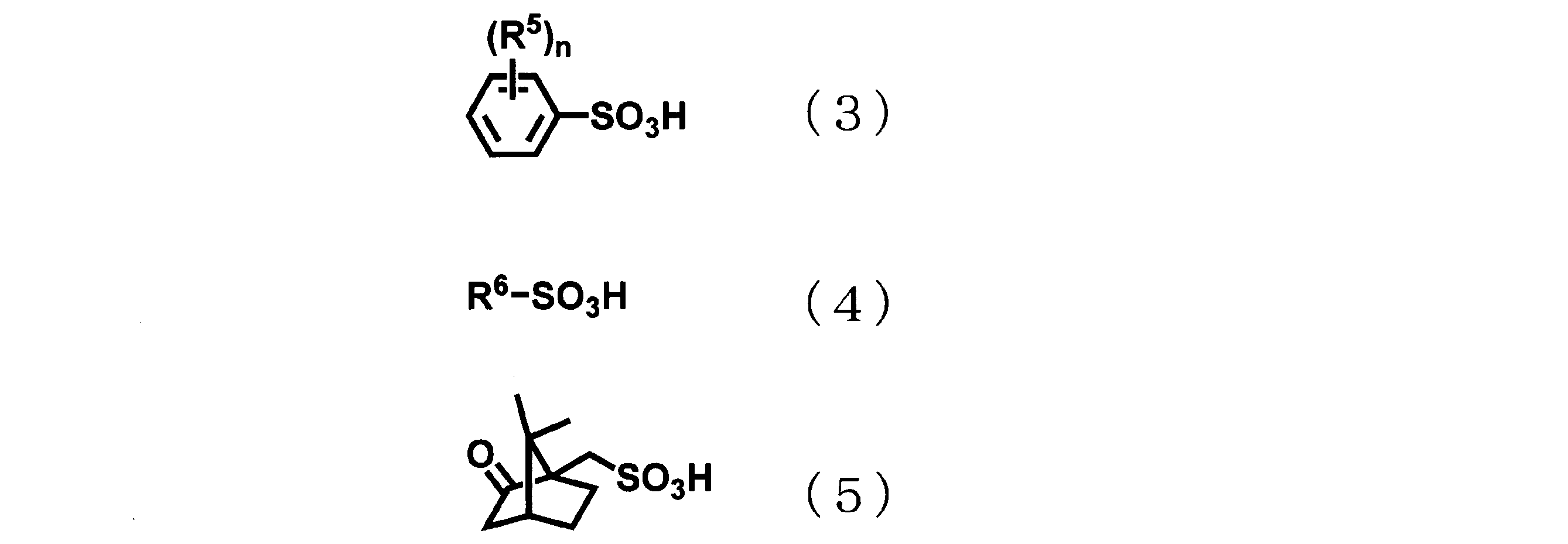
全ての繰り返し単位における酸成分およびアミン成分をそれぞれ100mol%とした場合、酸成分およびアミン成分の合計200mol%のうち、フルオレン構造を有する酸成分およびフルオレン構造を有するアミン成分の合計が0mol%以上50mol%以下である、[1]~[6]のいずれかに記載の硬化膜。



全ての繰り返し単位における酸成分およびアミン成分をそれぞれ100mol%とした場合、酸成分およびアミン成分の合計200mol%のうち、脂環構造を有する酸成分および脂環構造を有するアミン成分の合計が0mol%以上40mol%以下である、[1]~[8]のいずれかに記載の硬化膜。
全ての繰り返し単位における酸成分およびアミン成分をそれぞれ100mol%とした場合、酸成分およびアミン成分の合計200mol%のうち、前記sp2炭素に直接結合しているフッ素原子を有する酸成分および前記sp2炭素に直接結合しているフッ素原子を有するアミン成分の合計が5mol%以上100mol%以下である、[10]に記載の硬化膜。
F/C比が0以上0.05以下であるポリイミド、ポリイミド前駆体、ポリベンゾオキサゾール、ポリベンゾオキサゾール前駆体、およびそれらの共重合体からなる群より選択される1種類以上のポリマーを含む樹脂組成物からなる樹脂膜(以下、樹脂膜1と呼ぶ場合がある。)を形成し、樹脂膜1上にフォトレジストの感光性樹脂膜(以下、感光性樹脂膜1と呼ぶ場合がある。)の形成後、感光性樹脂膜1の露光、感光性樹脂膜1の現像、感光性樹脂膜1のエッチング、感光性樹脂膜1の除去、樹脂膜1の加熱処理をする方法
[方法2]
ポリイミド、ポリイミド前駆体、ポリベンゾオキサゾール、ポリベンゾオキサゾール前駆体、およびそれらの共重合体からなる群より選択される1種類以上のポリマーと、感光性化合物とを含む感光性樹脂組成物であって、該感光性樹脂組成物中から溶剤を除いた固形分中のF/C比が0以上0.05以下であり、該感光性樹脂組成物からなる感光性樹脂膜を形成し、該感光性樹脂膜を露光、現像後に加熱処理する方法。
本発明の硬化膜は、ポリイミドおよび/またはポリベンゾオキサゾール(以下、(a)成分と呼ぶ場合がある。)を含む。本発明の硬化膜が(a)成分を含むことにより、硬化膜の長期信頼性を向上でき、特に有機EL表示装置に用いた場合の高温連続駆動時の発光輝度低下を抑えることができる。


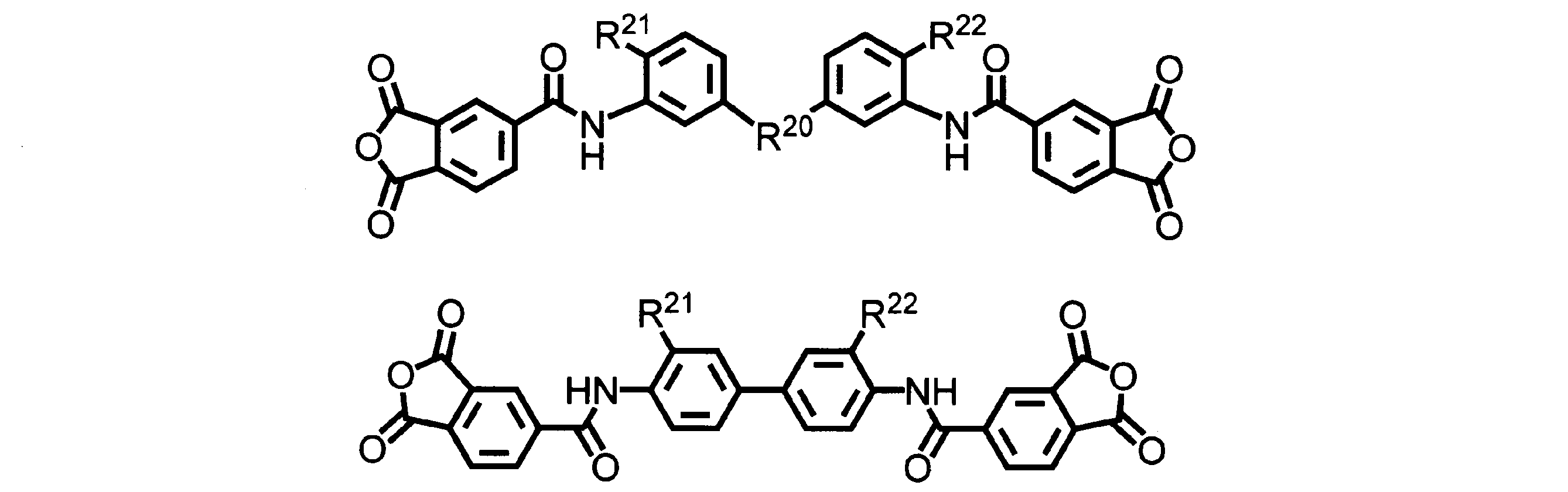
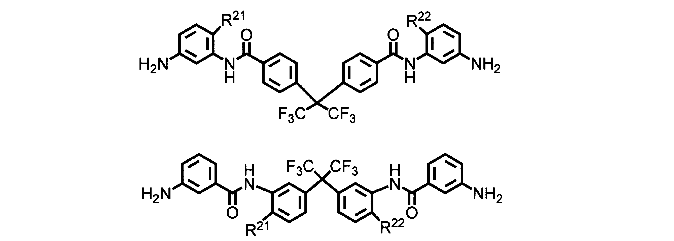


本発明の硬化膜は、1つの芳香環内に少なくとも3つのフェノール性水酸基を有する芳香族炭化水素化合物(以下、(b)成分と呼ぶ場合がある。)を含むことが好ましい。本発明の硬化膜が(b)成分を含むことにより、硬化膜の長期信頼性を向上させ、特に有機EL表示装置に用いた場合の高温連続駆動時の発光輝度低下を抑えることができる。

本発明の硬化膜は、感光性化合物(以下、(c)成分と呼ぶ場合がある。)に由来する化合物を含むことが好ましい。本発明の硬化膜が感光性化合物に由来する化合物を含むことにより、硬化膜の製造工程を簡略化することができる。(c)成分としては、光重合開始剤(以下、(c1)成分と呼ぶ場合がある。)、ナフトキノンジアジド化合物(以下、(c2)成分と呼ぶ場合がある。)などが挙げられる。
本発明の硬化膜は、β-アルコキシプロピオンアミドを含むことが好ましい。本発明の硬化膜がβ-アルコキシプロピオンアミドを含むことにより、硬化膜の長期信頼性を向上させ、特に有機EL表示装置に用いた場合の高温連続駆動時の発光輝度低下を抑えることができる。
本発明の硬化膜は、式(3)~式(5)のいずれかで表される群から選ばれる1種類以上のスルホン酸、または、該スルホン酸に由来するスルホン酸イオン(以下、特定のスルホン酸および/またはスルホン酸イオンと呼ぶ場合がある。)を含むことが好ましい。
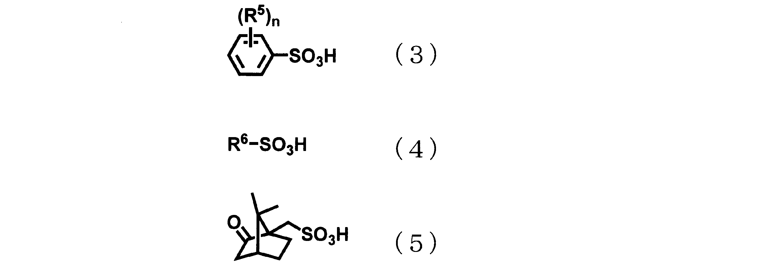
本発明の硬化膜は、さらに着色剤(d)(以下、(d)成分と呼ぶ場合がある。)を含有することが好ましい。本発明の硬化膜が(d)成分を含有することにより、硬化膜の遮光性を向上させ、表示装置に用いた場合の外光反射を抑制させることができる。また、本発明の硬化膜が(d)成分を含有することにより、波長450nmにおける光の透過率を下げ、酸化物半導体TFTを有する有機EL表示装置に本発明の硬化膜を用いた場合において、TFTへの紫外光の進入による誤作動などを防ぐことができる。硬化膜の可視光遮光性を向上させ、膜厚1μm当たりの可視光におけるOD値を向上させる観点から、(d)成分は波長300nm以上850nm以下の範囲のいずれかに最大吸収波長を有することが好ましい。また、波長450nmの光の透過率を30%以下とする観点から、(d)成分は300nm以上600nm以下の範囲のいずれかに最大吸収波長を有することが好ましく、400nm以上500nm以下の範囲のいずれかに最大吸収波長を有することがさらに好ましい。
本発明の硬化膜は、熱架橋剤に由来する化合物を含有してもよい。熱架橋剤とは、アルコキシメチル基、メチロール基、エポキシ基、オキセタニル基などの熱反応性の官能基を分子内に少なくとも2つ有する化合物を指す。本発明の硬化膜が、熱架橋剤に由来する化合物を含有することにより、熱架橋剤と(a)成分との間、または熱架橋剤同士で架橋し、硬化膜の耐熱性、耐薬品性および折り曲げ耐性を向上させることができる。前述の(b)成分と併用した際に、硬化後の300nm~500nmの光の透過率を下げる観点から、熱架橋剤としてアルコキシメチル基またはメチロール基が好ましく、窒素原子に直接置換したアルコキシメチル基またはメチロール基を有することがより好ましい。前述の(b)成分と併用した際に、硬化後の300nm~500nmの光の透過率を下げる観点から、熱架橋剤に由来する化合物は、トリアジン環を有することが好ましい。
本発明の硬化膜は、密着改良剤に由来する化合物を含有してもよい。密着改良剤に由来する化合物としては、公知のシランカップリング剤、チタンキレート剤、アルミキレート剤、芳香族アミン化合物とアルコキシ基含有ケイ素化合物を反応させて得られる化合物に由来する化合物などを含有することができる。これらを2種以上含有してもよい。これらの密着改良剤に由来する化合物を含有することにより、硬化膜のシリコンウエハ、酸化インジウムスズ(ITO)、SiO2、窒化ケイ素、ポリイミドフィルム基板などの下地基材との密着性を高めることができる。
本発明の硬化膜は、無機粒子を含有してもよい。無機粒子の好ましい具体例としては、例えば、酸化珪素、酸化チタン、チタン酸バリウム、アルミナ、タルクなどからなる粒子を挙げることができる。無機粒子の一次粒子径は100nm以下が好ましく、60nm以下がより好ましい。
本発明の硬化膜の製造方法について、基板上に、感光性樹脂組成物からなる感光性樹脂膜を形成し、該感光性樹脂膜を露光および現像した後に加熱処理する方法を例に説明する。
塗布後または減圧乾燥後、得られた塗布膜を加熱乾燥することが一般的である。この工程をプリベークとも言う。乾燥にはホットプレート、オーブン、赤外線などを使用する。ホットプレートを用いる場合、プレート上に直接、もしくは、プレート上に設置したプロキシピン等の治具上に塗布膜を保持して加熱する。加熱時間は1分間~数時間が好ましい。加熱温度は塗布膜の種類や目的により様々であるが、プリベーク時の溶剤乾燥を促進する観点から、80℃以上が好ましく、90℃以上がさらに好ましい。一方、プリベーク時の硬化進行を低減する観点から加熱温度は150℃以下が好ましく、140℃以下がさらに好ましい。
本発明の硬化膜は、半導体素子の表面保護層や層間絶縁層、有機EL素子の画素分割層、有機EL素子を用いた表示装置のTFT基板の平坦化層、回路基板の配線保護絶縁層、固体撮像素子のオンチップマイクロレンズや各種表示装置・固体撮像素子用平坦化層などに好適に用いられる。例えば、耐熱性の低いMRAM、次世代メモリとして有望なポリマーメモリ(Polymer Ferroelectric RAM:PFRAM)や相変化メモリ(Phase Change RAM:PCRAM、Ovonics Unified Memory:OUM)などの表面保護層や層間絶縁層として好適である。
本発明の有機EL表示装置は本発明の硬化膜を有する。本発明の硬化膜を用いた有機EL表示装置は、少なくとも基板、第一電極、第二電極、有機EL層、平坦化層および画素分割層を具備し、前記硬化膜が平坦化層および/または画素分割層に含まれることが好ましい。平坦化層および/または画素分割層に本発明の硬化膜が含まれることで、長期信頼性に優れた有機EL表示装置を提供することが可能となる。
本発明の硬化膜を有する他の態様の表示装置について図2を例として説明する。この表示装置は、少なくとも金属配線、本発明の硬化膜、および複数の発光素子を有する表示装置であって、前記発光素子はいずれか一方の面に一対の電極端子を具備し、前記一対の電極端子は前記硬化膜中に延在する複数本の前記金属配線と接続し、複数本の前記金属配線は、前記硬化膜により電気的絶縁性を保持する構成である。
本発明の電子部品は、本発明の硬化膜を有する電子部品である。本発明の硬化膜は、半導体装置等の電子部品に使用することができる。ここで、電子部品としては、トランジスタ、ダイオード、集積回路(IC)、メモリなどの半導体を有する能動部品、抵抗、キャパシタ、インダクタなどの受動部品が挙げられる。また、半導体を用いた電子部品を半導体装置または半導体パッケージとも称する。本発明でいう半導体装置とは、半導体素子の特性を利用することで機能し得る装置全般を指す。半導体素子を基板に接続した電気光学装置や半導体回路基板、複数の半導体素子を積層したもの、並びにこれらを含む電子装置は、全て半導体装置に含まれる。また、半導体素子を基板に接続するためのインターポーザー等の電子部品も半導体装置に含める。具体的には、本発明の硬化膜は、電気絶縁性、機械強度、接着性、および耐熱性に優れるので、これらが半導体素子のパッシベーション膜やバッファーコート膜といった表面保護膜、半導体素子表面に形成された再配線間の層間絶縁膜、複数の半導体素子を接合した際の素子間の絶縁膜、高密度実装用多層配線基板やインターポーザーの配線層間の絶縁膜として用いることができる。
5センチ角のガラス基板上に各実施例および比較例により得られたワニスを加熱処理(キュア)後の膜厚が2.0μmとなるようにスピンコートで塗布し、120℃で120秒間プリベークし、プリベーク膜を作製した。その後、UV露光はせずに、2.38%水酸化テトラメチルアンモニウム(以下、TMAH)水溶液で未露光部の膜減りが約0.5μmとなるように現像した。次いで、光洋サーモシステム(株)製高温クリーンオーブンINH-9CD-Sを用いて、窒素雰囲気下で250℃60分間キュアし、硬化膜を作製した。
(1)と同様にして作製した現像後の樹脂膜付きガラス基板を、プロピレングリコールモノメチルエーテル中に浸漬し、室温で30分間放置した。その後、ガラス基板をプロピレングリコールモノメチルエーテルから取り出し、ガラス基板上の残渣の有無を目視にて観察し、ガラス基板上に残渣が全く認められない場合は「A」、ガラス基板上に残渣がわずかに認められる場合は「B」、ガラス基板上に残渣が多く認められる場合は「C」と判定した。
ポリイミドフィルム基板上に各実施例および比較例により得られたワニスを加熱処理(キュア)後の膜厚が2.0μmとなるようにスピンコートで塗布し、120℃で120秒間プリベークし、プリベーク膜を作製した。その後、UV露光はせずに、2.38%TMAH水溶液で未露光部の膜減りが約0.5μmとなるように現像した。次いで、光洋サーモシステム(株)製高温クリーンオーブンINH-9CD-Sを用いて、窒素雰囲気下で250℃60分間キュアし、硬化膜を作製した。
(1)と同様の方法で作製した硬化膜を10mg採取し、パージ・アンド・トラップ法にてβ-アルコキシプロピオンアミドを含む成分を吸着捕集した。具体的には、採取した硬化膜をパージガスとしてヘリウムを用いて400℃で60分間加熱し、硬化膜から脱離した成分を吸着管に捕集した。捕集した成分を320℃で5分間加熱して吸着管から脱離させ、GC-MS装置7890/5975C(Agilent社製)を用い、カラム温度:40~300℃、キャリアガス:ヘリウム(1.5mL/min)、スキャン範囲:m/Z29~600の条件で、GC-MS分析を実施した。検出されたβ-アルコキシプロピオンアミドと同じβ-アルコキシプロピオンアミドを標準物質として上記と同一条件でGC-MS分析して検量線を作成することで、β-アルコキシプロピオンアミドのガス発生量を算出した。このように求めたβ-アルコキシプロピオンアミドガス発生量と測定に用いたサンプル質量から硬化膜中のβ-アルコキシプロピオンアミドの含有量(質量%)を算出した。
有機EL表示装置の作製手順の概略図を図3に示す。まず、38mm×46mmの無アルカリガラス基板21に、ITO透明導電膜10nmをスパッタ法により基板全面に形成した後、所望の形状にエッチングして第一電極(透明電極)22を形成した。また同時に、第二電極を取り出すための補助電極23も形成した(図3(1))。得られた電極付き基板をセミコクリーン56(商品名、フルウチ化学(株)製)で10分間超音波洗浄してから、超純水で洗浄した。次にこの基板全面に、各実施例および比較例で得られた感光性樹脂組成物をスピンコート法により塗布し、120℃のホットプレート上で2分間プリベークした。得られたプリベーク膜を、所望のパターンを有するフォトマスクを介して高圧水銀灯を光源として各感光性樹脂組成物の最小露光量で露光した後、2.38質量%TMAH水溶液で現像し、不要な部分を溶解させ、純水でリンスし、樹脂パターンを得た。得られた樹脂パターンを、光洋サーモシステム(株)製高温クリーンオーブンINH-9CD-Sを用いて、大気雰囲気下または窒素雰囲気下で230℃60分間加熱処理し、硬化させた。このようにして、幅70μm、長さ260μmの開口部が幅方向にピッチ155μm、長さ方向にピッチ465μmで配置され、それぞれの開口部が第一電極を露出せしめる形状の画素分割層24を、基板有効エリアに限定して形成した。このようにして、1辺が16mmの四角形である基板有効エリアに開口率25%の画素分割層を形成した。画素分割層の厚さは約1.5μmであった(図3(2))。
(1)と同様の方法で作製した硬化膜について、紫外可視分光光度計MultiSpec-1500(島津製作所(株)製)を用いて波長300nm~800nmの光の透過スペクトルを測定し、キュア後の膜厚2.0μmにおける波長450nmの光の透過率を求めた。
(1)と同様にして作製した硬化膜について、光学濃度計(361T;X-Rite社製)を用いてOD値を測定した。得られたOD値を硬化膜の膜厚で割り返すことで、1μm当たりOD値(以降OD/μmと呼ぶ)を求めた(1μm当たりのOD値=OD値/硬化膜の膜厚)。
乾燥窒素気流下、TrisP-PA(商品名、本州化学工業(株)製)21.22g(0.05モル)と5-ナフトキノンジアジドスルホニル酸クロリド26.87g(0.10モル)を1,4-ジオキサン450gに室温で溶解させた。ここに、1,4-ジオキサン50gと混合したトリエチルアミン15.18gを、系内が35℃以上にならないように滴下した。滴下後30℃で2時間撹拌した。トリエチルアミン塩を濾過して除き、得られたろ液を水に投入し、析出した沈殿をろ過で集めた。得られた沈殿を真空乾燥機で乾燥させ、下記式で表されるキノンジアジド化合物(c-1)を得た。

テトラヒドロフラン2400gに、開始剤としてsec-ブチルリチウム2.56g(0.04モル)を加えた混合液に、p-t-ブトキシスチレン105.75g(0.6モル)を加えて、3時間撹拌しながら重合させた後、メタノール12.82g(0.4モル)を添加して重合停止反応を行った。次にポリマーを精製するために反応混合物をメタノール3L中に注ぎ、沈降したポリマーを乾燥させた。得られたポリマーをアセトン1.6Lに溶解し、60℃で濃塩酸2g加えて7時間撹拌し、p-t-ブトキシ基を脱保護して、p-t-ブトキシスチレンをヒドロキシスチレンに変換した。反応終了後、溶液を水に注いでポリマーを沈殿させ、得られた沈殿物を水で3回洗浄した後、50℃の真空乾燥機で24時間乾燥し、目的のポリヒドロキシスチレン(p-1)を得た。
6FAP18.3g(0.05モル)をアセトン100mLおよびプロピレンオキシド17.4g(0.3モル)に溶解させ、-15℃に冷却した。ここに3-ニトロベンゾイルクロリド20.4g(0.11モル)をアセトン100mLに溶解させた溶液を滴下した。滴下終了後、-15℃で4時間反応させ、その後室温に戻した。析出した白色固体をろ別し、50℃で真空乾燥した。

攪拌機、熱電対および滴下ロートを備えた容量500mlの四ツ口フラスコに、4,4’-(2-エチルヘキシリデン)ジフェノール)を25.66g (0.086モル)および氷酢酸100mlを仕込んで攪拌し、湯浴で内温を50℃まで上げた。これに、1時間かけて濃硝酸2ml(0.026モル)を滴下し、その後氷冷して内温を13℃まで下げ、さらに濃硝酸13.3ml(0.149モル)を1時間かけて滴下した。その後、3時間攪拌を続け、析出した黄色結晶を濾過で集め、氷酢酸40mlおよび脱イオン水80mlで順次洗浄し、減圧乾燥してジニトロ体を得た。

6FAPに代えて、合成例4で得られたジアミン化合物(β)を16.4g(0.05モル)用いたこと以外は合成例3と同様にして、ジアミン化合物(γ)を得た。
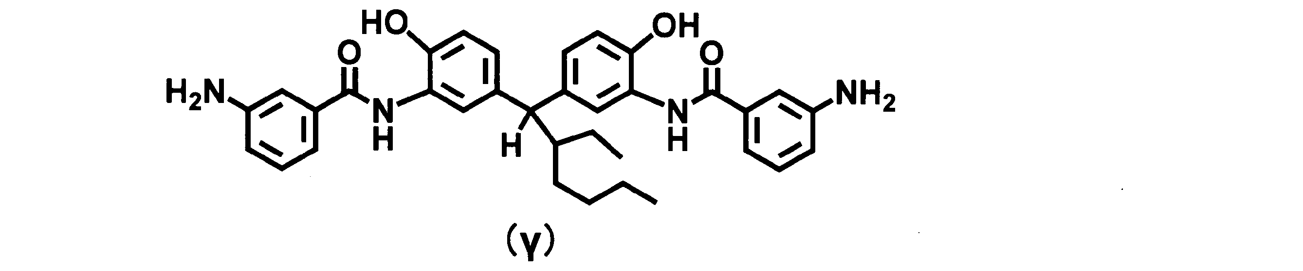
4,4’-(2-エチルヘキシリデン)ジフェノール)に代えて4,4’-(3,3,5-トリメチルシクロへキシリデン)ビスフェノール)を26.70g(0.086モル)用いてジニトロ体を合成し、ジニトロ体を54.06g(0.135モル)用いたこと以外は合成例4と同様にして、ジアミン化合物(δ)を得た。

乾燥窒素気流下、ODPA31.02g(0.10モル)をMPA500gに溶解させた。ここにBAP21.96g(0.085モル)とSiDA1.24g(0.005モル)をMPA50gとともに加えて、40℃で2時間反応させた。次に末端封止剤として3-アミノフェノール2.18g(0.02モル)をMPA5gとともに加え、50℃で2時間反応させた。その後、N,N-ジメチルホルムアミドジエチルアセタール32.39g(0.22モル)をMPA50gで希釈した溶液を投入した。投入後、50℃で3時間撹拌した。撹拌終了後、溶液を室温まで冷却した後、溶液を水3Lに投入して白色沈殿を得た。得られた沈殿を濾過で集めて、水で3回洗浄した後、80℃の真空乾燥機で24時間乾燥し、アルカリ可溶性樹脂であるポリイミド前駆体(a-1)を得た。
乾燥窒素気流下、BAP12.92g(0.050モル)、6FAP12.82g(0.035モル)、SiDA1.24g(0.005モル)、MAP2.18g(0.02モル)、グリシジルメチルエーテル52.8g(0.6モル)をMPA500gに溶解させ、溶液の温度を-15℃まで冷却した。ここにOBBC29.51g(0.10モル)をMPA50gに溶解させた溶液を内部の温度が0℃を越えないように滴下した。滴下終了後、-15℃で6時間撹拌を続けた。反応終了後、メタノールを10重量%含んだ水3Lに溶液を投入して白色の沈殿を集めた。得られた沈殿を濾過で集めて、水で3回洗浄した後、80℃の真空乾燥機で24時間乾燥し、アルカリ可溶性樹脂であるポリベンゾオキサゾール前駆体(a-11)を得た。
アミン成分、酸成分および重合溶剤を表1に記載の通り変更した以外は合成例7と同様にしてポリイミド前駆体(a-2)~(a-10)、(a-12)~(a-19)、(a’-1)~(a’-4)を得た。
アミン成分、酸成分および重合溶剤を表1に記載の通り変更した以外は合成例17と同様にしてポリベンゾオキサゾール前駆体(a’-5)を得た。
GBL:γ-ブチロラクトン
MPA:3-メトキシ-N,N-ジメチルプロパンアミド
NMP:N-メチルピロリドン
BAP:2,2-ビス(3-アミノ-4-ヒドロキシフェニル)プロパン(フッ素原子を含まないジアミン)
ABPS:ビス(3-アミノ-4-ヒドロキシフェニル)スルホン(フッ素原子を含まないジアミン)
BAHF:9,9-ビス(3-アミノ-4-ヒドロキシフェニル)フルオレン(フッ素原子を含まず、フルオレン構造を有するジアミン)
SiDA:1,3-ビス(3-アミノプロピル)テトラメチルジシロキサン(フッ素原子を含まず、ケイ素原子を含むジアミン)
6FAP:2,2-ビス(3-アミノ-4-ヒドロキシフェニル)ヘキサフルオロプロパン(フッ素原子を含むジアミン)
8FBZ:4,4’-ジアミノオクタフルオロビフェニル(sp2炭素に直接結合しているフッ素原子を含むジアミン)
MAP:3-アミノフェノール
ODPA:3,3’,4,4’-ジフェニルエーテルテトラカルボン酸二無水物(フッ素原子を含まない酸二無水物)
TDA:テトラリン二無水物(フッ素原子を含まず、脂環構造を含む酸二無水物)
6FDA:2,2-ビス(3,4-ジカルボキシフェニル)ヘキサフルオロプロパン二無水物(フッ素原子を含む酸二無水物)
OBBC:ジフェニルエーテルジカルボン酸ジクロリド(フッ素原子を含まない酸クロリド)
b-1:1,2,4-トリヒドロキシベンゼン(1つの芳香環内に少なくとも3つのフェノール性水酸基を有する芳香族炭化水素化合物)
b’-1:1,1,1-トリス(4-ヒドロキシフェニル)エタン
BTS:p-トルエンスルホン酸ブチル(加熱処理中に特定のスルホン酸および/またはスルホン酸イオンが発生する熱酸発生剤)
s-1:3-グリシドキシプロピルトリメトキシシラン(シランカップリング剤)
e-1:下記に示した構造で表される熱架橋剤
e-2:下記に示した構造で表される熱架橋剤
d1-1:下記に示した構造で表される染料
d1-2:下記に示した構造で表される染料
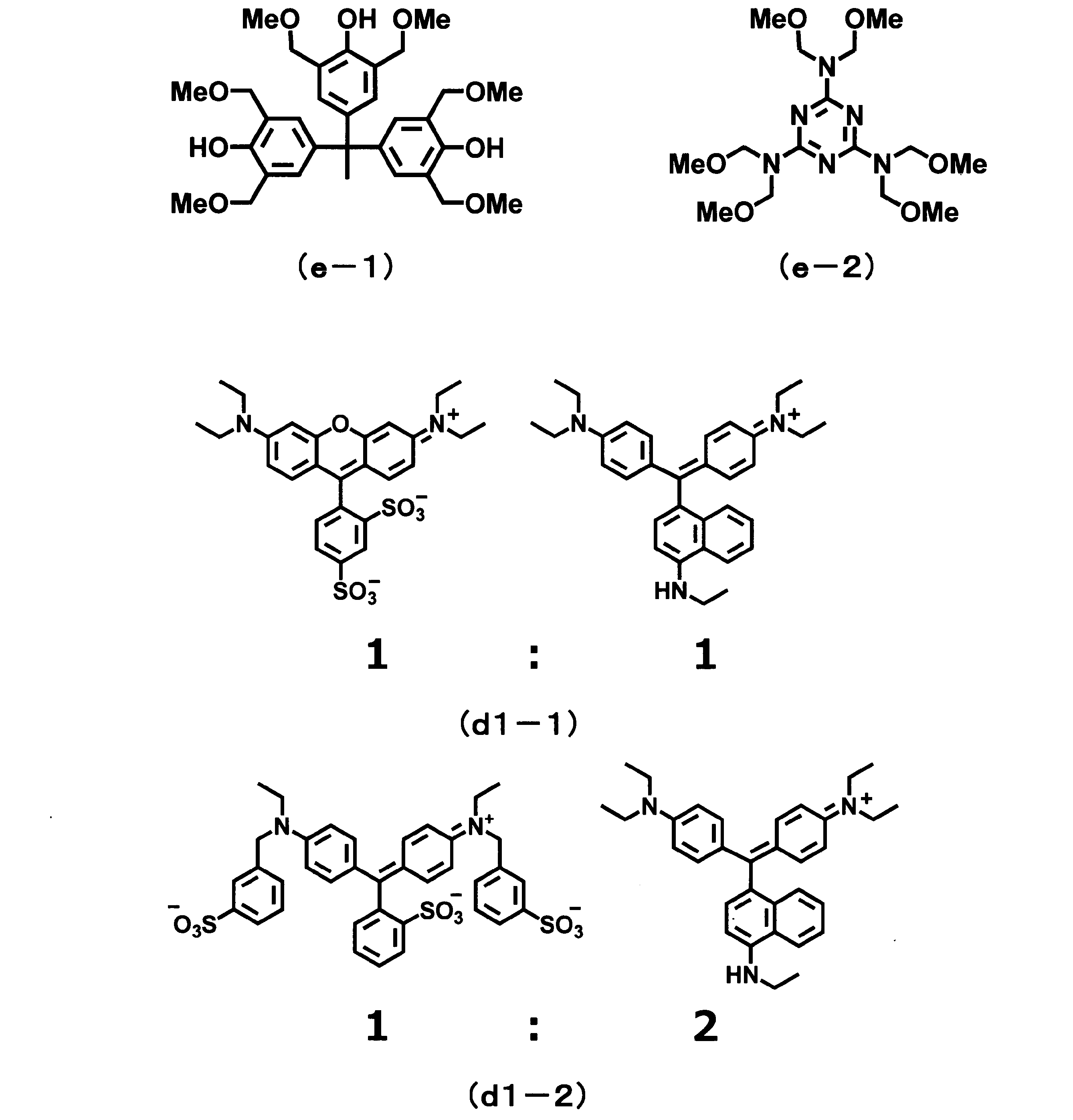
ポリイミド前駆体(a-1)10.0g、感光性化合物(c-1)2.0g、(e-1)2.0gをGBL50gに溶解した後、0.2μmのポリテトラフルオロエチレン製のフィルターでろ過し、ポジ型感光性樹脂組成物のワニスA-1を得た。得られたワニスA-1を用いて前記のように硬化膜の電子線マイクロアナライザ測定、硬化膜作製時のリワーク性評価、硬化膜の折り曲げ耐性評価、硬化膜中のβ-アルコキシプロピオンアミドの含有量の算出、有機EL表示装置の長期信頼性評価、450nmの遮光性の評価および可視光遮光性の評価を行った。
(a)成分、(b)成分、(c)成分、その他成分および溶剤を表2~3に記載の通り変更した以外は実施例1と同様にし、感光性樹脂組成物のワニスを得た。得られたワニスを用いて前記のように硬化膜の電子線マイクロアナライザ測定、硬化膜作製時のリワーク性評価、硬化膜の折り曲げ耐性評価、硬化膜中のβ-アルコキシプロピオンアミドの含有量の算出、有機EL表示装置の長期信頼性評価、450nmの遮光性の評価および可視光遮光性の評価を行った。硬化膜中のキノンジアジド化合物(c-1)に由来する化合物については、実施例1と同様である。

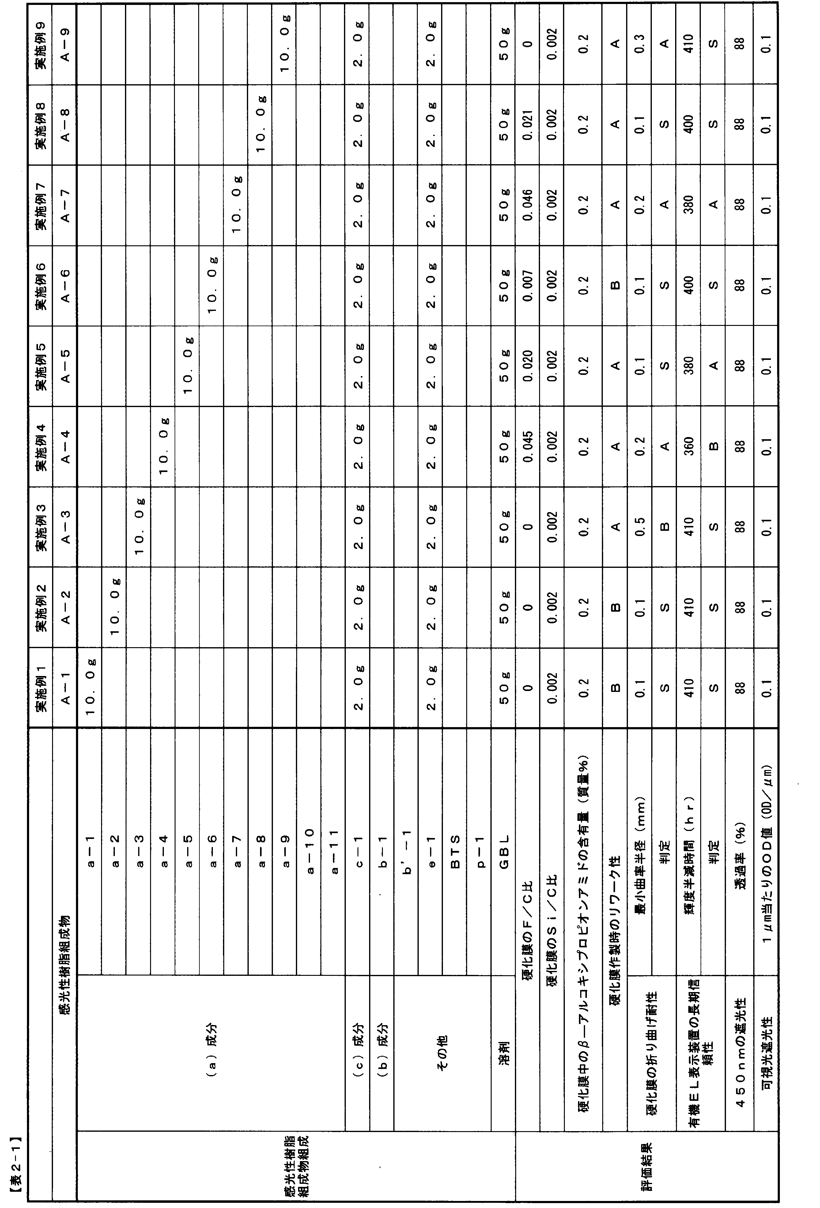
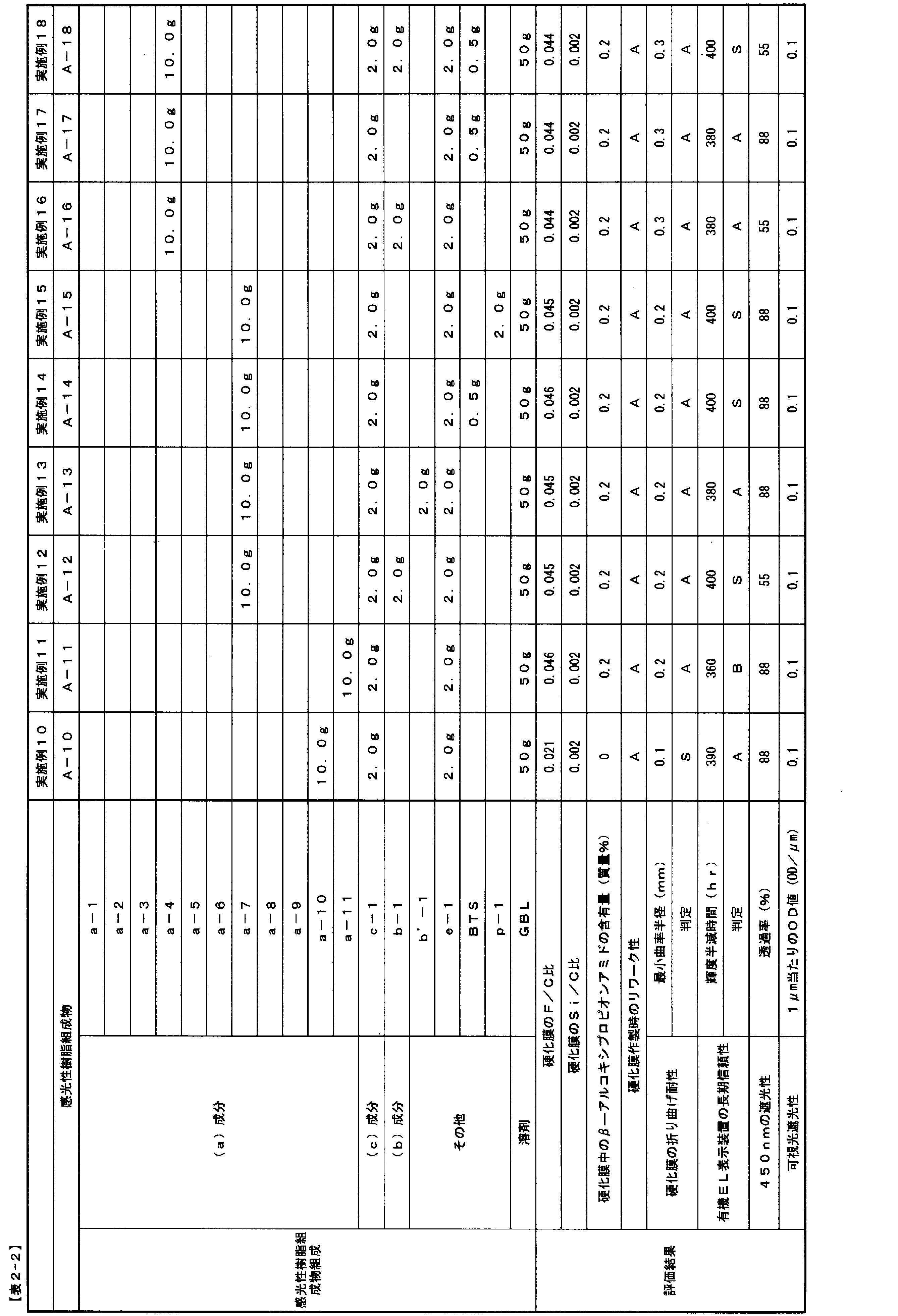
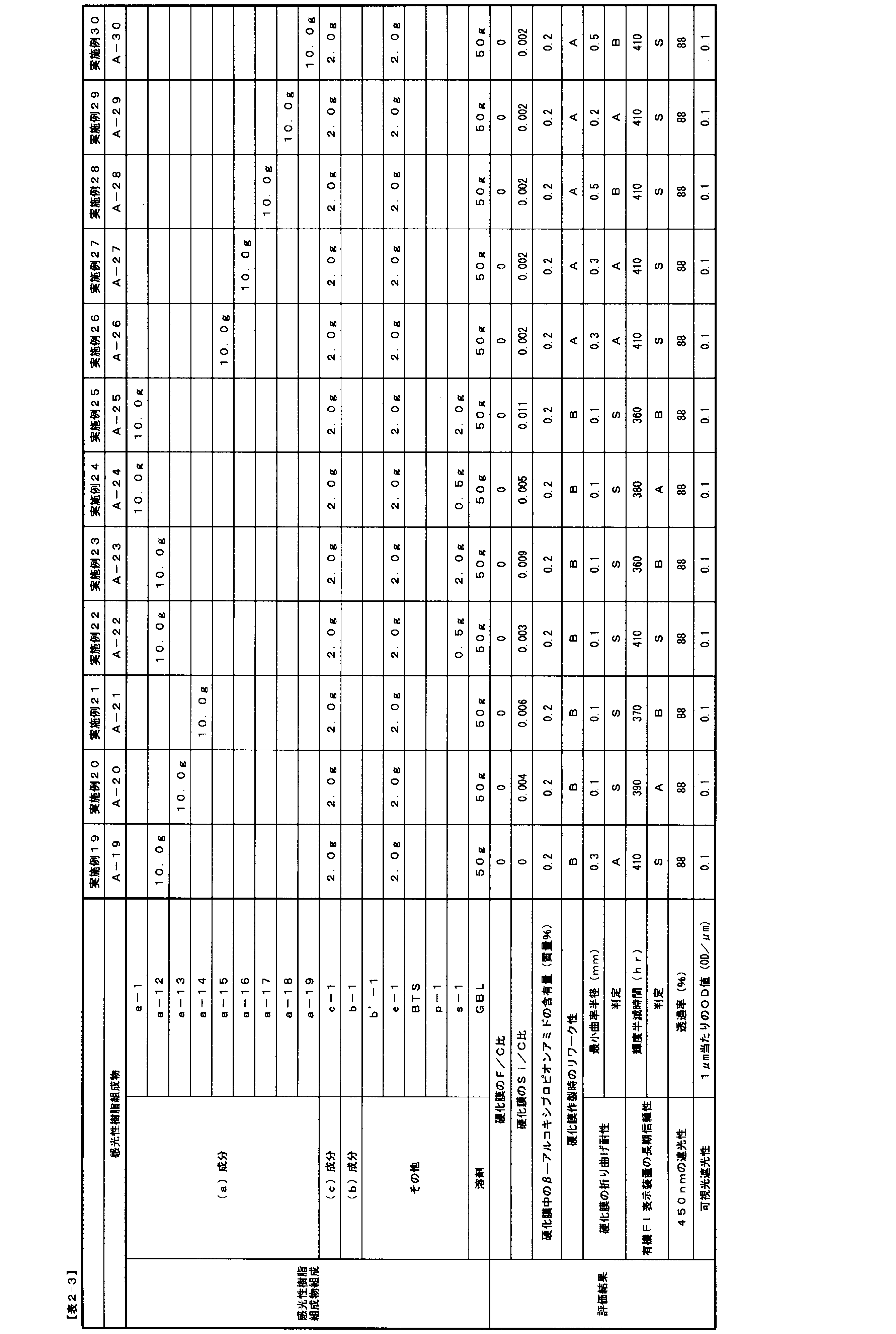

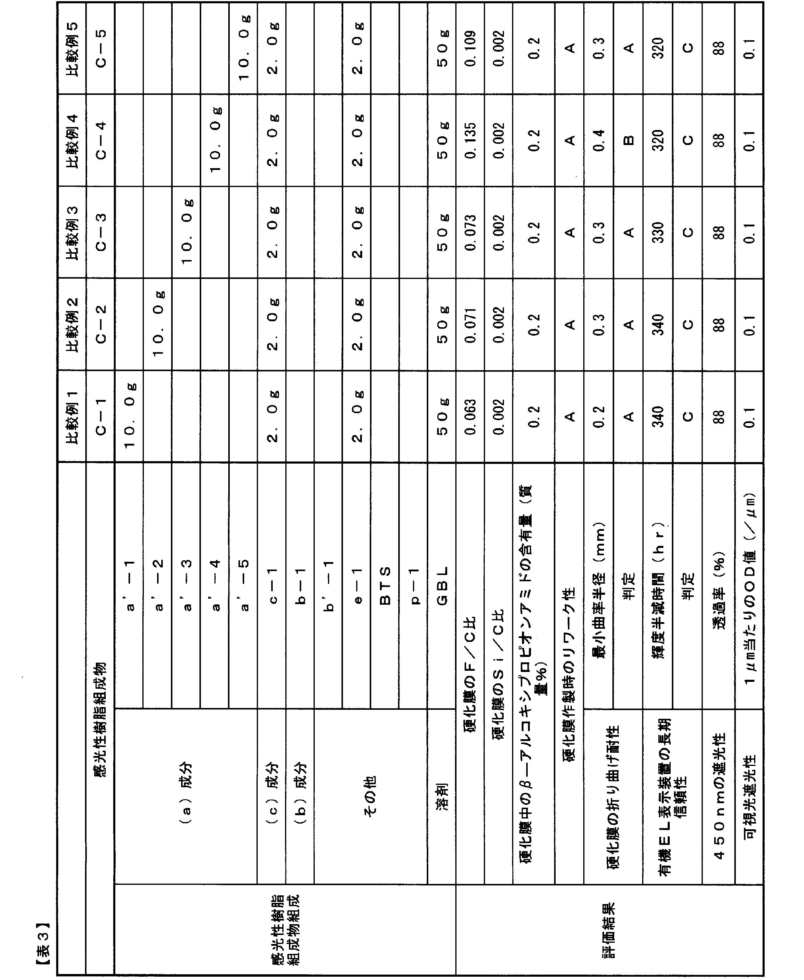
2:TFT
3:TFT絶縁層
4:配線
5:平坦化層
6:コンタクトホール
7:第一電極
8:画素分割層
9:有機EL層
10:第二電極
11:表示装置
12:発光素子
13:硬化膜
14、14c:金属配線
15:対向基板
16:電極端子
17:発光素子駆動基板
18:駆動素子
19:バリアメタル
20:はんだバンプ
21:無アルカリガラス基板
22:第一電極(透明電極)
23:補助電極
24:画素分割層
25:有機EL層
26:第二電極(非透明電極)
Claims (17)
- ポリイミドおよび/またはポリベンゾオキサゾールを含む硬化膜であって、
該硬化膜の断面を電子線マイクロアナライザで測定した際に得られるフッ素原子と炭素原子のモル比F(フッ素原子)/C(炭素原子)が0以上0.05以下である硬化膜。 - さらにインデン構造を含むカルボン酸、インデン構造を含むカルボン酸エステル、インデン構造を含むスルホン酸、およびインデン構造を含むスルホン酸アリールエステルからなる群より選ばれる1種類以上の化合物を含む、請求項1に記載の硬化膜。
- さらにポリヒドロキシスチレン、および/または、ポリヒドロキシスチレン/ポリスチレン共重合体を有する、請求項1または2に記載の硬化膜。
- さらに1つの芳香環内に少なくとも3つのフェノール性水酸基を有する芳香族炭化水素化合物を有する、請求項1または2に記載の硬化膜。
- さらにβ-アルコキシプロピオンアミドを含有する、請求項1または2に記載の硬化膜。
- さらに式(3)~式(5)のいずれかで表される化合物からなる群より選択される1種類以上のスルホン酸、または、式(3)~式(5)のいずれかで表される化合物からなる群より選択される1種類以上のスルホン酸に由来するスルホン酸イオンを有する、請求項1または2に記載の硬化膜:
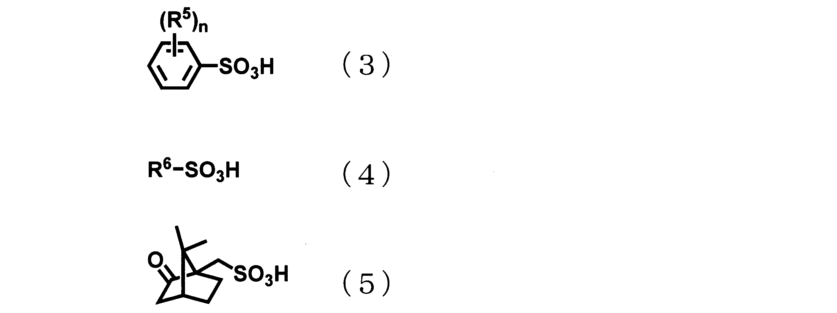
- 前記ポリイミドおよび/またはポリベンゾオキサゾールが、酸成分とアミン成分からなる繰り返し単位を有し、
全ての繰り返し単位における酸成分およびアミン成分をそれぞれ100mol%とした場合、酸成分およびアミン成分の合計200mol%のうち、フルオレン構造を有する酸成分およびフルオレン構造を有するアミン成分の合計が0mol%以上50mol%以下である、請求項1または2に記載の硬化膜。 - 前記ポリイミドおよび/またはポリベンゾオキサゾールが式(6)で表される残基を有する、請求項1または2に記載の硬化膜:



- 前記ポリイミドおよび/またはポリベンゾオキサゾールが、酸成分とアミン成分からなる繰り返し単位を有し、
全ての繰り返し単位における酸成分およびアミン成分をそれぞれ100mol%とした場合、酸成分およびアミン成分の合計200mol%のうち、脂環構造を有する酸成分および脂環構造を有するアミン成分の合計が0mol%以上40mol%以下である、請求項1または2に記載の硬化膜。 - 前記ポリイミドおよび/またはポリベンゾオキサゾールが、sp2炭素に直接結合しているフッ素原子を有する繰り返し単位を含む、請求項1または2に記載の硬化膜。
- 前記ポリイミドおよび/またはポリベンゾオキサゾールが、酸成分とアミン成分からなる繰り返し単位を有し、
全ての繰り返し単位における酸成分およびアミン成分をそれぞれ100mol%とした場合、酸成分およびアミン成分の合計200mol%のうち、前記sp2炭素に直接結合しているフッ素原子を有する酸成分および前記sp2炭素に直接結合しているフッ素原子を有するアミン成分の合計が5mol%以上100mol%以下である、請求項10に記載の硬化膜。 - 前記硬化膜の断面を電子線マイクロアナライザで測定した際に得られるケイ素原子と炭素原子のモル比Si(ケイ素原子)/C(炭素原子)が0.001以上0.005以下である、請求項1または2に記載の硬化膜。
- 膜厚2.0μmにおける波長450nmの光の透過率が30%以下である、請求項1または2に記載の硬化膜。
- 膜厚1μm当たりの可視光におけるOD値が0.5~1.5である、請求項1または2に記載の硬化膜。
- 請求項1または2に記載の硬化膜を有する有機EL表示装置。
- さらにブラックマトリクスを有するカラーフィルタを有する、請求項15に記載の有機EL表示装置。
- 請求項1または2に記載の硬化膜を有する電子部品。
Priority Applications (4)
| Application Number | Priority Date | Filing Date | Title |
|---|---|---|---|
| CN202480033082.1A CN121127518A (zh) | 2023-06-27 | 2024-06-21 | 硬化膜及有机el显示装置 |
| EP24831871.9A EP4737506A1 (en) | 2023-06-27 | 2024-06-21 | Cured film and organic el display device |
| KR1020257041447A KR20260029282A (ko) | 2023-06-27 | 2024-06-21 | 경화막 및 유기 el 표시 장치 |
| JP2024539944A JPWO2025005010A1 (ja) | 2023-06-27 | 2024-06-21 |
Applications Claiming Priority (2)
| Application Number | Priority Date | Filing Date | Title |
|---|---|---|---|
| JP2023-104748 | 2023-06-27 | ||
| JP2023104748 | 2023-06-27 |
Publications (1)
| Publication Number | Publication Date |
|---|---|
| WO2025005010A1 true WO2025005010A1 (ja) | 2025-01-02 |
Family
ID=93938559
Family Applications (1)
| Application Number | Title | Priority Date | Filing Date |
|---|---|---|---|
| PCT/JP2024/022588 Ceased WO2025005010A1 (ja) | 2023-06-27 | 2024-06-21 | 硬化膜、及び有機el表示装置 |
Country Status (6)
| Country | Link |
|---|---|
| EP (1) | EP4737506A1 (ja) |
| JP (1) | JPWO2025005010A1 (ja) |
| KR (1) | KR20260029282A (ja) |
| CN (1) | CN121127518A (ja) |
| TW (1) | TW202500635A (ja) |
| WO (1) | WO2025005010A1 (ja) |
Citations (9)
| Publication number | Priority date | Publication date | Assignee | Title |
|---|---|---|---|---|
| US6252033B1 (en) * | 2000-03-20 | 2001-06-26 | Saehan Industries Incorporation | Method for the preparation of polyamic acid and polymide useful for adhesives |
| JP2002091343A (ja) | 2000-06-28 | 2002-03-27 | Toray Ind Inc | 表示装置 |
| JP2002116715A (ja) | 2000-06-28 | 2002-04-19 | Toray Ind Inc | 表示装置 |
| WO2010010842A1 (ja) * | 2008-07-22 | 2010-01-28 | 住友ベークライト株式会社 | ポジ型感光性樹脂組成物、硬化膜、保護膜、絶縁膜およびそれを用いた半導体装置、表示体装置 |
| WO2016047483A1 (ja) | 2014-09-26 | 2016-03-31 | 東レ株式会社 | 有機el表示装置 |
| JP2019172975A (ja) * | 2018-03-26 | 2019-10-10 | 東レ株式会社 | 樹脂組成物、樹脂シート、硬化膜 |
| JP2022136981A (ja) * | 2021-03-08 | 2022-09-21 | 東レ株式会社 | 感光性組成物、硬化物、表示装置、及び硬化物の製造方法 |
| JP2022137420A (ja) * | 2021-03-09 | 2022-09-22 | 信越化学工業株式会社 | ポリイミドを含む重合体、ポジ型感光性樹脂組成物、ネガ型感光性樹脂組成物、パターン形成方法、硬化被膜形成方法、層間絶縁膜、表面保護膜、及び電子部品 |
| WO2023013550A1 (ja) * | 2021-08-04 | 2023-02-09 | 東レ株式会社 | 化合物、樹脂組成物、硬化物、及び表示装置 |
-
2024
- 2024-06-21 CN CN202480033082.1A patent/CN121127518A/zh active Pending
- 2024-06-21 EP EP24831871.9A patent/EP4737506A1/en active Pending
- 2024-06-21 WO PCT/JP2024/022588 patent/WO2025005010A1/ja not_active Ceased
- 2024-06-21 KR KR1020257041447A patent/KR20260029282A/ko active Pending
- 2024-06-21 JP JP2024539944A patent/JPWO2025005010A1/ja active Pending
- 2024-06-25 TW TW113123570A patent/TW202500635A/zh unknown
Patent Citations (9)
| Publication number | Priority date | Publication date | Assignee | Title |
|---|---|---|---|---|
| US6252033B1 (en) * | 2000-03-20 | 2001-06-26 | Saehan Industries Incorporation | Method for the preparation of polyamic acid and polymide useful for adhesives |
| JP2002091343A (ja) | 2000-06-28 | 2002-03-27 | Toray Ind Inc | 表示装置 |
| JP2002116715A (ja) | 2000-06-28 | 2002-04-19 | Toray Ind Inc | 表示装置 |
| WO2010010842A1 (ja) * | 2008-07-22 | 2010-01-28 | 住友ベークライト株式会社 | ポジ型感光性樹脂組成物、硬化膜、保護膜、絶縁膜およびそれを用いた半導体装置、表示体装置 |
| WO2016047483A1 (ja) | 2014-09-26 | 2016-03-31 | 東レ株式会社 | 有機el表示装置 |
| JP2019172975A (ja) * | 2018-03-26 | 2019-10-10 | 東レ株式会社 | 樹脂組成物、樹脂シート、硬化膜 |
| JP2022136981A (ja) * | 2021-03-08 | 2022-09-21 | 東レ株式会社 | 感光性組成物、硬化物、表示装置、及び硬化物の製造方法 |
| JP2022137420A (ja) * | 2021-03-09 | 2022-09-22 | 信越化学工業株式会社 | ポリイミドを含む重合体、ポジ型感光性樹脂組成物、ネガ型感光性樹脂組成物、パターン形成方法、硬化被膜形成方法、層間絶縁膜、表面保護膜、及び電子部品 |
| WO2023013550A1 (ja) * | 2021-08-04 | 2023-02-09 | 東レ株式会社 | 化合物、樹脂組成物、硬化物、及び表示装置 |
Also Published As
| Publication number | Publication date |
|---|---|
| CN121127518A (zh) | 2025-12-12 |
| JPWO2025005010A1 (ja) | 2025-01-02 |
| TW202500635A (zh) | 2025-01-01 |
| EP4737506A1 (en) | 2026-05-06 |
| KR20260029282A (ko) | 2026-03-04 |
Similar Documents
| Publication | Publication Date | Title |
|---|---|---|
| TWI746650B (zh) | 樹脂組成物、硬化膜、半導體裝置及其等之製造方法 | |
| TWI725250B (zh) | 樹脂組成物、樹脂薄片、硬化膜、有機el顯示裝置、半導體電子零件、半導體裝置及有機el顯示裝置之製造方法 | |
| JP7003659B2 (ja) | 樹脂組成物 | |
| JP6601218B2 (ja) | 樹脂組成物、耐熱性樹脂膜の製造方法、および表示装置 | |
| CN107079560B (zh) | 有机el显示装置 | |
| TWI724137B (zh) | 具備硬化膜之有機 el 顯示元件 | |
| TW201829581A (zh) | 樹脂組成物 | |
| WO2019065351A1 (ja) | 感光性樹脂組成物、硬化膜、硬化膜を具備する素子、硬化膜を具備する有機el表示装置、硬化膜の製造方法、および有機el表示装置の製造方法 | |
| CN118077312B (zh) | 有机el显示装置 | |
| WO2020184326A1 (ja) | 感光性樹脂組成物、感光性樹脂シート、硬化膜、硬化膜の製造方法、有機el表示装置、および電子部品 | |
| JP2008039961A (ja) | ポジ型感光性樹脂組成物およびそれを用いた有機エレクトロルミネッセンス素子 | |
| JP7679918B1 (ja) | 有機el表示装置 | |
| JP2021039295A (ja) | 感光性樹脂組成物、硬化膜、硬化膜を具備する素子および有機el表示装置 | |
| TW202429194A (zh) | 感光性樹脂組成物、硬化物、有機el顯示裝置、顯示裝置、及酚化合物 | |
| TW202500635A (zh) | 硬化膜、有機el顯示裝置及電子零件 | |
| JP6808928B2 (ja) | 感光性樹脂組成物 | |
| TW202330729A (zh) | 感光性樹脂組成物、硬化物、有機el顯示裝置、半導體裝置及硬化物的製造方法 | |
| TW202323342A (zh) | 樹脂組成物、硬化物、有機el顯示裝置及硬化物之製造方法 | |
| WO2025203858A1 (ja) | 感光性樹脂組成物、硬化物、表示装置 | |
| WO2023182327A1 (ja) | ポジ型感光性樹脂組成物、硬化物、有機el表示装置、硬化物の製造方法 | |
| KR20240161633A (ko) | 감광성 수지 조성물, 경화물, 경화물의 제조 방법, 유기 el 표시 장치 및 표시 장치 | |
| WO2025225491A1 (ja) | 感光性樹脂組成物、硬化物、有機el表示装置 |
Legal Events
| Date | Code | Title | Description |
|---|---|---|---|
| WWE | Wipo information: entry into national phase |
Ref document number: 2024539944 Country of ref document: JP |
|
| 121 | Ep: the epo has been informed by wipo that ep was designated in this application |
Ref document number: 24831871 Country of ref document: EP Kind code of ref document: A1 |
|
| WWE | Wipo information: entry into national phase |
Ref document number: 2024831871 Country of ref document: EP |
|
| NENP | Non-entry into the national phase |
Ref country code: DE |
|
| WWE | Wipo information: entry into national phase |
Ref document number: 11202508037R Country of ref document: SG |
|
| WWP | Wipo information: published in national office |
Ref document number: 11202508037R Country of ref document: SG |
|
| ENP | Entry into the national phase |
Ref document number: 2024831871 Country of ref document: EP Effective date: 20260127 |
|
| ENP | Entry into the national phase |
Ref document number: 2024831871 Country of ref document: EP Effective date: 20260127 |
|
| WWP | Wipo information: published in national office |
Ref document number: 2024831871 Country of ref document: EP |