WO2025004806A1 - 配線基板 - Google Patents
配線基板 Download PDFInfo
- Publication number
- WO2025004806A1 WO2025004806A1 PCT/JP2024/021340 JP2024021340W WO2025004806A1 WO 2025004806 A1 WO2025004806 A1 WO 2025004806A1 JP 2024021340 W JP2024021340 W JP 2024021340W WO 2025004806 A1 WO2025004806 A1 WO 2025004806A1
- Authority
- WO
- WIPO (PCT)
- Prior art keywords
- resin
- group
- mass
- compound
- resins
- Prior art date
- Legal status (The legal status is an assumption and is not a legal conclusion. Google has not performed a legal analysis and makes no representation as to the accuracy of the status listed.)
- Ceased
Links
Images




Classifications
-
- H—ELECTRICITY
- H05—ELECTRIC TECHNIQUES NOT OTHERWISE PROVIDED FOR
- H05K—PRINTED CIRCUITS; CASINGS OR CONSTRUCTIONAL DETAILS OF ELECTRIC APPARATUS; MANUFACTURE OF ASSEMBLAGES OF ELECTRICAL COMPONENTS
- H05K1/00—Printed circuits
- H05K1/02—Details
- H05K1/0213—Electrical arrangements not otherwise provided for
- H05K1/0237—High frequency adaptations
- H05K1/0242—Structural details of individual signal conductors, e.g. related to the skin effect
-
- H—ELECTRICITY
- H05—ELECTRIC TECHNIQUES NOT OTHERWISE PROVIDED FOR
- H05K—PRINTED CIRCUITS; CASINGS OR CONSTRUCTIONAL DETAILS OF ELECTRIC APPARATUS; MANUFACTURE OF ASSEMBLAGES OF ELECTRICAL COMPONENTS
- H05K1/00—Printed circuits
- H05K1/02—Details
- H05K1/0213—Electrical arrangements not otherwise provided for
- H05K1/0216—Reduction of cross-talk, noise or electromagnetic interference
- H05K1/023—Reduction of cross-talk, noise or electromagnetic interference using auxiliary mounted passive components or auxiliary substances
- H05K1/0233—Filters, inductors or a magnetic substance
-
- H—ELECTRICITY
- H05—ELECTRIC TECHNIQUES NOT OTHERWISE PROVIDED FOR
- H05K—PRINTED CIRCUITS; CASINGS OR CONSTRUCTIONAL DETAILS OF ELECTRIC APPARATUS; MANUFACTURE OF ASSEMBLAGES OF ELECTRICAL COMPONENTS
- H05K1/00—Printed circuits
- H05K1/02—Details
- H05K1/0213—Electrical arrangements not otherwise provided for
- H05K1/0237—High frequency adaptations
- H05K1/024—Dielectric details, e.g. changing the dielectric material around a transmission line
-
- H—ELECTRICITY
- H05—ELECTRIC TECHNIQUES NOT OTHERWISE PROVIDED FOR
- H05K—PRINTED CIRCUITS; CASINGS OR CONSTRUCTIONAL DETAILS OF ELECTRIC APPARATUS; MANUFACTURE OF ASSEMBLAGES OF ELECTRICAL COMPONENTS
- H05K1/00—Printed circuits
- H05K1/02—Details
- H05K1/0213—Electrical arrangements not otherwise provided for
- H05K1/0237—High frequency adaptations
- H05K1/0245—Lay-out of balanced signal pairs, e.g. differential lines or twisted lines
-
- H—ELECTRICITY
- H05—ELECTRIC TECHNIQUES NOT OTHERWISE PROVIDED FOR
- H05K—PRINTED CIRCUITS; CASINGS OR CONSTRUCTIONAL DETAILS OF ELECTRIC APPARATUS; MANUFACTURE OF ASSEMBLAGES OF ELECTRICAL COMPONENTS
- H05K1/00—Printed circuits
- H05K1/02—Details
- H05K1/0296—Conductive pattern lay-out details not covered by sub groups H05K1/02 - H05K1/0295
- H05K1/0298—Multilayer circuits
-
- H—ELECTRICITY
- H05—ELECTRIC TECHNIQUES NOT OTHERWISE PROVIDED FOR
- H05K—PRINTED CIRCUITS; CASINGS OR CONSTRUCTIONAL DETAILS OF ELECTRIC APPARATUS; MANUFACTURE OF ASSEMBLAGES OF ELECTRICAL COMPONENTS
- H05K1/00—Printed circuits
- H05K1/16—Printed circuits incorporating printed electric components, e.g. printed resistors, capacitors or inductors
- H05K1/165—Printed circuits incorporating printed electric components, e.g. printed resistors, capacitors or inductors incorporating printed inductors
-
- H—ELECTRICITY
- H05—ELECTRIC TECHNIQUES NOT OTHERWISE PROVIDED FOR
- H05K—PRINTED CIRCUITS; CASINGS OR CONSTRUCTIONAL DETAILS OF ELECTRIC APPARATUS; MANUFACTURE OF ASSEMBLAGES OF ELECTRICAL COMPONENTS
- H05K3/00—Apparatus or processes for manufacturing printed circuits
- H05K3/38—Improvement of the adhesion between the insulating substrate and the metal
-
- H—ELECTRICITY
- H05—ELECTRIC TECHNIQUES NOT OTHERWISE PROVIDED FOR
- H05K—PRINTED CIRCUITS; CASINGS OR CONSTRUCTIONAL DETAILS OF ELECTRIC APPARATUS; MANUFACTURE OF ASSEMBLAGES OF ELECTRICAL COMPONENTS
- H05K3/00—Apparatus or processes for manufacturing printed circuits
- H05K3/46—Manufacturing multilayer circuits
-
- H—ELECTRICITY
- H05—ELECTRIC TECHNIQUES NOT OTHERWISE PROVIDED FOR
- H05K—PRINTED CIRCUITS; CASINGS OR CONSTRUCTIONAL DETAILS OF ELECTRIC APPARATUS; MANUFACTURE OF ASSEMBLAGES OF ELECTRICAL COMPONENTS
- H05K2201/00—Indexing scheme relating to printed circuits covered by H05K1/00
- H05K2201/08—Magnetic details
- H05K2201/083—Magnetic materials
- H05K2201/086—Magnetic materials for inductive purposes, e.g. printed inductor with ferrite core
Definitions
- This disclosure relates to a wiring board.
- This disclosure provides a wiring board that can achieve both good adhesion between the conductor wiring and the insulating layer and reduced scattering loss.
- the substrate wiring of the first aspect is A conductor wiring; an insulating layer having a first main surface to which a surface of the conductor wiring is in close contact and a second main surface opposite to the first main surface; a magnetic layer located on the second main surface side of the insulating layer; a conductor layer located on the opposite side of the insulating layer with respect to the magnetic layer,
- the surface or the first main surface has an arithmetic mean roughness of 0.1 ⁇ m or more and 5.0 ⁇ m or less.
- a second aspect is the wiring board of the first aspect,
- the magnetic layer has a thickness of 0.1 ⁇ m or more and 100 ⁇ m or less.
- a third aspect is the wiring board of the first or second aspect,
- the magnetic layer has a relative permeability of 1.5 or more at a frequency of 30 GHz or more.
- a fourth aspect is a wiring board according to any one of the first to third aspects,
- the magnetic layer has a portion that is wider than the conductive wiring.
- a fifth aspect is a wiring board according to any one of the first to fourth aspects,
- the insulating layer has a portion that is the same as or thinner than the thickness of the magnetic layer.
- a sixth aspect is the wiring board according to any one of the first to fifth aspects, A second insulating layer is provided between the magnetic layer and the conductive layer.
- This disclosure makes it possible to provide a wiring board that can achieve both good adhesion between the conductor wiring and the insulating layer and reduced scattering loss.
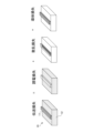
- FIG. 11 is a diagram for explaining a breakdown of transmission loss.
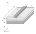
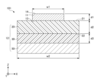
- FIG. 2 is a perspective view showing a configuration example of a wiring board according to the first embodiment; 1 is a cross-sectional view showing a configuration example of a wiring board according to a first embodiment;
- FIG. 13 is a diagram showing an example of a current distribution in a conductor wiring when there is no magnetic layer.
- FIG. 13 is a diagram showing an example of a current distribution in a conductor wiring when a magnetic layer is present.
- FIG. 11 is a cross-sectional view showing a configuration example of a wiring board according to a second embodiment.
- FIG. 1 is a diagram for explaining an example of the concept of a scattering loss evaluation method.
- FIG. 1 is a diagram for explaining an example of the concept of a scattering loss evaluation method.
- FIG. 8 is a simulation diagram showing an example of scattering loss calculated using the evaluation method of FIG. 7 .
- 11 is a table showing an example of calculation results of scattering losses of the wiring board of the first embodiment and a wiring board of a comparative embodiment.
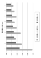
- 5 is a graph showing an example of calculation results of scattering loss of the wiring board of the first embodiment and a wiring board of a comparative embodiment.
- 5 is a graph showing an example of calculation results of scattering loss of the wiring board of the first embodiment and a wiring board of a comparative embodiment.
- 13 is a graph showing an example of calculation results of scattering loss of the wiring board of the second embodiment and a wiring board of a comparative embodiment.
- each part in the drawings may differ from the actual scale.
- Directions such as parallel, right angle, orthogonal, horizontal, vertical, up, down, left, and right are permitted to a degree that does not impair the action and effect of the embodiment.
- the X-axis direction, Y-axis direction, and Z-axis direction respectively represent directions parallel to the X-axis, Y-axis, and Z-axis.
- the X-axis direction, Y-axis direction, and Z-axis direction are mutually perpendicular.
- the XY plane, YZ plane, and ZX plane respectively represent imaginary planes parallel to the X-axis direction and Y-axis direction, imaginary planes parallel to the Y-axis direction and Z-axis direction, and imaginary planes parallel to the Z-axis direction and X-axis direction.
- the term "layer” may include a structure having a shape formed on the entire surface as well as a structure having a shape formed on a part of the surface when observed in a plan view.
- the materials exemplified below may be used alone or in combination of two or more.
- the content of each component in the composition means the total amount of the plurality of substances present in the composition unless otherwise specified.
- a numerical range indicated using “ ⁇ ” indicates a range including the numerical values before and after " ⁇ " as the minimum and maximum values, respectively.
- the upper or lower limit of a numerical range of a certain stage may be replaced by the upper or lower limit of a numerical range of another stage.
- the upper or lower limit of the numerical range may be replaced by the values shown in the examples.
- Transmission loss refers to the degree to which signals such as electrical, optical, or acoustic signals attenuate in a communication path depending on the distance, etc. In the case of a wiring board on which a transmission line such as a microstrip line is formed, the higher the frequency of the signal, the greater the transmission loss.
- Figure 1 is a diagram to explain the breakdown of transmission loss.
- Transmission loss is equal to the sum of dielectric loss, scattering loss, and conductor loss.
- Dielectric loss is a phenomenon in which, when an AC electric field is applied to a dielectric, part of the electrical energy supplied by the AC electric field is lost as heat inside the dielectric. Dielectric loss depends on the dielectric properties of the dielectric. Specifically, the magnitude of dielectric loss varies depending on the dielectric tangent and dielectric constant. The higher the frequency, the greater the dielectric loss, and the greater the dielectric tangent or dielectric constant.
- conductor wiring 11 is formed on or above and below substrate 12, which is a dielectric.
- substrate 12 which is a dielectric.
- Conductor loss refers to the phenomenon in which part of the energy of a signal transmitted through the conductor wiring 11 becomes Joule heat inside the conductor wiring 11 and is lost due to the resistance or skin effect of the conductor wiring 11.
- the current signal is direct current
- the current signal is alternating current
- the higher the frequency of the signal the shallower the skin depth becomes due to the skin effect.
- Skin depth is an index that indicates how far below the surface of the conductor the current flows. The shallower the skin depth, the higher the resistance of the conductor wiring 11 becomes for an AC signal. For this reason, when an AC current signal is transmitted through the conductor wiring 11, the higher the frequency of the signal, the greater the conductor loss.
- Scattering loss refers to the phenomenon in which, when a high-frequency electric field is applied to the conductor wiring 11, the signal transmitted through the conductor wiring 11 is scattered and lost as heat due to roughened areas on the surface of the conductor wiring 11 or on the interface between the conductor wiring 11 and the substrate 12.
- a roughened area refers to an uneven area on the surface or interface.
- the surface of conductor wiring 11 or the interface between conductor wiring 11 and substrate 12 is often roughened to improve adhesion between conductor wiring 11 and substrate 12.
- the higher the frequency band of the signal the greater the skin effect. Therefore, scattering due to the roughened parts of the surface of conductor wiring 11 or the interface between conductor wiring 11 and substrate 12 can be a major factor affecting transmission loss.
- FIG. 2 is a perspective view showing an example of the configuration of the wiring board of the first embodiment.
- Fig. 3 is a cross-sectional view showing an example of the configuration of the wiring board of the first embodiment.
- Figs. 2 and 3 may show an example of the configuration in which a part of the wiring board of the first embodiment is cut out. This also applies to the drawings showing other embodiments described later.
- the first embodiment will be described with reference to Figs. 2 and 3.
- the wiring board 101 shown in Figures 2 and 3 includes a substrate 12 and conductor wiring 11.
- the substrate 12 includes an insulating layer 20, a magnetic layer 30, and a conductor layer 50.
- the conductor wiring 11 is a conductive signal line extending in the Y-axis direction.
- the conductor wiring 11 has an input end 15 facing the negative Y-axis direction, an output end 16 facing the positive Y-axis direction, an upper surface 14 facing the positive Z-axis direction, and a lower surface 13 facing the negative Z-axis direction.
- the lower surface 13 is a surface that is in close contact with the first main surface 21 of the insulating layer 20.
- the high-frequency current signal transmitted through the conductor wiring 11 flows from the input end 15 to the output end 16.
- the conductor wiring 11 has a wiring length L in the Y-axis direction from the input end 15 to the output end 16, a wiring width w1 in the X-axis direction from one side to the other side, and a wiring thickness d1 in the Z-axis direction from the bottom surface 13 to the top surface 14.
- the conductor wiring 11 is a signal line of a transmission line formed on the wiring board 101.
- Examples of the transmission line include a microstrip line, a coplanar line, and a strip line.
- the conductor layer 50 functions as a ground pattern of the transmission line.
- the conductor wiring 11 is formed of a conductive metal such as copper.
- the insulating layer 20 is an insulator that extends along the XY plane.
- the insulating layer 20 has a first main surface 21 that faces the positive Z-axis direction and a second main surface 22 that faces the negative Z-axis direction.
- the second main surface 22 is the surface opposite the first main surface 21 in the Z-axis direction.
- the insulating layer 20 has a width w2 along the X-axis direction, a length L along the Y-axis direction, and a thickness d2 along the Z-axis direction.
- the thickness d2 of the insulating layer 20 can be set appropriately according to the wiring thickness d1 of the conductor wiring 11 to be formed, and may be, for example, 30 ⁇ m or less, 20 ⁇ m or less, 10 ⁇ m or less, 5 ⁇ m or less, or 3 ⁇ m or less.
- the thickness d2 of the insulating layer 20 may be 1 ⁇ m or more from the viewpoint of insulation reliability.
- the magnetic layer 30 is a magnetic material that extends along the XY plane and has a relative permeability greater than 1.
- the magnetic layer 30 is located on the second main surface 22 side of the insulating layer 20 and may be in contact with the second main surface 22.
- the magnetic layer 30 is located away from the conductor wiring 11 without contacting the conductor wiring 11, since the insulating layer 20 is sandwiched between the magnetic layer 30 and the conductor wiring 11.
- the magnetic layer 30 has a width w2 along the X-axis direction, a length L along the Y-axis direction, and a thickness d3 along the Z-axis direction.
- the magnetic layer 30 is located between the insulating layer 20 and the conductor layer 50.
- the magnetic layer 30 is, for example, an insulating magnetic layer having an insulator containing a magnetic material.
- An insulator containing a magnetic material is also called a magnetic insulator.
- the composition for forming the insulating magnetic layer will be described later.
- the conductor layer 50 is located on the opposite side of the magnetic layer 30 from the insulating layer 20.
- the conductor layer 50 is a conductor that extends along the XY plane.
- the conductor layer 50 functions as a ground pattern for the transmission line formed on the wiring board 101.
- the conductor layer 50 may be the same type of conductor as the conductor wiring 11, or may be a different type of conductor from the conductor wiring 11.
- the conductor layer 50 may be in contact with the bottom surface of the magnetic layer 30.
- Figure 4 is a diagram showing an example of current distribution in the conductor wiring 11 when there is no magnetic layer 30.
- Figure 5 is a diagram showing an example of current distribution in the conductor wiring 11 when there is a magnetic layer 30.
- Figures 4 and 5 are contour diagrams showing the current density in the ZX cross section of the conductor wiring 11 through which a high-frequency current of 0.1 GHz flows. The lower surface 13 of the conductor wiring 11 contacts the first main surface 21 of the insulating layer 20.
- the lower surface 13 of the conductor wiring 11 or the first main surface 21 of the insulating layer 20 has an arithmetic mean roughness of 0.1 ⁇ m or more and 5.0 ⁇ m or less.
- the arithmetic mean roughness is also referred to as Ra.
- the surface roughness of the lower surface 13 or the first main surface 21 is greater than when Ra is less than 0.1 ⁇ m. This improves adhesion between the conductor wiring 11 and the insulating layer 20.
- the surface roughness of the lower surface 13 or the first main surface 21 is smaller than when Ra exceeds 5.0 ⁇ m. This reduces scattering loss caused by the roughened portion of the lower surface 13 of the conductor wiring 11 or the interface between the lower surface 13 and the first main surface 21.
- the lower surface 13 of the conductor wiring 11 or the first main surface 21 of the insulating layer 20 has an arithmetic mean roughness of 0.1 ⁇ m or more and 5.0 ⁇ m or less, thereby achieving both adhesion between the conductor wiring 11 and the insulating layer 20 and suppression of scattering loss occurring between the conductor wiring 11 and the insulating layer 20.
- Ra is preferably 0.1 ⁇ m or more, more preferably 0.2 ⁇ m or more, and even more preferably 0.5 ⁇ m or more. In terms of suppressing scattering loss that occurs between the conductor wiring 11 and the insulating layer 20, Ra is preferably 5.0 ⁇ m or less, more preferably 3.0 ⁇ m or less, and even more preferably 1.0 ⁇ m or less.
- the lower surface 13 has a portion with an Ra of 0.1 ⁇ m or more and 5.0 ⁇ m or less in a portion that overlaps with the first main surface 21 in a planar view of the wiring board 101 in the Z-axis direction, thereby ensuring adhesion and suppressing scattering loss.
- the first main surface 21 has a portion with an Ra of 0.1 ⁇ m or more and 5.0 ⁇ m or less in a portion that overlaps with the lower surface 13 in a planar view of the wiring board 101 in the Z-axis direction, thereby ensuring adhesion and suppressing scattering loss.
- Ra is measured, for example, in accordance with JIS B0601-2001.
- the average line for measuring Ra is, for example, a line extending along the Y-axis direction in which the current signal flows through the conductor wiring 11.
- the thickness d3 may be 0.2 ⁇ m or more and 80 ⁇ m or less, or 0.5 ⁇ m or more and 60 ⁇ m or less.
- the magnetic layer 30 can suppress scattering loss if it has a relative permeability of 1.5 or more.
- the relative permeability of the magnetic layer 30 may be 2 or more, 3 or more, 10 or more, or 20 or more.
- the upper limit of the relative permeability of the magnetic layer 30 is not particularly limited, but is, for example, a value of 1000 or less.
- the frequency of the signal transmitted through the conductor wiring 11 is not particularly limited, but is, for example, a value of 100 GHz or less.
- the magnetic layer 30 has a portion that is wider than the conductor wiring 11, scattering loss can be suppressed.
- the magnetic layer 30 illustrated in Figures 2 and 3 has a width w2 that is wider than the wiring width w1 of the conductor wiring 11.
- the insulating layer 20 has a portion that is the same as the thickness d3 of the magnetic layer 30 or is thinner than the thickness d3 of the magnetic layer 30, scattering loss can be suppressed.
- the insulating layer 20 has a thickness d2 that is the same as the thickness d3 of the magnetic layer 30 or is thicker than the thickness d3.
- Second Embodiment 6 is a cross-sectional view showing a configuration example of a wiring board according to the second embodiment.
- the description of the configuration, operation, and effect similar to those of the first embodiment will be omitted or simplified by invoking the above description.
- the wiring board 102 of the second embodiment shown in FIG. 6 differs from the wiring board 101 of the first embodiment shown in FIG. 3 in that it further includes an insulating layer 40.
- the wiring board 102 shown in FIG. 6 includes an insulating layer 40 between the magnetic layer 30 and the conductor layer 50.
- the insulating layer 40 is an example of a second insulating layer, and is an insulator that extends along the XY plane.
- the insulating layer 40 has a thickness d4 along the Z-axis direction.
- the insulating layer 40 may be the same type of insulator as the insulating layer 20, or may be a different type of insulator from the insulating layer 20.
- the insulating layer 40 may be in contact with the lower surface of the magnetic layer 30.
- the insulating layer 40 may be in contact with the upper surface of the conductor layer 50.
- the insulating layer 40 is disposed so as to sandwich the magnetic layer 30 between the insulating layer 40 and the insulating layer 20.
- the insulating layer 40 may be in contact with the magnetic layer 30.
- the insulating layer 40 has a width w2 in the X-axis direction and a length L in the Y-axis direction.
- the insulating layer 40 for example, a substrate obtained by laminating several sheets of known prepregs and subjecting them to a pressure and heat treatment can be used. Such prepregs can be made by impregnating a fiber base material (reinforced fiber) such as glass fiber or organic fiber with a prepared resin varnish using a known method, for example, a glass epoxy composite substrate can be used. In addition, a metal substrate or a ceramic substrate can be used as the core material to which the prepregs are laminated. Furthermore, as the insulating layer 40, a known low-dielectric substrate can be used, such as a substrate using a low-dielectric resin material such as polyimide resin, fluorine resin, or liquid crystal polymer (LCP).
- a low-dielectric resin material such as polyimide resin, fluorine resin, or liquid crystal polymer (LCP).
- Examples of the resin material constituting the insulating layer 40 include thermosetting resins and thermoplastic resins.
- the resin materials may be used alone or in combination of two or more types.
- thermosetting resins include polycarbonate resin, thermosetting polyimide resin, thermosetting fluorinated polyimide resin, epoxy resin, phenol resin, urea resin, melamine resin, diallyl phthalate resin, silicone resin, thermosetting urethane resin, fluororesin, liquid crystal polymer, etc.
- fluororesin include polymers of fluorine-containing olefins such as polytetrafluoroethylene (PTFE).
- thermoplastic resins include olefin resins, acrylic resins, polystyrene resins, polyester resins, polyacrylonitrile resins, maleimide resins, polyvinyl acetate resins, ethylene-vinyl acetate copolymers, polyvinyl alcohol resins, polyamide resins, polyvinyl chloride resins, polyacetal resins, polyphenylene oxide resins, polyphenylene sulfide resins, polysulfone resins, polyethersulfone resins, polyetheretherketone resins, polyarylsulfone resins, thermoplastic polyimide resins, thermoplastic fluorinated polyimide resins, thermoplastic urethane resins, polyetherimide resins, polymethylpentene resins, cellulose resins, liquid crystal polymers, and ionomers.
- olefin resins acrylic resins, polystyrene resins, polyester resins, polyacrylonitrile resins, maleimide resins, polyvin
- the insulating layer 40 may be a single layer or a multilayer.
- the insulating layer 40 may have an adhesive layer on its surface.
- the thickness of the insulating layer 40 may be between 10 ⁇ m and 1 mm.
- the lower surface 13 of the conductor wiring 11 or the first main surface 21 of the insulating layer 20 has an arithmetic mean roughness of 0.1 ⁇ m or more and 5.0 ⁇ m or less. This makes it possible to achieve both adhesion between the conductor wiring 11 and the insulating layer 20 and suppression of scattering loss that occurs between the conductor wiring 11 and the insulating layer 20.
- Fig. 7 is a diagram for explaining an example of the concept of a scattering loss evaluation method. A method for calculating the magnitude of scattering loss has not been established at present. For this reason, in this specification, as shown in Fig. 7, the loss amount obtained by subtracting the transmission loss amount calculated when the interface has roughness from the transmission loss amount calculated when the interface does not have roughness is defined as the magnitude of scattering loss generated by the roughened portion of the interface.
- FIG. 8 is a simulation diagram showing an example of scattering loss calculated using the evaluation method of FIG. 7.
- S21 is one of the S parameters, and represents the transmission coefficient from the input end 15 to the output end 16 in the conductor wiring 11.
- S11 is one of the S parameters, and represents the input reflection coefficient indicating the ratio of a signal reflected at the input end 15 to a signal input to the input end 15 in the conductor wiring 11. The smaller S21_rev is, the larger the transmission loss of the conductor wiring 11 is.
- FIG. 9 is a table showing an example of the results of calculating the scattering loss of the wiring board of the first embodiment and the wiring board of the comparative embodiment using the evaluation method shown in FIG. 7 and FIG. 8.
- the wiring board of the comparative embodiment corresponds to the calculation result when the relative permeability ⁇ of the magnetic layer 30 of the wiring board 101 of the first embodiment shown in FIG. 3 is set to 1.
- "Loss ratio” represents the degree of reduction in scattering loss of the wiring board 101 of the first embodiment relative to the scattering loss of the wiring board of the comparative embodiment. The smaller the loss ratio, the higher the effect of reducing scattering loss.
- FIG. 9 shows the scattering loss calculated for each dimension example of pattern 1 to pattern 9.
- the dimensions and parameters used in the calculation shown in FIG. 9 are as follows: Wiring width w1: 100 ⁇ m Wiring thickness d1: 20 ⁇ m Thickness d2 of the insulating layer 20: 10 ⁇ m, 20 ⁇ m or 30 ⁇ m Thickness d3 of the magnetic layer 30: 10 ⁇ m, 20 ⁇ m or 30 ⁇ m Dielectric tangent of insulating layer 20: 0.03 @ 60 GHz Relative dielectric constant of insulating layer 20: 5 @ 60 GHz Ra of the lower surface 13 or the first main surface 21: 0.5 ⁇ m Let us assume that.
- FIG. 10 is a graph showing an example of the calculation results of the scattering loss of the wiring board of the first embodiment and a wiring board of a comparative embodiment.
- FIG. 10 shows the simulation results of the scattering loss calculated for each of the dimension examples of patterns 1 to 9 shown in FIG. 9. As shown in FIGS. 9 and 10, in any of patterns 1 to 9, when the magnetic layer 30 is provided, the scattering loss can be suppressed compared to when the magnetic layer 30 is not provided.
- patterns 1, 2, and 3 are calculation groups in which the thickness d2 of the insulating layer 20 is set to different values while the thickness d3 of the magnetic layer 30 is fixed to 10 ⁇ m.
- Patterns 4, 5, and 6 are calculation groups in which the thickness d2 of the insulating layer 20 is set to different values while the thickness d3 of the magnetic layer 30 is fixed to 20 ⁇ m.
- Patterns 7, 8, and 9 are calculation groups in which the thickness d2 of the insulating layer 20 is set to different values while the thickness d3 of the magnetic layer 30 is fixed to 30 ⁇ m. In all calculation groups, the effect of suppressing scattering loss is enhanced by having the thickness d2 of the insulating layer 20 be the same as or thinner than the thickness d3 of the magnetic layer 30.
- ⁇ Scattering Loss Evaluation Result Example 2> 11 is a graph showing an example of the calculation results of the scattering loss of the wiring board of the first embodiment and the wiring board of the comparative embodiment.
- the wiring board of the comparative embodiment corresponds to the calculation results when the relative permeability ⁇ of the magnetic layer 30 of the wiring board 101 of the first embodiment shown in FIG. 3 is set to 1.0.
- FIG. 11 shows the scattering loss calculated for three different Ra.
- the dimensions and parameters used in the calculation shown in FIG. 11 are as follows: Wiring width w1: 100 ⁇ m Wiring thickness d1: 20 ⁇ m Thickness d2 of the insulating layer 20: 20 ⁇ m Thickness d3 of the magnetic layer 30: 10 ⁇ m Dielectric tangent of insulating layer 20: 0.03 @ 60 GHz Relative dielectric constant of insulating layer 20: 5 @ 60 GHz Ra of the lower surface 13 or the first main surface 21: 0.1 ⁇ m, 0.2 ⁇ m or 0.3 ⁇ m Let us assume that.
- ⁇ Scattering Loss Evaluation Result Example 3> 12 is a graph showing an example of the calculation results of the scattering loss of the wiring board of the second embodiment and the wiring board of the comparative embodiment.
- the wiring board of the comparative embodiment corresponds to the calculation results when the relative permeability ⁇ of the magnetic layer 30 of the wiring board 102 of the second embodiment shown in FIG. 6 is set to 1.0.
- FIG. 12 shows the scattering loss calculated for three different Ra.
- the dimensions and parameters used in the calculation shown in FIG. 12 are as follows: Wiring width w1: 100 ⁇ m Wiring thickness d1: 20 ⁇ m Thickness d2 of the insulating layer 20: 20 ⁇ m Thickness d3 of the magnetic layer 30: 10 ⁇ m Thickness d4 of the insulating layer 40: 10 ⁇ m Dielectric tangent of insulating layer 20: 0.03 @ 60 GHz Relative dielectric constant of insulating layer 20: 5 @ 60 GHz Ra of the lower surface 13 or the first main surface 21: 0.1 ⁇ m, 0.2 ⁇ m or 0.3 ⁇ m Let us assume that.
- the insulating magnetic layer-forming composition is a curable composition that contains a magnetic material, and can be formed, for example, by mixing a binder resin varnish and a magnetic powder.
- the magnetic material may be, for example, at least one type of magnetic powder selected from the group consisting of a simple metal, an alloy, and a metal compound.
- the alloy may include at least one type selected from the group consisting of a solid solution, a eutectic, an amorphous metal, and an intermetallic compound.
- the metal compound may be a metal oxide.
- the magnetic material may be a metal oxide or an amorphous metal, or may be a metallic glass magnetic powder.
- metal oxides include ferrite.
- amorphous metals include Fe-based nanocrystalline alloys and Co-based nanocrystalline alloys.
- the magnetic powder may contain one type of metal element or multiple types of metal elements.
- the metal element contained in the magnetic powder may be, for example, a base metal element, a precious metal element, a transition metal element, or a rare earth element.
- the metal element contained in the magnetic powder may be, for example, at least one element selected from the group consisting of iron (Fe), copper (Cu), titanium (Ti), manganese (Mn), cobalt (Co), nickel (Ni), zinc (Zn), aluminum (Al), tin (Sn), chromium (Cr), barium (Ba), strontium (Sr), lead (Pb), silver (Ag), praseodymium (Pr), neodymium (Nd), samarium (Sm), and dysprosium (Dy).
- the magnetic powder may contain elements other than metal elements.
- the magnetic powder may contain, for example, oxygen, boron, or silicon.
- At least one composition selected from the group consisting of Fe-Si alloys, Fe-Si-Al alloys (Sendust), Fe-Ni alloys (Permalloy), Fe-Cu-Ni alloys (Permalloy), Fe-Cr-Si alloys, Fe-Cr alloys, Fe-Ni-Cr alloys (electromagnetic stainless steel), Nd-Fe-B alloys (rare earth magnets), Al-Ni-Co alloys (Alnico magnets), and ferrites can be used.
- the ferrites may be, for example, spinel ferrites, hexagonal ferrites, or garnet ferrites.
- the Fe-based alloy may be an Fe-amorphous alloy.
- the Fe-amorphous alloy powder is an amorphous powder obtained by rapidly cooling an alloy in which the main component Fe is melted at high temperature together with other elements such as Si, and is also known as metallic glass.
- the Fe-amorphous alloy powder can be produced according to a method well known in the art.
- the Fe-amorphous alloy powder may be commercially available products such as those manufactured by Epson Atmix Corporation under the product names "AW2-08" and "KUAMET-6B2", those manufactured by Daido Steel Co., Ltd.
- the magnetic powder may contain one of the above elements and compositions, or may contain multiple of the above elements and compositions.
- the magnetic powder may be spherical, nearly spherical, flake-like, or elliptical.
- the magnetic powder may also be in various other shapes, including corners. From the viewpoint of excellent fluidity, the magnetic powder may be spherical.
- the average particle size of the magnetic powder may be 0.005 to 50 ⁇ m.
- the "average particle size” refers to the particle size at an integrated value of 50% (volume basis) in the particle size distribution.
- the magnetic powder may be a mixture of particles with two or three different average particle sizes so as to achieve close packing.
- the magnetic powder may have a coating on the surface.
- the coating may be formed, for example, from an inorganic salt, an acrylic resin, a silicon acid compound, or the like.
- the magnetic powder may also have the entire or part of its surface coated with a surface treatment agent.
- the surface treatment agent may be, for example, an inorganic oxide, a phosphoric acid compound, a phosphate compound, an inorganic surface treatment agent such as a silane coupling agent, an organic surface treatment agent such as montan wax, or a hardened resin. Coupling agents, which will be described later, may also be used as the surface treatment agent.
- the surface of a metal-based magnetic powder such as an Fe-based alloy may be entirely or partly coated with an insulating material. Examples of insulating materials include silica, titania, calcium phosphate, montan wax, and hardened epoxy resin.
- the magnetic powder may include magnetic powder whose surface is coated with an insulating material (hereinafter referred to as insulating coated magnetic powder).
- the insulating coated magnetic powder may be used alone or in combination of two or more types.
- the average particle diameters of the two or more types of insulating coated magnetic powder may be the same or different.
- insulating coated magnetic powder may be used in combination with magnetic powder that does not have an insulating coating (hereinafter referred to as uncoated magnetic powder).
- the average particle diameter of the uncoated magnetic powder may be the same as or different from the average particle diameter of the insulating coated magnetic powder.
- the average particle diameter of the uncoated magnetic powder may be smaller than the average particle diameter of the insulating coated magnetic powder.
- the insulating coated magnetic powder may be Fe amorphous alloy powder having an insulating coating.
- Fe amorphous alloy powder having an insulating coating.
- commercially available products such as "KUAMET9A4" (Fe-Si-B alloy, D50: 20 ⁇ m, with insulating coating) manufactured by Epson Atmix Corporation and "SAP-2D(C)" (Fe-Si-B-PNb-Cr alloy, D50: 2.3 ⁇ m, with insulating coating) manufactured by Shinto Kogyo Co., Ltd. can be used as the insulating coated magnetic powder.
- the content of the magnetic powder in the insulating magnetic layer forming composition may be 70 to 99 parts by mass, or 80 to 90 parts by mass, when the total mass of the composition is 100 parts by mass.
- the binder resin varnish can be a resin composition.
- the resin composition may contain an epoxy resin.
- Epoxy resins include, for example, epoxy resins having a condensed ring structure such as naphthalene type epoxy resins, naphthalene type tetrafunctional epoxy resins, naphthol type epoxy resins, naphthylene ether type epoxy resins, anthracene type epoxy resins, dicyclopentadiene type epoxy resins, naphthalene type epoxy resins, naphthalene type tetrafunctional epoxy resins, naphthol type epoxy resins, naphthylene ether type epoxy resins, and dicyclopentadiene type epoxy resins; bisphenol A type epoxy resins; bisphenol F type epoxy resins; bisphenol S type epoxy resins; bisphenol AF type epoxy resins; trisphenol type epoxy resins; Examples of such epoxy resins include novolac-type epoxy resins, naphthol novolac-type epoxy resins, phenol novolac-type epoxy resins, tert-butyl-catechol-type epoxy resins, gly
- the epoxy resin may be an epoxy resin having two or more epoxy groups in one molecule.
- the epoxy resin may be in a liquid or solid state at a temperature of 25°C.
- liquid epoxy resins As epoxy resins that are liquid at 25°C (hereinafter also referred to as "liquid epoxy resins"), bisphenol A type epoxy resins, bisphenol F type epoxy resins, bisphenol AF type epoxy resins, naphthalene type epoxy resins, glycidyl ester type epoxy resins, glycidyl amine type epoxy resins, phenol novolac type epoxy resins, alicyclic epoxy resins having an ester skeleton, cyclohexane dimethanol type epoxy resins, glycidyl amine type epoxy resins, and epoxy resins having a butadiene structure can be used.
- liquid epoxy resins bisphenol A type epoxy resins
- bisphenol F type epoxy resins bisphenol AF type epoxy resins
- naphthalene type epoxy resins glycidyl ester type epoxy resins
- glycidyl amine type epoxy resins glycidyl amine type epoxy resins
- phenol novolac type epoxy resins ali
- Liquid epoxy resins include "HP4032”, “HP4032D”, and “HP4032SS” (naphthalene type epoxy resins) manufactured by DIC Corporation, “828US”, “jER828EL” (bisphenol A type epoxy resin), “jER807” (bisphenol F type epoxy resin), “jER152” (phenol novolac type epoxy resin), “630", and “630LSD” (glycidylamine type epoxy resin) manufactured by Mitsubishi Chemical Corporation, and “ZX1059” (a mixture of bisphenol A type epoxy resin and bisphenol F type epoxy resin) manufactured by Nippon Steel & Sumitomo Metal Chemical Co., Ltd.
- EX-721 (glycidyl ester type epoxy resin) manufactured by Nagase ChemteX Corporation, "Celloxide 2021P” (alicyclic epoxy resin with an ester structure) and “PB-3600” (epoxy resin with a butadiene structure) manufactured by Daicel Corporation
- ZX1658 and “ZX1658GS” (liquid 1,4-glycidylcyclohexane) manufactured by Nippon Steel & Sumikin Chemical Co., Ltd.
- 630LSD (glycidylamine type epoxy resin) manufactured by Mitsubishi Chemical Corporation
- EP-3980S (glycidylamine type epoxy resin) manufactured by ADEKA Corporation.
- Epoxy resins that are solid at 25°C include naphthalene-type tetrafunctional epoxy resins, cresol novolac-type epoxy resins, dicyclopentadiene-type epoxy resins, trisphenol-type epoxy resins, naphthol-type epoxy resins, biphenyl-type epoxy resins, naphthylene ether-type epoxy resins, anthracene-type epoxy resins, bisphenol A-type epoxy resins, and tetraphenylethane-type epoxy resins.
- Solid epoxy resins include "HP4032H” (naphthalene-type epoxy resin), “HP-4700”, “HP-4710” (naphthalene-type tetrafunctional epoxy resin), “N-690” (cresol novolac-type epoxy resin), “N-695", “N-680” (cresol novolac-type epoxy resin), “HP-7200” (dicyclopentadiene-type epoxy resin), "HP-7200HH”, and "HP- 7200H", "EXA-7311”, “EXA-7311-G3", “EXA-7311-G4", "EXA-7311-G4S”, "HP6000” (naphthylene ether type epoxy resin), Nippon Kayaku's "EPPN-502H” (trisphenol type epoxy resin), "NC7000L” (naphthol novolac type epoxy resin), "NC3000H", “NC3000”, “NC3000L”, “NC Commercially available products such as "3100” (bipheny
- the resin composition may contain a curing agent.
- the curing agent include phenol-based curing agents, naphthol-based curing agents, benzoxazine-based curing agents, and cyanate ester-based curing agents.
- the curing agents may be used alone or in combination of two or more.
- Phenol-based and naphthol-based hardeners that can be used include phenol-based hardeners with a novolac structure, naphthol-based hardeners with a novolac structure, nitrogen-containing phenol-based hardeners, and triazine skeleton-containing phenol-based hardeners.
- Phenol-based and naphthol-based hardeners include Meiwa Kasei's “MEH-7700”, “MEH-7810”, and “MEH-7851”, Nippon Kayaku's “NHN”, “CBN”, and “GPH”, Nippon Steel & Sumikin Chemical's “SN170”, “SN180”, “SN190”, “SN475", “SN485", “SN495V”, “SN375”, and “SN395", and DIC's "TD2090".
- benzoxazine-based hardeners include “HFB2006M” manufactured by Showa Polymer Co., Ltd., and “P-d” and “F-a” manufactured by Shikoku Chemical Industries Co., Ltd.
- Cyanate ester curing agents include, for example, bifunctional cyanate resins such as bisphenol A dicyanate, polyphenol cyanate, oligo(3-methylene-1,5-phenylene cyanate), 4,4'-methylenebis(2,6-dimethylphenyl cyanate), 4,4'-ethylidene diphenyl dicyanate, hexafluorobisphenol A dicyanate, 2,2-bis(4-cyanate)phenylpropane, 1,1-bis(4-cyanate phenylmethane), bis(4-cyanate-3,5-dimethylphenyl)methane, 1,3-bis(4-cyanate phenyl-1-(methylethylidene))benzene, bis(4-cyanate phenyl)thioether, and bis(4-cyanate phenyl)ether, polyfunctional cyanate resins derived from phenol novolac and cresol novolac, and prepolymers in which these cyanate resins
- cyanate ester curing agents commercially available products such as “PT30” and “PT60” (both phenol novolac type multifunctional cyanate ester resins), “BA230” and “BA230S75” (prepolymers in which part or all of bisphenol A dicyanate has been converted to triazine and formed into a trimer) manufactured by Lonza Japan can be used.
- the content of the curing agent in the resin composition may be 0.1 parts by mass or more, 0.3 parts by mass or more, or 0.5 parts by mass or more, and may be 5 parts by mass or less, 3 parts by mass or less, or 2 parts by mass or less, based on 100 parts by mass of the resin component in the resin composition.
- the resin composition may contain a curing accelerator.
- the curing accelerator include phosphorus-based curing accelerators, amine-based curing accelerators, imidazole-based curing accelerators, guanidine-based curing accelerators, and metal-based curing accelerators.
- the curing accelerator include phosphorus-based curing accelerators, amine-based curing accelerators, imidazole-based curing accelerators, and metal-based curing accelerators.
- the curing accelerators may be used alone or in combination of two or more.
- Examples of phosphorus-based curing accelerators include triphenylphosphine, phosphonium borate compounds, tetraphenylphosphonium tetraphenylborate, n-butylphosphonium tetraphenylborate, tetrabutylphosphonium decanoate, (4-methylphenyl)triphenylphosphonium thiocyanate, tetraphenylphosphonium thiocyanate, and butyltriphenylphosphonium thiocyanate.
- Amine-based curing accelerators include, for example, trialkylamines such as triethylamine and tributylamine, 4-dimethylaminopyridine, benzyldimethylamine, 2,4,6-tris(dimethylaminomethyl)phenol, 1,8-diazabicyclo(5,4,0)-undecene, etc., such as 4-dimethylaminopyridine and 1,8-diazabicyclo(5,4,0)-undecene.
- Imidazole-based hardening accelerators include, for example, 2-methylimidazole, 2-undecylimidazole, 2-heptadecylimidazole, 1,2-dimethylimidazole, 2-ethyl-4-methylimidazole, 1,2-dimethylimidazole, 2-ethyl-4-methylimidazole, 2-phenylimidazole, 2-phenyl-4-methylimidazole, 1-benzyl-2-methylimidazole, 1-benzyl-2 -phenylimidazole, 1-cyanoethyl-2-methylimidazole, 1-cyanoethyl-2-undecylimidazole, 1-cyanoethyl-2-ethyl-4-methylimidazole, 1-cyanoethyl-2-phenylimidazole, 1-cyanoethyl-2-undecylimidazole, 1-cyanoethyl-2-phenylimidazole, 1-cyanoeth
- Imidazole-based curing accelerators can be commercially available products such as "P200-H50” manufactured by Mitsubishi Chemical Corporation.
- guanidine-based curing accelerators include dicyandiamide, 1-methylguanidine, 1-ethylguanidine, 1-cyclohexylguanidine, 1-phenylguanidine, 1-(o-tolyl)guanidine, dimethylguanidine, diphenylguanidine, trimethylguanidine, tetramethylguanidine, pentamethylguanidine, 1,5,7-triazabicyclo[4.4.0]dec-5-ene, 7-methyl-1,5,7-triazabicyclo[4.4.0]dec-5-ene, 1-methylbiguanide, 1-ethylbiguanide, 1-n-butylbiguanide, 1-n-octadecylbiguanide, 1,1-dimethylbiguanide, 1,1-diethylbiguanide, 1-cyclohexylbiguanide, 1-allylbiguanide, 1-phenylbiguanide, and 1-(o-tolyl)biguan
- Metal-based curing accelerators include, for example, organometallic complexes or organometallic salts of metals such as cobalt, copper, zinc, iron, nickel, manganese, and tin.
- Organometallic complexes include organocobalt complexes such as cobalt(II) acetylacetonate and cobalt(III) acetylacetonate, organocopper complexes such as copper(II) acetylacetonate, organozinc complexes such as zinc(II) acetylacetonate, organoiron complexes such as iron(III) acetylacetonate, organonickel complexes such as nickel(II) acetylacetonate, and organomanganese complexes such as manganese(II) acetylacetonate.
- Organometallic salts include zinc octoate, tin octoate, zinc naphthenate, co
- the content of the curing accelerator in the resin composition may be 0.001 parts by mass or more, 0.005 parts by mass or more, or 0.01 parts by mass or more, and may be 0.1 parts by mass or less, 0.08 parts by mass or less, or 0.05 parts by mass or less, based on 100 parts by mass of the non-volatile components in the resin composition.
- the resin composition may contain a thermoplastic resin.
- the thermoplastic resin include phenoxy resin, polyvinyl acetal resin, polyolefin resin, polybutadiene resin, siloxane resin, poly(meth)acrylic resin, polyalkylene resin, polyalkyleneoxy resin, polyisoprene resin, polyisobutylene resin, polyimide resin, polyamideimide resin, polyetherimide resin, polysulfone resin, polyethersulfone resin, polyphenylene ether resin, polycarbonate resin, polyetheretherketone resin, and polyester resin.
- Phenoxy resins include “1256” and “4250” (both phenoxy resins containing bisphenol A structure), “YX8100” (phenoxy resin containing bisphenol S structure), and “YX6954” (phenoxy resin containing bisphenol acetophenone structure) manufactured by Mitsubishi Chemical Corporation.
- the thermoplastic resin may have one or more structures selected from a polybutadiene structure, a polysiloxane structure, a poly(meth)acrylate structure, a polyalkylene structure, a polyalkyleneoxy structure, a polyisoprene structure, a polyisobutylene structure, and a polycarbonate structure in the molecule. These structures may be included in the main chain or in the side chain.
- the polybutadiene structure may be partially or completely hydrogenated.
- the polyalkyleneoxy structure may be a polyalkyleneoxy structure having 2 to 15 carbon atoms, a polyalkyleneoxy structure having 3 to 10 carbon atoms, or a polyalkyleneoxy structure having 5 to 6 carbon atoms.
- the thermoplastic resin may have a number average molecular weight (Mn) of 1,000 or more, 1,500 or more, 3,000 or more, or 5,000 or more, and may be 1,000,000 or less, or 900,000 or less.
- Mn number average molecular weight refers to the number average molecular weight in terms of polystyrene measured using GPC (gel permeation chromatography).
- the thermoplastic resin may have a functional group capable of reacting with an epoxy resin.
- the functional group capable of reacting with an epoxy resin may be one or more functional groups selected from the group consisting of a hydroxy group, a carboxy group, an acid anhydride group, a phenolic hydroxyl group, an epoxy group, an isocyanate group, and a urethane group.
- Polybutadiene resins that can be used include commercially available products such as "Ricon 130MA8", “Ricon 130MA13", “Ricon 130MA20”, “Ricon 131MA5", “Ricon 131MA10”, “Ricon 131MA17”, “Ricon 131MA20”, and “Ricon 184MA6” (polybutadiene containing acid anhydride groups) manufactured by Cray Valley Corporation, "GQ-1000” (polybutadiene with hydroxyl and carboxyl groups introduced), “G-1000", “G-2000”, and “G-3000” (polybutadiene with hydroxyl groups at both ends), “GI-1000", “GI-2000”, and “GI-3000” (hydrogenated polybutadiene with hydroxyl groups at both ends) manufactured by Nippon Soda Co., Ltd., and "FCA-061L” (hydrogenated polybutadiene skeleton epoxy resin) manufactured by Nagase ChemteX Corporation.
- Poly(meth)acrylic resins that can be used include commercially available products such as Teisan Resin manufactured by Nagase ChemteX Corporation, and ME-2000, W-116.3, W-197C, KG-25, and KG-3000 manufactured by Negami Chemical Industries, Ltd.
- Polycarbonate resins that can be used include commercially available products such as “T6002” and “T6001” (polycarbonate diols) manufactured by Asahi Kasei Chemicals Corporation, and “C-1090", “C-2090”, and “C-3090” (polycarbonate diols) manufactured by Kuraray Co., Ltd.
- Thermoplastic resins include Shin-Etsu Silicone's "SMP-2006”, “SMP-2003PGMEA”, and “SMP-5005PGMEA", linear polyimides made from amine-terminated polysiloxane and tetrabasic acid anhydride (see, for example, International Publication No.
- KS-1 BL series
- BM series New Japan Chemical's Rikacoat SN20 and Rikacoat PN20
- Toyobo's Viromax HR11NN and Viromax HR16NN Hitachi Chemical's KS9100 and KS9300
- Sumitomo Chemical's PES5003P Solvay Advanced Polymers' polysulfone P1700 and P3500, and Ganz Chemical's AC3832 may also be used.
- the content of the thermoplastic resin in the resin composition may be 0.1 parts by mass or more, 0.3 parts by mass or more, or 0.5 parts by mass or more, and may be 20 parts by mass or less, 10 parts by mass or less, 5 parts by mass or less, or 3 parts by mass or less, based on 100 parts by mass of the non-volatile components in the resin composition.
- the resin composition may contain an active ester compound having one or more active ester groups in one molecule.
- the active ester compound may be used alone or in combination of two or more types.
- active ester compound compounds having two or more highly reactive ester groups in one molecule, such as phenol esters, thiophenol esters, N-hydroxyamine esters, and esters of heterocyclic hydroxy compounds, can be used.
- active ester compounds include those obtained by the condensation reaction of a carboxylic acid compound and/or a thiocarboxylic acid compound with a hydroxy compound and/or a thiol compound.
- the active ester compound may be an active ester compound obtained from a carboxylic acid compound and a hydroxy compound, or may be an active ester compound obtained from a carboxylic acid compound and a phenol compound and/or a naphthol compound.
- the carboxylic acid compound include benzoic acid, acetic acid, succinic acid, maleic acid, itaconic acid, phthalic acid, isophthalic acid, terephthalic acid, and pyromellitic acid.
- phenol compounds or naphthol compounds include hydroquinone, resorcin, bisphenol A, bisphenol F, bisphenol S, phenolphthaline, methylated bisphenol A, methylated bisphenol F, methylated bisphenol S, phenol, o-cresol, m-cresol, p-cresol, catechol, ⁇ -naphthol, ⁇ -naphthol, 1,5-dihydroxynaphthalene, 1,6-dihydroxynaphthalene, 2,6-dihydroxynaphthalene, dihydroxybenzophenone, trihydroxybenzophenone, tetrahydroxybenzophenone, phloroglucin, benzenetriol, dicyclopentadiene-type diphenol compounds, and phenol novolak.
- dicyclopentadiene-type diphenol compounds refer to diphenol compounds obtained by condensing one molecule of dicyclopentadiene with two molecules of phenol.
- active ester compounds include active ester compounds containing a dicyclopentadiene-type diphenol structure, active ester compounds containing a naphthalene structure, active ester compounds containing an acetylated phenol novolac, and active ester compounds containing a benzoylated phenol novolac.
- dicyclopentadiene-type diphenol structure refers to a divalent structural unit consisting of phenylene-dicyclopentylene-phenylene.
- Active ester compounds containing a dicyclopentadiene-type diphenol structure include "EXB9451”, “EXB9460”, “EXB9460S”, "HPC-8000-65T”, “HPC-8000H-65TM”, “EXB-8000L-65TM”, and “EXB-8150-65T” (manufactured by DIC Corporation); an active ester compound containing a naphthalene structure includes “EXB9416-70BK” (manufactured by DIC Corporation); an active ester compound containing an acetylated product of phenol novolac includes "DC808 (manufactured by Mitsubishi Chemical Corporation), as an active ester compound containing a benzoyl compound of phenol novolac, "YLH1026” (manufactured by Mitsubishi Chemical Corporation), as an active ester compound which is an acetylated product of phenol novolac, "DC808” (manufactured by Mitsubishi Chemical Corporation), as an active este
- the ratio of the epoxy resin to the active ester compound expressed as the ratio of [total number of epoxy groups in the epoxy resin]:[total number of active ester groups in the active ester compound] may be 1:0.01 to 1:5, 1:0.05 to 1:3, or 1:0.1 to 1:1.5.
- the content of the active ester compound in the resin composition may be 1 part by mass or more, 1.5 parts by mass or more, or 2 parts by mass or more, and may be 40 parts by mass or less, 30 parts by mass or less, 20 parts by mass or less, 10 parts by mass or less, 8 parts by mass or less, or 5 parts by mass or less, based on 100 parts by mass of the non-volatile components in the resin composition.
- a carbodiimide compound having two or more carbodiimide groups in one molecule may be used.
- the carbodiimide compound may be used alone or in combination of two or more types.
- the number of carbon atoms in the cycloalkylene group represented by X may be 3 to 20, 3 to 12, or 3 to 6.
- Examples of cycloalkylene groups include cyclopropylene groups, cyclobutylene groups, cyclopentylene groups, and cyclohexylene groups.
- the arylene group represented by X is a group in which two hydrogen atoms on the aromatic ring are removed from an aromatic hydrocarbon.
- the number of carbon atoms in the arylene group (not including the number of carbon atoms in the substituents) may be 6 to 24, 6 to 18, 6 to 14, or 6 to 10.
- Examples of the arylene group include a phenylene group, a naphthylene group, and an anthracenylene group.
- the alkylene group, cycloalkylene group or aryl group represented by X may have a substituent.
- substituents include a halogen atom, an alkyl group, an alkoxy group, a cycloalkyl group, a cycloalkyloxy group, an aryl group, an aryloxy group, an acyl group and an acyloxy group.
- halogen atom used as a substituent include a fluorine atom, a chlorine atom, a bromine atom and an iodine atom.
- the alkyl group and the alkoxy group as the substituent may be either linear or branched, and may have 1 to 20, 1 to 10, 1 to 6, 1 to 4 or 1 to 3 carbon atoms.
- the cycloalkyl group and the cycloalkyloxy group as the substituent may have 3 to 20, 3 to 12 or 3 to 6 carbon atoms.
- the aryl group as the substituent is a group obtained by removing one hydrogen atom on the aromatic ring from an aromatic hydrocarbon, and may have 6 to 24, 6 to 18, 6 to 14 or 6 to 10 carbon atoms.
- the aryloxy group as the substituent may have 6 to 24, 6 to 18, 6 to 14 or 6 to 10 carbon atoms.
- the alkyl group represented by R1 may be either linear or branched, and may have 1 to 20, 1 to 10, 1 to 6, 1 to 4, or 1 to 3 carbon atoms.
- the aryl group represented by R1 may have 6 to 24, 6 to 18, 6 to 14, or 6 to 10 carbon atoms.
- p represents an integer from 1 to 5. p may be 1 to 4, 2 to 4, 2, or 3.
- the content of the structure represented by formula (A) in the carbodiimide compound may be 50 parts by mass or more, 60 parts by mass or more, 70 parts by mass or more, 80 parts by mass or more, or 90 parts by mass or more when the mass of the entire molecule of the carbodiimide compound is 100 parts by mass.
- the carbodiimide compound may essentially consist of the structure represented by formula (A) except for the terminal structure. Examples of the terminal structure of the carbodiimide compound include an alkyl group, a cycloalkyl group, and an aryl group, which may have a substituent.
- the alkyl group, cycloalkyl group, and aryl group used as the terminal structure may be the same as the alkyl group, cycloalkyl group, and aryl group described for the substituent that the group represented by X may have.
- the substituent that the group used as the terminal structure may have may be the same as the substituent that the group represented by X may have.
- the weight average molecular weight of the carbodiimide compound may be 500 or more, 600 or more, 700 or more, 800 or more, 900 or more, or 1000 or more, and may be 5000 or less, 4500 or less, 4000 or less, 3500 or less, or 3000 or less.
- the weight average molecular weight of the carbodiimide compound can be measured, for example, by gel permeation chromatography (GPC) (polystyrene equivalent).
- the content of the isocyanate group in the carbodiimide compound may be 5% by mass or less, 4% by mass or less, 3% by mass or less, 2% by mass or less, 1% by mass or less, or 0.5% by mass or less.
- the carbodiimide compound may be a commercially available product such as Carbodilite (registered trademark) V-02B, V-03, V-04K, V-07, and V-09 manufactured by Nisshinbo Chemical Co., Ltd., or Stavaxol (registered trademark) P, P400, and Hi-Kasil 510 manufactured by Rhein Chemie.
- the content of the carbodiimide compound in the resin composition may be 0.1 parts by mass or more, 0.3 parts by mass or more, or 0.5 parts by mass or more, and may be 3 parts by mass or less, 2 parts by mass or less, or 1.5 parts by mass or less, based on 100 parts by mass of the non-volatile components in the resin composition.
- the resin composition may further contain other additives as necessary.
- additives include flame retardants, organometallic compounds such as organocopper compounds, organozinc compounds, and organocobalt compounds, resin additives such as binders, thickeners, defoamers, leveling agents, adhesion promoters, and colorants.
- the insulating magnetic layer forming composition may be in the form of a paste (hereinafter referred to as "paste").
- the paste may contain magnetic powder, an epoxy group-containing compound, and a curing agent.
- the magnetic powder can be the magnetic powder described above.
- the average particle size of the magnetic powder contained in the paste may be 0.05 to 200 ⁇ m, 0.5 to 100 ⁇ m, or 1 to 50 ⁇ m. If the magnetic powder is coated, the average particle size of the magnetic powder including the coating film may be within the above range.
- the magnetic powder content in the paste may be 70% by mass or more, or 80% by mass or more, and 99% by mass or less, or 90% by mass or less, based on the total mass of the paste.
- the magnetic powder content in the paste may be 70-99% by mass, or 80-90% by mass, based on the total mass of the paste.
- the epoxy group-containing compound means a compound having one or more epoxy groups in the molecule, and may be in the form of any of a monomer, an oligomer, and a polymer having a structural unit formed by polymerization of the monomer.
- the epoxy group-containing compound is cured by heat treatment and can function as a binder resin that binds the metal element-containing powder.
- An example of an epoxy group-containing compound is an oligomer and a polymer having two or more epoxy groups in the molecule, which are generally known as epoxy resins.
- Another example of an epoxy group-containing compound is a compound having one or more epoxy groups in the molecule but not containing a structural unit formed by polymerization (hereinafter referred to as an epoxy compound).
- Such an epoxy compound is generally known as a reactive diluent.
- the epoxy group-containing compound preferably includes at least one selected from the group consisting of epoxy resins and epoxy compounds.
- the epoxy resin may be the same as that blended in the resin composition described above. good.
- the molecular weight of the epoxy compound may be 100 or more, 150 or more, or 200 or more.
- an epoxy compound with a molecular weight of 100 or more volatilization before reaction with the curing agent can be suppressed by setting appropriate curing conditions.
- a low molecular weight reduces the distance between crosslinking points after reaction, making the cured product more likely to crack, which is a defect.
- the molecular weight of the epoxy compound may be 700 or less, 500 or less, or 300 or less. When an epoxy compound with a molecular weight of 700 or less is used, it is easy to obtain an appropriate viscosity as a diluent.
- the molecular weight of the epoxy compound may be 100 to 700, 150 to 500, or 200 to 300.
- an epoxy compound having a molecular weight in such a range it becomes easier to adjust the viscosity of the paste.
- epoxy compounds harden when heated and are incorporated into the hardened product. Therefore, when an epoxy compound is used, it contributes to adjusting the viscosity of the paste, while at the same time making it possible to suppress a decrease in the properties of the hardened product.
- the epoxy compound may contain one or more epoxy groups in the molecule.
- the epoxy compound may be, for example, at least one selected from the group consisting of n-butyl glycidyl ether, versatic acid glycidyl ether, styrene oxide, ethylhexyl glycidyl ether, phenyl glycidyl ether, butylphenyl glycidyl ether, 1,6-hexanediol diglycidyl ether, neopentyl glycol diglycidyl ether, diethylene glycol diglycidyl ether, and trimethylolpropane triglycidyl ether.
- the epoxy compound may have ionic impurities such as free Na ions and free Cl ions of 500 ppm or less.
- the epoxy equivalent of the epoxy group-containing compound may be 80 g/eq to 350 g/eq, 100 g/eq to 300 g/eq, or 120 g/eq to 250 g/eq.
- the viscosity of the epoxy group-containing compound itself is low, making it easy to adjust the viscosity of the paste.
- the epoxy group-containing compound preferably includes an epoxy group-containing compound that is liquid at 25°C.
- liquid at 25°C means that the viscosity of the epoxy group-containing compound at 25°C is 200 Pa ⁇ s or less.
- the above viscosity is a value measured using an E-type viscometer under the following conditions: temperature: 25°C, cone plate type: SPP, cone angle: 1°34', rotation speed: 2.5 rpm.
- the E-type viscometer for example, a TV-33 type viscometer manufactured by Toki Sangyo Co., Ltd. can be used.
- the amount of volatile components such as organic solvents that are normally used to obtain fluidity can be significantly reduced.
- a paste that does not contain organic solvents can be formed.
- the magnetic powder content can be easily increased while ensuring appropriate fluidity as a paste. From these perspectives, the viscosity of the epoxy group-containing compound may be 100 Pa ⁇ s or less, 50 Pa ⁇ s or less, or 10 Pa ⁇ s or less.
- the viscosity of the epoxy compound among the above epoxy group-containing compounds may be lower than the viscosity of the liquid epoxy resin in terms of adjusting the paste viscosity.
- the viscosity of the epoxy compound may be 1 Pa ⁇ s or less, 0.5 Pa ⁇ s or less, or 0.1 Pa ⁇ s or less.
- the epoxy group-containing compound that is liquid at 25°C may contain at least one selected from the group consisting of an epoxy resin that is liquid at 25°C and an epoxy compound that is liquid at 25°C.
- the content of the epoxy resin that is liquid at 25°C may be 50 mass% or more, 70 mass% or more, 90 mass% or more, or 100 mass% based on the total mass of the epoxy group-containing compound.
- the liquid epoxy resin at 25°C may contain at least one liquid epoxy resin selected from, for example, bisphenol A type epoxy resin, bisphenol F type epoxy resin, bisphenol AD type epoxy resin, bisphenol S type epoxy resin, naphthalene diol type epoxy resin, hydrogenated bisphenol A type epoxy resin, and aminoglycidyl ether type epoxy resin.
- liquid epoxy resin selected from, for example, bisphenol A type epoxy resin, bisphenol F type epoxy resin, bisphenol AD type epoxy resin, bisphenol S type epoxy resin, naphthalene diol type epoxy resin, hydrogenated bisphenol A type epoxy resin, and aminoglycidyl ether type epoxy resin.
- Epoxy group-containing compounds that are liquid at 25°C are also available as commercial products. For example, they are sold by Nippon Steel Chemical Co., Ltd. as liquid bisphenol A type epoxy resin and liquid bisphenol F type epoxy resin.
- liquid bisphenol F type epoxy resin can be used with the product name "YDF-8170C” (epoxy equivalent 165, viscosity 1,000 to 1,500 mPa ⁇ s).
- Epoxy compounds include the Adeka Glysilol (product name) series manufactured by ADEKA Corporation.
- product name "Adeka Glysilol ED-503G” epoxy equivalent 135, viscosity 15 mPa ⁇ s
- the paste may further contain other resins in addition to the epoxy group-containing compound.
- the other resins may include at least one selected from the group consisting of thermosetting resins (excluding epoxy resins) and thermoplastic resins.
- the thermosetting resin may be, for example, at least one selected from the group consisting of phenolic resins, acrylic resins, polyimide resins, and polyamideimide resins. When a phenolic resin is used in addition to the epoxy group-containing compound, the phenolic resin can also function as a curing agent for the epoxy group-containing compound.
- the thermoplastic resin may be, for example, at least one selected from the group consisting of acrylic resin, polyethylene, polypropylene, polystyrene, polyvinyl chloride, and polyethylene terephthalate.
- the resin component may further contain a silicone resin in addition to the epoxy group-containing compound.
- the content of the other resin may be 50 mass % or less, 30 mass % or less, or 10 mass % or less based on the total mass of the resin in the paste.
- the blending amount can be adjusted within a range in which the viscosity of the mixture of the epoxy group-containing compound and the other resin is 50 Pa ⁇ s or less at 25°C.
- the above viscosity is a value measured using an E-type viscometer under the following conditions: temperature: 25°C, cone plate type: SPP, cone angle: 1°34', rotation speed: 2.5 rpm.
- the E-type viscometer for example, a TV-33 type viscometer manufactured by Toki Sangyo Co., Ltd. can be used.
- the hardener a compound that can impart appropriate viscosity to the paste and react with the epoxy groups of the epoxy group-containing compound to form a hardened product can be used.
- a well-known hardener that is generally used as a hardener for epoxy resins can be used. Examples of hardeners include phenol-based hardeners, acid anhydride-based hardeners, and amine-based hardeners.
- Curing agents are classified into those that cure epoxy resins in the temperature range from low temperature to room temperature, and heat-curing curing agents that cure epoxy resins by heating.
- curing agents that cure epoxy resins in the temperature range from low temperature to room temperature include aliphatic polyamines, polyaminoamides, and polymercaptans.
- heat-curing curing agents include aromatic polyamines, acid anhydrides, phenol novolac resins, and dicyandiamide (DICY).
- a liquid curing agent at 25°C can be used from the viewpoint of reducing the viscosity of the paste.
- the liquid curing agent for example, at least one selected from the group consisting of aliphatic polyamines, polymercaptans, aromatic polyamines, acid anhydrides, and imidazole-based curing agents can be used. If the increase in the viscosity of the paste can be suppressed, a solid curing agent at 25°C may be used, or a liquid curing agent and a solid curing agent may be used in combination.
- solid curing agent for example, dicyandiamide, tertiary amines, imidazole-based curing agents, and imidazoline-based curing agents can be used.
- the exemplified solid curing agents are polyfunctional or act catalytically, so they can function sufficiently even in small amounts.
- the curing agent may include at least one selected from the group consisting of amine-based curing agents, imidazole-based curing agents, and imidazoline-based curing agents.
- the curing agent may include at least an amine-based curing agent.
- Amine-based curing agents (more specifically, tertiary amines), imidazole-based curing agents, and imidazoline-based curing agents may also be used as curing accelerators in combination with other curing agents.
- the amine-based curing agent may be a compound having at least two amino groups in the molecule.
- the amine-based curing agent includes at least one selected from the group consisting of aliphatic amines and aromatic amines.
- the aliphatic amine compound include diethylenetriamine, triethylenetetramine, n-propylamine, 2-hydroxyethylaminopropylamine, cyclohexylamine, and 4,4'-diamino-dicyclohexylmethane.
- the aromatic amine compound include 4,4'-diaminodiphenylmethane, 2-methylaniline, an amine compound represented by the following formula (1), and an amine compound represented by the following formula (2).
- the imidazole-based curing agent is a compound having an imidazole skeleton, and may be an imidazole-based compound in which hydrogen atoms in the molecule are substituted with a substituent.
- the imidazole-based curing agent may be a compound having an imidazole skeleton, such as an alkyl group-substituted imidazole.
- Examples of the imidazole-based curing agent include imidazole, 2-methylimidazole, 2-ethylimidazole, and 2-isopropylimidazole.
- a commercially available product such as "Curezol 2E4MZ" (2-ethyl-4-methylimidazole) manufactured by Shikoku Chemical Industry Co., Ltd. may be used.
- the imidazoline-based hardener is a compound having an imidazoline skeleton, and may be an imidazoline-based compound in which hydrogen atoms in the molecule are replaced with a substituent.
- the imidazoline-based hardener may be a compound having an imidazoline skeleton, such as an alkyl group-substituted imidazoline. Examples of imidazoline-based hardeners include imidazoline, 2-methylimidazoline, and 2-ethylimidazoline.
- the curing agent may contain an aromatic amine.
- the aromatic ring of the aromatic amine may have a substituent other than an amino group.
- it may have an alkyl group having 1 to 5 carbon atoms, or an alkyl group having 1 or 3 carbon atoms.
- the number of aromatic rings in the aromatic amine may be one or two or more. When the number of aromatic rings is two or more, the aromatic rings may be bonded to each other by a single bond or via a linking group such as an alkylene group.
- the curing agent contains a liquid aromatic amine.
- a liquid aromatic amine for example, at least one selected from the group consisting of the compound represented by the above formula (1) and the compound represented by the above formula (2) can be used.
- Liquid aromatic amines that can be used as curing agents are also available commercially. Examples include “Grade: jER Cure WA” manufactured by Mitsubishi Chemical Corporation and “Kayahard AA” manufactured by Nippon Kayaku Co., Ltd.
- the content of the curing agent in the paste can be set in consideration of the ratio between the number of equivalents of the epoxy groups in the epoxy group-containing compound, such as the epoxy resin, and the number of equivalents of the active groups in the curing agent.
- the ratio of the curing agent to 1 equivalent of the epoxy groups in the epoxy group-containing compound may be 0.5 to 1.5 equivalents, 0.9 to 1.4 equivalents, or 1.0 to 1.2 equivalents.
- the ratio of active groups in the curing agent is 0.5 equivalents or more, the amount of OH per unit weight of the epoxy resin after heat curing is reduced, and the curing speed of the epoxy resin can be prevented from decreasing. In addition, the glass transition temperature of the resulting cured product and the elastic modulus of the cured product can be prevented from decreasing. Furthermore, the insulation reliability of the cured product can be prevented from decreasing due to unreacted resin components in the binder resin. On the other hand, when the ratio of active groups in the curing agent is 1.5 equivalents or less, the mechanical strength of the insulating magnetic layer formed from the paste after heat curing can be prevented from decreasing. In addition, the insulation properties of the cured product can be prevented from decreasing due to unreacted curing agent.
- the paste may further include a hardening accelerator, if necessary.
- the paste may include a magnetic powder, an epoxy group-containing compound, a hardener, and a hardening accelerator.
- the paste may further include additives such as a coupling agent and a flame retardant in addition to the above components.
- the curing accelerator is not limited as long as it is a compound that can accelerate the curing reaction between the epoxy resin and the curing agent.
- the curing accelerator include tertiary amines, imidazole-based curing accelerators, imidazoline-based curing accelerators, and phosphorus compounds.
- the compounds exemplified above as the imidazole-based curing agent and the imidazoline-based curing accelerator may be used as the imidazole-based curing agent and the imidazoline-based curing agent.
- a curing accelerator can be used in combination.
- the paste may contain one or more types of curing accelerators. When a curing accelerator is used, the mechanical strength of the insulating magnetic layer formed from the paste is improved, and the curing temperature of the paste can be easily lowered.
- the amount of the curing accelerator is not particularly limited as long as it is an amount that can achieve a curing acceleration effect.
- the amount of the curing accelerator may be 0.001 parts by mass or more per 100 parts by mass of the epoxy resin and the curing agent combined.
- the amount of the curing accelerator may be 0.01 parts by mass or more, or 0.1 parts by mass or more.
- the amount of the curing accelerator may be 5 parts by mass or less, 4 parts by mass or less, or 3 parts by mass or less.
- the coupling agent may be, for example, at least one selected from the group consisting of silane-based compounds (silane coupling agents), titanium-based compounds, aluminum compounds (aluminum chelates), and aluminum/zirconium-based compounds.
- the silane coupling agent may be, for example, at least one selected from the group consisting of epoxy silane, mercapto silane, amino silane, alkyl silane, ureido silane, acid anhydride silane, and vinyl silane.
- the silane coupling agent may also be an aminophenyl-based silane coupling agent.
- the paste may contain at least one of the above coupling agents, or may contain two or more of the above coupling agents.
- the paste may contain a flame retardant for the sake of environmental safety, recyclability, moldability, and low cost of the paste.
- the flame retardant may be, for example, at least one selected from the group consisting of bromine-based flame retardants, phosphorus-based flame retardants, hydrated metal compound-based flame retardants, silicone-based flame retardants, nitrogen-containing compounds, hindered amine compounds, organometallic compounds, and aromatic engineering plastics.
- the paste may contain one or more of the flame retardants exemplified above.
- the paste may contain an organic solvent as necessary.
- the organic solvent is not particularly limited.
- an organic solvent capable of dissolving the binder resin may be used.
- the organic solvent may be, for example, at least one selected from the group consisting of acetone, methyl ethyl ketone, methyl isobutyl ketone, benzene, toluene, carbitol acetate, butyl carbitol acetate, cyclohexanone, and xylene.
- the organic solvent may be liquid at room temperature (25°C).
- the boiling point of the organic solvent may be 50°C or higher and 160°C or lower.
- the content may be 5% by mass or less, 3% by mass or less, or 1% by mass or less, based on the total mass of the paste.
- the paste may be substantially free of organic solvent. In this specification, “substantially free” means that no organic solvent has been intentionally added to the paste. Therefore, the paste may contain, for example, an organic solvent that was used during the production of the resin and remains in the resin.
- the viscosity of the paste may be 1 Pa ⁇ s or more, 10 Pa ⁇ s or more, or 100 Pa ⁇ s or more. By adjusting the viscosity to 1 Pa ⁇ s or more, dripping after application is suppressed, and it is easy to prevent the pattern shape from collapsing after printing. It also prevents the magnetic powder in the paste from settling, and it is easy to improve the deterioration of the application property over time after stirring the paste.
- the viscosity of the paste may be 600 Pa ⁇ s or less, 400 Pa ⁇ s or less, or 200 Pa ⁇ s or less. By adjusting the viscosity to 600 Pa ⁇ s or less, the paste becomes fluid, and good application property can be easily obtained.
- the viscosity of the paste may be 10 Pa ⁇ s to 400 Pa ⁇ s, 50 Pa ⁇ s to 300 Pa ⁇ s, or 100 Pa ⁇ s to 250 Pa ⁇ s.
- the viscosity of the paste can be freely adjusted by the structure and properties of the epoxy group-containing compound, the structure and properties of the curing agent, and the combination and compounding ratio of these, as well as the structure and compounding ratio of additives such as a curing accelerator and a coupling agent.
- the paste may contain additives such as a viscosity modifier, a thixotropic agent, and a dispersion stabilizer.
Landscapes
- Engineering & Computer Science (AREA)
- Microelectronics & Electronic Packaging (AREA)
- Manufacturing & Machinery (AREA)
- Physics & Mathematics (AREA)
- Electromagnetism (AREA)
- Structure Of Printed Boards (AREA)
Abstract
Description
導体配線と、
前記導体配線の表面が密着する第1主面と、前記第1主面とは反対側の第2主面とを有する絶縁層と、
前記絶縁層の前記第2主面側に位置する磁性層と、
前記磁性層に対して前記絶縁層とは反対側に位置する導体層と、を備え、
前記表面または前記第1主面は、0.1μm以上5.0μm以下の算術平均粗さを有する。
前記磁性層は、0.1μm以上100μm以下の厚さを有する。
前記磁性層は、30GHz以上の周波数において、1.5以上の比透磁率を有する。
前記磁性層は、前記導体配線よりも幅広な部分を有する。
前記絶縁層は、前記磁性層の厚さと同じまたは前記磁性層の厚さよりも薄い部分を有する。
前記磁性層と前記導体層との間に第2絶縁層を備える。
はじめに、伝送損失について説明する。伝送損失とは、通信経路において、電気、光または音などの信号が距離などに応じて減衰する度合いのことをいう。マイクロストリップ線路等の伝送線路が形成された配線基板の場合、信号の周波数が高くなるほど、伝送損失は大きくなる。
図2は、第1実施形態の配線基板の一構成例を示す斜視図である。図3は、第1実施形態の配線基板の一構成例を示す断面図である。図2および図3は、第1実施形態の配線基板の一部を切り出した構成例を示すものでもよい。この点は、後述の他の実施形態を示す図面についても同様である。以下、図2および図3を参照して、第1実施形態について説明する。
図6は、第2実施形態の配線基板の一構成例を示す断面図である。第2実施形態において、第1実施形態と同様の構成、作用および効果についての説明は、上述の説明を援用することで省略または簡略する。
図7は、散乱損失の評価方法の考え方の一例を説明するための図である。散乱損失の大きさの計算方法は、現時点、確立されていない。このため、本明細書では、図7に示すように、界面の粗さがある場合に計算される伝送損失量から当該界面の粗さがない場合に計算される伝送損失量を差し引いた損失量を、当該界面の粗化部分により発生する散乱損失の大きさと定義する。
図9は、図7および図8に示す評価方法を用いて、第1実施形態の配線基板と比較形態の配線基板の散乱損失を計算した結果の一例を示す表である。「散乱損失[dB/mm] 磁性:μ=3」は、図3に示す第1実施形態の配線基板101について磁性層30の比透磁率μが3の場合の散乱損失を表す。「散乱損失[dB/mm] 磁性なし:μ=1」は、磁性層30が存在しない比較形態の配線基板の散乱損失を表す。比較形態の配線基板は、図3に示す第1実施形態の配線基板101の磁性層30の比透磁率μを1に設定した場合の計算結果に相当する。「損失比」は、比較形態の配線基板の散乱損失に対する第1実施形態の配線基板101の散乱損失の低減度合いを表す。損失比が小さいほど、散乱損失の低減効果が高いことを表す。
配線幅w1:100μm
配線厚d1:20μm
絶縁層20の厚さd2:10μm、20μmまたは30μm
磁性層30の厚さd3:10μm、20μmまたは30μm
絶縁層20の誘電正接:0.03@60GHz
絶縁層20の比誘電率:5@60GHz
下面13又は第1主面21のRa:0.5μm
とする。
図11は、第1実施形態の配線基板と比較形態の配線基板の散乱損失の計算結果の一例を示すグラフである。「μ=2.0」は、図3に示す第1実施形態の配線基板101について磁性層30の比透磁率μが2.0の場合の散乱損失を表す。「μ=1.0」は、磁性層30が存在しない比較形態の配線基板の散乱損失を表す。比較形態の配線基板は、図3に示す第1実施形態の配線基板101の磁性層30の比透磁率μを1.0に設定した場合の計算結果に相当する。
配線幅w1:100μm
配線厚d1:20μm
絶縁層20の厚さd2:20μm
磁性層30の厚さd3:10μm
絶縁層20の誘電正接:0.03@60GHz
絶縁層20の比誘電率:5@60GHz
下面13又は第1主面21のRa:0.1μm、0.2μmまたは0.3μm
とする。
図12は、第2実施形態の配線基板と比較形態の配線基板の散乱損失の計算結果の一例を示すグラフである。「μ=2.0」は、図6に示す第2実施形態の配線基板102について磁性層30の比透磁率μが2.0の場合の散乱損失を表す。「μ=1.0」は、磁性層30が存在しない比較形態の配線基板の散乱損失を表す。比較形態の配線基板は、図6に示す第2実施形態の配線基板102の磁性層30の比透磁率μを1.0に設定した場合の計算結果に相当する。
配線幅w1:100μm
配線厚d1:20μm
絶縁層20の厚さd2:20μm
磁性層30の厚さd3:10μm
絶縁層40の厚さd4:10μm
絶縁層20の誘電正接:0.03@60GHz
絶縁層20の比誘電率:5@60GHz
下面13又は第1主面21のRa:0.1μm、0.2μmまたは0.3μm
とする。
絶縁磁性層形成用組成物は、磁性材を含む硬化性の組成物である。絶縁磁性層形成用組成物は、例えば、バインダ樹脂ワニスと、磁性粉とを混合して形成することができる。
-(X)p-N=C=N- ・・・(A)
[式中、Xは、アルキレン基、シクロアルキレン基又はアリーレン基を表し、これらは置換基を有していてもよい。pは1~5の整数を表す。Xが複数存在する場合、それらは同一でも相異なってもよい。]
Xで表されるアルキレン基の炭素原子数(置換基の炭素原子数は含まれない)は、1~20、1~10、1~6、1~4、又は1~3であってもよい。アルキレン基としては、メチレン基、エチレン基、プロピレン基、ブチレン基が挙げられる。
よい。


11 導体配線
12 基板
13 下面
14 上面
15 入力端
16 出力端
20 絶縁層
21 第1主面
22 第2主面
30 磁性層
40 絶縁層
50 導体層
101,102 配線基板
Claims (6)
- 導体配線と、
前記導体配線の表面が密着する第1主面と、前記第1主面とは反対側の第2主面とを有する絶縁層と、
前記絶縁層の前記第2主面側に位置する磁性層と、
前記磁性層に対して前記絶縁層とは反対側に位置する導体層と、を備え、
前記表面または前記第1主面は、0.1μm以上5.0μm以下の算術平均粗さを有する、配線基板。 - 前記磁性層は、0.1μm以上100μm以下の厚さを有する、請求項1に記載の配線基板。
- 前記磁性層は、30GHz以上の周波数において、1.5以上の比透磁率を有する、請求項1又は2に記載の配線基板。
- 前記磁性層は、前記導体配線よりも幅広な部分を有する、請求項1から3のいずれか一項に記載の配線基板。
- 前記絶縁層は、前記磁性層の厚さと同じまたは前記磁性層の厚さよりも薄い部分を有する、請求項1から4のいずれか一項に記載の配線基板。
- 前記磁性層と前記導体層との間に第2絶縁層を備える、請求項1から5のいずれか一項に記載の配線基板。
Priority Applications (3)
| Application Number | Priority Date | Filing Date | Title |
|---|---|---|---|
| JP2025529621A JPWO2025004806A1 (ja) | 2023-06-26 | 2024-06-12 | |
| CN202480042496.0A CN121400071A (zh) | 2023-06-26 | 2024-06-12 | 配线基板 |
| EP24831672.1A EP4734673A1 (en) | 2023-06-26 | 2024-06-12 | Wiring board |
Applications Claiming Priority (2)
| Application Number | Priority Date | Filing Date | Title |
|---|---|---|---|
| JP2023104222 | 2023-06-26 | ||
| JP2023-104222 | 2023-06-26 |
Publications (1)
| Publication Number | Publication Date |
|---|---|
| WO2025004806A1 true WO2025004806A1 (ja) | 2025-01-02 |
Family
ID=93938771
Family Applications (1)
| Application Number | Title | Priority Date | Filing Date |
|---|---|---|---|
| PCT/JP2024/021340 Ceased WO2025004806A1 (ja) | 2023-06-26 | 2024-06-12 | 配線基板 |
Country Status (4)
| Country | Link |
|---|---|
| EP (1) | EP4734673A1 (ja) |
| JP (1) | JPWO2025004806A1 (ja) |
| CN (1) | CN121400071A (ja) |
| WO (1) | WO2025004806A1 (ja) |
Citations (10)
| Publication number | Priority date | Publication date | Assignee | Title |
|---|---|---|---|---|
| JP2000319386A (ja) | 1999-04-30 | 2000-11-21 | Dow Corning Toray Silicone Co Ltd | シリコーン含有ポリイミド樹脂、シリコーン含有ポリアミック酸およびそれらの製造方法 |
| JP2002012667A (ja) | 2000-06-29 | 2002-01-15 | Shin Etsu Chem Co Ltd | ポリイミドシリコーン樹脂、その溶液組成物、およびポリイミドシリコーン樹脂皮膜 |
| JP2010083966A (ja) * | 2008-09-30 | 2010-04-15 | Sekisui Chem Co Ltd | 樹脂組成物、硬化体及び積層体 |
| WO2010053185A1 (ja) | 2008-11-10 | 2010-05-14 | 味の素株式会社 | プリント配線板用樹脂組成物 |
| JP2019029396A (ja) * | 2017-07-26 | 2019-02-21 | 株式会社デンソー | 電子装置 |
| WO2019102701A1 (ja) * | 2017-11-21 | 2019-05-31 | 株式会社クオルテック | 電子部品の製造方法及び電子部品 |
| JP2021016006A (ja) | 2020-11-18 | 2021-02-12 | 味の素株式会社 | 回路基板及びその製造方法 |
| JP2021141295A (ja) * | 2020-03-09 | 2021-09-16 | 味の素株式会社 | 樹脂組成物 |
| JP2023090331A (ja) * | 2021-12-17 | 2023-06-29 | 味の素株式会社 | 樹脂シート |
| JP2023104222A (ja) | 2022-01-17 | 2023-07-28 | Nskワーナー株式会社 | ラチェット型クラッチ |
-
2024
- 2024-06-12 EP EP24831672.1A patent/EP4734673A1/en active Pending
- 2024-06-12 CN CN202480042496.0A patent/CN121400071A/zh active Pending
- 2024-06-12 JP JP2025529621A patent/JPWO2025004806A1/ja active Pending
- 2024-06-12 WO PCT/JP2024/021340 patent/WO2025004806A1/ja not_active Ceased
Patent Citations (10)
| Publication number | Priority date | Publication date | Assignee | Title |
|---|---|---|---|---|
| JP2000319386A (ja) | 1999-04-30 | 2000-11-21 | Dow Corning Toray Silicone Co Ltd | シリコーン含有ポリイミド樹脂、シリコーン含有ポリアミック酸およびそれらの製造方法 |
| JP2002012667A (ja) | 2000-06-29 | 2002-01-15 | Shin Etsu Chem Co Ltd | ポリイミドシリコーン樹脂、その溶液組成物、およびポリイミドシリコーン樹脂皮膜 |
| JP2010083966A (ja) * | 2008-09-30 | 2010-04-15 | Sekisui Chem Co Ltd | 樹脂組成物、硬化体及び積層体 |
| WO2010053185A1 (ja) | 2008-11-10 | 2010-05-14 | 味の素株式会社 | プリント配線板用樹脂組成物 |
| JP2019029396A (ja) * | 2017-07-26 | 2019-02-21 | 株式会社デンソー | 電子装置 |
| WO2019102701A1 (ja) * | 2017-11-21 | 2019-05-31 | 株式会社クオルテック | 電子部品の製造方法及び電子部品 |
| JP2021141295A (ja) * | 2020-03-09 | 2021-09-16 | 味の素株式会社 | 樹脂組成物 |
| JP2021016006A (ja) | 2020-11-18 | 2021-02-12 | 味の素株式会社 | 回路基板及びその製造方法 |
| JP2023090331A (ja) * | 2021-12-17 | 2023-06-29 | 味の素株式会社 | 樹脂シート |
| JP2023104222A (ja) | 2022-01-17 | 2023-07-28 | Nskワーナー株式会社 | ラチェット型クラッチ |
Also Published As
| Publication number | Publication date |
|---|---|
| CN121400071A (zh) | 2026-01-23 |
| JPWO2025004806A1 (ja) | 2025-01-02 |
| EP4734673A1 (en) | 2026-04-29 |
Similar Documents
| Publication | Publication Date | Title |
|---|---|---|
| JP7600174B2 (ja) | インダクタ基板の製造方法 | |
| US12014854B2 (en) | Magnetic paste | |
| TW202030747A (zh) | 磁性糊劑 | |
| KR20250129116A (ko) | 스루홀 충전용 페이스트 | |
| KR102949172B1 (ko) | 수지 조성물 | |
| TWI850353B (zh) | 樹脂組成物 | |
| KR102736536B1 (ko) | 수지 조성물 | |
| KR20210113961A (ko) | 수지 조성물 | |
| KR20240166488A (ko) | 수지 조성물 및 이의 제조방법 | |
| KR20150034629A (ko) | 수지 조성물 | |
| KR102786676B1 (ko) | 자성 페이스트 | |
| JP6927717B2 (ja) | 絶縁材料及び電子部品 | |
| KR20210120885A (ko) | 수지 시트 | |
| CN112470240B (zh) | 磁性糊料 | |
| WO2022224473A1 (ja) | 配線基板 | |
| EP4734673A1 (en) | Wiring board | |
| KR20240136859A (ko) | 수지 조성물 | |
| WO2022224475A1 (ja) | 配線基板の製造方法 | |
| WO2022224474A1 (ja) | 配線基板の製造方法及び積層体 | |
| JP7605009B2 (ja) | 配線基板の製造方法 | |
| KR20240090200A (ko) | 수지 조성물 | |
| JP2023090331A (ja) | 樹脂シート | |
| JP2024063496A (ja) | 積層体、配線形成用導体シート及びキャリア付き配線形成用導体シート | |
| JP7647614B2 (ja) | 磁性ペースト | |
| KR20250177829A (ko) | 수지 조성물 및 이의 제조 방법 |
Legal Events
| Date | Code | Title | Description |
|---|---|---|---|
| 121 | Ep: the epo has been informed by wipo that ep was designated in this application |
Ref document number: 24831672 Country of ref document: EP Kind code of ref document: A1 |
|
| ENP | Entry into the national phase |
Ref document number: 2025529621 Country of ref document: JP Kind code of ref document: A |
|
| WWE | Wipo information: entry into national phase |
Ref document number: 2025529621 Country of ref document: JP |
|
| ENP | Entry into the national phase |
Ref document number: 2024831672 Country of ref document: EP Effective date: 20260126 |
|
| WWE | Wipo information: entry into national phase |
Ref document number: 2024831672 Country of ref document: EP |
|
| NENP | Non-entry into the national phase |
Ref country code: DE |
|
| ENP | Entry into the national phase |
Ref document number: 2024831672 Country of ref document: EP Effective date: 20260126 |
|
| ENP | Entry into the national phase |
Ref document number: 2024831672 Country of ref document: EP Effective date: 20260126 |
|
| WWP | Wipo information: published in national office |
Ref document number: 2024831672 Country of ref document: EP |