WO2025004618A1 - コンデンサ、実装基板及びコンデンサの製造方法 - Google Patents
コンデンサ、実装基板及びコンデンサの製造方法 Download PDFInfo
- Publication number
- WO2025004618A1 WO2025004618A1 PCT/JP2024/018741 JP2024018741W WO2025004618A1 WO 2025004618 A1 WO2025004618 A1 WO 2025004618A1 JP 2024018741 W JP2024018741 W JP 2024018741W WO 2025004618 A1 WO2025004618 A1 WO 2025004618A1
- Authority
- WO
- WIPO (PCT)
- Prior art keywords
- external electrode
- internal electrodes
- capacitor
- main surface
- electrode
- Prior art date
- Legal status (The legal status is an assumption and is not a legal conclusion. Google has not performed a legal analysis and makes no representation as to the accuracy of the status listed.)
- Ceased
Links
Images








Classifications
-
- H—ELECTRICITY
- H01—ELECTRIC ELEMENTS
- H01G—CAPACITORS; CAPACITORS, RECTIFIERS, DETECTORS, SWITCHING DEVICES, LIGHT-SENSITIVE OR TEMPERATURE-SENSITIVE DEVICES OF THE ELECTROLYTIC TYPE
- H01G4/00—Fixed capacitors; Processes of their manufacture
- H01G4/002—Details
- H01G4/018—Dielectrics
- H01G4/06—Solid dielectrics
- H01G4/08—Inorganic dielectrics
- H01G4/10—Metal-oxide dielectrics
-
- H—ELECTRICITY
- H01—ELECTRIC ELEMENTS
- H01G—CAPACITORS; CAPACITORS, RECTIFIERS, DETECTORS, SWITCHING DEVICES, LIGHT-SENSITIVE OR TEMPERATURE-SENSITIVE DEVICES OF THE ELECTROLYTIC TYPE
- H01G4/00—Fixed capacitors; Processes of their manufacture
- H01G4/30—Stacked capacitors
-
- H—ELECTRICITY
- H01—ELECTRIC ELEMENTS
- H01G—CAPACITORS; CAPACITORS, RECTIFIERS, DETECTORS, SWITCHING DEVICES, LIGHT-SENSITIVE OR TEMPERATURE-SENSITIVE DEVICES OF THE ELECTROLYTIC TYPE
- H01G4/00—Fixed capacitors; Processes of their manufacture
- H01G4/33—Thin- or thick-film capacitors (thin- or thick-film circuits; capacitors without a potential-jump or surface barrier specially adapted for integrated circuits, details thereof, multistep manufacturing processes therefor)
Definitions
- This disclosure relates to a capacitor, a mounting board, and a method for manufacturing a capacitor.
- a capacitor has been proposed in which multiple bottomed trenches are formed in a conductive silicon substrate, multiple dielectric films are formed on the bottom and side surfaces of the trenches, and electrodes are formed inside the dielectric films to fill the trenches.
- the purpose of this disclosure is to provide a capacitor, a mounting board, and a method for manufacturing a capacitor that can stably obtain a large capacitance.
- the capacitor comprises a conductive substrate having a first main surface and a second main surface opposite the first main surface, a dielectric film formed in the substrate and covering a surface of the substrate including a plurality of through holes extending from the first main surface to the second main surface, inner wall surfaces of the plurality of through holes, and a plurality of internal electrodes filling each of the plurality of through holes inside the dielectric film.
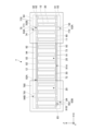
- FIG. 1 is a cross-sectional view showing a capacitor according to a first embodiment.
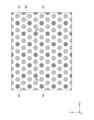
- FIG. 2 is a plan view showing the arrangement of internal electrodes in the capacitor according to the first embodiment.
- FIG. 3 is a flowchart showing a method for manufacturing a capacitor according to the first embodiment.
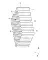
- FIG. 4 is a perspective view (part 1) showing the method for manufacturing the capacitor according to the first embodiment.
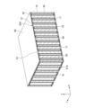
- FIG. 5 is a perspective view (part 2) showing the method for manufacturing the capacitor according to the first embodiment.
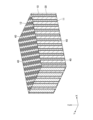
- FIG. 6 is a perspective view (part 3) showing the method for manufacturing the capacitor according to the first embodiment.
- FIG. 7 is a perspective view (part 4) showing the method for manufacturing the capacitor according to the first embodiment.
- FIG. 8 is a cross-sectional view showing a capacitor according to the second embodiment.
- FIG. 9 is a plan view showing the arrangement of internal electrodes in a capacitor according to the second embodiment.
- FIG. 10 is a perspective view (part 1) showing a method for manufacturing a capacitor according to the second embodiment.
- FIG. 11 is a perspective view (part 2) showing the method for manufacturing a capacitor according to the second embodiment.
- FIG. 12 is a perspective view (part 3) showing the method for manufacturing the capacitor according to the second embodiment.
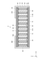
- FIG. 13 is a cross-sectional view showing a capacitor according to the third embodiment.
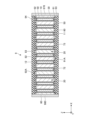
- FIG. 14 is a cross-sectional view showing a capacitor according to the fourth embodiment.
- FIG. 15 is a cross-sectional view showing a capacitor according to a fifth embodiment.
- FIG. 16 is a cross-sectional view showing a capacitor in accordance with a sixth embodiment.
- FIG. 10 is a perspective view (part 1) showing a method for manufacturing a capacitor according to the second embodiment.
- FIG. 11 is a perspective view (part 2) showing the method for manufacturing a capacitor according to
- FIG. 17 is a front view showing a capacitor according to the seventh embodiment.
- FIG. 18 is a cross-sectional view showing a capacitor according to an eighth embodiment.
- FIG. 19 is a cross-sectional view showing a capacitor according to a ninth embodiment.
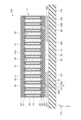
- FIG. 20 is a cross-sectional view showing a mounting board according to the tenth embodiment.
- Fig. 1 is a cross-sectional view showing a capacitor according to the first embodiment.
- Fig. 2 is a plan view showing the arrangement of internal electrodes in the capacitor according to the first embodiment.
- Fig. 1 corresponds to a cross-sectional view taken along line II in Fig. 2.
- the capacitor 1 has a substrate 10, a plurality of through holes 20, a dielectric film 30, a plurality of internal electrodes 50, a plurality of internal electrodes 60, an external electrode 70, an external electrode 80, an insulating layer 91, and an insulating layer 92. Note that the external electrode 80 and the insulating layer 92 are omitted in Figure 2.
- the substrate 10 is conductive.
- the substrate 10 includes, for example, silicon (Si), hafnium (Hf), lanthanum (La), niobium (Nb), tantalum (Ta), titanium (Ti), or zirconium (Zr).
- the substrate 10 may be composed of Si, Hf, La, Nb, Ta, Ti, or Zr. When Si is used as the material of the substrate 10, the substrate 10 is doped with impurities.
- the substrate 10 has a main surface 11 and a main surface 12 opposite to the main surface 11. In one example, the main surface 11 and the main surface 12 are perpendicular to the Z-axis direction, the main surface 11 is the lower surface, and the main surface 12 is the upper surface.
- the main surface 11 is an example of a first main surface
- the main surface 12 is an example of a second main surface.
- the shape of the substrate 10 is, for example, approximately rectangular.
- the dimension of the substrate 10 in the X-axis direction is 100 ⁇ m to 5000 ⁇ m
- the dimension in the Y-axis direction is 50 ⁇ m to 3000 ⁇ m
- the dimension in the Z-axis direction is 10 ⁇ m to 3000 ⁇ m.
- the plurality of through holes 20 are formed in the substrate 10.
- the through holes 20 penetrate the substrate 10 from the main surface 11 to the main surface 12.
- the cross-sectional shape of the through holes 20 perpendicular to the longitudinal direction is, for example, a circle with a diameter of 0.01 ⁇ m to 20 ⁇ m.
- the plurality of through holes 20 are arranged in a triangular lattice shape in a planar view.
- the plurality of through holes 20 are arranged in a regular triangular lattice shape with one side of the smallest unit triangle aligned in the X-axis direction.
- the pitch of the through holes 20 is, for example, 0.02 ⁇ m to 50 ⁇ m.
- the cross-sectional shape of the through holes 20 perpendicular to the longitudinal direction does not have to be circular, and may be, for example, rectangular or elliptical, but a circular shape is preferable from the viewpoint of ease of processing.
- the plurality of through holes 20 can be arranged in various ways in a planar view, but when they are arranged in a triangular lattice shape, for example, it is preferable that the cross-sectional shape of the through holes 20 perpendicular to the longitudinal direction be hexagonal rather than circular, considering the opposing faces of each other.
- the shape of the cross section perpendicular to the longitudinal direction of the through holes 20 can be set appropriately depending on the arrangement of the multiple through holes 20 in a plan view and the ease of processing.
- the dielectric film 30 covers the surface of the substrate 10.
- the surface of the substrate 10 includes the inner wall surface of the through hole 20.
- the dielectric film 30 is, for example, an oxide film, a nitride film, or an oxynitride film containing the same elements as the substrate 10.
- the substrate 10 is a conductive Si substrate
- the dielectric film 30 is a Si oxide film, a nitride film, or an oxynitride film.
- the thickness of the dielectric film 30 is, for example, 1 nm to 1000 nm.
- the dielectric film 30 is homogeneous and has a uniform thickness, so that it can be a capacitor with little variation in capacitance and good voltage resistance characteristics.
- Each of the multiple internal electrodes 50 fills one through hole 20 inside the dielectric film 30.
- each of the multiple internal electrodes 60 fills another through hole 20 inside the dielectric film 30.
- two internal electrodes 50 and one internal electrode 60 are repeatedly arranged between the multiple through holes 20 arranged in a direction parallel to the side of the smallest unit triangle of the regular triangular lattice formed by the multiple through holes 20.
- the direction parallel to the side of the smallest unit triangle of the regular triangular lattice formed by the multiple through holes 20 is the X-axis direction and two directions inclined by 60° clockwise or counterclockwise from the X-axis direction in the XY plane.
- the internal electrodes 50 and 60 include, for example, nickel (Ni), copper (Cu), palladium (Pd), platinum (Pt), silver (Ag), gold (Au), ruthenium (Ru), tungsten (W), molybdenum (Mo), titanium (Ti), or conductive silicon.
- the internal electrodes 50 and 60 may include an alloy material containing one or more of these metal elements.
- the internal electrodes 50 and 60 may include other metal elements.
- the internal electrodes 50 and 60 are an example of a first internal electrode, and the internal electrodes 60 are an example of a second internal electrode.
- the arrangement of the multiple through holes 20 in a plan view is such that the first internal electrode and the second internal electrode have a large opposing area.
- the internal electrode 50, which is a part of the first internal electrode, and the internal electrode 60, which is a part of the second internal electrode may be arranged at two diagonal points of each unit lattice of a square lattice, a rectangular lattice, or a rhombic lattice.
- An asymmetric arrangement such as a parallelepiped lattice is also acceptable, but a symmetric arrangement is preferable in order to achieve uniform capacitor characteristics.
- the insulating layer 91 covers the main surface 11 of the substrate 10 from below, sandwiching the dielectric film 30 therebetween.
- the insulating layer 91 further covers the lower surfaces of the internal electrodes 50 and 60.
- the insulating layer 92 covers the main surface 12 of the substrate 10 from above, sandwiching the dielectric film 30 therebetween.
- the insulating layer 92 further covers the upper surfaces of the internal electrodes 50 and 60.
- the material of the insulating layer 91 and the insulating layer 92 is, for example, a resin material such as polyimide, or an inorganic material such as silicon oxide (SiO 2 ), silicon nitride (SiN), or silicon oxynitride (SiON).
- the material of the insulating layer 91 and the insulating layer 92 may be an insulating material other than these.
- the insulating layer 91 and the insulating layer 92 can protect the substrate 10, the dielectric film 30, the internal electrodes 50, and the internal electrodes 60 from the external environment.
- the thickness of the insulating layer 91 and the insulating layer 92 is, for example, 10 nm to 5000 nm.
- a plurality of contact holes 91A are formed in the insulating layer 91, penetrating the insulating layer 91 in the Z-axis direction and reaching the underside of the internal electrode 50. At least a portion of the underside of the internal electrode 50 is exposed from each of the contact holes 91A.
- a plurality of contact holes 92A are formed in the insulating layer 92, penetrating the insulating layer 92 in the Z-axis direction and reaching the upper surface of the internal electrode 60. At least a portion of the upper surface of the internal electrode 60 is exposed from each of the contact holes 92A.
- the external electrode 70 is provided so as to contact the lower surface of the insulating layer 91.
- the external electrode 70 has a plurality of lead-out portions 71 each located in the contact hole 91A.
- the upper end of the lead-out portion 71 contacts the internal electrode 50, and the external electrode 70 is electrically connected to the plurality of internal electrodes 50.
- the external electrode 80 is provided so as to contact the upper surface of the insulating layer 92.
- the external electrode 80 has a plurality of lead-out portions 81 each located in the contact hole 92A. The lower end of the lead-out portion 81 contacts the internal electrode 60, and the external electrode 80 is electrically connected to the plurality of internal electrodes 60.
- the external electrode 70 and the external electrode 80 include, for example, copper (Cu), nickel (Ni), tin (Sn), palladium (Pd), platinum (Pt), silver (Ag), or gold (Au).
- the external electrode 70 and the external electrode 80 may include an alloy material including one or more of these metal elements.
- the external electrode 70 and the external electrode 80 may include other metal elements.
- the thickness of the external electrode 70 and the external electrode 80 is, for example, 100 nm to 10,000 nm.
- the lead-out portion 71 and the lead-out portion 81 may be formed independently of the external electrode 70 and the external electrode 80, respectively.
- the lead-out portion 71 and the lead-out portion 81 may be a part of the internal electrode 50 and the internal electrode 60, respectively, and may be made of the same material as the internal electrode 50 and the internal electrode 60, respectively.
- the lead-out portion 71 and the lead-out portion 81 are conductor portions independent of the internal electrode 50 and the external electrode 70, and the internal electrode 60 and the external electrode 80, respectively, and may be made of a different material from each of them, but if the thermal shrinkage rate of the material is taken into consideration, it is preferable that the lead-out portion 71 and the lead-out portion 81 are made of the same material as either or both of the materials.
- the internal electrode 50 functions as a first internal electrode of a first polarity
- the internal electrode 60 functions as a second internal electrode of a second polarity.
- the external electrode 70 is an example of a first external electrode
- the external electrode 80 is an example of a second external electrode.
- FIG. 3 is a flowchart showing the method for manufacturing the capacitor according to the first embodiment.
- FIG. 4 to FIG. 7 are perspective views showing the method for manufacturing the capacitor according to the first embodiment.
- a substrate 10 having a main surface 11 and a main surface 12 is prepared, and a plurality of through holes 20 are formed in the substrate 10 (step S1).
- a resist mask having openings exposing the areas where the through holes 20 are to be formed is formed on the main surface 11 or the main surface 12 by photolithography, and deep reactive ion etching (RIE) is performed using this resist mask.
- the deep RIE can be performed by, for example, the Bosch method.
- a wet etching process such as a photoassisted electrolytic etching method may be used. When the wet etching process is used, costs can be reduced compared to the Bosch method.
- the Bosch method uses greenhouse gases, but the wet etching process does not require greenhouse gases, so the burden on the global environment can be reduced.
- a dielectric film 30 is formed on the surface of the substrate 10, including the inner wall surface of the through hole 20 (step S2).
- the dielectric film 30 is formed, for example, by thermally oxidizing the substrate 10.
- an oxide film containing the same elements as the substrate 10 is formed as the dielectric film 30.
- thermal nitridation or thermal oxynitridation of the substrate 10 may be performed.
- thermal nitridation of the substrate 10 a nitride film containing the same elements as the substrate 10 is formed as the dielectric film 30, and by thermal oxynitridation of the substrate 10, an oxynitride film containing the same elements as the substrate 10 is formed as the dielectric film 30.
- the internal electrodes 50 and 60 that fill the through hole 20 on the inside of the dielectric film 30 are formed (step S3).
- the internal electrodes 50 and 60 can be formed, for example, by a plating method.
- the internal electrodes 50 and 60 may be formed by filling and firing a conductive paste.
- an insulating layer 91 is formed to cover the main surface 11 of the substrate 10 from below with the dielectric film 30 sandwiched therebetween, and an insulating layer 92 is formed to cover the main surface 12 of the substrate 10 from above with the dielectric film 30 sandwiched therebetween (step S4).
- a plurality of contact holes 91A are formed in the insulating layer 91, and a plurality of contact holes 92A are formed in the insulating layer 92.
- the insulating layers 91 and 92 can be formed, for example, by chemical vapor deposition (CVD) method.
- the contact holes 91A and 92A can be formed, for example, by etching using a mask.
- an external electrode 70 having an extension 71 is formed so as to contact the lower surface of the insulating layer 91, and an external electrode 80 having an extension 81 is formed so as to contact the upper surface of the insulating layer 92 (step S5).
- the external electrodes 70 and 80 can be formed, for example, by a sputtering method.
- the capacitor 1 according to the first embodiment can be manufactured.
- the external electrode 70 may be formed after the insulating layer 91 is formed, and the insulating layer 92 and the external electrode 80 may be formed in this order after the external electrode 70 is formed.
- the external electrode 80 may be formed after the insulating layer 92 is formed, and the insulating layer 91 and the external electrode 70 may be formed in this order after the external electrode 80 is formed.
- a plurality of through holes 20 penetrate the substrate 10, and a dielectric film 30 covers the surface of the substrate 10, including the inner wall surfaces of the plurality of through holes 20.
- a dielectric film 30 can be formed by thermal oxidation, thermal nitridation, or thermal oxynitridation of the substrate 10.
- the through holes 20 the area in which the substrate 10 and the internal electrode 50 or the internal electrode 60 face each other becomes larger than when a bottomed hole is formed instead of the through holes 20. For this reason, a large capacity can be obtained.
- a thin dielectric film 30 can be formed with a stable thickness by thermal oxidation, thermal nitridation, or thermal oxynitridation.
- the oxidizing gas or nitriding gas used to form the dielectric film 30 can be uniformly supplied into the through holes 20.
- the through holes 20 can be easily filled with a conductive material without forming voids (voids). Therefore, the capacitor 1 can easily and stably obtain a large capacity.
- the dielectric film 30, the conductive substrate 10, and the dielectric film 30 are sandwiched in this order between the adjacent internal electrodes 50 of the first polarity and the internal electrodes 60 of the second polarity. This ensures a high degree of symmetry between the internal electrodes 50 of the first polarity and the internal electrodes 60 of the second polarity. Therefore, when the material of the internal electrodes 50 and the material of the internal electrodes 60 are the same, the effect of polarity on the characteristics of the capacitor 1 can be suppressed.
- the dielectric film 30 is a silicon nitride film
- the barrier properties of the substrate 10 can be improved compared to when the dielectric film 30 is a silicon oxide film.
- the dielectric film 30 is formed by thermal oxidation, thermal nitridation, or thermal oxynitridation of the substrate 10, it is easier to reduce manufacturing costs and time than when the dielectric film 30 is formed by atomic layer deposition (ALD) or CVD.
- ALD atomic layer deposition
- the equivalent series inductance (ESL) and equivalent series resistance (ESR) can be reduced compared to when they are arranged inside a bottomed hole.
- Fig. 8 is a cross-sectional view showing a capacitor according to the second embodiment.
- Fig. 9 is a plan view showing the arrangement of the internal electrodes in the capacitor according to the second embodiment.
- Fig. 8 corresponds to a cross-sectional view taken along line VIII-VIII in Fig. 9.
- the capacitor 2 has a substrate 10, a plurality of through holes 20, a dielectric film 30, a plurality of internal electrodes 40, an external electrode 70, an external electrode 80, and a plurality of insulating layers 95. Note that the external electrode 70 and the insulating layer 95 are omitted in Figure 9.
- the configuration of the substrate 10 and the through hole 20 is the same as in the first embodiment.
- the configuration of the dielectric film 30 is the same as in the first embodiment, except that it is not formed on the main surface 12 of the substrate 10.
- Each of the multiple internal electrodes 40 fills one through hole 20 inside the dielectric film 30.
- the internal electrodes 40 are made of, for example, the same material as the internal electrodes 50 and 60.
- Each of the multiple insulating layers 95 covers the upper surface of the internal electrode 40.
- the insulating layers 95 are made of, for example, the same material as the insulating layers 91 and 92.
- the thickness of the insulating layers 95 is, for example, 10 nm to 5000 nm.
- the external electrode 70 is provided so as to contact the main surface 12 of the substrate 10 and the upper surfaces of the multiple insulating layers 95.
- the external electrode 70 is electrically connected to the substrate 10.
- the external electrode 80 is provided so as to contact the lower surfaces of the multiple internal electrodes 40 and the lower surface of the dielectric film 30.
- the external electrode 80 is electrically connected to the internal electrode 40.
- voltages of different polarities are applied between the external electrode 70 and the external electrode 80.
- the conductive substrate 10 functions as an internal electrode of a first polarity
- the internal electrode 40 functions as an internal electrode of a second polarity.
- Figures 10 to 12 are perspective views showing the method for manufacturing the capacitor according to the second embodiment.
- the substrate 10 is prepared, and a plurality of through holes 20 are formed in the substrate 10 (see FIG. 4).
- a dielectric film 30 is formed on the surface of the substrate 10, including the inner wall surfaces of the through holes 20.
- an internal electrode 40 is formed to fill the through holes 20 inside the dielectric film 30.
- the internal electrode 40 can be formed by, for example, a plating method.
- the internal electrode 40 may also be formed by filling and firing a conductive paste.
- the portion of the dielectric film 30 covering the main surface 12 of the substrate 10 is removed by etching. As a result, the main surface 12 of the substrate 10 is exposed.
- a plurality of insulating layers 95 are formed to cover the upper surface of the internal electrode 40.
- the plurality of insulating layers 95 can be formed, for example, by forming and processing the main surface 12 of the insulating layer that will become the plurality of insulating layers 95 and the upper surface of the internal electrode 40 as a whole.
- an external electrode 70 is formed so as to contact the main surface 12 of the substrate 10 and the upper surface of the insulating layer 95, and an external electrode 80 is formed so as to contact the lower surfaces of the multiple internal electrodes 40 and the lower surface of the dielectric film 30.
- the capacitor 2 according to the second embodiment can be manufactured.
- the capacitor 2 according to the second embodiment can easily and stably obtain a large capacity, just like the first embodiment.
- a third embodiment differs from the first embodiment mainly in the configuration of the external electrodes.
- Fig. 13 is a cross-sectional view showing a capacitor according to the third embodiment.
- the capacitor 3 has, in addition to the configuration of the capacitor 1, a collector electrode 72, a collector electrode 82, an insulating layer 93, an insulating layer 94, and a connection portion 74.
- the capacitor 3 has an external electrode 370 and an external electrode 380 instead of the external electrode 70 and the external electrode 80.
- the configurations of the substrate 10, through hole 20, dielectric film 30, internal electrode 50, internal electrode 60, and insulating layer 91 are the same as those in the first embodiment.
- the configuration of the insulating layer 92 is the same as that in the first embodiment, except that in addition to the multiple contact holes 92A, a contact hole 92B is formed.
- the contact hole 92B penetrates the insulating layer 92 in the Z-axis direction and reaches the top surface of one of the internal electrodes 50. At least a portion of the top surface of the internal electrode 50 is exposed from the contact hole 92B.
- the collector electrode 72 is provided so as to contact the lower surface of the insulating layer 91.
- the collector electrode 72 has a plurality of lead-out portions 73 each located in the contact hole 91A.
- the upper end of the lead-out portion 73 contacts the internal electrode 50, and the collector electrode 72 is electrically connected to the internal electrode 50.
- the collector electrode 82 is provided so as to contact the upper surface of the insulating layer 92.
- the collector electrode 82 has a plurality of lead-out portions 83 each located in the contact hole 92A. The lower end of the lead-out portion 83 contacts the internal electrode 60, and the collector electrode 82 is electrically connected to the internal electrode 60.
- connection portion 74 is provided away from the collector electrode 82 so as to contact the upper surface of the insulating layer 92.
- the connection portion 74 has a lead-out portion 75 located in the contact hole 92B. The lower end of the lead-out portion 75 contacts the internal electrode 50, and the connection portion 74 is electrically connected to the internal electrode 50.
- the collector electrodes 72, 82, and connection parts 74 are made of, for example, the same material as the external electrodes 70 and 80.
- the thicknesses of the collector electrodes 72, 82, and connection parts 74 are, for example, 10 nm to 5000 nm.
- Insulating layer 93 covers the lower surface of insulating layer 91 from below, sandwiching collector electrode 72 therebetween.
- Insulating layer 94 covers the upper surface of insulating layer 92 from above, sandwiching collector electrode 82 and connection portion 74 therebetween.
- Insulating layers 93 and 94 are made of, for example, the same material as insulating layers 91 and 92.
- the thickness of insulating layers 93 and 94 is, for example, 10 nm to 5000 nm.
- Insulating layer 94 is formed with contact hole 94A, which penetrates insulating layer 94 in the Z-axis direction and reaches the top surface of connection portion 74, and contact hole 94B, which penetrates insulating layer 94 in the Z-axis direction and reaches the top surface of collector electrode 82. At least a portion of the top surface of connection portion 74 is exposed from contact hole 94A, and at least a portion of the top surface of collector electrode 82 is exposed from contact hole 94B.
- the external electrode 370 is provided so as to contact the upper surface of the insulating layer 94.
- the external electrode 370 has a lead portion 371 located in the contact hole 94A. The lower end of the lead portion 371 is in contact with the connection portion 74, and the external electrode 370 is electrically connected to the internal electrode 50 via the connection portion 74.
- the multiple internal electrodes 50 are electrically connected to the collecting electrode 72. Therefore, the external electrode 370 is electrically connected to the multiple internal electrodes 50.
- the external electrode 380 is provided so as to contact the upper surface of the insulating layer 94.
- the external electrode 380 has a lead portion 381 located in the contact hole 94B.
- the lower end of the lead portion 381 is in contact with the collecting electrode 82, and the external electrode 380 is electrically connected to the multiple internal electrodes 60 via the collecting electrode 82.
- the external electrode 370 and the external electrode 380 are, for example, made of the same material as the external electrode 70 and the external electrode 80.
- the third embodiment can achieve the same effects as the first embodiment.
- the capacitor 3 according to the third embodiment is mounted on a circuit board, for example, with the main surface 12 facing the circuit board.
- a fourth embodiment differs from the third embodiment mainly in the configuration of the external electrodes.
- Fig. 14 is a cross-sectional view showing a capacitor according to the fourth embodiment.
- the capacitor 4 according to the fourth embodiment has an external electrode 470 and an external electrode 480 instead of the external electrode 370 and the external electrode 380.
- the external electrode 470 is in contact with the upper surface of the insulating layer 94 and is provided so as to cover the +X side surface of the substrate 10 from above the dielectric film 30.
- the external electrode 470 has a lead portion 471 located in the contact hole 94A. The lower end of the lead portion 471 is in contact with the connection portion 74, and the external electrode 470 is electrically connected to the internal electrode 50.
- the external electrode 480 is in contact with the upper surface of the insulating layer 94 and is provided so as to cover the -X side surface of the substrate 10 from above the dielectric film 30.
- the external electrode 480 has a lead portion 481 located in the contact hole 94B. The lower end of the lead portion 481 is in contact with the collecting electrode 82, and the external electrode 480 is electrically connected to the internal electrode 60.
- the external electrodes 470 and 480 are made of, for example, the same material as the external electrodes 70 and 80.
- the fourth embodiment can also provide the same effects as those of the third embodiment. Furthermore, in the fourth embodiment, when a fluid conductive adhesive is used for mounting to a circuit board, the conductive adhesive can be made to wet and spread over a wide area of the external electrodes 470 and 480, resulting in higher mounting reliability.
- a fifth embodiment differs from the fourth embodiment mainly in the configuration of the external electrodes.
- Fig. 15 is a cross-sectional view showing a capacitor according to the fifth embodiment.
- the capacitor 5 according to the fifth embodiment has an external electrode 570 and an external electrode 580 instead of the external electrode 470 and the external electrode 480.
- the capacitor 5 has a connection portion 84 in addition to the configuration of the capacitor 4.
- a contact hole 91B is formed in the insulating layer 91.
- the contact hole 91B penetrates the insulating layer 91 in the Z-axis direction and reaches the lower surface of one internal electrode 60. At least a part of the lower surface of the internal electrode 60 is exposed from the contact hole 91B.
- the connection portion 84 is provided away from the collecting electrode 72 so as to contact the lower surface of the insulating layer 91.
- the connection portion 84 has a lead portion 85 located in the contact hole 91B. The upper end of the lead portion 85 contacts the internal electrode 60, and the connection portion 84 is electrically connected to the internal electrode 60.
- Insulating layer 93 is formed with contact hole 93A, which penetrates insulating layer 93 in the Z-axis direction and reaches the underside of collector electrode 72, and contact hole 93B, which penetrates insulating layer 93 in the Z-axis direction and reaches the underside of connection portion 84. At least a portion of the underside of collector electrode 72 is exposed from contact hole 93A, and at least a portion of the underside of connection portion 84 is exposed from contact hole 93B.
- the external electrode 570 has a portion in contact with the lower surface of the insulating layer 93 and a lead portion 576 located in the contact hole 93A in addition to the configuration of the external electrode 470.
- the upper end of the lead portion 576 is in contact with the collector electrode 72, and the external electrode 570 is electrically connected to the internal electrode 50 via the collector electrode 72 in addition to the connection portion 74.
- the external electrode 580 has a portion in contact with the lower surface of the insulating layer 93 and a lead portion 586 located in the contact hole 93B in addition to the configuration of the external electrode 480.
- the upper end of the lead portion 586 is in contact with the connection portion 84, and the external electrode 580 is electrically connected to the internal electrode 60 via the connection portion 84 in addition to the collector electrode 82.
- the external electrode 570 and the external electrode 580 are made of, for example, the same material as the external electrode 70 and the external electrode 80.
- the capacitor 3 according to the fifth embodiment can be mounted on a circuit board, for example, with either the main surface 11 or the main surface 12 facing the circuit board.
- a sixth embodiment differs from the fifth embodiment mainly in the configuration of the external electrodes.
- Fig. 16 is a cross-sectional view showing a capacitor according to the sixth embodiment.
- the capacitor 6 according to the sixth embodiment has an external electrode 370 and an external electrode 670 instead of the external electrode 570, and an external electrode 380 and an external electrode 680 instead of the external electrode 580.
- the external electrode 670 is provided so as to contact the lower surface of the insulating layer 93, and has a lead portion 676 located in the contact hole 93A. The upper end of the lead portion 676 contacts the collector electrode 72, and the external electrode 670 is electrically connected to the internal electrode 50 via the collector electrode 72.
- the external electrode 680 is provided so as to contact the lower surface of the insulating layer 93, and has a lead portion 686 located in the contact hole 93B.
- the upper end of the lead portion 686 contacts the connection portion 84, and the external electrode 680 is electrically connected to the internal electrode 60 via the connection portion 84.
- the external electrode 670 and the external electrode 680 are made of, for example, the same material as the external electrode 70 and the external electrode 80.
- a seventh embodiment differs from the fifth embodiment mainly in the configuration of the external electrodes.
- Fig. 17 is a front view showing the capacitor according to the seventh embodiment.
- the capacitor 7 according to the seventh embodiment has an external electrode 770 and an external electrode 780 instead of the external electrode 570 and the external electrode 580.
- the external electrode 770 has a lead portion 771 located in the contact hole 94A and a lead portion 772 located in the contact hole 93A. The lower end of the lead portion 771 contacts the connection portion 74, and the upper end of the lead portion 772 contacts the collector electrode 72, and the external electrode 770 is electrically connected to the internal electrode 50.
- the external electrode 780 has a lead portion 781 located in the contact hole 94B and a lead portion 782 located in the contact hole 93B. The lower end of the lead portion 781 contacts the collector electrode 82, and the upper end of the lead portion 782 contacts the connection portion 84, and the external electrode 780 is electrically connected to the internal electrode 60.
- external electrode 770 and external electrode 780 have portions covering two side surfaces perpendicular to the Y-axis direction. That is, external electrode 770 covers five surfaces of substrate 10: the +Z side surface (principal surface 12), the -Z side surface (principal surface 11), the +X side surface, the +Y side surface, and the -Y side surface. External electrode 780 covers five surfaces of substrate 10: the +Z side surface (principal surface 12), the -Z side surface (principal surface 11), the -X side surface, the +Y side surface, and the -Y side surface.
- the +Y side surface and the -Y side surface of substrate 10 are covered by dielectric film 30, and external electrode 770 and external electrode 780 cover the +Y side surface and the -Y side surface of substrate 10 from above dielectric film 30.
- the +Y side surface and the -Y side surface of the substrate 10 may be covered with a dielectric film 30 and an insulating layer made of the same material as the insulating layers 91 and 92.
- the external electrodes 770 and 780 are made of, for example, the same material as the external electrodes 70 and 80.
- the seventh embodiment can also provide the same effects as those of the fifth embodiment. Furthermore, in the seventh embodiment, when a fluid conductive adhesive is used for mounting to a circuit board, the conductive adhesive can be made to wet and spread over a wide area of the external electrodes 770 and 780, resulting in higher mounting reliability.
- Fig. 18 is a cross-sectional view showing a capacitor according to the eighth embodiment.
- the capacitor 8 according to the eighth embodiment has, in addition to the configuration of the capacitor 1, a collector electrode 72, a collector electrode 82, an insulating layer 93, and an insulating layer 94, as in the third embodiment. Furthermore, the capacitor 8 according to the eighth embodiment has an external electrode 870 and an external electrode 880 instead of the external electrode 70 and the external electrode 80.
- the multiple internal electrodes 50 and the collector electrode 72 are exposed from the side surface of the +X side of the substrate 10, and the multiple internal electrodes 60 and the collector electrode 82 are exposed from the side surface of the -X side of the substrate 10.
- the external electrode 870 is in contact with the multiple internal electrodes 50 and the collector electrode 72 exposed from the side surface of the +X side of the substrate 10.
- the external electrode 880 is in contact with the multiple internal electrodes 60 and the collector electrode 82 exposed from the side surface of the -X side of the substrate 10. Therefore, the external electrode 870 is electrically connected to the multiple internal electrodes 50 via the collector electrode 72, and the external electrode 880 is electrically connected to the multiple internal electrodes 60 via the collector electrode 82.
- the external electrode 870 and the external electrode 880 have a portion that is in contact with the upper surface of the insulating layer 94.
- the external electrode 870 and the external electrode 880 are made of, for example, the same material as the external electrode 70 and the external electrode 80.
- the capacitor 8 according to the eighth embodiment is mounted on a circuit board, for example, with the main surface 12 facing the circuit board. Furthermore, when a fluid conductive adhesive is used for mounting on the circuit board, the conductive adhesive can be made to wet and spread over a wide area of the external electrodes 870 and 880, resulting in higher mounting reliability.
- a ninth embodiment will be described.
- the ninth embodiment differs from the eighth embodiment mainly in the configuration of the external electrodes.
- Fig. 19 is a cross-sectional view showing a capacitor according to the ninth embodiment.
- the capacitor 9 according to the ninth embodiment has external electrodes 970 and 980 instead of external electrodes 870 and 880.
- the external electrodes 970 and 980 do not have any portions that contact the upper surface of the insulating layer 94.
- the tenth embodiment relates to a mounting board having a capacitor.
- Fig. 20 is a cross-sectional view showing the mounting board according to the tenth embodiment.
- the mounting board 100 has a circuit board 110 and the capacitor 3 according to the third embodiment.
- the circuit board 110 is provided with a connection land 101 and a connection land 102.
- the capacitor 3 is mounted on the circuit board 110.
- An external electrode 370 is joined to the connection land 101, and an external electrode 380 is joined to the connection land 102.
- the mounting board 100 can be mounted on various electronic devices. Examples of electronic devices equipped with the mounting board 100 include smartphones, mobile phones, tablet terminals, and game consoles.
- capacitors 1, 2, 4, 5, 6, 7, 8, or 9 may be used instead of capacitor 3.
- the shape of the cross section perpendicular to the longitudinal direction of the through hole 20 is not limited to a circle, and may be other shapes such as a square, rectangular, triangular, hexagonal, or zigzag shape.
- the multiple through holes 20 may be arranged in other layouts such as a square lattice.
- the arrangement of the multiple internal electrodes 50 and the multiple internal electrodes 60 arranged in the closest packing direction in a plan view perpendicular to the main surface 12 is not limited to the above example, and for example, one internal electrode 50 and one internal electrode 60 may be arranged repeatedly.
- the through hole 20 may have a tapered inner wall surface whose opening area narrows as it moves away from the main surface 11, or may have a tapered inner wall surface whose opening area narrows as it moves away from the main surface 12.
- a conductive substrate having a first main surface and a second main surface opposite to the first main surface; A plurality of through holes formed in the base material and penetrating from the first main surface to the second main surface; a dielectric film covering a surface of the base material including inner wall surfaces of the plurality of through holes; a plurality of internal electrodes filling the plurality of through holes on the inside of the dielectric film; A capacitor having
- the plurality of internal electrodes are a plurality of first internal electrodes of a first polarity; a plurality of second internal electrodes of a second polarity different from the first polarity;
- ⁇ 3> a first external electrode electrically connected to the plurality of first internal electrodes; a second external electrode electrically connected to the plurality of second internal electrodes;
- ⁇ 4> The capacitor described in ⁇ 2> or ⁇ 3>, wherein two of the first internal electrodes and one of the second internal electrodes are repeatedly arranged between the plurality of first internal electrodes and the plurality of second internal electrodes arranged in a close-packed direction in a planar view perpendicular to the second main surface.
- ⁇ 6> The capacitor according to any one of ⁇ 1> to ⁇ 5>, wherein the dielectric film is an oxide film, a nitride film, or an oxynitride film containing the same element as the substrate.
- ⁇ 7> The capacitor according to any one of ⁇ 1> to ⁇ 6>, wherein the substrate contains silicon, hafnium, lanthanum, niobium, tantalum, titanium, or zirconium.
- ⁇ 8> A circuit board; The capacitor according to any one of ⁇ 1> to ⁇ 7>, which is mounted on the circuit board; A mounting board having the same.
- the method for manufacturing a capacitor comprising the steps of:
- ⁇ 10> The method for manufacturing a capacitor according to ⁇ 9>, wherein the plurality of internal electrodes are formed as a plurality of first internal electrodes of a first polarity and a plurality of second internal electrodes of a second polarity different from the first polarity.
- ⁇ 11> forming a first external electrode electrically connected to the plurality of first internal electrodes; forming a second external electrode electrically connected to the plurality of second internal electrodes; The method for producing a capacitor according to ⁇ 10>,
- ⁇ 12> forming a first external electrode electrically connected to the base material; forming a second external electrode electrically connected to the plurality of internal electrodes; The method for producing a capacitor according to ⁇ 9>,
- Capacitor 10 Substrate 11, 12: Main surface 20: Through hole 30: Dielectric film 40, 50, 60: Internal electrode 70, 80, 370, 380, 470, 480, 570, 580, 670, 680, 770, 780, 870, 880, 970, 980 External electrode 100: Mounting board 101, 102: Connection land 110: Circuit board
Landscapes
- Engineering & Computer Science (AREA)
- Power Engineering (AREA)
- Microelectronics & Electronic Packaging (AREA)
- Manufacturing & Machinery (AREA)
- Chemical & Material Sciences (AREA)
- Inorganic Chemistry (AREA)
- Fixed Capacitors And Capacitor Manufacturing Machines (AREA)
Abstract
コンデンサは、第1主面と、前記第1主面とは反対側の第2主面とを有する導電性の基材と、前記基材に形成され、前記第1主面から前記第2主面まで貫通する複数の貫通孔と、前記複数の貫通孔の内壁面を含む、前記基材の表面を覆う誘電体膜と、前記誘電体膜の内側で前記複数の貫通孔を各々充填する複数の内部電極と、を有する。
Description
本開示は、コンデンサ、実装基板及びコンデンサの製造方法に関する。
導電性を有するシリコン基板に複数の有底のトレンチを形成し、トレンチの底面及び側面に複数の誘電体膜を形成し、誘電体膜の内側でトレンチを充填する電極を形成したコンデンサが提案されている。
従来のコンデンサにおいては、大きな容量を安定して得ることは容易でない。
本開示は、大きな容量を安定して得ることができるコンデンサ、実装基板及びコンデンサの製造方法を提供することを目的とする。
本開示の一態様によれば、コンデンサは、第1主面と、前記第1主面とは反対側の第2主面とを有する導電性の基材と、前記基材に形成され、前記第1主面から前記第2主面まで貫通する複数の貫通孔と、前記複数の貫通孔の内壁面を含む、前記基材の表面を覆う誘電体膜と、前記誘電体膜の内側で前記複数の貫通孔を各々充填する複数の内部電極と、を有する。
本開示によれば、大きな容量を安定して得ることができる。
以下、本開示の実施形態について詳細に説明するが、本開示はこれらに限定されるものではない。なお、本明細書および図面において、実質的に同一の機能構成を有する構成要素については、同一の符号を付することにより重複した説明を省くことがある。また、以下の説明では、XYZ直交座標系を用いるが、当該座標系は、説明のために定めるものであって、コンデンサ及び実装基板の姿勢について限定するものではない。また、任意の点からみて、+Z側を上方、上側又は上ということがあり、-Z側を下方、下側又は下ということがある。本開示において、「平面視」とは、対象物を上方から見ることをいい、「平面形状」とは、対象物を上方から見た形状のことをいう。
(第1実施形態)
まず、第1実施形態について説明する。第1実施形態はコンデンサに関する。図1は、第1実施形態に係るコンデンサを示す断面図である。図2は、第1実施形態に係るコンデンサにおける内部電極の配置を示す平面図である。図1は、図2中のI-I線に沿った断面図に相当する。
まず、第1実施形態について説明する。第1実施形態はコンデンサに関する。図1は、第1実施形態に係るコンデンサを示す断面図である。図2は、第1実施形態に係るコンデンサにおける内部電極の配置を示す平面図である。図1は、図2中のI-I線に沿った断面図に相当する。
図1及び図2に示すように、第1実施形態に係るコンデンサ1は、基材10と、複数の貫通孔20と、誘電体膜30と、複数の内部電極50と、複数の内部電極60と、外部電極70と、外部電極80と、絶縁層91と、絶縁層92とを有する。なお、図2では、外部電極80及び絶縁層92を省略している。
基材10は導電性を有する。基材10は、例えば、シリコン(Si)、ハフニウム(Hf)、ランタン(La)、ニオブ(Nb)、タンタル(Ta)、チタン(Ti)又はジルコニウム(Zr)を含む。基材10が、Si、Hf、La、Nb、Ta、Ti又はZrから構成されてもよい。基材10の材料としてSiが用いられる場合、基材10には不純物がドーピングされる。基材10は、主面11と、主面11とは反対側の主面12とを有する。一例では、主面11及び主面12はZ軸方向に垂直であり、主面11が下面であり、主面12が上面である。主面11は第1主面の一例であり、主面12は第2主面の一例である。基材10の形状は、例えば略直方体状である。例えば、基材10のX軸方向の寸法は100μm~5000μmであり、Y軸方向の寸法は50μm~3000μmであり、Z軸方向の寸法は10μm~3000μmである。
複数の貫通孔20は基材10に形成されている。貫通孔20は基材10を主面11から主面12まで貫通する。貫通孔20の長手方向に垂直な断面の形状は、例えば直径が0.01μm~20μmの円形状である。本実施形態では、複数の貫通孔20は、平面視で三角格子状に配置されている。例えば、複数の貫通孔20は、最小単位の三角形の一辺がX軸方向に並ぶようにして正三角格子状に配置されている。貫通孔20のピッチは、例えば0.02μm~50μmである。貫通孔20の長手方向に垂直な断面の形状は円形状でなくてもよく、例えば矩形状や楕円状等であってもよいが、加工が容易である点からは円形状が望ましい。複数の貫通孔20は、平面視で様々な配置を取りうるが、例えば三角格子状に配置されている場合、貫通孔20の長手方向に垂直な断面の形状は円形状であるよりも、六角形の形状を取ることが、互いの面の対向を考えると望ましい。貫通孔20の長手方向に垂直な断面の形状は、複数の貫通孔20の平面視での配置の状況と加工の容易さにより適宜設定し得る。
誘電体膜30は基材10の表面を覆う。基材10の表面には貫通孔20の内壁面が含まれる。誘電体膜30は、例えば、基材10と同じ元素を含む酸化膜、窒化膜又は酸窒化膜である。例えば、基材10が導電性のSi基材であれば、誘電体膜30はSiの酸化膜、窒化膜又は酸窒化膜である。誘電体膜30の厚さは、例えば1nm~1000nmである。誘電体膜30は、均質かつ均厚であることで、静電容量のばらつきが少なく、耐圧特性が良好なコンデンサとすることができる。このため誘電体膜30を薄膜プロセスで基材10の表面に別途形成することは、貫通孔20の内壁面の主面に近い部分と遠い部分において均質かつ均厚とすることが困難であるため好ましくはない。
複数の内部電極50の各々は、誘電体膜30の内側で1つの貫通孔20を充填する。また、複数の内部電極60の各々は、誘電体膜30の内側で他の1つの貫通孔20を充填する。例えば、複数の貫通孔20が構成する正三角格子の最小単位の三角形の辺に平行な方向に並ぶ複数の貫通孔20の間では、2つの内部電極50と、1つの内部電極60とが繰り返し配置されている。本実施形態では、複数の貫通孔20が構成する正三角格子の最小単位の三角形の辺に平行な方向は、X軸方向、及び、XY面内でX軸方向から時計回り又は反時計回りに60°傾斜した2つの方向である。言い換えると、主面12に垂直な平面視で最密な方向に並ぶ複数の内部電極50及び複数の内部電極60の間では、2つの内部電極50と、1つの内部電極60とが繰り返し配置されている。内部電極50及び内部電極60は、例えば、ニッケル(Ni)、銅(Cu)、パラジウム(Pd)、白金(Pt)、銀(Ag)、金(Au)、ルテニウム(Ru)、タングステン(W)、モリブデン(Mo)、チタン(Ti)又は導電性シリコンを含む。内部電極50及び内部電極60がこれら金属元素の一又は複数を含む合金材料を含んでいてもよい。内部電極50及び内部電極60が他の金属元素を含んでいてもよい。内部電極50は第1内部電極の一例であり、内部電極60は第2内部電極の一例である。複数の貫通孔20の平面視での配置状況は、第1内部電極と第2内部電極が高い対向面積となるように配置される。例えば第1内部電極の一部である内部電極50と第2内部電極の一部である内部電極60とは正方格子、矩形格子、菱形格子のそれぞれの単位格子の2つの対角点にそれぞれ配置されることもできる。平行体格子のように非対称な配置であってもよいが、対称性を持った配置である方が均一なコンデンサの特性を実現する上で好ましい。
絶縁層91は、誘電体膜30を間に挟んで基材10の主面11を下方から覆う。絶縁層91は、更に、内部電極50及び内部電極60の下面を覆う。また、絶縁層92は、誘電体膜30を間に挟んで基材10の主面12を上方から覆う。絶縁層92は、更に、内部電極50及び内部電極60の上面を覆う。絶縁層91及び絶縁層92の材料は、例えば、ポリイミド等の樹脂材料、又は、酸化シリコン(SiO2)、窒化シリコン(SiN)、酸窒化シリコン(SiON)等の無機材料である。絶縁層91及び絶縁層92の材料がこれら以外の絶縁材料であってもよい。絶縁層91及び絶縁層92により、基材10、誘電体膜30、内部電極50及び内部電極60を外部環境から保護することができる。絶縁層91及び絶縁層92の厚さは、例えば10nm~5000nmである。
絶縁層91に、Z軸方向で絶縁層91を貫通し、内部電極50の下面に達する複数のコンタクトホール91Aが形成されている。コンタクトホール91Aの各々から内部電極50の下面の少なくとも一部が露出している。絶縁層92に、Z軸方向で絶縁層92を貫通し、内部電極60の上面に達する複数のコンタクトホール92Aが形成されている。コンタクトホール92Aの各々から内部電極60の上面の少なくとも一部が露出している。
外部電極70は、絶縁層91の下面に接するように設けられている。外部電極70は、各々がコンタクトホール91A内に位置する複数の引出部71を有する。引出部71の上端が内部電極50に接しており、外部電極70は複数の内部電極50に電気的に接続されている。外部電極80は、絶縁層92の上面に接するように設けられている。外部電極80は、各々がコンタクトホール92A内に位置する複数の引出部81を有する。引出部81の下端が内部電極60に接しており、外部電極80は複数の内部電極60に電気的に接続されている。外部電極70及び外部電極80は、例えば、銅(Cu)、ニッケル(Ni)、スズ(Sn)、パラジウム(Pd)、白金(Pt)、銀(Ag)又は金(Au)を含む。外部電極70及び外部電極80が、これら金属元素の一又は複数を含む合金材料を含んでいてもよい。外部電極70及び外部電極80が他の金属元素を含んでいてもよい。外部電極70及び外部電極80の厚さは、例えば100nm~10000nmである。引出部71及び引出部81はそれぞれ外部電極70及び外部電極80から独立して形成されていてもよい。引出部71及び引出部81はそれぞれ内部電極50及び内部電極60の一部となっていてもよく、それぞれ内部電極50及び内部電極60と同様の材料より構成されていてもよい。引出部71及び引出部81はそれぞれ内部電極50と外部電極70及び内部電極60と外部電極80から独立した導体部であって、それぞれと異なる材質より構成されることもできるが、材料の熱収縮率などを考慮するならば、どちらかもしくは双方の材質と共通の材質である方が好ましい。
外部電極70と外部電極80との間に極性が異なる電圧が印加される。この結果、内部電極50が第1極性の第1内部電極として機能し、内部電極60が第2極性の第2内部電極として機能する。外部電極70は第1外部電極の一例であり、外部電極80は第2外部電極の一例である。
次に、第1実施形態に係るコンデンサ1の製造方法について説明する。図3は、第1実施形態に係るコンデンサの製造方法を示すフローチャートである。図4~図7は、第1実施形態に係るコンデンサの製造方法を示す斜視図である。
まず、図4に示すように、主面11及び主面12を有する基材10を準備し、基材10に複数の貫通孔20を形成する(ステップS1)。貫通孔20の形成では、例えば、貫通孔20を形成する予定の領域を露出する開口部を備えたレジストマスクを主面11又は主面12にフォトリソグラフィ法により形成し、このレジストマスクを用いた深掘り反応性イオンエッチング(reactive ion etching:RIE)を行う。深掘りRIEは、例えばボッシュ法により行うことができる。ボッシュ法に代えて、光アシスト電解エッチング法などのウェットエッチングプロセスを用いてもよい。ウェットエッチングプロセスを用いた場合、ボッシュ法と比較して、コストを低減することができる。また、ボッシュ法では温室効果ガスが使用されるが、ウェットエッチングプロセスでは温室効果ガスを必要としないため、地球環境への負荷を低減できる。
次いで、図5に示すように、貫通孔20の内壁面を含め、基材10の表面に誘電体膜30を形成する(ステップS2)。誘電体膜30の形成では、例えば基材10の熱酸化を行う。基材10の熱酸化により、誘電体膜30として、基材10と同じ元素を含む酸化膜が形成される。誘電体膜30の形成の際に、基材10の熱窒化又は熱酸窒化を行ってもよい。基材10の熱窒化により、誘電体膜30として、基材10と同じ元素を含む窒化膜が形成され、基材10の熱酸窒化により、誘電体膜30として、基材10と同じ元素を含む酸窒化膜が形成される。次いで、誘電体膜30の内側で貫通孔20を充填する内部電極50及び内部電極60を形成する(ステップS3)。内部電極50及び内部電極60は、例えばめっき法により形成することができる。内部電極50及び内部電極60を導電性ペーストの充填及び焼成により形成してもよい。
次いで、図6に示すように、誘電体膜30を間に挟んで基材10の主面11を下方から覆う絶縁層91を形成し、誘電体膜30を間に挟んで基材10の主面12を上方から覆う絶縁層92を形成する(ステップS4)。次いで、絶縁層91に複数のコンタクトホール91Aを形成し、絶縁層92に複数のコンタクトホール92Aを形成する。絶縁層91及び絶縁層92は、例えば化学気相成長(chemical vapor deposition:CVD)法により形成することができる。コンタクトホール91A及びコンタクトホール92Aは、例えば、マスクを用いたエッチングにより形成することができる。
次いで、図7に示すように、引出部71を有する外部電極70を絶縁層91の下面に接するように形成し、引出部81を有する外部電極80を絶縁層92の上面に接するように形成する(ステップS5)。外部電極70及び外部電極80は、例えばスパッタ法により形成することができる。
このようにして、第1実施形態に係るコンデンサ1を製造することができる。
なお、絶縁層91の形成後に外部電極70を形成し、外部電極70の形成後に絶縁層92及び外部電極80をこの順で形成してもよい。また、絶縁層92の形成後に外部電極80を形成し、外部電極80の形成後に絶縁層91及び外部電極70をこの順で形成してもよい。
第1実施形態に係るコンデンサ1においては、複数の貫通孔20が基材10を貫通し、誘電体膜30が、複数の貫通孔20の内壁面を含む、基材10の表面を覆う。このような誘電体膜30は、基材10の熱酸化、熱窒化又は熱酸窒化により形成することができる。貫通孔20が形成されていることで、貫通孔20に代えて有底孔が形成されている場合と比較して、基材10と内部電極50又は内部電極60とが互いに対向する面積が大きくなる。このため、大きな容量を得ることができる。また、基材10が厚い場合であっても、熱酸化、熱窒化又は熱酸窒化により薄い誘電体膜30を安定した厚さで形成することができる。これは、貫通孔20内に、誘電体膜30の形成に用いる酸化性ガス又は窒化性ガスを均一に供給することができるためである。また、貫通孔20内には、空隙(鬆)を形成することなく導電材料を埋め込みやすいためでもある。従って、コンデンサ1によれば、容易に大きな容量を安定して得ることができる。
更に、コンデンサ1では、隣り合う第1極性の内部電極50と第2極性の内部電極60との間には、誘電体膜30と、導電性の基材10と、誘電体膜30とがこの順で挟まれている。このため、第1極性の内部電極50と第2極性の内部電極60との間に高い対称性を確保できる。従って、内部電極50の材料と内部電極60の材料とが同じ場合、コンデンサ1の特性における極性の影響を抑制することができる。特に、主面12に垂直な平面視で最密な方向に並ぶ複数の内部電極50及び複数の内部電極60の間で、2つの内部電極50と、1つの内部電極60とが繰り返し配置されていることで、より高い対称性を確保しやすい。
なお、誘電体膜30が窒化シリコン膜である場合、酸化シリコン膜である場合よりも高い誘電率を得やすく、電界強度が小さくなる。また、誘電体膜30が窒化シリコン膜である場合、酸化シリコン膜である場合よりも基材10のバリア性を高めることができる。
また、誘電体膜30を基材10の熱酸化、熱窒化又は熱酸窒化により形成する場合、原子層堆積(atomic layer deposition:ALD)法又はCVD法により形成する場合よりも製造コスト及び時間を低減しやすい。
更に、貫通孔20の内側に内部電極50及び内部電極60が配置されていることで、有底孔内に配置されている場合と比較して、等価直列インダクタンス(equivalent series inductance:ESL)及び等価直列抵抗(equivalent series resistance:ESR)を低減できる。
(第2実施形態)
次に、第2実施形態について説明する。第2実施形態は、主として内部電極の構成の点で第1実施形態と相違する。図8は、第2実施形態に係るコンデンサを示す断面図である。図9は、第2実施形態に係るコンデンサにおける内部電極の配置を示す平面図である。図8は、図9中のVIII-VIII線に沿った断面図に相当する。
次に、第2実施形態について説明する。第2実施形態は、主として内部電極の構成の点で第1実施形態と相違する。図8は、第2実施形態に係るコンデンサを示す断面図である。図9は、第2実施形態に係るコンデンサにおける内部電極の配置を示す平面図である。図8は、図9中のVIII-VIII線に沿った断面図に相当する。
図8及び図9に示すように、第2実施形態に係るコンデンサ2は、基材10と、複数の貫通孔20と、誘電体膜30と、複数の内部電極40と、外部電極70と、外部電極80と、複数の絶縁層95とを有する。なお、図9では、外部電極70及び絶縁層95を省略している。
基材10及び貫通孔20の構成は第1実施形態と同様である。誘電体膜30の構成は、基材10の主面12に形成されていないことを除き、第1実施形態と同様である。
複数の内部電極40の各々は、誘電体膜30の内側で1つの貫通孔20を充填する。内部電極40は、例えば、内部電極50及び内部電極60と同様の材料から構成されている。
複数の絶縁層95の各々は内部電極40の上面を覆う。絶縁層95は、例えば、絶縁層91及び絶縁層92と同様の材料から構成されている。絶縁層95の厚さは、例えば10nm~5000nmである。
外部電極70は、基材10の主面12及び複数の絶縁層95の上面に接するように設けられている。外部電極70は基材10に電気的に接続されている。外部電極80は、複数の内部電極40の下面及び誘電体膜30の下面に接するように設けられている。外部電極80は内部電極40に電気的に接続されている。第1実施形態と同様に、外部電極70と外部電極80との間に極性が異なる電圧が印加される。この結果、導電性の基材10が第1極性の内部電極として機能し、内部電極40が第2極性の内部電極として機能する。
次に、第2実施形態に係るコンデンサ2の製造方法について説明する。図10~図12は、第2実施形態に係るコンデンサの製造方法を示す斜視図である。
まず、第1実施形態と同様に、基材10を準備し、基材10に複数の貫通孔20を形成する(図4参照)。次いで、図10に示すように、貫通孔20の内壁面を含め、基材10の表面に誘電体膜30を形成する。次いで、誘電体膜30の内側で貫通孔20を充填する内部電極40を形成する。内部電極40は、例えばめっき法により形成することができる。内部電極40を導電性ペーストの充填及び焼成により形成してもよい。次いで、誘電体膜30の、基材10の主面12を覆っている部分をエッチングにより除去する。この結果、基材10の主面12が露出する。
次いで、図11に示すように、内部電極40の上面を覆う複数の絶縁層95を形成する。複数の絶縁層95は、例えば、複数の絶縁層95となる絶縁層の主面12と内部電極40の上面の全体での形成及び加工により形成することができる。
次いで、図12に示すように、外部電極70を基材10の主面12及び絶縁層95の上面に接するように形成し、外部電極80を複数の内部電極40の下面及び誘電体膜30の下面に接するように形成する。
このようにして、第2実施形態に係るコンデンサ2を製造することができる。
第2実施形態に係るコンデンサ2によっても、第1実施形態と同様に、容易に大きな容量を安定して得ることができる。
(第3実施形態)
次に、第3実施形態について説明する。第3実施形態は、主として外部電極の構成の点で第1実施形態と相違する。図13は、第3実施形態に係るコンデンサを示す断面図である。
次に、第3実施形態について説明する。第3実施形態は、主として外部電極の構成の点で第1実施形態と相違する。図13は、第3実施形態に係るコンデンサを示す断面図である。
図13に示すように、第3実施形態に係るコンデンサ3は、コンデンサ1の構成に加えて、集電極72と、集電極82と、絶縁層93と、絶縁層94と、接続部74とを有する。コンデンサ3は、外部電極70及び外部電極80に代えて、外部電極370及び外部電極380を有する。
基材10、貫通孔20、誘電体膜30、内部電極50、内部電極60及び絶縁層91の構成は第1実施形態と同様である。絶縁層92の構成は、複数のコンタクトホール92Aの他に、コンタクトホール92Bが形成されていることを除き、第1実施形態と同様である。コンタクトホール92Bは、Z軸方向で絶縁層92を貫通し、1つの内部電極50の上面に達する。コンタクトホール92Bから内部電極50の上面の少なくとも一部が露出している。
集電極72は、絶縁層91の下面に接するように設けられている。集電極72は、各々がコンタクトホール91A内に位置する複数の引出部73を有する。引出部73の上端が内部電極50に接しており、集電極72は内部電極50に電気的に接続されている。集電極82は、絶縁層92の上面に接するように設けられている。集電極82は、各々がコンタクトホール92A内に位置する複数の引出部83を有する。引出部83の下端が内部電極60に接しており、集電極82は内部電極60に電気的に接続されている。接続部74は、絶縁層92の上面に接するように、集電極82から離れて設けられている。接続部74は、コンタクトホール92B内に位置する引出部75を有する。引出部75の下端が内部電極50に接しており、接続部74は内部電極50に電気的に接続されている。集電極72、集電極82及び接続部74は、例えば、外部電極70及び外部電極80と同様の材料から構成されている。集電極72、集電極82及び接続部74の厚さは、例えば10nm~5000nmである。
絶縁層93は、集電極72を間に挟んで絶縁層91の下面を下方から覆う。絶縁層94は、集電極82及び接続部74を間に挟んで絶縁層92の上面を上方から覆う。絶縁層93及び絶縁層94は、例えば、絶縁層91及び絶縁層92と同様の材料から構成されている。絶縁層93及び絶縁層94の厚さは、例えば10nm~5000nmである。
絶縁層94に、Z軸方向で絶縁層94を貫通し、接続部74の上面に達するコンタクトホール94Aと、Z軸方向で絶縁層94を貫通し、集電極82の上面に達するコンタクトホール94Bとが形成されている。コンタクトホール94Aから接続部74の上面の少なくとも一部が露出し、コンタクトホール94Bから集電極82の上面の少なくとも一部が露出している。
外部電極370は、絶縁層94の上面に接するように設けられている。外部電極370は、コンタクトホール94A内に位置する引出部371を有する。引出部371の下端が接続部74に接しており、外部電極370は接続部74を介して内部電極50に電気的に接続されている。また、複数の内部電極50が集電極72に電気的に接続されている。従って、外部電極370は複数の内部電極50に電気的に接続されている。外部電極380は、絶縁層94の上面に接するように設けられている。外部電極380は、コンタクトホール94B内に位置する引出部381を有する。引出部381の下端が集電極82に接しており、外部電極380は集電極82を介して複数の内部電極60に電気的に接続されている。外部電極370及び外部電極380は、例えば、外部電極70及び外部電極80と同様の材料から構成されている。
第3実施形態によっても、第1実施形態と同様の効果を得ることができる。
第3実施形態に係るコンデンサ3は、例えば、主面12が回路基板に対向するようにして回路基板に実装される。
(第4実施形態)
次に、第4実施形態について説明する。第4実施形態は、主として外部電極の構成の点で第3実施形態と相違する。図14は、第4実施形態に係るコンデンサを示す断面図である。
次に、第4実施形態について説明する。第4実施形態は、主として外部電極の構成の点で第3実施形態と相違する。図14は、第4実施形態に係るコンデンサを示す断面図である。
図14に示すように、第4実施形態に係るコンデンサ4は、外部電極370及び外部電極380に代えて、外部電極470及び外部電極480を有する。外部電極470は、絶縁層94の上面に接し、基材10の+X側の側面を誘電体膜30の上から覆うように設けられている。外部電極470は、コンタクトホール94A内に位置する引出部471を有する。引出部471の下端が接続部74に接しており、外部電極470は内部電極50に電気的に接続されている。外部電極480は、絶縁層94の上面に接し、基材10の-X側の側面を誘電体膜30の上から覆うように設けられている。外部電極480は、コンタクトホール94B内に位置する引出部481を有する。引出部481の下端が集電極82に接しており、外部電極480は内部電極60に電気的に接続されている。外部電極470及び外部電極480は、例えば、外部電極70及び外部電極80と同様の材料から構成されている。
第4実施形態の他の構成は第3実施形態と同様である。第4実施形態によっても、第3実施形態と同様の効果を得ることができる。また、第4実施形態では、回路基板への実装に流動性のある導電性接着剤が用いられた場合に、導電性接着剤を外部電極470及び外部電極480の広い範囲に濡れ広がらせることができ、より高い実装の信頼性を得ることができる。
(第5実施形態)
次に、第5実施形態について説明する。第5実施形態は、主として外部電極の構成の点で第4実施形態と相違する。図15は、第5実施形態に係るコンデンサを示す断面図である。
次に、第5実施形態について説明する。第5実施形態は、主として外部電極の構成の点で第4実施形態と相違する。図15は、第5実施形態に係るコンデンサを示す断面図である。
図15に示すように、第5実施形態に係るコンデンサ5は、外部電極470及び外部電極480に代えて、外部電極570及び外部電極580を有する。コンデンサ5は、コンデンサ4の構成に加えて、接続部84を有する。コンデンサ5では、絶縁層91に、複数のコンタクトホール91Aの他に、コンタクトホール91Bが形成されている。コンタクトホール91Bは、Z軸方向で絶縁層91を貫通し、1つの内部電極60の下面に達する。コンタクトホール91Bから内部電極60の下面の少なくとも一部が露出している。接続部84は、絶縁層91の下面に接するように、集電極72から離れて設けられている。接続部84は、コンタクトホール91B内に位置する引出部85を有する。引出部85の上端が内部電極60に接しており、接続部84は内部電極60に電気的に接続されている。
絶縁層93に、Z軸方向で絶縁層93を貫通し、集電極72の下面に達するコンタクトホール93Aと、Z軸方向で絶縁層93を貫通し、接続部84の下面に達するコンタクトホール93Bとが形成されている。コンタクトホール93Aから集電極72の下面の少なくとも一部が露出し、コンタクトホール93Bから接続部84の下面の少なくとも一部が露出している。
外部電極570は、外部電極470の構成に加えて、絶縁層93の下面に接する部分と、コンタクトホール93A内に位置する引出部576とを有する。引出部576の上端が集電極72に接しており、外部電極570は接続部74に加えて集電極72を介して内部電極50に電気的に接続されている。外部電極580は、外部電極480の構成に加えて、絶縁層93の下面に接する部分と、コンタクトホール93B内に位置する引出部586とを有する。引出部586の上端が接続部84に接しており、外部電極580は集電極82に加えて接続部84を介して内部電極60に電気的に接続されている。外部電極570及び外部電極580は、例えば、外部電極70及び外部電極80と同様の材料から構成されている。
第5実施形態の他の構成は第4実施形態と同様である。第5実施形態によっても、第4実施形態と同様の効果を得ることができる。
第5実施形態に係るコンデンサ3は、例えば、主面11又は主面12のどちらを回路基板に対向させても回路基板に実装することができる。
(第6実施形態)
次に、第6実施形態について説明する。第6実施形態は、主として外部電極の構成の点で第5実施形態と相違する。図16は、第6実施形態に係るコンデンサを示す断面図である。
次に、第6実施形態について説明する。第6実施形態は、主として外部電極の構成の点で第5実施形態と相違する。図16は、第6実施形態に係るコンデンサを示す断面図である。
図16に示すように、第6実施形態に係るコンデンサ6は、外部電極570に代えて外部電極370及び外部電極670を有し、外部電極580に代えて外部電極380及び外部電極680を有する。外部電極670は、絶縁層93の下面に接するように設けられており、コンタクトホール93A内に位置する引出部676を有する。引出部676の上端が集電極72に接しており、外部電極670は集電極72を介して内部電極50に電気的に接続されている。外部電極680は、絶縁層93の下面に接するように設けられており、コンタクトホール93B内に位置する引出部686を有する。引出部686の上端が接続部84に接しており、外部電極680は接続部84を介して内部電極60に電気的に接続されている。外部電極670及び外部電極680は、例えば、外部電極70及び外部電極80と同様の材料から構成されている。
第6実施形態の他の構成は第5実施形態と同様である。第6実施形態によっても、第5実施形態と同様の効果を得ることができる。
(第7実施形態)
次に、第7実施形態について説明する。第7実施形態は、主として外部電極の構成の点で第5実施形態と相違する。図17は、第7実施形態に係るコンデンサを示す正面図である。
次に、第7実施形態について説明する。第7実施形態は、主として外部電極の構成の点で第5実施形態と相違する。図17は、第7実施形態に係るコンデンサを示す正面図である。
図17に示すように、第7実施形態に係るコンデンサ7は、外部電極570及び外部電極580に代えて外部電極770及び外部電極780を有する。外部電極770は、コンタクトホール94A内に位置する引出部771と、コンタクトホール93A内に位置する引出部772とを有する。引出部771の下端が接続部74に接し、引出部772の上端が集電極72に接しており、外部電極770は内部電極50に電気的に接続されている。外部電極780は、コンタクトホール94B内に位置する引出部781と、コンタクトホール93B内に位置する引出部782とを有する。引出部781の下端が集電極82に接し、引出部782の上端が接続部84に接しており、外部電極780は内部電極60に電気的に接続されている。
外部電極770及び外部電極780は、それぞれ外部電極570及び外部電極580の構成に加えて、Y軸方向に垂直な2つの側面を覆う部分を有する。すなわち、外部電極770は、基材10の+Z側の面(主面12)と、-Z側の面(主面11)と、+X側の面と、+Y側の面と、-Y側の面との5面を覆う。また、外部電極780は、基材10の+Z側の面(主面12)と、-Z側の面(主面11)と、-X側の面と、+Y側の面と、-Y側の面との5面を覆う。基材10の+Y側の面及び-Y側の面は誘電体膜30により覆われており、外部電極770及び外部電極780は誘電体膜30の上から基材10の+Y側の面及び-Y側の面を覆っている。基材10の+Y側の面及び-Y側の面が、誘電体膜30と、絶縁層91及び絶縁層92と同様の材料から構成された絶縁層とにより覆われていてもよい。外部電極770及び外部電極780は、例えば、外部電極70及び外部電極80と同様の材料から構成されている。
第7実施形態の他の構成は第5実施形態と同様である。第7実施形態によっても、第5実施形態と同様の効果を得ることができる。また、第7実施形態では、回路基板への実装に流動性のある導電性接着剤が用いられた場合に、導電性接着剤を外部電極770及び外部電極780の広い範囲に濡れ広がらせることができ、より高い実装の信頼性を得ることができる。
(第8実施形態)
次に、第8実施形態について説明する。第8実施形態は、主として外部電極の構成の点で第1実施形態と相違する。図18は、第8実施形態に係るコンデンサを示す断面図である。
次に、第8実施形態について説明する。第8実施形態は、主として外部電極の構成の点で第1実施形態と相違する。図18は、第8実施形態に係るコンデンサを示す断面図である。
図18に示すように、第8実施形態に係るコンデンサ8では、第3実施形態と同様に、コンデンサ1の構成に加えて、集電極72と、集電極82と、絶縁層93と、絶縁層94とを有する。また、第8実施形態に係るコンデンサ8は、外部電極70及び外部電極80に代えて外部電極870及び外部電極880を有する。
複数の内部電極50及び集電極72が基材10の+X側の側面から露出し、複数の内部電極60及び集電極82が基材10の-X側の側面から露出している。外部電極870は、基材10の+X側の側面から露出した複数の内部電極50と集電極72とに接している。外部電極880は、基材10の-X側の側面から露出した複数の内部電極60と集電極82とに接している。従って、外部電極870は集電極72を介して複数の内部電極50に電気的に接続されており、外部電極880は集電極82を介して複数の内部電極60に電気的に接続されている。また、外部電極870及び外部電極880は絶縁層94の上面に接する部分を有する。外部電極870及び外部電極880は、例えば、外部電極70及び外部電極80と同様の材料から構成されている。
第8実施形態の他の構成は第1実施形態と同様である。第8実施形態によっても、第1実施形態と同様の効果を得ることができる。
第8実施形態に係るコンデンサ8は、例えば、主面12が回路基板に対向するようにして回路基板に実装される。また、回路基板への実装に流動性のある導電性接着剤が用いられた場合に、導電性接着剤を外部電極870及び外部電極880の広い範囲に濡れ広がらせることができ、より高い実装の信頼性を得ることができる。
(第9実施形態)
次に、第9実施形態について説明する。第9実施形態は、主として外部電極の構成の点で第8実施形態と相違する。図19は、第9実施形態に係るコンデンサを示す断面図である。
次に、第9実施形態について説明する。第9実施形態は、主として外部電極の構成の点で第8実施形態と相違する。図19は、第9実施形態に係るコンデンサを示す断面図である。
図19に示すように、第9実施形態に係るコンデンサ9は、外部電極870及び外部電極880に代えて外部電極970及び外部電極980を有する。外部電極970及び外部電極980は、絶縁層94の上面に接する部分を有していない。
第9実施形態の他の構成は第8実施形態と同様である。第9実施形態によっても、第1実施形態と同様の効果を得ることができる。
(第10実施形態)
次に、第10実施形態について説明する。第10実施形態は、コンデンサを有する実装基板に関する。図20は、第10実施形態に係る実装基板を示す断面図である。
次に、第10実施形態について説明する。第10実施形態は、コンデンサを有する実装基板に関する。図20は、第10実施形態に係る実装基板を示す断面図である。
図20に示すように、第10実施形態に係る実装基板100は、回路基板110と、第3実施形態に係るコンデンサ3とを有する。回路基板110には、接続ランド101及び接続ランド102が設けられている。回路基板110にコンデンサ3が実装されている。接続ランド101に外部電極370が接合され、接続ランド102に外部電極380が接合されている。
実装基板100は、様々な電子機器に搭載され得る。実装基板100を備える電子機器としては、スマートフォン、携帯電話機、タブレット端末及びゲームコンソールが例示される。
なお、コンデンサ3に代えて、コンデンサ1、2、4、5、6、7、8又は9が用いられてもよい。
貫通孔20の長手方向に垂直な断面の形状は、円形状に限定されず、正方形状、長方形状、三角形状、六角形状又はジグザグ形状等、他の形状であってもよい。また、複数の貫通孔20が、正方格子状等、他のレイアウトで配置されていてもよい。また、主面12に垂直な平面視で最密な方向に並ぶ複数の内部電極50及び複数の内部電極60の配列は、上記の例に限定されず、例えば、1つの内部電極50と、1つの内部電極60とが繰り返し配置されていてもよい。また、貫通孔20が主面11から離れるほど開口面積が狭まるテーパ状の内壁面を有していてもよく、主面12から離れるほど開口面積が狭まるテーパ状の内壁面を有していてもよい。
以上、実施形態について詳述したが、本開示は特定の実施形態に限定されるものではなく、請求の範囲に記載された範囲内において、種々の変形および変更が可能である。
本出願は、2023年6月30日に日本国特許庁に出願した特願2023-108377号に基づく優先権を主張するものであり、特願2023-108377号の全内容を本出願に援用する。
本開示の態様は、例えば、以下のとおりである。
<1>
第1主面と、前記第1主面とは反対側の第2主面とを有する導電性の基材と、
前記基材に形成され、前記第1主面から前記第2主面まで貫通する複数の貫通孔と、
前記複数の貫通孔の内壁面を含む、前記基材の表面を覆う誘電体膜と、
前記誘電体膜の内側で前記複数の貫通孔を各々充填する複数の内部電極と、
を有する、コンデンサ。
第1主面と、前記第1主面とは反対側の第2主面とを有する導電性の基材と、
前記基材に形成され、前記第1主面から前記第2主面まで貫通する複数の貫通孔と、
前記複数の貫通孔の内壁面を含む、前記基材の表面を覆う誘電体膜と、
前記誘電体膜の内側で前記複数の貫通孔を各々充填する複数の内部電極と、
を有する、コンデンサ。
<2>
前記複数の内部電極は、
第1極性の複数の第1内部電極と、
前記第1極性とは異なる第2極性の複数の第2内部電極と、
を有する、<1>に記載のコンデンサ。
前記複数の内部電極は、
第1極性の複数の第1内部電極と、
前記第1極性とは異なる第2極性の複数の第2内部電極と、
を有する、<1>に記載のコンデンサ。
<3>
前記複数の第1内部電極に電気的に接続された第1外部電極と、
前記複数の第2内部電極に電気的に接続された第2外部電極と、
を有する、<2>に記載のコンデンサ。
前記複数の第1内部電極に電気的に接続された第1外部電極と、
前記複数の第2内部電極に電気的に接続された第2外部電極と、
を有する、<2>に記載のコンデンサ。
<4>
前記第2主面に垂直な平面視で最密な方向に並ぶ前記複数の第1内部電極及び前記複数の第2内部電極の間では、2つの前記第1内部電極と、1つの前記第2内部電極とが繰り返し配置されている、<2>又は<3>に記載のコンデンサ。
前記第2主面に垂直な平面視で最密な方向に並ぶ前記複数の第1内部電極及び前記複数の第2内部電極の間では、2つの前記第1内部電極と、1つの前記第2内部電極とが繰り返し配置されている、<2>又は<3>に記載のコンデンサ。
<5>
前記基材に電気的に接続された第1外部電極と、
前記複数の内部電極に電気的に接続された第2外部電極と、
を有する、<1>に記載のコンデンサ。
前記基材に電気的に接続された第1外部電極と、
前記複数の内部電極に電気的に接続された第2外部電極と、
を有する、<1>に記載のコンデンサ。
<6>
前記誘電体膜は、前記基材と同じ元素を含む酸化膜、窒化膜又は酸窒化膜である、<1>乃至<5>のいずれかに記載のコンデンサ。
前記誘電体膜は、前記基材と同じ元素を含む酸化膜、窒化膜又は酸窒化膜である、<1>乃至<5>のいずれかに記載のコンデンサ。
<7>
前記基材は、シリコン、ハフニウム、ランタン、ニオブ、タンタル、チタン又はジルコニウムを含む、<1>乃至<6>のいずれかに記載のコンデンサ。
前記基材は、シリコン、ハフニウム、ランタン、ニオブ、タンタル、チタン又はジルコニウムを含む、<1>乃至<6>のいずれかに記載のコンデンサ。
<8>
回路基板と、
前記回路基板に実装された、<1>乃至<7>のいずれかに記載のコンデンサと、
を有する実装基板。
回路基板と、
前記回路基板に実装された、<1>乃至<7>のいずれかに記載のコンデンサと、
を有する実装基板。
<9>
第1主面と、前記第1主面とは反対側の第2主面とを有する導電性の基材に、前記第1主面から前記第2主面まで貫通する複数の貫通孔を形成する工程と、
前記基材の酸化、窒化又は酸窒化を行うことにより、前記複数の貫通孔の内壁面を含む、前記基材の表面を覆う誘電体膜を形成する工程と、
前記誘電体膜の内側で前記貫通孔を各々充填する複数の内部電極を形成する工程と、
を有する、コンデンサの製造方法。
第1主面と、前記第1主面とは反対側の第2主面とを有する導電性の基材に、前記第1主面から前記第2主面まで貫通する複数の貫通孔を形成する工程と、
前記基材の酸化、窒化又は酸窒化を行うことにより、前記複数の貫通孔の内壁面を含む、前記基材の表面を覆う誘電体膜を形成する工程と、
前記誘電体膜の内側で前記貫通孔を各々充填する複数の内部電極を形成する工程と、
を有する、コンデンサの製造方法。
<10>
前記複数の内部電極として、第1極性の複数の第1内部電極と、前記第1極性とは異なる第2極性の複数の第2内部電極と、を形成する、<9>に記載のコンデンサの製造方法。
前記複数の内部電極として、第1極性の複数の第1内部電極と、前記第1極性とは異なる第2極性の複数の第2内部電極と、を形成する、<9>に記載のコンデンサの製造方法。
<11>
前記複数の第1内部電極に電気的に接続される第1外部電極を形成する工程と、
前記複数の第2内部電極に電気的に接続される第2外部電極を形成する工程と、
を有する、<10>に記載のコンデンサの製造方法。
前記複数の第1内部電極に電気的に接続される第1外部電極を形成する工程と、
前記複数の第2内部電極に電気的に接続される第2外部電極を形成する工程と、
を有する、<10>に記載のコンデンサの製造方法。
<12>
前記基材に電気的に接続される第1外部電極を形成する工程と、
前記複数の内部電極に電気的に接続される第2外部電極を形成する工程と、
を有する、<9>に記載のコンデンサの製造方法。
前記基材に電気的に接続される第1外部電極を形成する工程と、
前記複数の内部電極に電気的に接続される第2外部電極を形成する工程と、
を有する、<9>に記載のコンデンサの製造方法。
1、2、3、4、5、6、7、8、9:コンデンサ
10:基材
11、12:主面
20:貫通孔
30:誘電体膜
40、50、60:内部電極
70、80、370、380、470、480、570、580、670、680、770、780、870、880、970、980 外部電極
100:実装基板
101、102:接続ランド
110:回路基板
10:基材
11、12:主面
20:貫通孔
30:誘電体膜
40、50、60:内部電極
70、80、370、380、470、480、570、580、670、680、770、780、870、880、970、980 外部電極
100:実装基板
101、102:接続ランド
110:回路基板
Claims (12)
- 第1主面と、前記第1主面とは反対側の第2主面とを有する導電性の基材と、
前記基材に形成され、前記第1主面から前記第2主面まで貫通する複数の貫通孔と、
前記複数の貫通孔の内壁面を含む、前記基材の表面を覆う誘電体膜と、
前記誘電体膜の内側で前記複数の貫通孔を各々充填する複数の内部電極と、
を有する、コンデンサ。 - 前記複数の内部電極は、
第1極性の複数の第1内部電極と、
前記第1極性とは異なる第2極性の複数の第2内部電極と、
を有する、請求項1に記載のコンデンサ。 - 前記複数の第1内部電極に電気的に接続された第1外部電極と、
前記複数の第2内部電極に電気的に接続された第2外部電極と、
を有する、請求項2に記載のコンデンサ。 - 前記第2主面に垂直な平面視で最密な方向に並ぶ前記複数の第1内部電極及び前記複数の第2内部電極の間では、2つの前記第1内部電極と、1つの前記第2内部電極とが繰り返し配置されている、請求項2又は3に記載のコンデンサ。
- 前記基材に電気的に接続された第1外部電極と、
前記複数の内部電極に電気的に接続された第2外部電極と、
を有する、請求項1に記載のコンデンサ。 - 前記誘電体膜は、前記基材と同じ元素を含む酸化膜、窒化膜又は酸窒化膜である、請求項1、2、3又は5に記載のコンデンサ。
- 前記基材は、シリコン、ハフニウム、ランタン、ニオブ、タンタル、チタン又はジルコニウムを含む、請求項1、2、3又は5に記載のコンデンサ。
- 回路基板と、
前記回路基板に実装された、請求項1乃至3のいずれか1項に記載のコンデンサと、
を有する実装基板。 - 第1主面と、前記第1主面とは反対側の第2主面とを有する導電性の基材に、前記第1主面から前記第2主面まで貫通する複数の貫通孔を形成する工程と、
前記基材の酸化、窒化又は酸窒化を行うことにより、前記複数の貫通孔の内壁面を含む、前記基材の表面を覆う誘電体膜を形成する工程と、
前記誘電体膜の内側で前記貫通孔を各々充填する複数の内部電極を形成する工程と、
を有する、コンデンサの製造方法。 - 前記複数の内部電極として、第1極性の複数の第1内部電極と、前記第1極性とは異なる第2極性の複数の第2内部電極と、を形成する、請求項9に記載のコンデンサの製造方法。
- 前記複数の第1内部電極に電気的に接続される第1外部電極を形成する工程と、
前記複数の第2内部電極に電気的に接続される第2外部電極を形成する工程と、
を有する、請求項10に記載のコンデンサの製造方法。 - 前記基材に電気的に接続される第1外部電極を形成する工程と、
前記複数の内部電極に電気的に接続される第2外部電極を形成する工程と、
を有する、請求項9に記載のコンデンサの製造方法。
Priority Applications (1)
| Application Number | Priority Date | Filing Date | Title |
|---|---|---|---|
| JP2025529522A JPWO2025004618A1 (ja) | 2023-06-30 | 2024-05-21 |
Applications Claiming Priority (2)
| Application Number | Priority Date | Filing Date | Title |
|---|---|---|---|
| JP2023108377 | 2023-06-30 | ||
| JP2023-108377 | 2023-06-30 |
Publications (1)
| Publication Number | Publication Date |
|---|---|
| WO2025004618A1 true WO2025004618A1 (ja) | 2025-01-02 |
Family
ID=93938138
Family Applications (1)
| Application Number | Title | Priority Date | Filing Date |
|---|---|---|---|
| PCT/JP2024/018741 Ceased WO2025004618A1 (ja) | 2023-06-30 | 2024-05-21 | コンデンサ、実装基板及びコンデンサの製造方法 |
Country Status (2)
| Country | Link |
|---|---|
| JP (1) | JPWO2025004618A1 (ja) |
| WO (1) | WO2025004618A1 (ja) |
Citations (5)
| Publication number | Priority date | Publication date | Assignee | Title |
|---|---|---|---|---|
| JPH07326715A (ja) * | 1994-05-26 | 1995-12-12 | Siemens Ag | シリコンコンデンサの製造方法 |
| JP2012114121A (ja) * | 2010-11-19 | 2012-06-14 | Taiyo Yuden Co Ltd | コンデンサ及びその製造方法 |
| JP2014505354A (ja) * | 2010-12-09 | 2014-02-27 | テッセラ,インコーポレイテッド | 高密度3次元集積コンデンサ |
| JP2015179753A (ja) * | 2014-03-19 | 2015-10-08 | 太陽誘電株式会社 | コンデンサ |
| JP2017092080A (ja) * | 2015-11-02 | 2017-05-25 | 富士通株式会社 | 容量素子及び容量素子の製造方法 |
-
2024
- 2024-05-21 WO PCT/JP2024/018741 patent/WO2025004618A1/ja not_active Ceased
- 2024-05-21 JP JP2025529522A patent/JPWO2025004618A1/ja active Pending
Patent Citations (5)
| Publication number | Priority date | Publication date | Assignee | Title |
|---|---|---|---|---|
| JPH07326715A (ja) * | 1994-05-26 | 1995-12-12 | Siemens Ag | シリコンコンデンサの製造方法 |
| JP2012114121A (ja) * | 2010-11-19 | 2012-06-14 | Taiyo Yuden Co Ltd | コンデンサ及びその製造方法 |
| JP2014505354A (ja) * | 2010-12-09 | 2014-02-27 | テッセラ,インコーポレイテッド | 高密度3次元集積コンデンサ |
| JP2015179753A (ja) * | 2014-03-19 | 2015-10-08 | 太陽誘電株式会社 | コンデンサ |
| JP2017092080A (ja) * | 2015-11-02 | 2017-05-25 | 富士通株式会社 | 容量素子及び容量素子の製造方法 |
Also Published As
| Publication number | Publication date |
|---|---|
| JPWO2025004618A1 (ja) | 2025-01-02 |
Similar Documents
| Publication | Publication Date | Title |
|---|---|---|
| US11309134B2 (en) | Capacitor | |
| CN111755251B (zh) | 电容器阵列以及复合电子部件 | |
| CN1918677B (zh) | 固体电解电容器 | |
| US11158456B2 (en) | Trench capacitor | |
| JP7427400B2 (ja) | キャパシタ | |
| KR102004806B1 (ko) | 커패시터 및 그 제조 방법 | |
| JP2017195322A (ja) | チップコンデンサ | |
| JP6910599B2 (ja) | 半導体装置 | |
| WO2025004618A1 (ja) | コンデンサ、実装基板及びコンデンサの製造方法 | |
| US10199166B2 (en) | Capacitor | |
| WO2020080291A1 (ja) | トレンチキャパシタおよびトレンチキャパシタの製造方法 | |
| KR101396744B1 (ko) | 홀 구조를 갖는 커패시터 및 그 제조방법 | |
| US12451290B2 (en) | Capacitor | |
| JP2011082301A (ja) | 配線基板、その製造方法および電子機器 | |
| WO2021085573A1 (ja) | トレンチキャパシタ及びトレンチキャパシタの製造方法 | |
| WO2025004619A1 (ja) | コンデンサ、実装基板及びコンデンサの製造方法 | |
| WO2021020322A1 (ja) | トレンチキャパシタ | |
| JP6895094B2 (ja) | 半導体装置 | |
| CN209418326U (zh) | 电容器 | |
| US11901125B2 (en) | Capacitor component including unit device having polygonal-shaped cross-section | |
| JP2872743B2 (ja) | 固体電解コンデンサ | |
| CN118943126A (zh) | 3d电容上电极及其制备方法、3d电容器及电子装置 | |
| WO2023032774A1 (ja) | 複合電子部品 | |
| CN102737834A (zh) | 具有内埋式电极的导电结构、固态电容及其制作方法 | |
| TW201830430A (zh) | 電容器封裝結構及其抗氧化複合式電極箔 |
Legal Events
| Date | Code | Title | Description |
|---|---|---|---|
| 121 | Ep: the epo has been informed by wipo that ep was designated in this application |
Ref document number: 24831490 Country of ref document: EP Kind code of ref document: A1 |
|
| ENP | Entry into the national phase |
Ref document number: 2025529522 Country of ref document: JP Kind code of ref document: A |
|
| NENP | Non-entry into the national phase |
Ref country code: DE |